towards a better understanding of the structure of
TRANSCRIPT

HAL Id: hal-02410768https://hal.archives-ouvertes.fr/hal-02410768
Submitted on 30 Dec 2020
HAL is a multi-disciplinary open accessarchive for the deposit and dissemination of sci-entific research documents, whether they are pub-lished or not. The documents may come fromteaching and research institutions in France orabroad, or from public or private research centers.
L’archive ouverte pluridisciplinaire HAL, estdestinée au dépôt et à la diffusion de documentsscientifiques de niveau recherche, publiés ou non,émanant des établissements d’enseignement et derecherche français ou étrangers, des laboratoirespublics ou privés.
Towards a better understanding of the structure ofdiamanoïds and diamanoïd/graphene hybridsFabrice Piazza, Marc Monthioux, Pascal Puech, I.C. Gerber
To cite this version:Fabrice Piazza, Marc Monthioux, Pascal Puech, I.C. Gerber. Towards a better understanding of thestructure of diamanoïds and diamanoïd/graphene hybrids. Carbon, Elsevier, 2020, 156, pp.234-241.�10.1016/j.carbon.2019.09.057�. �hal-02410768�

*Corresponding author. E-mail: [email protected] (Fabrice Piazza)
Towards a better understanding of the structure of diamanoïds and diamanoïd/graphene
hybrids
Fabrice Piazza1*, Marc Monthioux2, Pascal Puech2, Iann C. Gerber3
1 Nanoscience Research Laboratory, Pontificia Universidad Católica Madre y Maestra,
Autopista Duarte km 1 1/2, Apartado Postal 822, Santiago, Dominican Republic 2 Centre d’Elaboration des Matériaux et d’Etudes Structurales (CEMES), CNRS, Université de
Toulouse, 29, rue Jeanne Marvig, BP 94347, 31055 Toulouse Cedex 4, France 3.Laboratoire de Physico-Chimie des Nano-Objets (LPCNO), CNRS, INSA, Université de Toulouse,
135 Avenue de Rangueil, 31400 Toulouse, France
Abstract
Hot-filament process was recently employed to convert, totally or partially, few-layer graphene
(FLG) with Bernal stacking into crystalline sp3–C layers at low pressure. The result reported earlier
relies on Raman spectroscopy and Fourier transform infrared microscopy. As soon as the number of
graphene layers in the starting FLG is higher than 2-3, the sp2–C to sp3–C conversion is partial only,
due to the prevalent Bernal stacking sequence. We report new evidences confirming the sp2–C to
sp3–C conversion from electron diffraction at low energy, Raman spectroscopy and Density
Functional Theory (DFT) calculations. Partial sp2–C to sp3–C conversion generates couples of
twisted, superimposed coherent domains (TCD), supposedly because of stress relaxation, which are
evidenced by electron diffraction and Raman spectroscopy. TCDs come with the occurrence of a
twisted bilayer graphene feature located at the interface between the upper diamanoïd domain and
the non-converted graphenic domain underneath, as evidenced by a specific Raman signature
consistent with the literature. DFT calculations show that Raman T peak originates from a
combination of the sp3–C stretching mode of a sp3–C layer with the optical out-of-plane mode of a
graphene layer; both layers being sandwiched between a highly hydrogenated sp3–C surface and the
underneath unconverted graphene layer(s).

Piazza et al.
2
1. Introduction
Since 2009, diamane has been a hypothetical nanocarbon material [1]. Interest in genuine
diamane (two sp3–C layers only, both hydrogenated) and more generally in diamanoïds (sp3–C
layers with more than two layers, where inner layer(s) is(are) not hydrogenated) [2], which are wide
band-gap 2D materials, derives from its potential use in technologies such as transistors for
nanoelectronics, host system for single photon emission in quantum computing devices and building
material for miniaturized biomedical devices [1,2,3,4,5,6]. Currently, the ability to create graphene
transistors is limited by the lack of band-gap in that material [7]. Unlike graphene, according to
computational studies, diamanoïds display the electronic structure of semiconductors, with a direct
band-gap depending on the film thickness and crystalline structure (stacking order) [1,3,4]. Another
interest lies in the possibility of using nitrogen-vacancy (N–V) centers in diamane through
substitution by nitrogen atoms in the C lattice to configure qubits for use in quantum computing
[5,6]. Diamane was recently expected to be superior to diamond as host system for single photon
emission [6]. Finally, the expected strength, low coefficient of friction and bio-compatibility could
render diamane and diamanoïds very competitive as building materials to make lower power and
miniaturized electronics and biomedical devices [2].
In 2019, the original synthesis of few-layer and crystalline sp3–carbon (lonsdaleite or
diamond or a combination of both) was demonstrated over surface areas up to ~1,700 µm2 [2]. This
breakthrough was achieved from the chemisorption of H radicals produced by the hot-filament
process at low temperature (below 325 °C) and pressure (50 Torr) on the basal planes of few-layer
graphene and the subsequent interlayer bonding between sp3–C. Until then, even if various studies
based on calculations hypothesized that diamanoïds could form when non-supported few-layer
graphene (FLG) are placed in hydrogen cold plasma [1], there was no report of any experimental
evidence of such scenario. A structure transformation of FLG into a diamond-like layer was reported
in [8]. However, crystal structure was not evidenced. No Raman spectroscopy nor electron
diffraction results were reported. The material obtained in [8] could be sp3–C-rich amorphous
carbon, that is to say tetrahedral amorphous carbon [9,10]. Temporary interlayer bonding between
graphene layers were reported but this was shown to happen only when graphene layers are exposed
to very high pressure [11,12,13]. In contrast, in [2], it was unambiguously shown, for the first time,
the preparation at low pressure of stable nanometer-thick crystalline sp3–bonded carbon materials.
Piazza et al.
3
sp3–C related peaks from diamond and/or lonsdaleite and/or hybrids of both were detected in visible
and UV Raman spectra. C-H bonding was directly detected by Fourier Transform Infrared (FTIR)
microscopy over an area of ~150 µm2 and one single component attributed to sp3–C–H mode was
detected in the C–H stretching band showing that carbon atoms were bonded to a single hydrogen
and strongly suggesting that the sp3–C materials obtained were nanometer-thick films with basal
planes hydrogenated [2]. Carbon atoms from the graphene edges got hydrogenated as well, but (i)
their related IR cross-section is expected to be higher than that of the sp3–C–H mode, as in free
molecules [2], and (ii) the number of hydrogenated carbon atoms from the graphene faces is much
larger, which makes that they prevail in the FTIR spectrum.
However, the sp2–C to sp3–C conversion was not confirmed by transmission electron
microscopy (TEM) techniques, because the converted material was found to be electron sensitive,
even for electron energy as low as 80 keV, supposedly because of the high hydrogenation degree of
the surface, which was evidenced by FTIR microscopy [2]. Following the publication of [2], another
possibility for the pressureless sp2–C to sp3–C transformation of nanometer-thick and crystalline
films, from fluorine chemisorption, was submitted for publication [14]. In [14], the disappearance
of sp2–C features in Raman spectra following fluorine chemisorption was shown although sp3–C
features were not evidenced in Raman spectra. However, some evidences of the sp2–C-to-sp3–C
conversion were provided by optical transmission and transmission electron microscopy techniques.
The most convincing evidence is the disappearance of the 1s–2p (π*) energy loss peak at 285 eV in
the high energy loss spectra of fluorinated bi-layer graphene obtained at 80 keV. The electron
sensitivity of the film was shown at 80 kV by varying the size of the parallel electron beam and
hence the electron dose rate. Notably, there is a lack of overlap between the experimental results
published in the so far only two reports on nanometer-thick and crystalline sp3–C sheets [2,14].
Further structure analysis is required.
No Raman activity was detected in Raman spectra below 900 cm-1, showing that the
nanosized and crystalline sp3–C sheets evidenced in [2] differ from Rh6-II structure [15,16].
In this work, we studied the structure of nanometer-thick and crystalline sp3–C sheets
obtained by the exposure of FLG to H radicals in a hot-filament chemical vapor deposition
(HFCVD) reactor, before and after hydrogenation, by TEM and electron diffraction at 5 keV,
Density Functional Theory (DFT) calculations, and further interpretation of Raman spectra.

Piazza et al.
4
2. Experimental
2.1. Graphene pristine materials
As-received FLG films deposited on 3 mm copper transmission electron microscopy grids
(2000 Mesh) from Graphene Supermarket (SKU # SKU-TEM-CU-2000-025) were used as graphene
materials. The FLG films were grown by CVD from CH4 at 1000°C on Ni substrate and transferred
onto a commercial TEM grid using a polymer-free transfer method to minimize contamination as
described in Ref. [17]. FLG thickness is typically between 0.3-2 nm (1-6 monolayers), however
thicker film, up to 20 layers, were observed in TEM. Typical FLG TEM grid coverage is between
60 and 90 %.
2.2. Hydrogenation process
A commercial hot filament reactor previously described in details [18], was used for
hydrogenation and subsequent structure conversion of FLG into nanometer-thick and crystalline
sp3–C sheets. The details of the process were previously disclosed [2]. The samples studied here
were prepared at a pressure of 10 Torr and using a H2 flux of 1 sccm. The duration of the
hydrogenation process was of 9 minutes and 50 seconds. The maximum FLG temperature was ~325
°C [2].
2.3. Material characterization
The sp2–C to sp3–C conversion was confirmed by UV Raman spectroscopy following the
work published in [2]. For that purpose, UV Raman spectroscopy was employed to examine the
material structure before and after hydrogenation. Raman spectra were recorded with a Renishaw
InVia Reflex Spectrometer System equipped with a stigmatic single pass spectrograph including
holographic grating of 3600 grooves.mm-1 and using the 244 nm lines of Ar ion laser (85 Lexel
Second Harmonic Generation laser). The scattered light was collected in the 180° backscattering
geometry. A x40 objective was employed. The detection system was a Peltier-cooled UV coated
Piazza et al.
5
Deep Depletion CCD array detector and the entrance slit was set to 50 µm. The resolution was of
3.5 cm-1. The laser power on the sample and acquisition time were adjusted to obtain optimum signal
without any sample modification. Typically, laser power was in the range of 1 mW, and exposure
time to the laser was in the range of 1 s. No visible damage and no change of the spectral shape
during measurements have been observed. Highly-oriented pyrolytic graphite (HOPG) was used for
peak position calibration. Raman mapping was employed using high-speed encoded mapping stage
and a 1” CCD to generate high definition 2D chemical images over thousands of square microns.
Probed surface area was typically of ~140×100 µm2. Peaks were fitted using Lorentzian function
using Wire 4.4 software from Renishaw.
TEM and electron diffraction were employed to further examine the material structure before
and after hydrogenation. It is worth noting that the converted material, as opposed to the behavior
of graphene or diamond, appeared to be electron sensitive, possibly because of the high
hydrogenation degree of the surface, even for electron energy as low as 80 keV [2]. This is consistent
with the photon sensitivity observed under certain conditions [2] and the reported electron sensitivity
of F-diamane [14]. This is the reason why a low-voltage benchtop transmission electron microscope
at 5keV from America Delong was used. The instrument includes a 5kV Schottky type field emission
gun and a 2560×2160 pixel Front Illuminated Scientific CMOS (6.5 µm2 pixel size). Maximum
magnification and resolution were of ×700,000 and 1.2 nm, respectively. Electron diffraction
patterns were obtained from 100 nm-large areas, and they were analyzed using ImageJ 1.52a
software.
Electron diffraction patterns have been calculated using the XaNSoNS open source software
considering a wavelength of 0.01nm [19]. Typically 106 atoms have been considered for a bilayer
domain and 2x10⁶ atoms for a 4-layer domain. The results have been plotted using Matlab®
software.
The signal intensity in XRD spectra is proportional to the amount of atoms. Because
displayed on the TEM grid with electron transparent thickness, the amount of material is not enough
to obtain an exploitable XRD signal from it. An access to synchrotron could be considered but, from
the calculated diffracted patterns, it seems useless as a clear discrimination between the patterns
from each phase does not seem possible.
Piazza et al.
6
2.4. Computational Details
The electronic structures were obtained from DFT calculations with the VASP package
[20,21] which uses the plane-augmented wave scheme [22,23] to treat core electrons. Perdew-
Burke-Ernzerhof (PBE) functional [24] was used as an approximation of the exchange-correlation
electronic term for all the geometry optimization steps as well as for phonons and frequencies
calculations. The cut-off energy was set to 400 eV, with a Gaussian smearing of 0.05 eV width for
partial occupancies. During geometry optimization step all the atoms were allowed to relax with a
force convergence criterion below 0.005 eV/Å, using the van der Waals corrected scheme of
Grimme et al. [25]. A vacuum height of 20 Å was used to avoid spurious interaction between
periodic images of the different slabs. To estimate phonon dispersion (7x7) supercells were used
with a 7x7x1 grid for k-points sampling, in the Density Functional Perturbation Theory (DFPT)
framework, using the Phonopy code [26]. To validate the present computational setting, in Figure
SI.1, the phonon dispersion curve of a pristine graphene monolayer is given, in which the
characteristic G band is located at 1572 cm-1.
To mimic our experimental FLG samples, which are made of a various number of layers, we
have modelled partially hydrogenated systems consisting of four distinct carbon layers (FIG. 1a).

Piazza et al.
7
FIG. 1. (a) and (b) two side view and (c) top view of the partially hydrogenated FLG used in DFT
calculations with ABBA stacking. The projected structure is that of the face centered cubic of
diamond. In (b) is shown how the pz orbitals are preferably oriented towards the layer underneath
(L3). The black lines delimite the primitive cell.
The first layer (L1) corresponds to the fully hydrogenated layer typical of diamane and
diamanoïds (all C atoms are sp3-hybridized, half of them bonded with one H atom, the other half are
bonded with carbon atoms from layer L2). The second layer (L2) is not hydrogenated, hence half of
the carbon atoms are truly sp3-C and bonded to carbon atoms from L1, while the other half are still
sp3-hybridized but exhibit a free orbital with almost one unpaired electron mainly of pz character
(FIG. 1b). The two bottom layers L3 and L4 remain pure sp2–C, however L3 is interacting more
strongly with L2 than with L4 due to the existence of the unsatisfied valence bonds in the former.
As a consequence, the L2-L3 interlayer distance is shorter (in the range 0.3037-0.3308 nm) than the
L3-L4 interlayer distance (0.3512 nm). For thicker systems, other layers similar to L4 can be added
underneath while respecting the stacking sequence in graphite (ABAB), until the other side of the
flake is reached where the occurrence of the L1-L2-L3 combination may repeat. Despite the stacking
sequence of graphene layers in our pristine FLG is likely, it is important to figure out that the sp3–
C to sp2–C conversion generates a huge stress in the system, which may induce layer decoupling
upon relaxation, more preferably between layers where the interaction is weaker (typically between
L3 and L4). Therefore, different L1-…-L4 stacking orders have been tested, namely ABBB, ABAB,
ABCA, and ABBA, the latter being more stable by at least 15 meV/carbon atom than the other

Piazza et al.
8
stacking sequences. As a consequence, only the ABBA stacking sequence is discussed below.
However, it is worth noting that the structure changes described below would be the same for ABAB
stacking.
Therefore, the model considered in FIG. 1 is based on the idea that, when starting from
multilayer graphene, the hydrogenation process generates the formation of an upper diamanoïd
domain (involving L1 and L2 in the model, possibly added with L3, because of the stronger
interaction with L2 than with L4), lying upon a lower, untransformed FLG domain (involving L4 in
the model and subsequent graphene layers underneath).
3. Results and discussion
FIG. 2 shows a representative UV Raman spectrum of FLG exposed to H radicals as already
reported in [2], which was demonstrated as typical of nanometer-thick and crystalline sp3–C sheets
[2]. It is different from the spectra obtained before the hydrogenation process, which are typical of
perfect FLG [2]. The spectrum shown in FIG. 2 displays two sharp peaks centered at ~1062.8 cm-1
and 1321.9 cm-1, respectively, which the FWHMs are of ~14.0 and 29.6 cm-1, respectively. The first
peak was interpreted as the T peak, somehow related to bonding between sp3–C [2]. This will be
further discussed below. The peak centered at ~1321.9 cm-1 was interpreted as corresponding to the
diamond/lonsdaleite stretching mode [2]. Areas of the specimen for which such peaks could be
detected in UV Raman spectra were considered for further TEM examination.
No change was observed in the converted materials over more than five years as checked by
Raman spectroscopy. It is therefore assumed that converted crystalline sp3–C layers, having Raman
spectra such as that shown as FIG. 2, are stable over time.

Piazza et al.
9
FIG. 2. Typical UV Raman spectrum (at 244 nm) of FLG after exposure to the hot-filament-
promoted hydrogenation process.
Electron diffraction patterns of FLG before exposure to hydrogenation process were
examined. FIG. 3a to 3c show three examples of such patterns taken from three different flakes. 3a
corresponds to a single domain (i.e., with the first and second rings bearing only 6 spots each), while
3b and 3c are examples of flakes comprising two and five coherent graphenic domains
superimposed, respectively. Over 53 flakes analyzed, only 6 were found to exhibit the diffractogram
of a single domain such as in 3a.
FIG. 3. (a) to (c), typical electron diffraction patterns of pristine FLG. With respect to the
hexagonal structure of graphite, the first ring is the location of the six 100 spots (for a single
domain) corresponding to a d-spacing of 0.213 nm, the second ring is the location of the 6 110
spots corresponding to a d-spacing of 0.123 nm.

Piazza et al.
10
In the pristine FLG from the starting specimen (i.e., before hydrogenation), hence multilayer
domains, the Bernal stacking sequence ABA is likely, as the most frequent and the most stable (as
compared to AAA and ABCA stacking). Hence, the diamond structure (face centered cubic, FCC)
should be favored, however, it cannot be ruled out that the huge stresses induced by the sp2–Csp3–
C conversion (see below) may enable atom displacements and generate the lonsdaleite structure
(hexagonal) anyway. Therefore, whether it would be possible to discriminate between remaining
graphene domain, a converted film with the diamond structure, and the lonsdaleite structure from
the diffraction patterns is an important issue to look at. Diffraction pattern may offer three ways for
this: interplanar distances, symmetries (spot distribution), and peak intensities.
In order to check whether measuring d-spacing distances might be a reliable discrimination
method, the variation in the d-spacing of the (100) planes was obtained from 298 measurements
taken from 53 flakes (before hydrogenation). The same magnification (camera length) and the same
illumination area were used to record each pattern. In all cases, the distance between opposite spots
was considered to minimize measurement errors. The variation in the d-spacing measurement of the
(100) planes (theoretical: 0.2130 nm) was found to reach 5.25 %. This value is higher than the
difference between the d-spacing of the (111) planes in diamond (0.205 nm [27]) and of the (100)
planes in graphite, which is of 3.75 %. Likewise, the d-spacing of the (110) planes in diamond (0.126
nm [27]) is very close of that of the (110) planes in graphite (0.123 nm), which makes a difference
of ~2.4%. Similarly, the difference between the d-spacing of the (100) planes in lonsdaleite (0.219
nm [27]) and in graphite is only 2.8 %. Therefore, under the present experimental conditions, it is
not possible to unambiguously discriminate the diffraction patterns of pure sp3–C crystalline phase
(diamond or diamane or lonsdaleite) from that of few-layer graphene by estimating d-spacing from
the diffraction spots.
On the other hand, considering the spot distribution on the diffraction patterns should, in
principle, be able to discriminate between the FCC structure of diamond on the one hand, and the
hexagonal structures of lonsdaleite and graphene on the other hand. Indeed, as the diamond structure
in a converted film is seen according to the [111] axis (perpendicular to the film plane, see FIG. 1c),
there should be no spot on the first ring, and the first family of spots showing the hexagonal
symmetry should be that of the (110) planes, i.e. the 220 spots, corresponding to a d-spacing of
0.126 nm, which locate on the second ring. This is what is shown on the simulated diffraction pattern
of a diamond nanoparticle in FIG. 4a.

Piazza et al.
11
FIG. 4. (a) to (c), simulated electron diffraction patterns for the FCC diamond structure oriented
with the [111] axis parallel to the electron beam. (a) Diamond nanoparticle (FCC structure) ; (b) 2-
layer film ; (c) 4-layer film. (d) Model of a 2-layer hexagonal structure oriented with the [001] axis
parallel to the electron beam ; (e) and (f) simulated electron diffraction patterns for a 2-layer and a
4-layer film with the hexagonal structure oriented as in (d), respectively. For (a), (b), and (e) 106
atoms were considered, for (c) and (f) 2x10⁶ atoms were considered.

Piazza et al.
12
However, in particular because the FCC structure corresponds to a multiple cell, it is questionable
whether the aspect of the diffraction pattern remains the same when the system involves a limited
number of layers. This was simulated for 2 and 4 layers respectively (FIG. 4b and 4c). It is worth
noting that 6 spots with the hexagonal symmetry now appear in the first ring, as it was expected for
the hexagonal structure only (FIG. 4d to 4f). The intensity of those spots is seen to decrease from
the 2-layer to the 4-layer structure, which is consistent with the fact that those spots will not show
up at some point as the number of layers increases. Therefore, for diamane and diamanoïd films
made of few layers only, it is again not possible to unambiguously discriminate the diffraction
patterns of pure sp3–C crystalline phase (diamond or lonsdaleite) from that of few-layer graphene
by considering the spot distribution and symmetry.
Finally, we explored the possibility to discriminate between the various structures by
measuring spot intensities. Indeed, in [14], the intensity distribution over the diffraction peaks in the
electron diffraction patterns of F-diamane and AB-stacked bi-layer graphene was studied and
compared to data obtained from simulated diffractograms acquired from DFT-optimized structures.
Therefore, we did the same, and analyzed the intensity distribution over the diffraction peaks in the
electron diffraction patterns of a single FLG domain after the exposure to the hot-filament-promoted
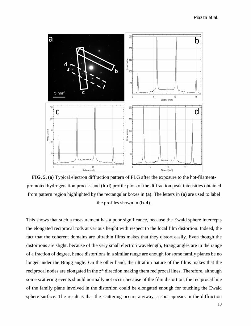
hydrogenation process (FIG. 5).
FIG. 5a shows typical electron diffraction pattern of a single FLG domain after the exposure
to the hot-filament-promoted hydrogenation process. FIG. 5b-d display the profile plots of the
diffraction peak intensities obtained from pattern regions highlighted by the rectangular boxes in
FIG. 5a. FIG. 5b-d only show three of the six profiles for clarity purpose. For half of the profile
lines, the intensity of the spots of the 1st family planes (closest to the center of the pattern) is higher
than the intensity of the spots of the 2nd family planes (FIG. 5b and 5c). This is similar to what was
reported for F-diamane in [14]. However, for the other half of the intensity profiles, there is no clear
trend and the situation differs from the ideal case (FIG. 5d).
Piazza et al.
13
FIG. 5. (a) Typical electron diffraction pattern of FLG after the exposure to the hot-filament-
promoted hydrogenation process and (b-d) profile plots of the diffraction peak intensities obtained
from pattern region highlighted by the rectangular boxes in (a). The letters in (a) are used to label
the profiles shown in (b-d).
This shows that such a measurement has a poor significance, because the Ewald sphere intercepts
the elongated reciprocal rods at various height with respect to the local film distortion. Indeed, the
fact that the coherent domains are ultrathin films makes that they distort easily. Even though the
distortions are slight, because of the very small electron wavelength, Bragg angles are in the range
of a fraction of degree, hence distortions in a similar range are enough for some family planes be no
longer under the Bragg angle. On the other hand, the ultrathin nature of the films makes that the
reciprocal nodes are elongated in the z* direction making them reciprocal lines. Therefore, although
some scattering events should normally not occur because of the film distortion, the reciprocal line
of the family plane involved in the distortion could be elongated enough for touching the Ewald
sphere surface. The result is that the scattering occurs anyway, a spot appears in the diffraction
Piazza et al.
14
pattern which actually is a cross-section of the reciprocal line by the Ewald sphere, but the intensity
of the spot cannot be the nominal one because the Ewald sphere does not cross the reciprocal line at
its maximum intensity but at various height depending on the distortion. This corresponds to the
“interference error” effect well-known by transmission electron microscopists. Therefore, one could
not expect discriminate between the various possible structures based on the analysis of spot
intensities either.
In some regions of the FLG after exposure to the hot-filament-promoted hydrogenation
process, electron diffraction patterns differ from the typical patterns of pristine FLG and/or of pure
ultrathin and crystalline sp3–C sheets. FIG. 6 displays some examples of such patterns taken from
different flakes. Over 53 flakes analyzed, such patterns were not observed in pristine FLG. The
complex patterns shown in FIG. 6 including satellite peaks are characteristic of patterns for twisted
superimposed coherent domains (TCD) with similar periodicities of very small twisted angle, and
with secondary periodicity [28,29]. Referring to the model in FIG. 1, such TCDs could be the upper
diamanoïd domain (represented by L1 and L2, completed with L3) and the lower graphenic domain
(represented by L4 and other graphenes underneath) – see the introduction to the model in Section
2.4. Therefore, at the interface between the two twisted domains are two graphene layers (L3 and
L4) which are in twisted configuration. Twisted bilayer (TBL) with very small twisted angle is a
system recently studied [28,29] which generates specific Raman signatures [30]. Therefore, FIG. 6
reveals such an occurrence of TCDs upon hydrogenation.

Piazza et al.
15
FIG. 6. (a to f) Typical diffraction patterns of specimen flakes after the exposure to the hot-
filament-promoted hydrogenation process.
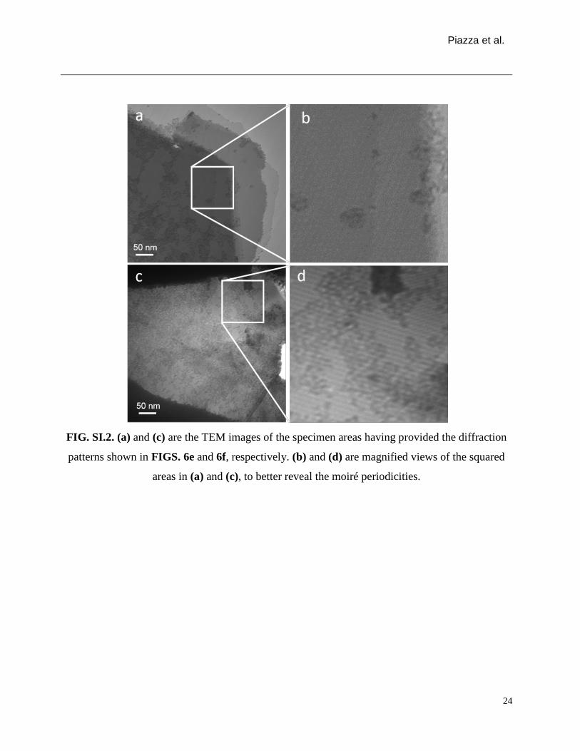
This interpretation is supported by the observation of moiré patterns in TEM images typical of such
twisted systems (FIG. SI.2.) and the detection of the specific peaks observed at ~1385 cm-1 and in

Piazza et al.
16
~1669 cm-1 in UV Raman spectra (TBL1 and TBL2 in FIG. 7), which were previously reported for
TBL [30].
It is supposed that the slight rotation of the superimposed domains from the TCDs is induced
by the relaxation of huge (several GPa) local constraints which develop between superimposed
layers as a result of the sp2–C-to-sp3–C conversion. In diamond-like carbon, a material that contains
a variable fraction of sp3–C and sp2–C, internal stress can reach several GPa [9,10,31]. This will be
further discussed below.
FIG. 7. Typical UV Raman spectrum of a specimen flake after the exposure to the hot-filament-
promoted hydrogenation process showing peaks typical of twisted bilayer graphene, labeled TBL1
and TBL2. Those peaks are also present in the Raman spectrum in FIG. 2. The G band reveals the
partial conversion only.
Together with the sharp stretching mode at 1319-1337 cm-1 and assigned to lonsdaleite or diamond,
UV Raman spectra of hydrogenated samples display a sharp T peak at 1055-1071 cm-1 assigned to
bonding between sp3–C (FIG. 2 and 7) [2]. We further investigated the physical origin of this T
peak by using DFT calculations. For pure sp2–C and sp3–C materials, no T peak is present. We have
already reported [2] a spatial correlation between the occurrence of the diamond/lonsdaleite
stretching mode peak and that of the T peak while there is no spatial correlation between the location

Piazza et al.
17
of the G peak and that of the T peak. Thus, we have hypothesised that the T peak could be related
to the interface between a sp2–C layer and a sp3–C layer, and consequently we have investigated the
phonon dispersion of the ABBA-stacking model proposed in FIG. 1. Upon full atomic relaxation,
all frequencies remain positive, proving the stability of the proposed structure. Three distinct Raman
active modes in the range of interest are present, with wavenumbers from 1050 to 1100 cm-1 (FIG.
8). Normal mode analysis shows that two of them, which correspond to a large rotation of hydrogen
atoms (see SI.3 for atomic vector representation), are degenerated with a wavenumber of 1099 cm-
1 at the center of the Brillouin zone (Γ point) and are visible in Raman spectra. Interestingly, the
mode at 1078 cm-1, which involves atoms from L1 and L2, can be associated to a combination of
the stretching of the sp3-C bonds with an optical out-of-plane (ZO) mode of graphene membrane.
Due to the periodic repetition of the motif in DFT calculations, delamination is not possible and the
full cell relaxation leads to compressive strain in the sp3–C part (L1-L2) and to extensive strain in
graphene layers (L3-L4, and further layers underneath), explaining the position of the G band which
is downshifted by almost 150 cm-1 in the calculation compared to the pristine graphene (see
FIG. SI.1). Using the conversion factor of 4.5 cm-1/GPa [30], the stress brought to the graphene
domain (L4 and further layers underneath) can be estimated at -33 GPa. Obviously, this is a huge
stress value which is by far enough to generate the delamination and twisting events which occur
experimentally in the material, although the periodic conditions in the calculation cannot account
for them. The system exhibits a perfect, periodic interface contrary to amorphous materials. As a
consequence, the experimental linewidth of the T band is as low as 14.0 cm-1.
In summary, the model presented is FIG.1 together with our DFT calculations are consistent
with characterization results obtained here and in Reference [2]. In particular, the model is able to
account for the five peaks observed in Raman spectra in the 1000-1800 cm-1 wavenumber range.
Besides, the results show that it is not possible to form pure diamanoïds starting from FLG with
ABA… stacking as soon as the number of layers is higher than two. In that case, only the first two
layers will be sp3–C. Also, only the first surface layer will be sp3–C if the starting FLG is turbostratic.
In that case, for some rotation angles, AA and AB configurations may locally occur, allowing local
only sp2–C to sp3–C conversion, that could generate the destruction of the structure or a huge
topological deformation along with huge inner constraints. The formation of diamanoïds with a
number of layers higher than two requires starting from FLG with AAA… or ABC… stacking,
which both are energetically unfavourable, and therefore barely preparable.

Piazza et al.
18
FIG. 8. (a) Phonon dispersion curve of the partially hydrogenated ABBA stacked FLG model
proposed in FIG. 1 based on DFPT calculations. (b) Corresponding vectors associated to the
atomic displacements along the normal mode at 1078 cm-1. Vector lengths are not at the scale of
the model, but are proportional to each other.
4. Conclusion
We reported on new additional evidences, from electron diffraction at 5 keV and Raman
spectroscopy, supported by calculations, confirming the successful conversion of few-layer
graphene into nanometer-thick and crystalline sp3–C sheets from the exposure of FLG to H radicals
produced in a hot-filament process at low temperature and pressure. The results confirmed previous
multi-wavelength Raman spectroscopy and FTIR microscopy analysis. Complex electron diffraction
patterns differing from pristine FLG and including satellite peaks reveal that twisted coherent
domains involving a minimum of one diamanoïd domain and one unconverted graphenic domain
underneath, are formed, presumably due to the relaxation of stress resulting from the partial sp2–C
to sp3–C conversion. A configuration of twisted bilayer graphene (TBL) is created at the interface
between the twisted, superimposed domains. Peaks ascribed to TBL are also evidenced in Raman

Piazza et al.
19
spectra at 1385 cm-1 and 1669 cm-1, consistently with the recent literature. Also, by using DFT
calculations, the exact origin of the T peak was revealed. It originates from a combination of the
sp3–C stretching mode of a C–sp3 layer with the optical out-of-plane mode of a graphene layer; both
layers being sandwiched between a highly hydrogenated sp3–C surface layer and the underneath
unconverted graphene layer (s), and interacting strongly because of the presence of free pz orbitals
in the sp3–C layer. The frequent evidence of sp3–C to sp2–C partial conversion confirms that starting
from FLG with both a number of layers higher than two and the Bernal (ABA…) stacking sequences,
which is the most frequent configuration by far, is not favourable for producing diamanoïds.
However, this may be used for the fabrication of graphene/diamanoïd heterostructures. The
formation of diamanoïds with a number of layer higher than two requires specific stacking sequences
other than Bernal which are energetically unfavourable, and therefore difficult to synthesize. It is
expected to elaborate large area diamane layer by using Bernal-stacked bi-layer graphene as pristine
material.
Acknowledgements
This research was funded by the Ministry of Higher Education, Science and Technology
(MESCyT) of the Dominican Republic (2010-2011, 2012, 2015 and 2016-2018 FONDOCyT
programs). F.P. and M.M. greatly acknowledge MESCyT and PUCMM for strong financial,
administrative and technical support; 2017 NEXT Guest scientist Program and the French Embassy
in the Dominican Republic for travel support. I.C.G. acknowledges the Calcul en Midi-Pyrénées
initiative CALMIP (Project p0812) for allocations of computer time, as well as GENCI-CINES and
GENCI-IDRIS for Grant No. 2019-A006096649.
References
[1] Chernozatonskii L.A.; Sorokin P.B.; Kvashnin A.; Kvashnin D.G. Diamond-Like C2H
Nanolayer, Diamane: Simulation of the Structure and Properties., J Exp Theor Phys Lett (2009) 90,
134-138.
Piazza et al.
20
[2] Piazza F.; Gough K.; Monthioux M.; Puech P.; Gerber I.; Wiens R.; Paredes G.; Ozoria C. Low
Temperature, Pressureless sp2 to sp3 Transformation of Ultrathin, Crystalline Carbon Films., Carbon
(2019) 145, 10-22.
[3] Chernozatonskii L.A.; Sorokin P.B.; Kuzubov A.A.; Sorokin B.P.; Kvashnin A.G.; Kvashnin
D.G.; et al. Influence of Size Effect on the Electronic and Elastic Properties of Diamond Films with
Nanometer Thickness., J Phys Chem C (2011) 115,132-136.
[4] Chernozatonskii L.A.; Mavrin B.N.; Sorokin P.B. Determination of ultrathin diamond films by
Raman spectroscopy., Phys Status Solidi B (2012) 249, 1550-1554.
[5] Ruoff R.S. Personal perspectives on graphene: New graphene-related materials on the horizon.,
Mat Res Soc Bulletin (2012) 37, 1314-1318.
[6] Gupta S.; Yang J.H.; Yakobson B.I. Two-Level Quantum Systems in Two-Dimensional
Materials for Single Photon Emission., Nano Lett (2019) 19(1) 408-414.
[7] Fiori G.; Bonaccorso F.; Iannaccone G.; Palacios T. ; Neumaier D. ; Seabaugh A.; Banerjee S.K.;
Colombo L.; Electronics based on two-dimensional materials., Nature Nanotechnology (2014) 9(10)
768-779.
[8] Rajasekaran S.; Abild-Pedersen F.; Ogasawara H.; Nilsson A.; Kaya S. Interlayer carbon bond
formation induced by hydrogen adsorption in few-layer supported graphene., Phys Rev Lett (2013)
111, 085503-1-058503-5.
[9] Robertson J. Diamond-like amorphous carbon., Mater Sci Eng R (2002) 37, 129-281.
[10] Piazza F. Hard-hydrogenated tetrahedral amorphous carbon films by distributed electron
cyclotron resonance plasma., Int J Refract Met Hard Mater (2006) 24, 39-48.
[11] Barboza A.P.M.; Guimaraes M.H.D.; Massote D.V.P.; Campos L.C.; Barbosa Neto N.M.;
Cancado L.G.; et al. Room temperature compression-induced diamondization of few-layer
graphene., Adv Mater (2011) 23, 3014-3017.
[12] Martins L.G.P.; Matos M.J.S.; Paschoal A.R.; Freire P.T.C.; Andrade N.F.; Aguiar A.L.; Kong
J.; Neves B.R.A.; de Oliveira A.B.; Mazzoni M.S.C.; Filho A.G.S.; Cancado L.G. Raman evidence
for pressure-induced formation of diamondene., Nat Comm (2017) 8 (1) 96 (9 pages).
[13] Gao Y.; Cao T.; Cellini F.; Berger C.; de Heer W.A.; Tosatii E.; Riedo E.; Bongiorno A.
Ultrahard carbon film from epitaxial two-layer graphene., Nature Nanotechnology (2018) 13, 133-
138.
[14] Bakharev P.V.; Huang M.; Saxena M.; Lee S.W.; Joo S.H; Park S.O.; Dong J.; Camacho-
Mojica D.; Jin S.; Kwon Y.; Biswal M.; Ding F.; Kwak S.K.; Lee Z.; Ruoff R.S. Chemically Induced

Piazza et al.
21
Transformation of CVD-Grown Bilayer Graphene into Single Layer Diamond. (2019)
Arxiv.org/abs/1901.02131v1.
[15] J.-T. Wang, C. Chen, E. Wang, Y. Kawazoe, A New Carbon Allotrope with Six-Fold Helical
Chains in all-sp2 Bonding Networks, Scientific Reports 4:4339 (2014) 1-5.
[16] H.A. Calderon, A. Okonkwo, I. Estrada-Guel, V.G. Hadjiev, F. Alvarez-Ramírez, HRTEM low
dose: the unfold of the morphed graphene, from amorphous carbon to morphed graphenes, Adv
Struc Chem Imaging 2 (2016) 10-12.
[17] Regan W, Alem N, Aleman B, Geng B, Girit C, Masareti L et al. A direct transfer of layer-area
graphene. Appl Phys Lett 2010;96:113102-1-113102-3.
[18] Piazza F, Morell G, Beltran-Huarac J, Paredes G, Ahmadi M, Guinel M. Carbon nanotubes
coated with diamond nanocrystals and silicon carbide by hot-filament chemical vapor deposition
below 200 °C substrate temperature. Carbon 2014;75, 113-123.
[19] Neverov, V. S. (2017). XaNSoNS: GPU-accelerated simulator of diffraction patterns of
nanoparticles. SoftwareX, 6, 63-68.
[20] Kresse G, Hafner J. Ab initio molecular dynamics for liquid metals. Phys Rev B 1993;47:558-
561.
[21] Kresse G, Furthmüller J. Efficient iterative schemes for ab initio total-energy calculations using
a plane-wave basis set. Phys Rev B 1996; 54: 11169-11186.
[22] Blöchl PE. Projector augmented-wave method. Phys Rev B 1994;50:17953-17979.
[23] Kresse G, Joubert D. From ultrasoft pseudopotentials to the projector augmented-wave method.
Phys Rev B 1999; 59: 1758-1775.
[24] Perdew JP, Burke K, Ernzerhof M. Generalized Gradient Approximation Made Simple. Phys
Rev Lett 1996;77:3865-3668.
[25] Grimme S, Antony J, Ehrlich S, Krieg H. A consistent and accurate ab initio parametrization
of density functional dispersion correction (DFT-D) for the 94 elements H-Pu. J Chem Phys
2010;132:154104-1-154104-1-19.
[26] Togo A, Tanaka I, First principles phonon calculations in materials science, Scripta Material
2015;108: 1–5.
[27] 2018 International Centre for Diffraction Data.
[28] Zhang K, Tadmor Ellad B. Structural and electron diffraction scaling of twisted graphene
bilayers, J Mechanics Phys Solids 2018; 112: 225-238.

Piazza et al.
22
[29] Yoo H, Engelke R, Carr S, Fang S, Zhang K, Cazeaux P et al. Atomic and electronic
reconstruction at the van der Waals interface in twisted bilayer graphene, Nature Materials 2019;
https://doi.org/10.1038/s41563-019-0346-z.
[30] Eliel GSN, Moutinho MVO, Gadelha AC, Righi A, Campos LC, Ribeiro HB. Intralayer and
interlayer electron-phonon interactions in twisted graphene heterostructures, Nature
Communications 2018, 9:1221; DOI:10.1038/s41467-018-03479-3.
[31] Weiler M, Sattel S, Giessen T, Jung K, Ehrhardt, Veerasamy VS, Robertson J. Preparation and
properties of highly tetrahedral hydrogenated amorphous carbon, Phys Rev B (1996); 53: 1594-
1608.
[30] Hanfland M., Beister H., Syassen K. Graphite under pressure: Equation of state and first-order
Raman modes, Phys. Rev. B (1989); 39 (17), 12598-12603.

Piazza et al.
23
Supplemental Information
FIG. SI.1. Phonon dispersion curve of a pure graphene monolayer.
Piazza et al.
24
FIG. SI.2. (a) and (c) are the TEM images of the specimen areas having provided the diffraction
patterns shown in FIGS. 6e and 6f, respectively. (b) and (d) are magnified views of the squared
areas in (a) and (c), to better reveal the moiré periodicities.

Piazza et al.
25
FIG. SI.3. Vectors associated to the atomic displacements along the two degenerated normal modes
at 1099 cm-1. Only one is depicted here, since the other is simply anti-symmetric in the x-y exchange.
This figure is complementary to FIG. 8. The two modes at 1099 cm-1 correspond to a large rotation
of hydrogen atoms. Since carbon atoms from L2 are not involved, these modes can not account for
the experimental spatial correlation between the T peak and the sp3-C stretching peak [1], contrary
to the mode reported in FIG. 8. All modes are Raman active.
References
[1] Piazza F.; Gough K.; Monthioux M.; Puech P.; Gerber I.; Wiens R.; Paredes G.; Ozoria C. Low
Temperature, Pressureless sp2 to sp3 Transformation of Ultrathin, Crystalline Carbon Films., Carbon
(2019) 145, 10-22.