totem technologies for analog, memory, mixed-signal designs
TRANSCRIPT

© 2014 ANSYS, Inc.6/23/2014 111
Totem™ Technologies for Analog / Memory / Mixed-Signal Designs
Design Automation Conference 2014

© 2014 ANSYS, Inc.6/23/2014 222
Analog Mixed-Signal Trends & Challenges
Technology Scaling
High Analog + Digital Integration
Increasing Sensor/IP usage
Capacity
Tighter Reliability Margins
Concurrent
Analog +Digital Analysis
Sensor/IP
Validation and Modeling
>$60B
Mobile Computing
Automotive Electronics
IoT/Connected Devices
Key Market Drivers Technology Trends Challenges
Analog IC market expected to grow to $60B by 2015
Transition from discrete analog to analog subsystems
Complex verification and integration challenges
© 2014 ANSYS, Inc.6/23/2014 333
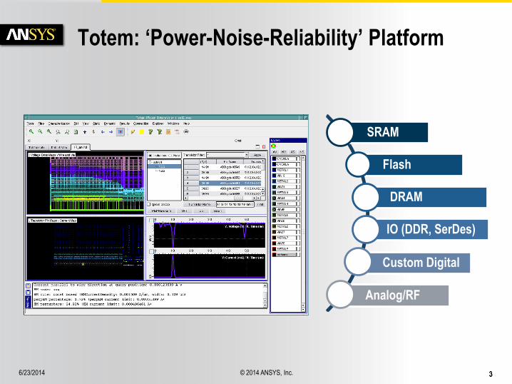
Totem: ‘Power-Noise-Reliability’ Platform
SRAM
Flash
DRAM
IO (DDR, SerDes)
Custom Digital
Analog/RF

© 2014 ANSYS, Inc.6/23/2014 444
Totem: Core Technologies
Analysis
Modeling
• Support for complex analog and mixed signal designs
• Transient analysis with ps resolution
• EM/ESD analysis for advanced technology nodes
• Transistor-level macro models
• Multi-cycle Multi-mode models
• Model roll up to SoC
CMM
Totem RedHawk
Extraction
• On-chip PG RLC + Substrate RC extraction
• EM aware extraction
© 2014 ANSYS, Inc.6/23/2014 555
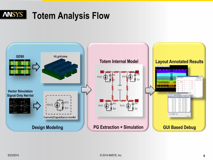
PG Extraction + SimulationDesign Modeling
Totem Analysis Flow
GDSII
Vector Simulation
Signal Only Net-list
Totem Internal Model
GUI Based Debug
Layout Annotated Results
© 2014 ANSYS, Inc.6/23/2014 666
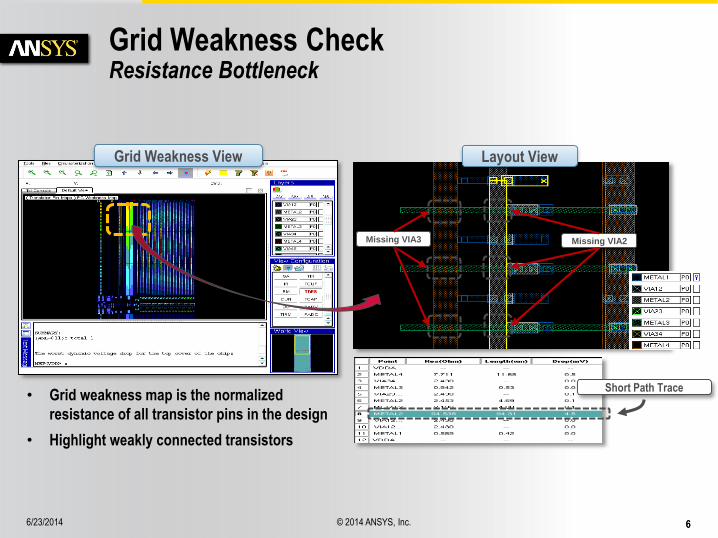
Grid Weakness Check Resistance Bottleneck
Layout ViewGrid Weakness View
Missing VIA2Missing VIA3
Short Path Trace• Grid weakness map is the normalized
resistance of all transistor pins in the design
• Highlight weakly connected transistors

© 2014 ANSYS, Inc.6/23/2014 777
Case Study: Analog IP
Analog Supply IR Map
Metal3 strap not
extended
Gross Connectivity IssueLayout View
Early layout analysis helps
catch gross grid violations
© 2014 ANSYS, Inc.6/23/2014 888
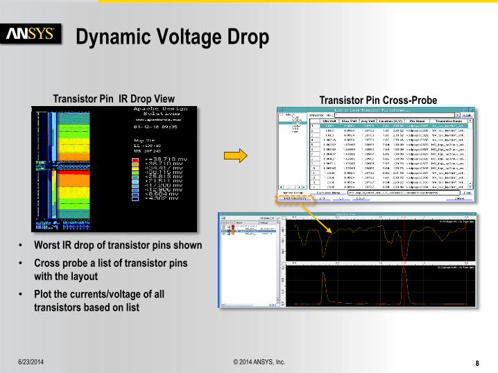
Dynamic Voltage Drop
• Worst IR drop of transistor pins shown
• Cross probe a list of transistor pins
with the layout
• Plot the currents/voltage of all
transistors based on list
Transistor Pin Cross-ProbeTransistor Pin IR Drop View
© 2014 ANSYS, Inc.6/23/2014 999
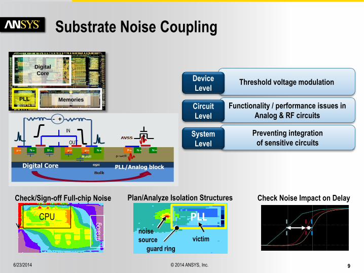
Substrate Noise Coupling
Digital
Core
MemoriesPLL
IN
OUT
PLL/Analog blockDigital Core
Threshold voltage modulationDevice
Level
Functionality / performance issues in
Analog & RF circuitsCircuit
Level
Preventing integration
of sensitive circuitsSystem
Level
anal
og
CPU
Check/Sign-off Full-chip Noise
PLL
guard ring
noise
source victim
Plan/Analyze Isolation Structures Check Noise Impact on Delay

© 2014 ANSYS, Inc.6/23/2014 101010
Chip Image Sensors: Key Challenges
Substrate

© 2014 ANSYS, Inc.6/23/2014 111111
Chip Image Sensors: Key Challenges
Substrate
Digital Logic
(Interface, Timing, Processing Output)
ADC
Analog to Digital Conversion
Pixel ArrayAnalog
Signal
Processing
Substrate
Noise Coupling
• Digital Switching Noise
• PG Grid Coupling
• Substrate Noise Coupling

© 2014 ANSYS, Inc.6/23/2014 121212
Chip Image Sensors: Key Challenges
Power Noise Analysis
• Digital Logic (Vectored/Vectorless)
• Analog (Vectored)
• Substrate Noise (Digital +Analog)
Substrate
Digital Logic
(Interface, Timing, Processing Output)
ADC
Analog to Digital Conversion
Pixel ArrayAnalog
Signal
Processing
Substrate
Noise Coupling
• Digital Switching Noise
• PG Grid Coupling
• Substrate Noise Coupling
© 2014 ANSYS, Inc.6/23/2014 131313
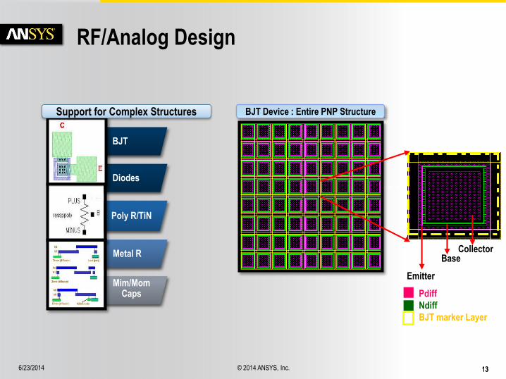
BJT
Poly R/TiN
Metal R
Mim/Mom Caps
Diodes
RF/Analog Design
Support for Complex Structures BJT Device : Entire PNP Structure
Emitter
BaseCollector
Pdiff
Ndiff
BJT marker Layer
© 2014 ANSYS, Inc.6/23/2014 141414
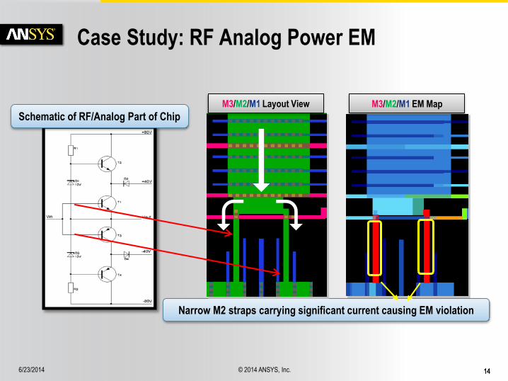
Case Study: RF Analog Power EM
Schematic of RF/Analog Part of Chip
Narrow M2 straps carrying significant current causing EM violation
M3/M2/M1 EM MapM3/M2/M1 Layout View
© 2014 ANSYS, Inc.6/23/2014 151515
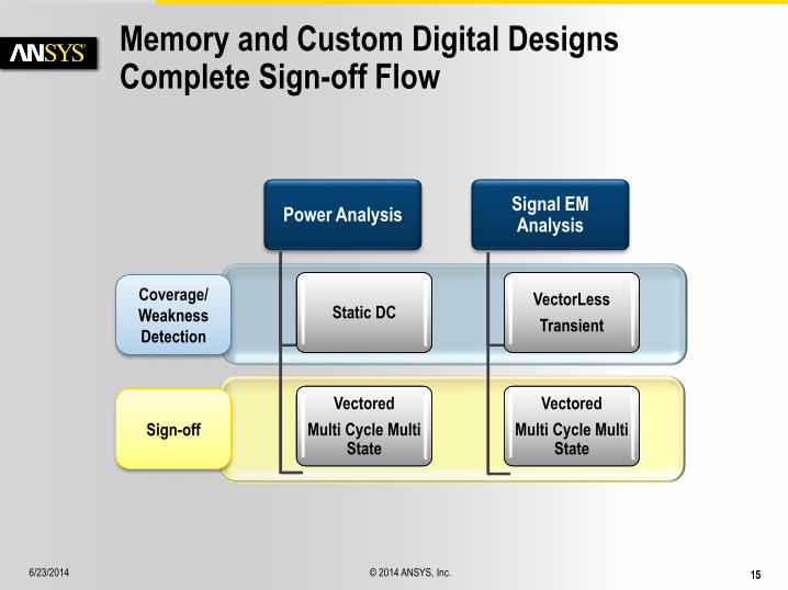
Memory and Custom Digital DesignsComplete Sign-off Flow
Coverage/
Weakness
Detection
Sign-off
Power Analysis
Static DC
Vectored
Multi Cycle Multi State
Signal EM Analysis
VectorLess
Transient
Vectored
Multi Cycle Multi State

© 2014 ANSYS, Inc.6/23/2014 161616
Large FPGA Chip
Small Design Large Design
Node Count 14M 321M
Transistor
Count
7M 228M
Run Time 39mins 20h22m
• Full-chip capacity
• Large DRAM memories
• Large FLASH memories
• Embedded Big Analog,
Small Digital blocks
FPGA Faric with
rows of
SRAM, DSP blocks
System
Controller
DDR
Memory and
Other
IP Blocks
IOIO
Large Design Handling
© 2014 ANSYS, Inc.6/23/2014 171717
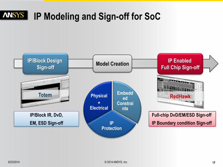
IP Modeling and Sign-off for SoC
IP/Block Design
Sign-off
IP/Block IR, DvD,
EM, ESD Sign-off
Totem
IP Enabled
Full Chip Sign-off
Full-chip DvD/EM/ESD Sign-off
IP Boundary condition Sign-off
RedHawk
Model Creation
Embedded
Constraints
IP Protection
Physical
+ Electrical
© 2014 ANSYS, Inc.6/23/2014 181818
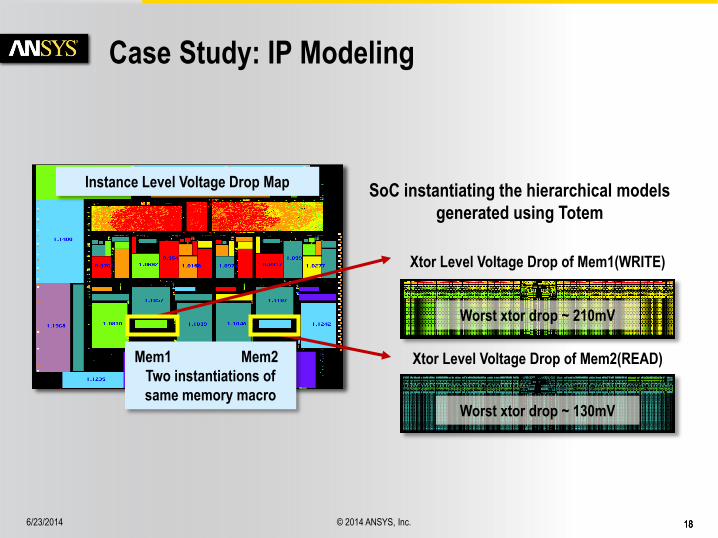
Case Study: IP Modeling
Xtor Level Voltage Drop of Mem1(WRITE)
Xtor Level Voltage Drop of Mem2(READ)
Worst xtor drop ~ 210mV
Worst xtor drop ~ 130mV
Mem1 Mem2
Two instantiations of
same memory macro
Instance Level Voltage Drop MapSoC instantiating the hierarchical models
generated using Totem
© 2014 ANSYS, Inc.6/23/2014 191919
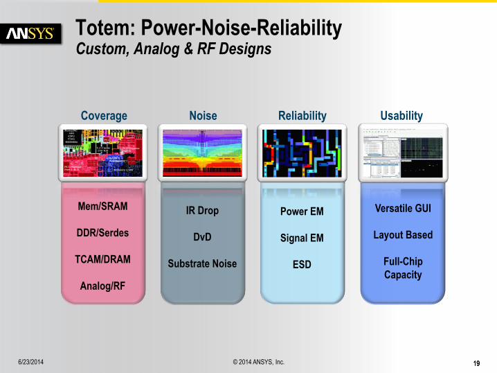
Totem: Power-Noise-ReliabilityCustom, Analog & RF Designs
Noise
CouplingReliabilityCoverage Usability
IR Drop
DvD
Substrate Noise
Power EM
Signal EM
ESD
Mem/SRAM
DDR/Serdes
TCAM/DRAM
Analog/RF
Versatile GUI
Layout Based
Full-Chip
Capacity
Coverage Noise Reliability Usability