top menu menu standby/on open/close menuhome enter return rrv3584 dvd player...
TRANSCRIPT
PIONEER CORPORATION 4-1, Meguro 1-chome,PIONEER ELECTRONICS (USA) INC. P.O. Box 1760, LonPIONEER EUROPE NV Haven 1087, Keetberglaan 1, 912PIONEER ELECTRONICS ASIACENTRE PTE. LTD. 253
PIONEER CORPORATION 2007
TOP MENU MENU
RETURN
ENTERHOMEMENUOPEN/CLOSE
STANDBY/ON
DV-300-K
Meguro-ku, Tokyo 153-8654, Japang Beach, CA 90801-1760, U.S.A.
0 Melsele, BelgiumAlexandra Road, #04-01, Singapore 159936
ORDER NO.
RRV3584
DVD PLAYER
DV-300-KTHIS MANUAL IS APPLICABLE TO THE FOLLOWING MODEL(S) AND TYPE(S).
Model Type Power Requirement Region No. Remarks
DV-300-K KUCXZT AC 120 V 1
For details, refer to "Important Check Points for Good Servicing" .
T-ZZV APR. 2007 printed in Japan

C
D
F
A
B
E
1 2 3 4SAFETY INFORMATION
This service manual is intended for qualified service technicians; it is not meant for the casualdo-it-yourselfer. Qualified technicians have the necessary test equipment and tools, and have beentrained to properly and safely repair complex products such as those covered by this manual.Improperly performed repairs can adversely affect the safety and reliability of the product and mayvoid the warranty. If you are not qualified to perform the repair of this product properly and safely, youshould not risk trying to do so and refer the repair to a qualified service technician.
WARNING
This product contains lead in solder and certain electrical parts contain chemicals which are known to the state of California to
cause cancer, bir th defects or other reproductive harm.
Health & Safety Code Section 25249.6 – Proposition 65
NOTICE
(FOR CANADIAN MODEL ONLY)
Fuse symbols (fast operating fuse) and/or (slow operating fuse) on PCB indicate that replacement
parts must be of identical designation.
REMARQUE
(POUR MODÈLE CANADIEN SEULEMENT)
Les symboles de fusible (fusible de type rapide) et/ou (fusible de type lent) sur CCI indiquent que
les pièces de remplacement doivent avoir la même désignation.
ANY MEASUREMENTS NOT WITHIN THELIMITS OUTLINED ABOVE ARE INDICATIVEOF A POTENTIAL SHOCK HAZARD ANDMUST BE CORRECTED BEFORE RETURN-ING THE APPLIANCE TO THE CUSTOMER.
2. PRODUCT SAFETY NOTICEMany electrical and mechanical parts in the appliance
have special safety related character istics. These areoften not evident f rom visual inspect ion nor theprotection afforded by them necessarily can be obtainedby using replacement components rated for voltage,wattage, etc. Replacement par ts which have thesespecial safety character ist ics are identif ied in thisService Manual.
Electr ical components having such features areidentified by marking with a on the schematics andon the parts list in this Service Manual.The use of a substitute replacement component whichdoes not have the same safety characteristics as thePIONEER recommended replacement one, shown in theparts list in this Service Manual, may create shock, fire,or other hazards.
Product Safety is continuously under review and newinstructions are issued from time to time. For the latestinformation, always consult the current PIONEERService Manual. A subscription to, or additional copiesof, PIONEER Service Manual may be obtained at anominal charge from PIONEER.
(FOR USA MODEL ONLY)1. SAFETY PRECAUTIONS
The following check should be performed for thecont inued protect ion of the customer and servicetechnician.
LEAKAGE CURRENT CHECKMeasure leakage current to a known ear th ground
(water pipe, conduit, etc.) by connecting a leakagecurrent tes ter such as S impson Model 229-2 orequivalent between the earth ground and all exposedmetal par ts of the appliance (input/output terminals,screwheads, metal overlays, control shaft, etc.). Plugthe AC line cord of the appliance directly into a 120VAC 60 Hz outlet and turn the AC power switch on. Anycurrent measured must not exceed 0.5 mA.
Deviceundertest
Leakagecurrenttester
Earthground
Reading shouldnot be above0.5 mA
Also test withplug reversed(Using AC adapterplug as required)
Test allexposed metalsurfaces
AC Leakage Test
DV-300-K21 2 3 4
C
D
F
A
B
E
3
5 6 7 8
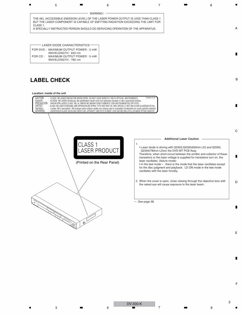
WARNING !
THE AEL (ACCESSIBLE EMISSION LEVEL) OF THE LASER POWER OUTPUT IS LESS THAN CLASS 1 BUT THE LASER COMPONENT IS CAPABLE OF EMITTING RADIATION EXCEEDING THE LIMIT FOR CLASS 1.A SPECIALLY INSTRUCTED PERSON SHOULD DO SERVICING OPERATION OF THE APPARATUS.
LASER DIODE CHARACTERISTICS
FOR DVD : MAXIMUM OUTPUT POWER : 5 mWWAVELENGTH : 650 nm
FOR CD : MAXIMUM OUTPUT POWER : 5 mWWAVELENGTH : 780 nm
Additional Laser Caution
∗ : See page 28.
1.• Laser diode is driving with Q2303,Q2305(650nm LD) and Q2302, Q2304(780nm LD)on the DVD MT PCB Assy.Therefore, when short-circuit between the emitter and collector of these transistors or the base voltage is supplied for transistors turn on, the laser oscillates. (failure mode)• In the test mode ∗ , there is the mode that the laser oscillates except for the disc judgment and playback. LD ON mode in the test mode oscillates with the laser forcibly.
2. When the cover is open, close viewing through the objective lens with the naked eye will cause exposure to the laser beam.
LABEL CHECK
(Printed on the Rear Panel)
Location: inside of the unit
TOP MENU
MENU
RETURN
ENTER
HOMEMENU
OPEN/CLOSE
STANDBY/ON
DV-300-K5 6 7 8

C
D
F
A
B
E
DV-300-K4
1 2 3 4
[Important Check Points for Good Servicing]In this manual, procedures that must be performed during repairs are marked with the below symbol.Please be sure to confirm and follow these procedures.
1. Product safety
Please conform to product regulations (such as safety and radiation regulations), and maintain a safe servicing environment by following the safety instructions described in this manual.
1 Use specified parts for repair.
Use genuine parts. Be sure to use important parts for safety.
2 Do not perform modifications without proper instructions.
Please follow the specified safety methods when modification(addition/change of parts) is required due to interferences such as radio/TV interference and foreign noise.
3 Make sure the soldering of repaired locations is properly performed.
When you solder while repairing, please be sure that there are no cold solder and other debris.Soldering should be finished with the proper quantity. (Refer to the example)
4 Make sure the screws are tightly fastened.
Please be sure that all screws are fastened, and that there are no loose screws.
5 Make sure each connectors are correctly inserted.
Please be sure that all connectors are inserted, and that there are no imperfect insertion.
6 Make sure the wiring cables are set to their original state.
Please replace the wiring and cables to the original state after repairs.In addition, be sure that there are no pinched wires, etc.
7 Make sure screws and soldering scraps do not remain inside the product.
Please check that neither solder debris nor screws remain inside the product.
8 There should be no semi-broken wires, scratches, melting, etc. on the coating of the power cord.
Damaged power cords may lead to fire accidents, so please be sure that there are no damages.If you find a damaged power cord, please exchange it with a suitable one.
9 There should be no spark traces or similar marks on the power plug.
When spark traces or similar marks are found on the power supply plug, please check the connection and advise on secure connections and suitable usage. Please exchange the power cord if necessary.
0 Safe environment should be secured during servicing.
When you perform repairs, please pay attention to static electricity, furniture, household articles, etc. in order to prevent injuries. Please pay attention to your surroundings and repair safely.
2. Adjustments
To keep the original performance of the products, optimum adjustments and confirmation of characteristics within specification.Adjustments should be performed in accordance with the procedures/instructions described in this manual.
4. Cleaning
For parts that require cleaning, such as optical pickups, tape deck heads, lenses and mirrors used in projection monitors, proper cleaning should be performed to restore their performances.
3. Lubricants, Glues, and Replacement parts
Use grease and adhesives that are equal to the specified substance. Make sure the proper amount is applied.
5. Shipping mode and Shipping screws
To protect products from damages or failures during transit, the shipping mode should be set or the shipping screws should be installed before shipment. Please be sure to follow this method especially if it is specified in this manual.
1 2 3 4

C
D
F
A
B
E
5
5 6 7 8
CONTENTS SAFETY INFORMATION......................................................................................................................................21. SERVICE PRECAUTIONS ................................................................................................................................6
1.1 NOTES ON SOLDERING...........................................................................................................................61.2 WHEN REPLACING DVD DECK................................................................................................................61.3 DISC REMOVAL METHOD ........................................................................................................................7
2. SPECIFICATIONS.............................................................................................................................................82.1 ACCESSORIES..........................................................................................................................................82.2 SPECIFICATIONS ......................................................................................................................................92.3 DISC/CONTENT FORMAT.......................................................................................................................102.4 PANEL FACILITIES...................................................................................................................................12
3. BASIC ITEMS FOR SERVICE ........................................................................................................................153.1 CHECK POINTS AFTER SERVICING .....................................................................................................153.2 PCB LOCATIONS.....................................................................................................................................163.3 JIGS LIST .................................................................................................................................................17
4. BLOCK DIAGRAM ..........................................................................................................................................184.1 OVERALL WIRING CONNECTION DIAGRAM ........................................................................................184.2 OVERALL BLOCK DIAGRAM ..................................................................................................................204.3 DVD LOADER BLOCK DIAGRAM............................................................................................................214.4 POWER BLOCK DIAGRAM .....................................................................................................................22
5. DIAGNOSIS ....................................................................................................................................................235.1 TROUBLE SHOOTING.............................................................................................................................235.2 METHOD FOR DIAGNOSING DEGRADATION OF THE LDS ON THE PICKUP ASSY .........................27
6. SERVICE MODE .............................................................................................................................................286.1 SERVICE MODE PROCEDURE ..............................................................................................................286.2 SERVICE MODE IN..................................................................................................................................296.3 DISPLAY SPECIFICATION OF THE SERVICE MODE ............................................................................306.4 FUNCTIONAL SPECIFICATION OF THE SHORTCUT KEY ...................................................................316.5 FUNCTIONAL SPECIFICATION OF THE SERVICE MODE ....................................................................32
7. DISASSEMBLY ...............................................................................................................................................337.1 EXTERIOR SECTION ..............................................................................................................................337.2 DVD DECK SECTION ..............................................................................................................................34
8. EACH SETTING AND ADJUSTMENT ............................................................................................................388.1 ADJUSTMENT..........................................................................................................................................388.2 RE-WRITE FOR DVD FIRMWARE...........................................................................................................38
9. EXPLODED VIEWS AND PARTS LIST...........................................................................................................409.1 PACKING SECTION .................................................................................................................................409.2 EXTERIOR SECTION ..............................................................................................................................429.3 06 DVD MECHA SECTION ......................................................................................................................44
10. SCHEMATIC DIAGRAM ................................................................................................................................4610.1 DVD MT PCB ASSY (1/6).......................................................................................................................4610.2 DVD MT PCB ASSY(2/6)........................................................................................................................4810.3 DVD MT PCB ASSY(3/6)........................................................................................................................5010.4 DVD MT PCB ASSY(4/6)........................................................................................................................5210.5 DVD MT PCB ASSY(5/6)........................................................................................................................5410.6 DVD MT PCB ASSY(6/6)........................................................................................................................5610.7 OPERATION 1 and OPERATION 2 PCB ASSYS...................................................................................5810.8 POWER PCB ASSY ...............................................................................................................................6010.9 WAVE FORMS........................................................................................................................................62
11. PCB CONNECTION DIAGRAM ....................................................................................................................6311.1 LOADING MOTOR/SW...........................................................................................................................6411.2 DVD MT PCB ASSY ...............................................................................................................................6411.3 OPERATION 1 PCB and OPERATION 2 PCB ASSYS ..........................................................................6611.4 POWER PCB ASSY ...............................................................................................................................67
12. PCB PARTS LIST ..........................................................................................................................................69
DV-300-K5 6 7 8

C
D
F
A
B
E
DV-300-K6
1 2 3 4
1. SERVICE PRECAUTIONS1.1 NOTES ON SOLDERING
1.2 WHEN REPLACING DVD DECK
NOTES ON SOLDERING• For environmental protection, lead-free solder is used on the printed circuit boards mounted in this unit.
Be sure to use lead-free solder and a soldering iron that can meet specifications for use with lead-free solders for repairsaccompanied by reworking of soldering.
• Compared with conventional eutectic solders, lead-free solders have higher melting points, by approximately 40 ºC. Therefore, for lead-free soldering, the tip temperature of a soldering iron must be set to around 373 ºC in general, althoughthe temperature depends on the heat capacity of the PC board on which reworking is required and the weight of the tip of the soldering iron.
Do NOT use a soldering iron whose tip temperature cannot be controlled.
Compared with eutectic solders, lead-free solders have higher bond strengths but slower wetting times and higher melting temperatures (hard to melt/easy to harden).
The following lead-free solders are available as service parts:• Parts numbers of lead-free solder:
GYP1006 1.0 in dia.GYP1007 0.6 in dia.GYP1008 0.3 in dia.
Before removing Pick Up PCB and DVD PCB connector, short circuit the position shown in Fig. 1 usinga soldering iron. If you remove the DVD Deck with no soldering, the Laser may be damaged.
WHEN REPLACING DVD DECK
[ Removing the DVD Deck ]
[ Installing the DVD Deck ]
Remove all the soldering on the short circuit position after the connection of Pick Up PCB and DVDPCB connector.
NOTE
Fig. 1
Before your operation, please read “PREPARATION OF SERVICING” .Use the Lead Free solder.Manual soldering conditions• Soldering temperature: 320 ± 20˚C• Soldering time: Within 3 seconds• Soldering combination: Sn-3.0Ag-0.5CuWhen Soldering/Removing of solder, use the draw in equipment over the Pick Up Unit to prevent theFlux smoke from it.
•••
•
Short circuit using asoldering iron.
Pick Up PCB
1 2 3 4

C
D
F
A
B
E
7
5 6 7 8
1.3 DISC REMOVAL METHOD
The laser diode used for a pickup head may be destroyed with external static electricity.Moreover, even if it is operating normally after repair, when static electricity discharge isreceived at the time of repair, the life of the product may be shortened.Please perform the following measure against static electricity, be careful of destruction of alaser diode at the time of repair.
• Place the unit on a workstation equipped to protect against static electricity, such as conductive mat.• Soldering iron with ground wire or ceramic type is used.• A worker needs to use a ground conductive wrist strap for body.
PREPARATION OF SERVICING
If the stored 4 digit password in the Rating Level menu needs to be cancelled, please follow the stepsbelow.
Set the DVD to the Stand-by Mode.Press and hold the 'STOP' key on the front panel.Simultaneously press and hold the POWER key on the front panel.The 4 digit password has now been cleared.
1.2.3.4.
PARENTAL CONTROL - RATING LEVEL4 DIGIT PASSWORD CANCELLATION
NOTE: The above procedure will reset ALL of the player's settings to the default factory state.
Slide the Rack Loading (White) toward the arrow direction by using a minus driver to release the lock.(Refer to Fig. 1)Manually open the Tray.
Please strongly pushing Rack Loading (White) to release the lock because the tray doesn't go outeasily.
1.
2.
Fig. 1
Rack Loading (White)
DVD Player (Bottom Side)
NOTE:
DISC REMOVAL METHOD AT NO POWER SUPPLY
DV-300-K5 6 7 8

C
D
F
A
B
E
DV-300-K8
1 2 3 4
2. SPECIFICATIONS2.1 ACCESSORIES
Accessories
• Remote control ×1(07650KY060)
• Audio / Video cable(1.2m) ×1(red/white/yellow)
(06CPBA2006)
• Dry cell batteries ×2(AA/R6P) • Warranty Card
• Operating Instructions
1 2 3 4
C
D
F
A
B
E
9
5 6 7 8
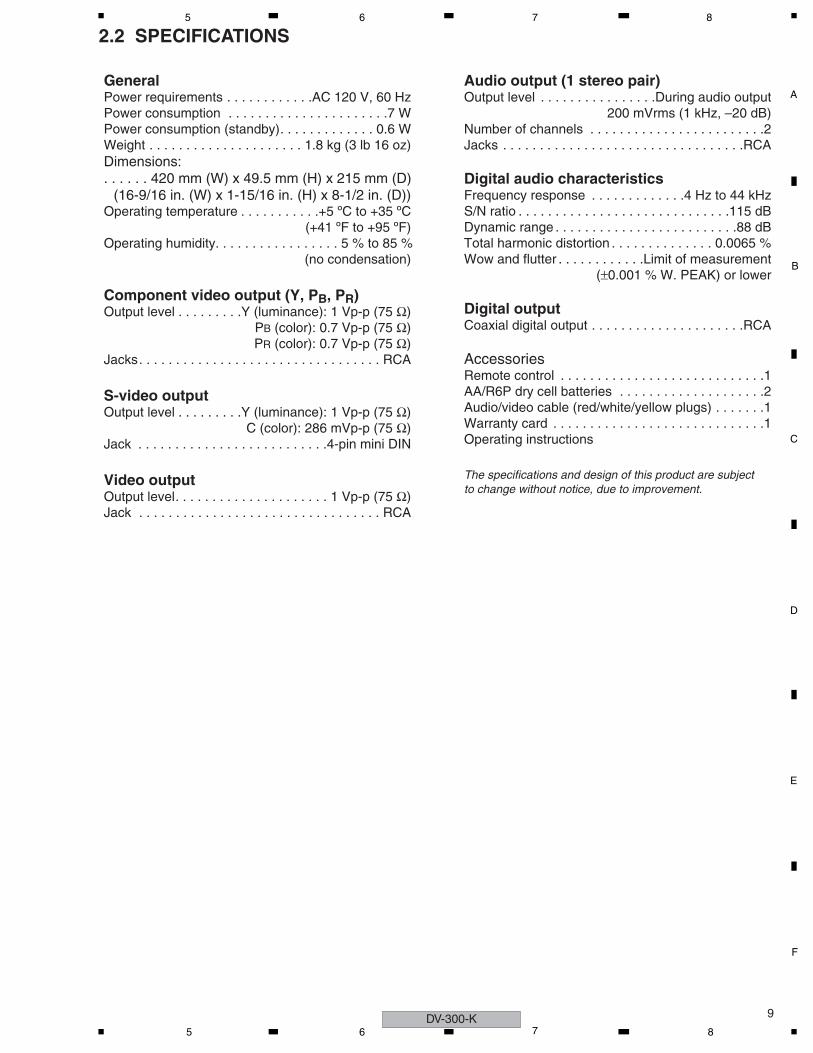
2.2 SPECIFICATIONS
GeneralPower requirements . . . . . . . . . . . .AC 120 V, 60 HzPower consumption . . . . . . . . . . . . . . . . . . . . . .7 WPower consumption (standby). . . . . . . . . . . . . 0.6 WWeight . . . . . . . . . . . . . . . . . . . . . 1.8 kg (3 lb 16 oz)Dimensions:. . . . . . 420 mm (W) x 49.5 mm (H) x 215 mm (D)
(16-9/16 in. (W) x 1-15/16 in. (H) x 8-1/2 in. (D))Operating temperature . . . . . . . . . . .+5 ºC to +35 ºC
(+41 ºF to +95 ºF)Operating humidity. . . . . . . . . . . . . . . . . 5 % to 85 %
(no condensation)
Component video output (Y, PB, PR)Output level . . . . . . . . .Y (luminance): 1 Vp-p (75 Ω)
PB (color): 0.7 Vp-p (75 Ω)PR (color): 0.7 Vp-p (75 Ω)
Jacks. . . . . . . . . . . . . . . . . . . . . . . . . . . . . . . . . RCA
S-video outputOutput level . . . . . . . . .Y (luminance): 1 Vp-p (75 Ω)
C (color): 286 mVp-p (75 Ω)Jack . . . . . . . . . . . . . . . . . . . . . . . . . .4-pin mini DIN
Video outputOutput level. . . . . . . . . . . . . . . . . . . . . 1 Vp-p (75 Ω)Jack . . . . . . . . . . . . . . . . . . . . . . . . . . . . . . . . . RCA
Audio output (1 stereo pair)Output level . . . . . . . . . . . . . . . .During audio output
200 mVrms (1 kHz, –20 dB)Number of channels . . . . . . . . . . . . . . . . . . . . . . . .2Jacks . . . . . . . . . . . . . . . . . . . . . . . . . . . . . . . . .RCA
Digital audio characteristicsFrequency response . . . . . . . . . . . . .4 Hz to 44 kHzS/N ratio . . . . . . . . . . . . . . . . . . . . . . . . . . . . .115 dBDynamic range . . . . . . . . . . . . . . . . . . . . . . . . .88 dBTotal harmonic distortion . . . . . . . . . . . . . . 0.0065 %Wow and flutter . . . . . . . . . . . .Limit of measurement
(±0.001 % W. PEAK) or lower
Digital outputCoaxial digital output . . . . . . . . . . . . . . . . . . . . .RCA
AccessoriesRemote control . . . . . . . . . . . . . . . . . . . . . . . . . . . .1AA/R6P dry cell batteries . . . . . . . . . . . . . . . . . . . .2Audio/video cable (red/white/yellow plugs) . . . . . . .1Warranty card . . . . . . . . . . . . . . . . . . . . . . . . . . . . .1Operating instructions
The specifications and design of this product are subjectto change without notice, due to improvement.
DV-300-K5 6 7 8

C
D
F
A
B
E
DV-300-K10
1 2 3 4
2.3 DISC/CONTENT FORMAT
Disc / content format playback compatibilityThis player is compatible with a wide range of disc types (media) and formats. Playable discs will generally feature one of the following logos on the disc and/or disc packaging. Note however that some disc types, such as recordable CD and DVD, may be in an unplayable format –see below for further compatibility information.
Please also note that recordable discs cannot be recorded using this player.
• This unit will play DVD+R/+RW discs.
• is a trademark of DVD Format/Logo Licensing Corporation.
• is a trademark of Fuji Photo Film Co. Ltd.
• Also compatible with KODAK Picture CD
About DualDisc playbackA DualDisc is a new two -sided disc, one side of which contains DVD content video, audio, etc. while the other side contains non-DVD content such as digital audio material.
The non-DVD, audio side of the disc is not compliant with the CD Audio specification and therefore may not play.
The DVD side of a DualDisc plays in this product.
For more detailed information on the DualDisc specification, please refer to the disc manufacturer or disc retailer.
CD-R/RW compatibility• Compatible formats: CD-Audio, Video CD/
Super VCD, ISO 9660 CD-ROM* containing MP3, WMA, JPEG or DivX video files* ISO 9660 Level 1 or 2 compliant. CD physical format: Mode1, Mode2 XA Form1. Romeo and Joliet file systems are both compatible with this player.
• Multi-session playback: No
• Unfinalized disc playback: No
• File structure (may differ): Up to 299 folders on a disc; up to 648 folders and files (combined) within each folder
DVD+R/DVD+RW compatibilityOnly DVD+R/DVD+RW discs recorded in 'Video Mode (DVD Video Mode)' which have been finalized, can be played back. However, some editing made during the recording may not be played back accurately.
DVD-R/RW compatibility• Compatible formats: DVD-Video, Video
Recording (VR)** Edit points may not play exactly as edited; screen may go momentarily blank at edited points.
• Unfinalized playback: No
• WMA/MP3/JPEG file playback on DVD-R/RW: No
DVD-Video DVD-R DVD-RW
Video CD
Fujicolor CD
Audio CD CD-R CD-RW
1 2 3 4
C
D
F
A
B
E
11
5 6 7 8
Compressed audio compatibility• Compatible formats: MPEG-1 Audio Layer
3 (MP3), Windows Media Audio (WMA)
• Sampling rates: 32 kHz, 44.1 kHz or 48 kHz
• Bit-rates: Any (128 Kbps or higher recommended)
• VBR (variable bit rate) MP3 playback: No
• VBR WMA playback: No
• WMA lossless encoding compatible: No
• DRM (Digital Rights Management) compatible: Yes (DRM-protected audio files will not play in this player.)
• File extensions: .mp3, .wma (these must be used for the player to recognize MP3 and WMA files – do not use for other file types)
WMA (Windows Media™ Audio) compatibilityThis player can playback Windows Media Audio content.
WMA is an acronym for Windows Media Audio and refers to an audio compression technology developed by Microsoft Corporation. WMA content can be encoded by using Windows Media Player for Windows XP, Windows Media Player 9 or Windows Media Player 10 series.
Windows Media is trademark of Microsoft Corporation.
This product includes technology owned by Microsoft Corporation and cannot be used or distributed without a license from Microsoft Licensing, Inc.
DivX video compatibility
• Official DivX® Certified product.
• Plays all versions of DivX® video (including DivX® 6) with standard playback of DivX®
media files.
• File extensions: .avi and .divx (these must be used for the player to recognize DivX video files). Note that all files with the .avi extension are recognized as MPEG4, but not all of these are necessarily DivX video files and therefore may not be playable on this player.
DivX, DivX Certified, and associated logos are trademarks of DivX, Inc. and are used under license.
JPEG file compatibility• Compatible formats: Baseline JPEG and
EXIF 2.2* still image files up to a resolution of 3072 x 2048.*File format used by digital still cameras.
• Progressive JPEG compatible: No
• File extensions: .jpg (must be used for the player to recognize JPEG files – do not use for other file types)
PC-created disc compatibilityDiscs recorded using a personal computer may not be playable in this unit due to the setting of the application software used to create the disc. In these particular instances, check with the software publisher for more detailed information.
Discs recorded in packet write mode (UDF format) are not compatible with this player.
Check the DVD-R/RW or CD-R/RW software disc boxes for additional compatibility information.
DV-300-K5 6 7 8

C
D
F
A
B
E
DV-300-K12
1 2 3 4
2.4 PANEL FACILITIES2.4.1 FRONT PANEL SECTION
1 STANDBY/ONPress to switch the player on or into standby.
2 Disc tray
3
9 OPEN/CLOSEPress to open or close the disc tray.
4
11
Press to pause playback. Press again to restart.
5
10
Press to start or resume playback.
12
Press to stop the disc (you can resume play-back by pressing (play)).
Compatible8 DisplayDescription of the display.
13 and • Press and hold for fast reverse/forward
scanning.
• Press to jump to the previous/next chapter or track.
15
This mark indicates compatibility with DVD-RW discs recorded on a DVD recorder in Video Recording mode.
TOP MENU
ENTER & cursor buttons
MENU
6 RETURN
7 HOME MENU
Front panel
Displays the ‘top menu’ of a DVD disc—this varies with the disc.
Displays a DVD disc menu—this varies with the disc and may be the same as the ‘top menu’.
Selects the current menu option.
Returns to the previously dis-played menu screen.
MENUTOP MENU
STANDBY/ON
OPEN/CLOSEHOMEMENU
ENTER
RETURN
2 3 4 5
6781014 9111213
1
1 2 3 4

C
D
F
A
B
E
13
5 6 7 8
2.4.2 REMOTE CONTROL
Remote control
1Press to switch the player on or into standby.
2 AUDIOPress to select the audio channel or language.
3 SUBTITLEPress to select a subtitle display.
4 Number buttons
5 TOP MENUPress to display the top menu of a DVD disc.
6 ENTER & cursor buttons
Use to navigate on-screen displays and menus. Press ENTER to select an option or execute a command.
7 HOME MENUPress to display (or exit) the on-screen display.
8Use for reverse slow motion playback, frame reverse and reverse scanning.
9Press to start or resume playback.
10
Press to jump to the beginning of the current
chapter or track, then to previous chapters/tracks.
11Press to pause playback; press again to restart.
12 PLAY MODEPress to display the Play Mode menu. (You can also get to the Play Mode menu by pressing HOME MENU and selecting Play Mode).
DV-300-K5 6 7 8
C
D
F
A
B
E
DV-300-K14
1 2 3 4
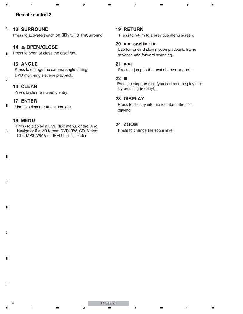
Remote control 2
13 SURROUNDPress to activate/switch off 2V/SRS TruSurround.
14Press to open or close the disc tray.
15 ANGLEPress to change the camera angle during DVD multi-angle scene playback.
16 CLEARPress to clear a numeric entry.
17 ENTERUse to select menu options, etc.
18 MENUPress to display a DVD disc menu, or the Disc Navigator if a VR format DVD-RW, CD, Video CD , MP3, WMA or JPEG disc is loaded.
19 RETURNPress to return to a previous menu screen.
20Use for forward slow motion playback, frame advance and forward scanning.
21Press to jump to the next chapter or track.
22Press to stop the disc (you can resume playback by pressing (play)).
23 DISPLAYPress to display information about the disc playing.
24 ZOOMPress to change the zoom level.
1 2 3 4

C
D
F
A
B
E
15
5 6 7 8
3. BASIC ITEMS FOR SERVICE3.1 CHECK POINTS AFTER SERVICING
Check points after servicing (DVD player)
To keep the product quality after servicing, confirm recommended check points shown below.
See the table below for the items to be checked regarding video and audio:
No. Procedure Check points
1 Confirm the firmware version on Service Mode. The version of the firmware must be latest.Update firmware to the latest one, if it is not the latest.
The customer complain must not be reappeared.Video, audio and operations must be normal.2
Confirm whether the customer complain has been solved. If the customer complain occurs with the specific disc, use it for the operation check.
The error rates must be less than 5.0e-4.3
Confirm playback error rates at the innermost and outermost tracks by using the following disc.DVD test disc (GGV1025)
4 Play back a DVD.(Menu operation, Title/chapter search)
Audio and operations must be normal.
5Play back a DVD.(Menu operation, Title/chapter search)
Video, audio and operations must be normal.
6 Check the appearance of the product. No scratches or dirt on its appearance after receiving it for service.
Items to be checked regarding video Item to be checked regarding audio
Block noise Distortion
Horizontal noise Noise
Dot noise Volume too low
Disturbed image (video jumpiness) Volume too high
Too dark Volume fluctuating
Too bright Sound interrupted
Mottled color
DV-300-K5 6 7 8
C
D
F
A
B
E
DV-300-K16
1 2 3 4
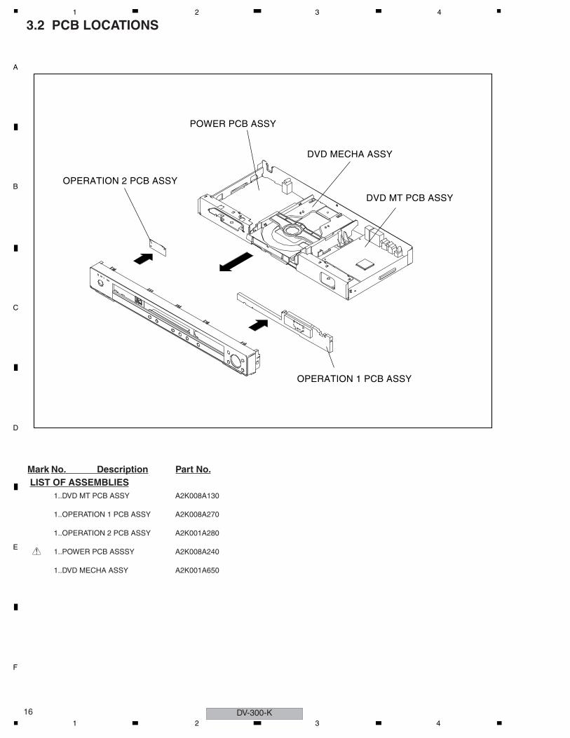
3.2 PCB LOCATIONS
OPERATION 1 PCB ASSY
OPERATION 2 PCB ASSY
POWER PCB ASSY
DVD MT PCB ASSY
DVD MECHA ASSY
Mark No. Description Part No.LIST OF ASSEMBLIES 1..DVD MT PCB ASSY A2K008A130 1..OPERATION 1 PCB ASSY A2K008A270 1..OPERATION 2 PCB ASSY A2K001A280 > 1..POWER PCB ASSSY A2K008A240 1..DVD MECHA ASSY A2K001A650
1 2 3 4

C
D
F
A
B
E
17
5 6 7 8
3.3 JIGS LIST
Service Remote Control Unit GGF1381 diagnosisName Jig No. Remarks
DVD Test Disc (DVD-Video,NTSC) GGV1025 Operation CheckDVD Test Disc (DVD-Video,PAL)CD Test Disc
GGV-1101STD-905
Operation CheckOperation Check
7 Jigs list
Lubricants and Glues list
Cleaning
Daifree GEM1036 (ZLX-ME413A) Refer to "9.3 06 DVD MECHA SECTION"
Grease GYA1001 (ZLB-PN397B) Refer to "9.3 06 DVD MECHA SECTION"
Grease GEM1018 Refer to "9.3 06 DVD MECHA SECTION"
Name Lubricants and Glues No. RemarkName Lubricants and Glues No. Remark
• Before shipping out the product, be sure to clean the following positions by using the prescribed cleaning tools:
Pickup leneses Cleaning liquid : GEM1004
Cleaning paper : GED-008
Position to be cleaned Cleaning tools RemarkPosition to be cleaned Cleaning tools Remark
DV-300-K5 6 7 8
C
D
F
A
B
E
DV-300-K18
1 2 3 4
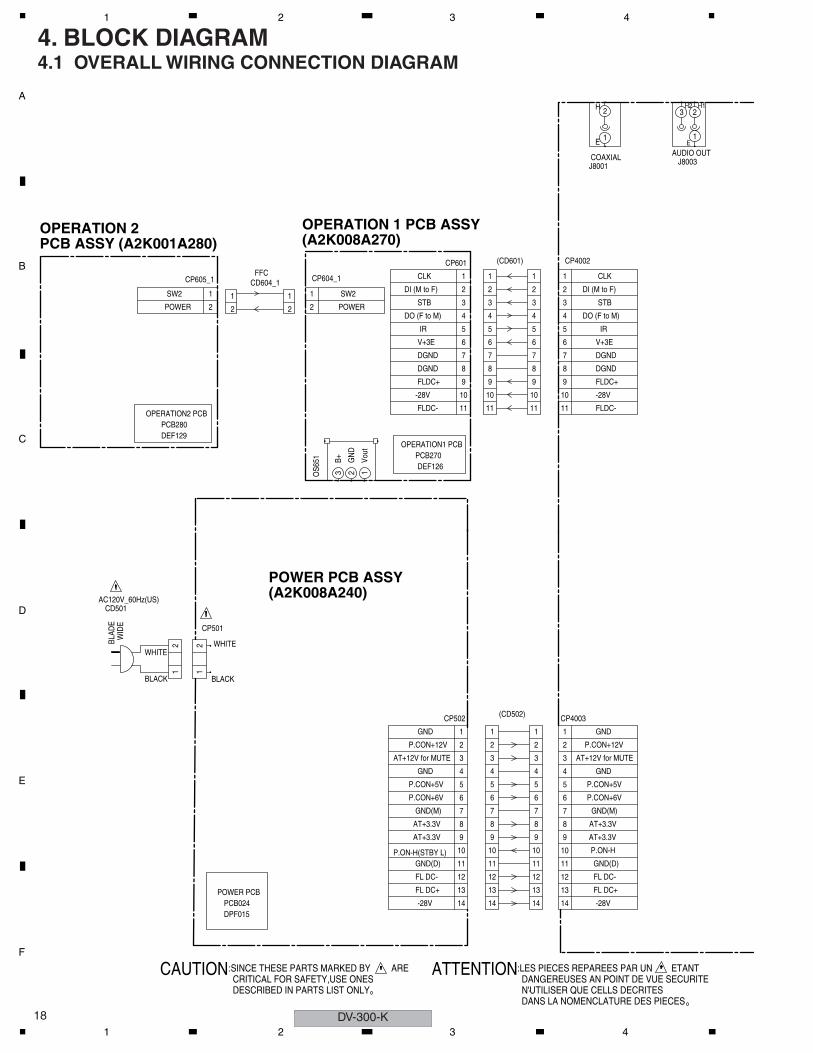
4. BLOCK DIAGRAM4.1 OVERALL WIRING CONNECTION DIAGRAM
2
1
CP604_1
2
1
CP605_1
11
10
9
8
7
6
5
4
3
2
1
11
10
9
8
7
6
5
4
3
2
1
14
13
12
11
10
9
8
7
6
4
5
3
2
1
CP502
14
13
12
11
10
9
8
7
6
4
5
3
2
1
CP4003
Vout
B+ GN
D
OS6
51
123
CP501
12BL
ADE
WID
E
BLACK
WHITE
21
CD501AC120V_60Hz(US)
:SINCE THESE PARTS MARKED BYCAUTIONDESCRIBED IN PARTS LIST ONLYCRITICAL FOR SAFETY,USE ONES
ARE
DANS LA NOMENCLATURE DES PIECESN'UTILISER QUE CELLS DECRITESDANGEREUSES AN POINT DE VUE SECURITE
:LES PIECES REPAREES PAR UN ETANTATTENTION
H
E
J8001COAXIAL
1
2H1H2
E
J8003AUDIO OUT
1
23
CD604_1SW2
POWER
SW2
POWER
FFC
2
1
2
1
OPERATION2 PCB
OPERATION1 PCB
DEF126PCB270
FLDC-
FLDC+
V+3E
-28V
DGND
DGND
DO (F to M)
DI (M to F)
IR
STB
CLK
DGND
DGND
FLDC+
-28V
FLDC-
DI (M to F)
V+3E
STB
DO (F to M)
IR
CLK
(CD601)
11
10
9
8
7
6
5
4
3
2
1
11
10
9
8
7
6
5
4
3
2
1
CP601 CP4002
DEF129PCB280
DPF015
P.ON-H(STBY L)
WHITE
BLACK
(CD502)
AT+3.3VAT+3.3V
AT+3.3V
14
13
14
13
12
11
10
9
8
7
6
5
4
3
2
1
12
11
10
9
8
7
6
5
4
3
2
1
PCB024POWER PCB
P.CON+12V
P.CON+5V
FL DC-
FL DC+
GND
GND
AT+12V for MUTE
P.CON+6V
-28V
GND(M)
GND(D)
GND
P.CON+5V
FL DC-
FL DC+
-28V
AT+3.3V
GND
P.CON+12V
AT+12V for MUTE
P.CON+6V
GND(M)
GND(D)
P.ON-H
OPERATION 2 PCB ASSY (A2K001A280)
OPERATION 1 PCB ASSY (A2K008A270)
POWER PCB ASSY(A2K008A240)
1 2 3 4

C
D
F
A
B
E
19
5 6 7 8
5
4
3
2
1
CP2302
6
5
4
3
2
1
CP2303
24
23
22
21
20
19
2
1
18
17
16
15
14
13
12
11
10
9
8
7
6
5
4
3
CP2301
OF PRINTING AND SUBJECT TO CHANGE WITHOUT NOTICETHE TIMETHIS INTERCONNECTION DIAGRAM IS THE LATEST ATNOTE:
H1H2
E
H1H2
E
J7302CVBS/Y/U/V
1
23
4
56
J7301S-VIDEO OUT
12
34
56
SW(GND)
LIMIT SW
SLD-
SLD+
SPD-
SPD+
GND
LOAD-
LOAD+
OPEN
CLOSE
DVD MT PCB
DMF089PCB130
B
A
VRCOM
VR780(CD)
VRF(RF_OUT)
SW1(DVD/CD)
C
VR650(DVD)
GND
LD_DVD(650)
LD_CD(780)
PD/GND
TRKG DRV
TRKG RTN
FOCS RTN
FOCS DRV
VCC
D
E
VS
F
GND
GND
NC
VRCOM
TRKG DRV
TRKG RTN
FOCS RTN
FOCS DRV
VCC
D
B
VR780(CD)
VRF(RF_OUT)
SW1(DVD/CD)
C
E
VS
F
GND
A
VR650(DVD)
GND
GND
LD_DVD(650)
LD_CD(780)
PD/GND
NC
DM-4PB
24
23
22
21
20
19
18
17
16
15
14
13
12
11
10
9
8
7
6
5
4
3
2
1
24
23
22
21
20
19
18
17
16
15
14
13
12
11
10
9
8
7
6
5
4
3
2
1
6
5
4
3
2
1 6
5
4
3
2
1
DRIVEDVD
OPTICAL PICK-UP
(LOADING MOTOR PCB)
DED021PCB610
CD2302
BCZ3B05M2603M
5
4
3
2
1
SW-2(CLOSE)
GND(SW)
SW-1(OPEN)
LOADING MOTOR(-)
LOADING MOTOR(-)
2H051602
SSS-28-5SW1
(SW PCB)
BCZ3B05
JCV9B12M2601
M2602
ESE22MH22SW2
M
M
2H061605CD2301
DED020PCB640
SPINDLE MOTOR(+)
SPINDLE MOTOR(-)
FEED MOTOR(-)
GND(SW)
FEED MOTOR(+)
PICK UO INNER LIMIT SWITCH
6
5
4
3
2
1DVD MT PCB ASSY (1/6 – 6/6)(A2K008A130)
DVD MECHA ASSY(A2K001A650)
DV-300-K5 6 7 8

C
D
F
A
B
E
DV-300-K20
1 2 3 4
4.2 OVERALL BLOCK DIAGRAM
P.C
ON
+12
V
AC
120V
FLD
C+
/-
X40
0127
MH
z
-28V
AT+
12V
for
mut
e
AT+
3.3V
P.C
ON
+6V
P.C
ON
+5V
PO
WE
RS
UP
PLY
DV
D L
OA
DE
R(D
M4)
IC23
01M
OTO
R D
RIV
ER
AM
5766
IC65
1F
IP D
RIV
ER
IC
PT
6315
IC40
02 E
EP
RO
MS
-24C
S08
AF
J-T
B-1
GE
IC80
03A
UD
IO A
MP
RC
4580
IDR
IC73
01V
IDE
O D
RIV
ER
6C
H IC
LA73
054-
TLM
-E
FIP
HN
V-0
8SS
44T
KE
Y
SE
RV
O
RF
SE
RV
O
IR
FP,
ST
B
CH
VID
EO
DA
C
AS
PD
IF
RE
SE
T
AU
DIO
_L,
AU
DIO
_R
AM
P_A
UD
IO_L
/R
LD_D
VD
,LD
_CD
IR10
8MH
zT
V E
ncod
erM
PE
G-1
/2/
JPE
GV
IDE
OD
EC
OR
DE
R
R
S_V
IDE
O
CO
AX
IAL
RF
V CO
L
OV
ER
AL
L B
LO
CK
DIA
GR
AM
IR R
EC
EIV
ER
(O
S65
1)R
OM
-N34
0TA
O
IC40
0416
Mbi
t FLA
SH
ES
29LV
160E
B-7
0TG
IC40
0564
Mbi
t SD
RA
MH
Y57
V64
1620
ET
P-7
-C
SD
A, S
CL
S
IC40
03R
ES
ET
ICR
3112
N29
1A-T
R-F
A
CV
BS
UY
AM
UT
E
IC40
01M
PE
G/M
ICO
N
BLO
CK
MT
1389
FE
/E-L
AU
DIO
CO
DE
C/
INT
ER
NA
L D
AC
1 2 3 4
C
D
F
A
B
E
21
5 6 7 8
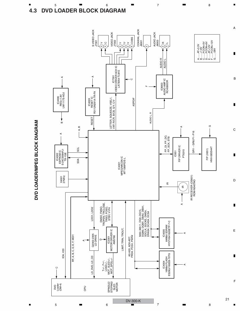
4.3 DVD LOADER BLOCK DIAGRAM
DV
D L
OA
DE
R/M
PE
G B
LO
CK
DIA
GR
AM
DV
DLo
ader
(DM
-4)
IC40
01M
PE
G/M
ICO
N IC
MT
1389
FE
/E-L
X40
0127
MH
z
IC40
02E
EP
RO
M IC
S-2
4CS
08A
FJ-
TB
-1G
E
SD
AS
CL
A, B
AIC
4006
RE
G+
1.8V
LM11
17S
-AD
JA
BIO
A, V
20
C
RF,
A, B
, C, D
, E, F
, MD
I1
IC40
03R
ES
ET
ICR
3112
N29
1A-T
R-F
AA
RE
SE
TLD
_DV
D, L
D_C
DQ
2302
-230
5LD
DR
IVE
LDO
1, L
DO
2
IC23
01M
OTO
R D
RIV
ER
ICA
M57
66
DM
SO
, FM
SO
, T
RO
PE
N, T
RC
LOS
E,
TR
SO
, FO
SO
, S
TB
Y, V
1P4
T+
/-, F
+/-
,LO
AD
+/-
, M
OT
_SLE
D+
/-,
MO
T_S
PD
L+/-
OP
U
SP
IND
LE/
ST
EP
ING
/S
LED
MO
TOR
LIM
IT, T
RIN
, TR
OU
T,
IC40
0416
Mbi
t FLA
SH
ES
29LV
160E
B-7
0TG
A
MA
0~M
A11
, DQ
0~D
Q15
,D
QM
0, D
QM
1, D
BA
0, D
BA
1,
SD
CLK
, SD
CK
E, D
WE
#,
DR
AS
#, D
CA
S#,
DC
S#
IC80
03A
UD
IO A
MP
ICR
C45
80ID
R
F
A D
A0-
A20
, AD
0-A
D7,
PR
D#,
PC
E#,
PW
R# IC
4005
64M
bit S
DR
AM
HY
57V
6416
20E
TP
-7-C
A
IC73
01V
IDE
O D
RIV
ER
6C
H IC
LA73
054-
TLM
-E
LET
TE
R, S
QU
EE
ZE
, VS
EL1
,I/X
P, R
/CR
, B/C
B, G
/Y, C
/V
43Y C
S-V
IDE
O J
AC
KJ7
301
35Y U
VID
EO
JA
CK
J730
2
62V C
VB
S
2CO
AX
IAL
JAC
KJ8
001
AS
PD
IF
32R L
AU
DIO
JA
CK
J800
3A
UD
IO R
AU
DIO
L
AU
DIO
L, R
GR
1 ~
GR
8,P
1~P
16
FIP
(V
651)
HN
V-0
8SS
44T
IR
IR R
EC
EIV
ER
(O
S65
1)R
OM
-N34
0TA
O
A
FP
_DI,
FP
_DO
, F
P_S
CK
, ST
BIR
IC65
1
FIP
DR
IVE
R IC
PT
6315
A
C
G
A B C D E F G
......
.AT
+3.
3V...
....+
1.8V
......
.P.C
ON
+5V
......
.P.C
ON
+6V
......
.AT
+12
V...
....P
.CO
N+
12V
......
.-28
V
DV-300-K5 6 7 8

C
D
F
A
B
E
P
OW
ER
BL
OC
K D
IAG
RA
M
DV-300-K22
1 2 3 4
4.4 POWER BLOCK DIAGRAM
SW
ITC
HIN
GT
RA
NS
T50
1
P.C
ON
SW
Q50
5
AC
IN
P.C
ON
+5V
AT+
3.3V
FL
DC
-
-28V
AT+
12V
for
mut
e
P.C
ON
+6V
P.C
ON
+12
V
P.O
N-H
FL
DC
+
Q51
5
P.C
ON
+5V
SW
Q51
0
P.C
ON
+12
V S
W
Q50
4
FL
+ P
.CO
N S
W
Q50
2
-28V
P.C
ON
SW
VO
LTA
GE
CT
LIC
501
KIA
431A
-AT
PH
OTO
CO
UP
LER
IC50
4P
S25
61A
L1-1
-V (
W)
PO
WE
R C
TL
IC50
2S
TR
-A61
31M
6V R
EG
IC50
3P
Q07
0XF
01S
ZH
1 2 3 4
C
D
F
A
B
E
23
5 6 7 8
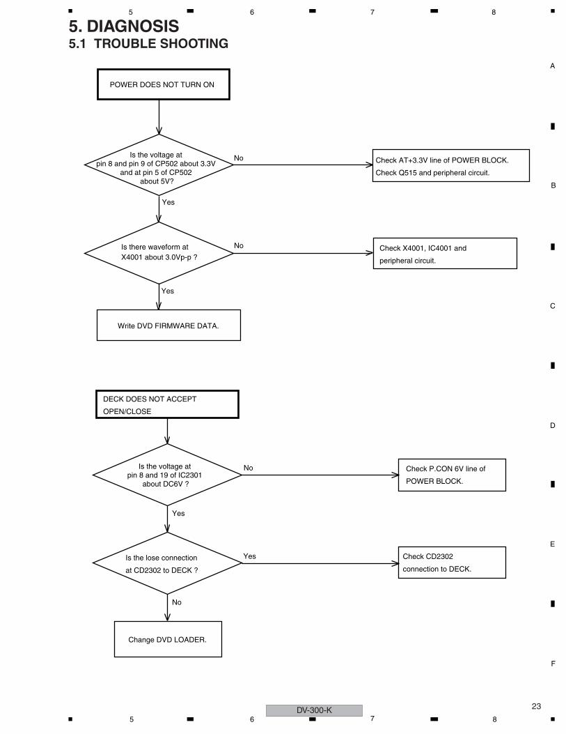
5. DIAGNOSIS5.1 TROUBLE SHOOTING
POWER DOES NOT TURN ON
Is the voltage at pin 8 and pin 9 of CP502 about 3.3V
and at pin 5 of CP502 about 5V?
No
Yes
NoIs there waveform atX4001 about 3.0Vp-p ?
Check X4001, IC4001 and
peripheral circuit.
Yes
Write DVD FIRMWARE DATA.
Check AT+3.3V line of POWER BLOCK.
Check Q515 and peripheral circuit.
No
Yes
No
DECK DOES NOT ACCEPT
OPEN/CLOSE
Check P.CON 6V line of
POWER BLOCK.
YesIs the lose connection
at CD2302 to DECK ?
Check CD2302
connection to DECK.
Change DVD LOADER.
Is the voltage at pin 8 and 19 of IC2301
about DC6V ?
DV-300-K5 6 7 8

C
D
F
A
B
E
DV-300-K24
1 2 3 4
DOES NOT LIGHT ON DISPLAY
Yes
Is the voltage at pin 13 and pin 43 of IC651
about 3V ?
Check AT+3.3V line of
POWER BLOCK.
No
Replace V651 or IC651.
NO PLAYBACK PICTURE OF AV
JACK
Is there video signal at pin 33
of IC7301 ?
Change IC7301.
No
Yes
No
Yes
Check J7302 and peripheral
circuit.
Is there a signal at pin 164 of
IC4001 ?
Check IC4001 and
peripheral circuit.
1 2 3 4

C
D
F
A
B
E
25
5 6 7 8
NO DIGITAL AUDIO ON
PLAYBACK OF COAXIAL JACK
Is there waveform at pin 2 of J8001
about 0.5Vp-p?
Check connection at RCA
Cable.
Yes
Yes
No
No
Change IC4001.
Is there waveform at pin 159 of IC4001
about 3.3Vp-p ?
Check Q8005 and
peripheral circuit.
NO ANALOG AUDIO ON
PLAYBACK
Is there AUDIO signal at pins 1 and 7
of IC8003 ?
Yes
Is there AUDIO signal at C8051
and C8053 ?
No
Check J8003 and peripheral
circuit.
Yes
No
Check AT pins 184 and
186 of IC4001.
Change IC8003.
DV-300-K5 6 7 8

C
D
F
A
B
E
DV-300-K26
1 2 3 4
Symptoms That May Occur When Any Of The Following ICs Is In FailureIC Symptoms
EEPROM(DVD MT PCB Assy : IC4002)
User's data cannot be stored in memory.The ID number is lost.
16M Flash ROM(DVD MT PCB Assy : IC4004)
The power cannot be turned on.Downloading of the firmware cannot be performed.
DVD IC(DVD MT PCB Assy : IC4001)
Any kind of symptoms (no power, a failure in any of the servo, video and audio systems, etc.) may be generated, because the DVD processing is performed by a single chip.
64M SDRAM(DVD MT PCB Assy : IC4005)
No power.Block noise is generated during playback.
1 2 3 4
C
D
F
A
B
E
27
5 6 7 8
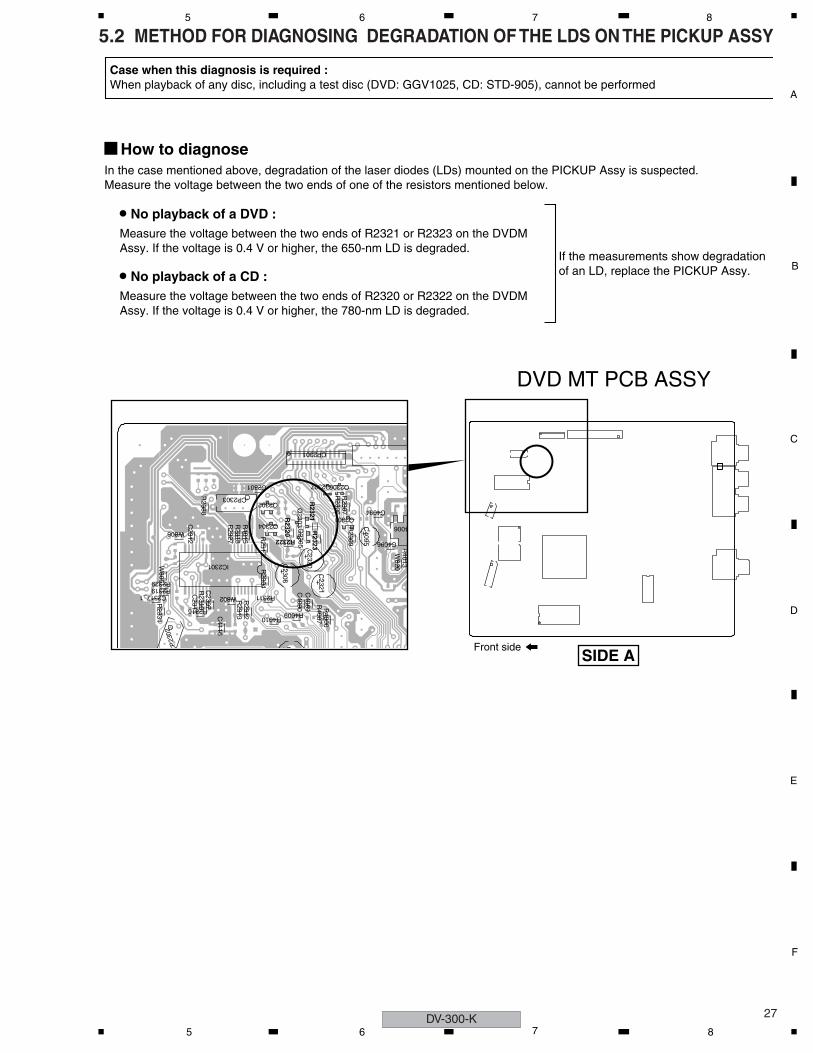
5.2 METHOD FOR DIAGNOSING DEGRADATION OF THE LDS ON THE PICKUP ASSY
C2317_1
W820
Q2307 Q2306
R2316
W805
W806
C2307
C2312
C2311
R2310
W802 R2313
R2312
R2304
R2327
R2318 R
2317
R2311
C2306
IC2301
C4116
C4006
C4096
C4095
C4094
R4013
R4015
C4089
C4090
C2301
CP2301
CP2303
CP
2302
C2321
C2320
R2309
R4009
R2306
R4006
R2307
R4007
R2323
R2321R
2320
R2322
R4010
R2338
R2331
R2319R2329
Q2303Q2304
Q2301
Q2305
Q2302
Case when this diagnosis is required : When playback of any disc, including a test disc (DVD: GGV1025, CD: STD-905), cannot be performed
How to diagnoseIn the case mentioned above, degradation of the laser diodes (LDs) mounted on the PICKUP Assy is suspected.Measure the voltage between the two ends of one of the resistors mentioned below.
Measure the voltage between the two ends of R2321 or R2323 on the DVDM Assy. If the voltage is 0.4 V or higher, the 650-nm LD is degraded.
No playback of a DVD :
Measure the voltage between the two ends of R2320 or R2322 on the DVDM Assy. If the voltage is 0.4 V or higher, the 780-nm LD is degraded.
No playback of a CD :
If the measurements show degradation of an LD, replace the PICKUP Assy.
SIDE AFront side
DVD MT PCB ASSY
DV-300-K5 6 7 8
C
D
F
A
B
E
DV-300-K28
1 2 3 4
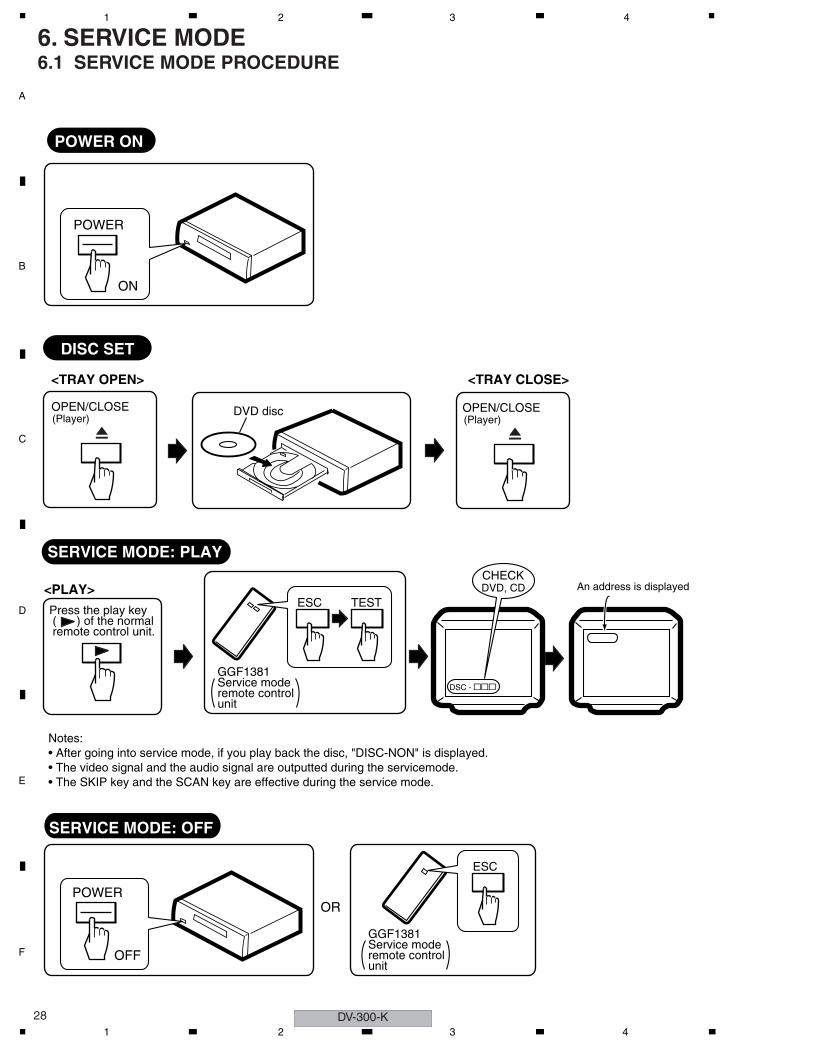
6. SERVICE MODE6.1 SERVICE MODE PROCEDURE
POWER ON
DSC - &&&
GGF1381Service moderemote controlunit
GGF1381Service moderemote controlunit
<TRAY OPEN> <TRAY CLOSE>
OPEN/CLOSE(Player)
OPEN/CLOSE
Press the play key ( ) of the normal remote control unit.
(Player)
An address is displayed
OR
ESC
<PLAY>ESC TEST
CHECKDVD, CD
DVD disc
POWER
ON
OFF
POWER
DISC SET
Notes:• After going into service mode, if you play back the disc, "DISC-NON" is displayed.• The video signal and the audio signal are outputted during the servicemode.• The SKIP key and the SCAN key are effective during the service mode.
SERVICE MODE: PLAY
SERVICE MODE: OFF
1 2 3 4

C
D
F
A
B
E
29
5 6 7 8
6.2 SERVICE MODE IN
Service Mode Functional Specification1 Service mode entry
In the power ON state, press the [ESC] (A8-5F) key and [TEST / RANDOM] (A8-5E) key in order of the Service mode remote control unit. • Light the all FL and LEDs.• OSD displays test mode.
Note:* When pressing the keys of something, the FL displays "NO DISC" and the LED lighting disappears.
2 Release the Service mode• Turn off the power.• Press the [ESC] (A8-5F) key of the remote control unit.
3 LD ONDVD : Press the [TEST] (A8-5E) and [1] (A8-01) keys in order, and turn on the laser diode (650n).CD : Press the [TEST] (A8-5E) and [4] (A8-04) keys in order, and turn on the laser diode (780n).
DV-300-K5 6 7 8
C
D
F
A
B
E
DV-300-K30
1 2 3 4
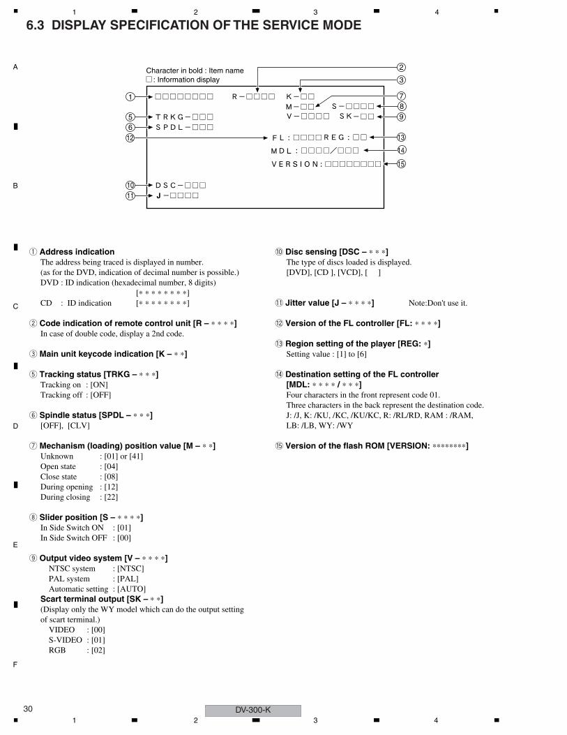
6.3 DISPLAY SPECIFICATION OF THE SERVICE MODE
Character in bold : Item name: Information display
1
56
1011
89
3
2
12
15
13
14
1 Address indicationThe address being traced is displayed in number. (as for the DVD, indication of decimal number is possible.)DVD : ID indication (hexadecimal number, 8 digits)
[∗ ∗ ∗ ∗ ∗ ∗ ∗ ∗]CD : ID indication [∗ ∗ ∗ ∗ ∗ ∗ ∗ ∗]
2 Code indication of remote control unit [R – ∗ ∗ ∗ ∗]In case of double code, display a 2nd code.
3 Main unit keycode indication [K – ∗ ∗]
5 Tracking status [TRKG – ∗ ∗ ∗]Tracking on : [ON]Tracking off : [OFF]
6 Spindle status [SPDL – ∗ ∗ ∗][OFF], [CLV]
7 Mechanism (loading) position value [M – ∗ ∗]Unknown : [01] or [41]Open state : [04]Close state : [08]During opening : [12]During closing : [22]
8 Slider position [S – ∗ ∗ ∗ ∗]In Side Switch ON : [01]In Side Switch OFF : [00]
9 Output video system [V – ∗ ∗ ∗ ∗]NTSC system : [NTSC]PAL system : [PAL]Automatic setting : [AUTO]
Scart terminal output [SK – ∗ ∗] (Display only the WY model which can do the output settingof scart terminal.)
VIDEO : [00] S-VIDEO : [01]RGB : [02]
0 Disc sensing [DSC – ∗ ∗ ∗]The type of discs loaded is displayed.[DVD], [CD ], [VCD], [ ]
- Jitter value [J – ∗ ∗ ∗ ∗] Note:Don't use it.
= Version of the FL controller [FL: ∗ ∗ ∗ ∗]
~ Region setting of the player [REG: ∗]Setting value : [1] to [6]
! Destination setting of the FL controller[MDL: ∗ ∗ ∗ ∗ / ∗ ∗ ∗]Four characters in the front represent code 01.Three characters in the back represent the destination code.J: /J, K: /KU, /KC, /KU/KC, R: /RL/RD, RAM : /RAM, LB: /LB, WY: /WY
@ Version of the flash ROM [VERSION: ∗∗∗∗∗∗∗∗]
7
1 2 3 4
C
D
F
A
B
E
31
5 6 7 8
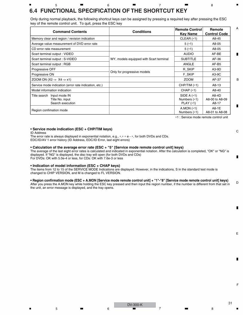
6.4 FUNCTIONAL SPECIFICATION OF THE SHORTCUT KEY
• Service mode indication (ESC + CHP/TIM keys)ID AddressThe error rate is always displayed in exponential notation, e.g., ∗.∗ ∗ e - ∗, for both DVDs and CDs.EDC/ID/AV 1 error history (ID Address, EDC/ID Error, last eight errors)
• Calculation of the average error rate (ESC + "5" [Service mode remote control unit] keys)The average of the last eight error rates is calculated and indicated in exponential notation. After the calculation is completed, "OK" or "NG" is displayed. If "NG" is displayed, the disc tray will open (for both DVDs and CDs)For DVDs: OK with 5.0e-4 or less, for CDs: OK with 7.6e-3 or less
• Indication of model information (ESC + CHAP keys)The items from 12 to 15 of the SERVICE MODE Indications are displayed. However, in the indications, S in the standard test mode is changed to CHIP VERSION, and M is changed to FL VERSION.
• Region confirmation mode (ESC + A.MON [Service mode remote control unit] + "1"-"8" [Service mode remote control unit] keys)After you press the A.MON key while holding the ESC key pressed and then input the region number, if the number is different from that set in the unit, an error message is displayed, and the tray opens.
Command Contents ConditionsRemote Control
Key NameRemote
Control CodeMemory clear and region / revision indication CLEAR (∗1) A8-45
Average value measurement of DVD error rate 5 (∗1) A8-05
CD error rate measurement 5 (∗1) A8-05
Scart terminal output : VIDEO
WY, models equipped with Scart terminal
AUDIO AF-BE
Scart terminal output : S-VIDEO SUBTITLE AF-36
Scart terminal output : RGB ANGLE AF-B5
Progressive OFFOnly for progressive models
R_SKIP A3-9D
Progressive ON F_SKIP A3-9C
ZOOM ON (X2 -> X4 -> x1) ZOOM AF-37
Service mode indication (error rate indication, etc.) CHP/TIM (∗1) A8-13
Model information indication CHAP (∗1) A8-40
Title search Input mode INTitle No. inputSearch execution
SIDE A (∗1)Numbers (∗1)
PLAY (∗1)
A8-4DA8-00 to A8-09
A8-17
Region confimation modeA.MON (∗1)
Numbers (∗1)A8-1E
A8-01 to A8-08
Only during normal playback, the following shortcut keys can be assigned by pressing a required key after pressing the ESC key of the remote control unit. To quit, press the ESC key
∗1 : Service mode remote control unit
DV-300-K5 6 7 8
C
D
F
A
B
E
DV-300-K32
1 2 3 4
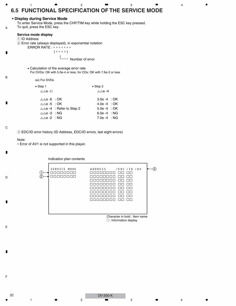
6.5 FUNCTIONAL SPECIFICATION OF THE SERVICE MODE• Display during Service Mode
To enter Service Mode, press the CHP/TIM key while holding the ESC key pressed.To quit, press the ESC key.
Service mode display1 ID Address2 Error rate (always displayed), in exponential notation
ERROR RATE : ∗ ∗ ∗ ∗ ∗ ∗ ∗ ( ∗ ∗ ∗ ∗ )
• Calculation of the average error rate For DVDs: OK with 5.0e-4 or less, for CDs: OK with 7.6e-3 or less
3 EDC/ID error history (ID Address, EDC/ID errors, last eight errors)
Note:∗ Error of AV1 is not supported in this player.
Number of error
Indication plan contents
Character in bold : Item name: Information display
12
3
ex) For DVDs
• Step 1
%%e -&
%%e -6 : OK%%e -5 : OK%%e -4 : Refer to Step 2%%e -3 : NG%%e -2 : NG
• Step 2
%%e -4
3.0e -4 : OK4.0e -4 : OK5.0e -4 : OK6.0e -4 : NG7.0e -4 : NG
1 2 3 4

C
D
F
A
B
E
33
5 6 7 8
7. DISASSEMBLY7.1 EXTERIOR SECTION
1. REMOVAL OF MECHANICAL PARTSAND P.C. BOARDS
1-1:TOP CABINET/FRONT CABINET/OPERATION PCB(Refer to Fig. 1-1)
1. Remove the 5 screws 1.2. Remove the Top Cabinet in the direction of arrow (A).3. Disconnect the following connector: (CP4002).4. Unlock the 4 supports 2.5. Remove the Front Cabinet in the direction of arrow (B).6. Remove the 10 screws 3.7. Remove the Operation PCB in the direction of arrow (C).
1. Short circuit the position shown in Fig. 1-3 using asoldering iron. If you remove the DVD Deck with nosoldering, the Laser may be damaged.
2. Disconnect the following connectors:(CP2301, CP2302 and CP2303).
3. Remove the 4 screws 1.4. Remove the DVD Deck in the direction of arrow.
1-3: DVD DECK (Refer to Fig. 1-3)
Fig. 1-3
NOTE
1. Before your operation, please read “PREPARATION OFSERVICING”.
2. Use the Lead Free solder.3. Manual soldering conditions
• Soldering temperature: 320 ± 20˚C• Soldering time: Within 3 seconds• Soldering combination: Sn-3.0Ag-0.5Cu
4. When Soldering/Removing of solder, use the drawingequipment over the Pick Up Unit to keep the Flux smokeaway from it.
5. When installing the DVD Deck, remove all the solderingon the short circuit position after the connection of Pick Up PCB and DVD MT PCB connector.
1-4: DVD MT PCB (Refer to Fig. 1-4)
1. Remove the 4 screws 1.2. Remove the 4 screws 2.3. Remove the DVD MT PCB in the direction of arrow.
Fig. 1-4
11
2
2
2
DVD MT PCB
2
DVD Deck
1
1
11
Short circuit using asoldering iron.
Pick Up PCB
1-2: POWER PCB (Refer to Fig. 1-2)
1. Disconnect the following connector: (CP502).2. Remove the 4 screws 1.3. Remove the Power PCB in the direction of arrow.
Fig. 1-1
Fig. 1-2
1
1
Power PCB1
1
1
(B)
(A)
1
1
1
1
Top Cabinet
Front Cabinet
3
2
(C)
(C)
Operation PCB
Operation 2 PCB
2
2
2
3
33
33
33
3
3
11
DV-300-K5 6 7 8

C
D
F
A
B
E
DV-300-K34
1 2 3 4
7.2 DVD DECK SECTION
2. REMOVAL OF DVD DECK PARTS
2-1: TRAY (Refer to Fig. 2-1-A)
METHOD AT NO POWER SUPPLY)
Tray.
1. Set the Tray opened. (Refer to the DISC REMOVAL
2. Unlock the 2 supports 1 and draw it while sagging the
Fig. 2-1-A
Tray
Push to Sag
Push to Sag
Loader Ass'y
1
NOTE
1. In case of the Tray installation, install them as the circledsection of Fig. 2-1-B so that the each markers are met.
2-2: TRAVERSE ASS'Y (Refer to Fig. 2-2-A)
1. Remove the screw 1.2. Unlock the 2 supports 2.3. Remove the Insulator (R) from the Loader Sub Ass'y.4. Remove the Traverse Ass'y.
Fig. 2-2-A
Tray
Loader Ass'y
Fig. 2-1-B
Insulator (R)
NOTE
1. Disassemble only the DVD DECK PARTS parts listedhere. Minute adjustments are needed if the disassemblyis done. If the repair is needed except listed parts,replace the DVD MECHA ASS'Y.
NOTE
1. In case of the Traverse Ass'y, install it from (1) to (4) in
2. In case of the Traverse Ass'y installation, hook the wireorder. (Refer to Fig. 2-2-B)
on the Loader Ass'y as shown Fig. 2-2-C.
1
Traverse Ass'y
Loader Sub Ass'y
Fig. 2-2-BCheck Lock
Traverse Ass'y
Rack Loading
Loader Ass'y (Bottom Side)
Holder Traverse
Fig. 2-2-C
Loader Ass'y
Check Hook
Loading Belt
Loading Sub Ass'y
Gear Pulley
1
2-3: LOADING MOTOR PCB ASS'Y/ LOADING BELT(Refer to Fig. 2-3-A)
1. Remove the Loading Belt.2. Remove the screw 1.3. Remove the Loading Motor PCB Ass'y.4. Remove the 2 screws 2.5. Remove the Loading Motor.6. Remove the Gear Pulley.
Fig. 2-3-A
Loading Motor PCB Ass’y
• Screw Torque: 2.0 ± 0.3kgf•cm
• Screw Torque: 2.5 ± 0.3kgf•cm (Screw 1)• Screw Torque: 1.0 ± 0.3kgf•cm (Screw 2)
22
Loading Motor
2
2
1 2 3 4
C
D
F
A
B
E
35
5 6 7 8
BROWN (1)
WHITE (2)
NOTE
1. In case of the Pulley Motor installation, check if the value
2. When installing the wire of the Loading Motor PCB Ass'y,
3. When installing the Loading Motor PCB Ass'y, install it
4. In case of the Loading Motor PCB Ass'y installation, hook
of the Fig. 2-3-B is correct.
install it correctly as Fig. 2-3-C.Manual soldering conditions• Soldering temperature: 320 ± 20˚C• Soldering time: Within 3 seconds• Soldering combination: Sn-3.0Ag-0.5Cu
correctly as Fig. 2-3-D.
the wire on the Loader Sub Ass'y as shown Fig. 2-3-E.
Fig. 2-3-B
7.0 ± 0.1mm
Safety surface for pressingof the insert.
Loading Motor
Pulley Motor
Check HookLoading Motor PCB Ass’y
Loading Motor PCB Ass’yFig. 2-3-C
Fig. 2-3-E
Check Hook
Fig. 2-3-D
Rack Loading
BA
The Lever should be positionbetween A and B.
Check Hook
Rack Loading
1
Loader Sub Ass’y
Gear Main
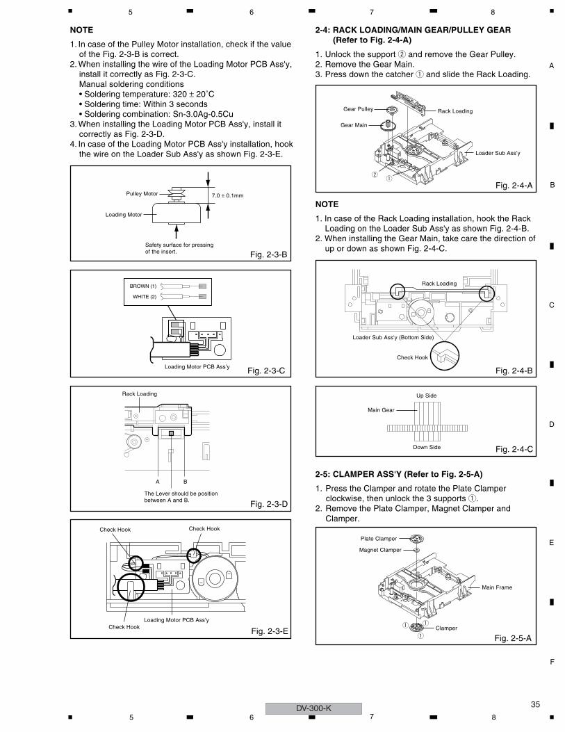
2-4: RACK LOADING/MAIN GEAR/PULLEY GEAR(Refer to Fig. 2-4-A)
1. Unlock the support 2 and remove the Gear Pulley.2. Remove the Gear Main.3. Press down the catcher 1 and slide the Rack Loading.
Gear Pulley
2
Fig. 2-4-A
NOTE
1. In case of the Rack Loading installation, hook the Rack
2. When installing the Gear Main, take care the direction ofLoading on the Loader Sub Ass'y as shown Fig. 2-4-B.
up or down as shown Fig. 2-4-C.
Fig. 2-4-B
Rack Loading
Check Hook
Fig. 2-4-C
Main Gear
Up Side
Down Side
2-5: CLAMPER ASS'Y (Refer to Fig. 2-5-A)
clockwise, then unlock the 3 supports 1.1. Press the Clamper and rotate the Plate Clamper
2. Remove the Plate Clamper, Magnet Clamper and Clamper.
Plate Clamper
Magnet Clamper
Fig. 2-5-A
Main Frame
Clamper1
11
Loader Sub Ass'y (Bottom Side)
DV-300-K5 6 7 8

C
D
F
A
B
E
DV-300-K36
1 2 3 4
Holder Traverse
Insulator (F)
Traverse Ass'y
Insulator (F)
Insulator (R)
NOTE
1. In case of the Clamper Ass'y installation, install correctlyas Fig. 2-5-B.
Fig. 2-5-B
Plate Clamper
Clamper
2-6: HOLDER TRAVERSE/INSULATOR (F)/INSULATOR
1. Remove the Holder Traverse.2. Remove the 2 Insulator (F).3. Remove the Insulator (R).
Fig. 2-6-A
(R) (Refer to Fig. 2-6-A)
NOTE
1. In case of the Insulator (F) installation, install correctly as Fig. 2-6-B.
Fig. 2-6-B
Traverse Holder
Insulator (F)
2-7: SWITCH PCB ASS'Y/GEAR MIDDLE/GEAR FEED/RACK FEED ASS'Y/FEED MOTOR (Refer to Fig. 2-7-A)
1. Unlock the support 1.2. Remove the Gear Middle.3. Remove the screw 2.4. Remove the Rack Feed Ass'y.5. Remove the screw 3.6. Remove the Switch PCB Ass'y.7. Remove the screw 4.8. Remove the Gear Feed.9. Remove the 2 screws 5.10. Remove the Feed Motor.11. Remove the Gear Motor.
3
Gear Middle
Gear Motor
Feed Motor
• Screw Torque: 1.3 ± 0.3kgf•cm (Screw 2)• Screw Torque: 3.0 ± 0.3kgf•cm (Screw 3)• Screw Torque: 1.0 ± 0.3kgf•cm (Screw 4, 5)
Switch PCB Ass'y
2
4
Rack Feed Ass'y
Gear Feed
5
Fig. 2-7-A
Traverse Ass'y51
NOTE
1. When installing the Rack Feed Ass'y, push both ends to
2. In case of the Gear Motor installation, check if the value
3. When installing the wire of the Switch PCB Ass'y, install
4. After the assembly of the Traverse Ass'y, hook the wire
align the teeth as shown Fig. 2-7-B. Then install it.
of the Fig. 2-7-C is correct.
it correctly as Fig. 2-7-D.Manual soldering conditions• Soldering temperature: 320 ± 20˚C• Soldering time: Within 3 seconds• Soldering combination: Sn-3.0Ag-0.5Cu
on the Traverse Ass'y as shown Fig. 2-7-E.
[OK] [NG]
Fig. 2-7-B
Rack Feed Ass'y
PushPush
Fig. 2-7-C
8.0 ± 0.2mm
Safety surface for pressingof the insert.
Feed Motor
Gear Motor
Check Lock
Pickup lenesesGEM1004GED-008
1 2 3 4

C
D
F
A
B
E
37
5 6 7 8
[ 24 pin FFC ]
shown from Fig. 2-8.
2-8: FFC WIRE HANDLING
1. When installing the FFC, fold it correctly and install it as
positions for the FFC.1. Do not make the folding lines except the specified
NOTE
Fig. 2-8
Traverse Ass'y
• Loosen the wire in the direcion of the arrow.
Check Hook
Fig. 2-7-E
~ FEED MOTOR ~
WHITE (4)
BROWN (3)
~ SPINDLE MOTOR ~
YELLOW (2)
GREEN (1)
Fig. 2-7-D
Switch PCB Ass'y
Printing Surface Fold
79 ± 1 mm
Reinforcement Plate
To Pick Up PCB
DV-300-K5 6 7 8

C
D
F
A
B
E
DV-300-K38
1 2 3 4
8. EACH SETTING AND ADJUSTMENT8.1 ADJUSTMENT
8.2 RE-WRITE FOR DVD FIRMWARE
There is no information to be shown in this chapter.
1. PurposeAfter replacing the DVD MT PCB Assy, be sure to update the firmware to the latest version. The firmware of the Assy for service may not be the latest.
3. Procedures for updating the firmwareHow to update:1 Turn on the main unit and open the disc tray.2 Place the disc for updating in the disc tray and close the tray.3 Press the PLAY button.
4 Updating of the firmware is completed.
2. Procedures for creating the disc for updatingNecessary tools:1 PC with a CD-R/CD-RW drive2 Blank CD-R or CD-RW3 Firmware file (∗∗∗∗∗.BIN)
How to create:1 Start up the program for writing to CD.2 Load a blank disc in the CD-R/CD-RW drive.3 Enter "PIONEER" as the volume label.4 Select the .BIN file.5 Write the latest version of the firmware in ISO 9660 format.
While the screen shown at left is being displayed, updating is in progress.DO NOT TURN OFF THE POWER DURING UPDATING.
When the screen with the Pioneer logo is displayed, updating is completed.The time required for updating is about 2 minutes.
1 2 3 4
C
D
F
A
B
E
39
5 6 7 8
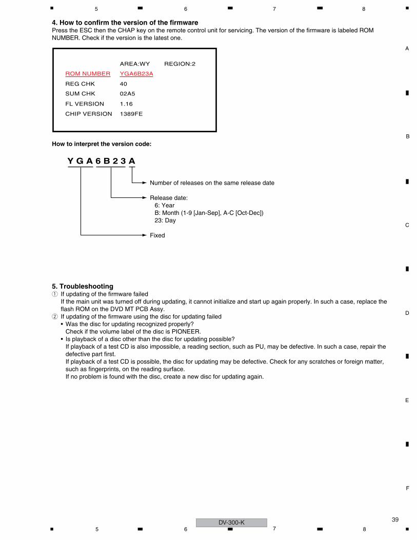
4. How to confirm the version of the firmwarePress the ESC then the CHAP key on the remote control unit for servicing. The version of the firmware is labeled ROM NUMBER. Check if the version is the latest one.
5. Troubleshooting1 If updating of the firmware failed
If the main unit was turned off during updating, it cannot initialize and start up again properly. In such a case, replace the flash ROM on the DVD MT PCB Assy.
2 If updating of the firmware using the disc for updating failed• Was the disc for updating recognized properly?
Check if the volume label of the disc is PIONEER.• Is playback of a disc other than the disc for updating possible?
If playback of a test CD is also impossible, a reading section, such as PU, may be defective. In such a case, repair the defective part first.If playback of a test CD is possible, the disc for updating may be defective. Check for any scratches or foreign matter, such as fingerprints, on the reading surface.If no problem is found with the disc, create a new disc for updating again.
YGA6B23A
AREA:WY
40
02A5
1.16
1389FE
ROM NUMBER
REGION:2
REG CHK
SUM CHK
FL VERSION
CHIP VERSION
Y G A 6 B 2 3 A
How to interpret the version code:
Number of releases on the same release date
Release date:6: YearB: Month (1-9 [Jan-Sep], A-C [Oct-Dec])23: Day
Fixed
DV-300-K5 6 7 8

C
D
F
A
B
E
DV-300-K40
1 2 3 4
9. EXPLODED VIEWS AND PARTS LIST
9.1 PACKING SECTION
Parts marked by "NSP" are generally unavailable because they are not in our Master Spare Parts List.The mark found on some component parts indicates the importance of the safety factor of the part.Therefore, when replacing, be sure to use parts of identical designation.Screws adjacent to mark on product are used for disassembly. For the applying amount of lubricants or glue, follow the instructions in this manual.(In the case of no amount instructions, apply as you think it appropriate.)
NOTES:
9
11
11
10
13
11
11
12
1 2 3 4

C
D
F
A
B
E
41
5 6 7 8
PACKING SECTION parts List
Mark No. Description Part No.
1 • • • • • •
2 Audio/Video Cable 06CPBA2006
3 Remote Control 07650KY060
4 Package Pad 792WHAA237
5 • • • • • •
NSP 6 Guarantee Card J2G00202B
7 Operating Instructions J2K00801A
(English)
8 Operating Instructions J2K00810A
(French)
9 Polyethylene Bag,Instruction JB5KD300
10 Gift Sheet 791WHAA183
11 Package 792WHAA227
12 Gift Box 793WCDD454
13 Polyethylene Bag,INSTA5 791WHAA040
DV-300-K5 6 7 8

C
D
F
A
B
E
DV-300-K42
1 2 3 4
9.2 EXTERIOR SECTION
B
B
A
A
C
C
CONTACT SIDE
NON-CONTACT SIDE
19
19
19
1317
17
4
1818
18
18
10
12
3
14 22
21
33
29
32
27
28
12
15
15
12
2121
2121
21
21
2
14
22
12
2318 18
18
18
1
11
11
25
2420
5
17
17
19
19
26
7
1 2 3 4

C
D
F
A
B
E
43
5 6 7 8
EXTERIOR SECTION parts List
Mark No. Description Part No.
1 DVD MT PCB Assy A2K008A130
2 OPERATION 1 PCB Assy A2K008A270
3 OPERATION 2 PCB Assy A2K001A280
> 4 POWER PCB Assy A2K008A240
5 DVD MECHA ASSY A2K001A650
> 6 Cord, AC Bush 120Q618902
NSP 7 Plate,Bottom 702WSAA192
8 • • • • • •
NSP 9 Sheet,Caution 726000A140
10 Plate,Cover power 755WPAA031
11 Holder,FFC 761WPA0396
12 Cushion,Leg VEB1349
13 Cabinet,Top 702WSB0115
14 Spring Earth 743WKAA015
15 Cushion (15x20x16) 8965TS101B
16 • • • • • •
17 Screw,Tap Tite(S)-Bind Wash. 816423063U
18 Screw,Tap Tite(S) (3x5.5) 8107D3055U
19 Screw,Tap Tite(B) (3x6.0) 8109K3060S
20 Screw,Tap Tite(B)Pan (3x6) 810913060U
21 Screw,Tap Tite(P) (2.6x8) 811022680U
22 Screw,Tap Tite(P) Bind WH7 8110I2680U
NSP 23 Sheet,Jack 1 722631A203
NSP 24 Sheet,Jack 2 722631A219
NSP 25 Sheet,Jack 3 722631A220
NSP 26 Sheet Caution 7250000597
27 Front Cabi Assy 7A701A911A
28 Flap, DVD 712WPDA079
29 Spring, Flap-DVD 743WKA0052
30 Cord Connector (CD502) 06CU2E3301
31 Cord Jumper (CD601) 122H0B1003
NSP 32 Energy Star Label 7230007965
33 Flat Cable (CD604) W9L6020038
DV-300-K5 6 7 8

C
D
F
A
B
E
DV-300-K44
1 2 3 4
9.3 06 DVD MECHA SECTION
Applying positions AA, AB and AC for the grease are displayed for this section.Check if the correct grease is applied for each position.
NOTE:CLASS MARK
GREASE AA
AB
PART NO.
GEM1018
GYA1001
ACGEM1036
Cannot supply separately.If the repair is needed, replace the LOADER SUB ASS'Y.
PCB610(LOADING MOTOR PCB ASS'Y)
CD2302
Do not replace the parts. Because, minute adjustments are needed if this condition is disassembled further more.If the repair is needed, replace the DVD MECHA ASS'Y.
(SW PCB ASS'Y)
AB
AB
AB
AA
AB
AB
AB
SW1
PCB640
CD2001
SW2
CD2301
AC
AC
AB Lubricating OilGYA1001
DaifreeGEM1036
Pickup lenesesGEM1004GED-008
GreaseGEM1018
Note :
Lubricating OilGYA1001
1 2 3 4
C
D
F
A
B
E
45
5 6 7 8
06 DVD MECHA SECTION parts List
Mark No. Description Part No.
1 • • • • • •
2 Gear,Middle 92P100117A
3 Loading Motor 1515S98004
4 Pulley,Motor 92P100097A
5 FEED Motor 1515S98004
6 Cord Jumper (24P)(CD2001) 122J4O2202
7 Cord Jumper (CD2302) 122H051602
8 Insulator (F) 92P200013A
9 Belt,Loading 92P200015A
10 Insulator (R) 92P200016A
11 Frame,main 92P100119A
12 Tray (R) 92P100151A
13 Holder ,Traverse 92P100125A
14 Gear,Pulley 92P100123A
15 Gear,Main 92P100124A
16 Gear,Feed 92P100116A
17 • • • • • •
18 Plate, Clamper 92P000023A
19 LOADER SUB ASSY (R) 92AAA0024A
20 Clamper 92P100122A
21 Screw,Pan (M1.7x3 P3) 814011730U
22 Screw,Pan (M1.7x2.3 P3) 814011723U
23 Rack,Loading 92P100121A
24 Gear,Motor 92P100088A
25 Feed Rack Assy 92AAA0017A
26 Screw,T-Tite(B) (M1.7x5.0 P3) 813381750U
27 Screw,Gear Feed 92P700007A
28 Cord Jumper (CD2301) 122H061605
29 Switch (SW1) 0515S32003
30 Push Switch (SW2) 0500101036
31 Screw,Tap Tite(P) (2.6x8) 811022680U
32 Sems.Tap Tite(P) (2x8) 816112080U
33 Screw (Bind 2x8) 811022080U
34 DVD MECHA ASSY A2K001A650
DV-300-K5 6 7 8

C
D
F
A
B
E
13P
CH
C40
46
BC
4057
C40
38
C40
47 1000
6.3V
YK_P
IC4001MT1389FE
MPEG/MIC
1881891901
0 81 82 83
OF NOTE:THIS
V+3A
AD7
A17
A0SD
ASC
L
C
0.0
2.0
RFG
ND
18AL
E (P
U)
AD7
IOA0
(PU
)A1
7 (P
U)
ADAC
VDD
2(A)
3.3
3.3
ADAC
VDD
1(A)
ALF(
CTR
)/GPI
O(A
)
1.0
1.7 0
18
00
3.3
1
DV-300-K46
1 2 3 4
10. SCHEMATIC DIAGRAM10.1 DVD MT PCB ASSY (1/6)
C4035
390P CH
C40
32
0.47
B
C40
27
22P
CH
C40
33
11P
CH
C40
310.
047
B
C40
23 0.1
B
C40
10
220P
CH
C41
03
0.00
22B
C40
90
0.1
BC
4101
270P
CH
C4005
0.1 B
C40
37C
4036
0.1
B
C40
16
0.1
B
C40
240.
1B
C40
220.
033
B
C40
260.
1B
C40
280.
1B
C40
290.
047
B
C40
340.
1B
C40
190.
1B
C40
200.
1B
C40
180.
1B
C40
250.
001
B
C40010.1 B
C4011 1 BC4012 1 BC4013 1 BC4014 1 B
C4006 0.1 B
C40030.1 B
C4002 0.1 B
C40070.1 B
C41
02
270P
CH
C4088 1 B
C40
89
0.01
5B
C40
30 1025
VKA
_P
R4022
750K
R40
2582
R40
20
100K R4024
100K
R4001 33
R40
03
680K
R40
1510
K
R40
1410
K
R40
1815
K
R40
02
10K
R40
04
10K
R4009 13K +-1%R4010 13K +-1%
R4007 8.2K +-1%R4006 13K +-1%
R40
61
10K
TP4008TP4009
TP4010TP4011
TP40
29
IC40
02S-
24C
S08A
FJ-T
B-1G
E
EEPR
OM
IC
1234
5 6 7 8
X4001100GT02720
27MHz
19192193194195196197198199200201202203204205206207208209210211212213214215216
110
1112
1314
1516
1718
192
2021
2223
2425
2627
2829
330
3132
3334
3536
3738
394
4041
4243
4445
4647
4849
550
5152
5354
55 56 57 58 59
6
60 61 62 63 64 65 66 67 68 69
7
70 71 72 73 74 75 76 77 78 79
8
8
9
MEASURED WITH THE DIGITAL TESTER DURING PLAYBACK.NOTE:THE DC VOLTAGE EACH PART WAS
V1P4
V+1R
8
MDI1V20
STBYABCDEF V+3
LDO1LDO2
DMSOFMSO
TRCLOSETROPEN
TRSOFOSO
OPOOP+ DOP- AIOA
TRIN B
TROUT CLIMIT RFV1P4
RF
A0A1A2 EA3A4 F
A5 MDI1A6 V20A7 LDO2A8A9 LDO1
A10A11A12A13A14A15A16A17A18A19A20AD0AD1 OPOAD2AD3 OP-
AD4 OP+AD5 DMSOAD6 FMSOAD7 TROPEN
PWR#PRD#PCE# TRSODQM0 FOSODQM1 LIMITDWE#
DCAS# IOA
DRAS# TRCLOSEDCS# STBY
DQ0 A2DQ1DQ2DQ3 A3DQ4 A4DQ5 A5DQ6DQ7 A6
DQ8 A7DQ9 A8
DQ10DQ11 V+3
DQ12DQ13DQ14DQ15 SCLDBA0DBA1 SDA
MA0MA1MA2MA3MA4MA5MA6MA7MA8MA9
MA10
PWR
#
PCE#
PRD
#
MA11 A18
A19
A16
A15
A14
A13
A12
A11
A10
A9 A20
A1 AD0
AD1
AD2
AD3
AD4
AD5
AD6
SDCKESDCLK
FROM/TO LOADER/MOTOR DRIVE
FROM/TO MEMORY
3.3
N
NCNCNCNCNCNC
NC
1.8V
VCC
SDA
NC
NC
NC
SCL
WP
GN
D0.
0
0.0
0.0
0.0
3.3
3.3
0.0
3.3
0.01.51.51.51.51.7
2.12.12.12.1
2.12.10.20.22.53.33.53.42.10.02.82.01.41.31.31.32.51.61.42.11.30.01.41.41.42.53.40.03.32.21.81.82.21.62.71.92.2
0.0
1.8
0.7
0.9
1.0
1.3
0.0
0.1
3.3
1.8
1.6
1.6
1.6
3.3
0.0
1.7
3.3
1.4
1.5
2.0
0.0
1.7
1.7
1.4
0.9
0.1
0.0
0.0
1.5
1.0
1.5
1.6
1.6
AVDD3216
215
DVDADVDBDVDC
DVDRF IPDVDRF INMAMBMC
SASBSC
MD
DVDD
SD
SVDD3
RFLV/RFONSGNDV2REFDV2DVREFD
TPI
DVDD18
55
56
57
58
IREF
OP_OUTOP_INNOP_INP
AGND
RFV
DD
18
XTAL
I
PLLV
SS
XTAL
O
JITF
OJI
TFN
IDAC
EXLP
PLLV
DD
3LP
FON
LPFI
PLP
FIN
LPFO
PAD
CVD
D3
CR
TPLP
RFG
ND
RFG
C
ADC
VSS
RFV
DD
3R
FRPD
CR
FRPA
C
TNI
CDFONCDFOP
MDI1MDI2LDO2LDO1
CSO/RFOP
FEOTEOTEZISLV
DMOFMOTROPENPWMPWMOUT1/ADIN0TROFOO
IOA2 (PU)
IOA3 (PU)IOA4 (PU)IOA5 (PU)IOA6 (PU)IOA7 (PU)HIGHA0(PU)
A16 (PU)
HIG
HA7
(PU
)D
VDD
3H
IGH
A6 (P
U)
HIG
HA5
(PU
)H
IGH
A4 (P
U)
HIG
HA3
(PU
)H
IGH
A2 (P
U)
HIG
HA1
(PU
)IO
A20
(PD
)IO
CS#
(PU
)IO
A1 (P
U)
IOO
E#AD
0AD
1AD
2
AD3
AD4
AD5
AD6
IOA18 (PD)
IOA19 (PD)
IOWR# (PU)
DVS
S(1.
8)
HR
FZC
OSP
OSN
GPIO2/SPMCLK
GPIO0/VSYN/YUV1GPIO1/HSYN/INT4#/YUV2
IOA2
1/YU
V7/G
PIO
(PD
)
FG/ADIN1/GPIO (PU)
V+3RF
(V+3D)
0.2 0
3.3 0
0.5
3.3
0.9
2.8
2.7
2.7
1.8
0.5
1.8
1.2
1.1 0
ADIN
DVD MT PCB ASSY (1/6) (A2K008A130)• MPEG/MICON/DSP BLOCK
1 2 3 4

C
D
F
A
B
E
4035
0P CH
C40
340.
1B
4022
750K
R
1
X4100G
27
119519619798
3 74 75 76 7
AYBACK.
AD3
AD4
0.0
1.0
1.3
0.0
1.0
1.5
PLLV
SS
JITF
OJI
TFN
IDAC
EXLP
AD2
AD3
AD4
DVS
S(1.
8)
47
5 6 7 8
C40
590.
0015
B
C40
63
0.1
B
C40
60
0.1
B
C4118
100P CH
C40
37
13P
CH
C40
360.
1B
C40
46
0.00
68B
C4072
100P CH
C41
14
1B
C4082 100P CH
C4081 33P CH
C4083 33P CH
C4084 100P CH
C40
570.
1B
C4074
0.1 B
C4073
0.1 B
C4067
0.1 B
C40
650.
1B
C40
640.
1B C40
58
0.1
B
C40
381
B
C40
71 0.1
B
C4066
1 B
C40
79
0.1
B
C4077
0.01 B
C40
80 220
6.3V
YK_P
C40
47 1000
6.3V
YK_P
C40
39 1025
V KA_P
R40
2582
4024
00K
R4066 33
R4065 33
R4072 33R4073 33
R40
29
33
R4046
2.7K+-1%
R4045 15K
R40
50
150
+-1%
R40
52
150
+-1%
R40
51
150
+-1%
R4058
100
R4057
10K
R4074
33R4034 10K
R4036 10K
R4037 10K
R4039 10K
R4076
100
R40
49
150
+-1%
R4075
10K
TP40
48
TP40
47
TP4092
TP4093
TP4091
TP4094
TP4088
TP4089
TP4087
TP40
30
TP4082
TP4081
TP4083
TP4084
TP4085
TP4086
TP40
29
TP40
44
TP4035
CP400200_6232_011_006_800+
1
10
11
2
3
4
5
6
7
8
9
001T02720MHz
W83
4
W83
3
W839
IC4001MT1389FE/E-L
MPEG/MICON IC
101 102 103 104 105 106 107 108
109
110
111
112
113
114
115
116
117
118
119
120
121
122
123
124
125
126
127
128
129
130
131
132
133
134
135
136
137
138
139
140
141
142
143
144
145
146
147
148
149
150
151
152
153
154
155
156
157
158
159
160
161
162
16316416516616716816917017117217317417517617717817918018118218318418518618718818919019119219394
1007 78 79 80 81 82 83 84 85 86 87 88 89 90 91 92 93 94 95 96 97 98 99
OF PRINTING AND SUBJECT TO CHANGE WITHOUT NOTICENOTE:THIS SCHEMATIC DIAGRAM IS THE LATEST AT THE TIME
B4007
MMZ1608R102CT
B4011
MMZ1608R102CT
B4010MMZ1608R102CT
NR40024D03WGJ0330T5E
NR40014D03WGJ0330T5E
IC40
03R
3112
N29
1A-T
R-F
AR
ESET
IC
1 2 3
45
V+3A
I/XP
V+3
AMU
TE
LETT
ER
SQU
EEZE
ALAR
R/CRV+3EB/CBV+3G/YV+1R8C/VPWDN#V+3V
-28VFLDC-FLDC+
D_GND
R/CRB/CBG/YC/VSQUEEZELETTERI/XPASPDIFVSEL1
PWDN#
ALARPWDN#AMUTEASPDIFVSEL1
TROUTGND
TRINVSEL1
MA4MA5MA6MA7MA8MA9
MA11SDCKE
SDCLKMA3MA2MA1
MA0MA10DBA1DBA0
DCS#DRAS#DCAS#DWE#
DQM1DQ8 FLDC-DQ9
-28V
FLDC+DQ10DQ11 D_GNDDQ12DQ13 V+3EDQ14
IRDQ15FP_DODQ0
DQ1 STBDQ2 FP_DIDQ3 FP_SCKDQ4
RXDRESET TXD
AD5
AD6
AD7
A17
A0 DQ
M0
RXD
TXD
DQ
7D
Q6
DQ
5
SDA
SCL
FP_D
I
FP_S
CK
STB
FP_D
O
V+3
IR
TO AUDIO JACK
DMF089PCB130
(V+3D)
TO VIDEO JACK
FROM/TO POWER PORT
(CP601)
FROM/TO DISPLAY
NCNCNCNCNC NC
NCNCNC
NCNC
NC
NC
NC
NC
NC
3.3
3.3
1.91.91.91.91.91.90.01.91.91.91.90.01.91.9
3.3
0.0
0.0
1.8
0.7
0.9
DGND
DGND
FLDC+
-28V
FLDC-
V+3E
IR
STB
DO (F to M)
DI (M to F)
CLK
1.6
1.6
2.0
3.2
2.9
0.0
3.1
3.0
3.3
3.3
0.1
3.3
1.9
1.9
1.9
1.9
1.93.33.01.52.01.61.6
1.8
0.11.1
3.3
108
107
DVDD3
RFG
ND
18R
FVD
D18
XTAL
IXT
ALO
DVD
D18
DVD
D3
AD5
AD6
ALE
(PU
)AD
7
IOA0
(PU
)
UW
R#
(PU
)U
RD
# (P
U)
UP1
_2 (P
U)
UP1
_3 (P
U)
UP1
_4 (P
U)
UP1
_5 (P
U)
ICE
(PD
)PR
ST#
(PU
)IR D
QM
0#R
D7
RD
6
RD5
INT0
# (P
U)
A17
(PU
)
RD4RD3RD2RD1RD0
RD15RD14RD13RD12RD11RD10
RD9RD8
DQM1RWE#CAS#RAS#RCS#
BA0BA1
DVDD18
RA10RA0
RA1RA2RA3
RCLK
1.22.01.51.7
DVDD3CKE
RA9RA8
1.91.21.21.2
RA7RA6RA5RA4
1.21.21.21.2
DVDD18
DVSS(1.8)
1.9
(PD) RA11
1.61.61.6
1.63.30.0
161
160
159 SPDIF
DACVDDC(V)
VREF(V)
FS(V)
0.0
1.31.3
DAC
VDD
B(V)
DAC
VSSB
(V)
DAC
VDD
A(V)
3.3
DAC
VSSA
(V)
R/C
R(V
)B/
CB(
V)0.
0
0.7
0.7
0.7
AAD
VSS(
A)AK
IN2(
A)AD
VCM
(A)
AKIN
1(A)
AAD
VDD
(A)
DAC
VSSC
(V)
CVB
S/C
(V)
G/Y
(V)
APLL
VDD
(A)
APLL
CAP
(A)
APLL
VSS(
A)AD
ACVS
S1(A
)AD
ACVS
S2(A
)
AVC
M(A
)
ADAC
VDD
2(A)
3.3
3.3
162
ARF(
SW)/G
PIO
(A)
ARS/
GPI
O(A
)AR
/SD
ATA1
(A)
GPI
O6/
YUVC
LK (P
D)
GPI
O7/
YUV3
(PD
)
GPIO3/INT1#/SPDATAGPIO4/SPLRCK
IOA2
1/YU
V7/G
PIO
(PD
)
UP1
_6/S
CL
(PU
)U
P1_7
/SD
A (P
U)
UP3
_0/R
XD (P
U)
UP3
_1/T
XD (P
U)
UP3
_5/T
XD/S
DA
(PU
)U
P3_4
/RXD
/SC
L (P
U)
MC_DATA/INT2#/YUV0/GPIO(PD) ASDATA3/YUV6/GPIO(PD) ASDATA2/YUV5/GPO(PD) ASDATA1/YUV4/GPO(PD) ASDATA0/YUV2/GPO
(PD) ALRCLK/YUV1/GPOACLK/YUV0/GPIOABCK/YUV0/GPIO
GPIO5/INT3#/SPBCKDVSS(3.3)
ADAC
VDD
1(A)
AL/S
DAT
A2(A
)AL
S/SD
ATA0
/GPI
O(A
)AL
F(C
TR)/G
PIO
(A)
01.
01.
7 0
1.8
2.6
3.1
3.3
2.6
2.6
0.0
0.0
3.3
2.6
1.8
0.00.00.0
3.31.63.3
0.7
0.0
0.1
1.4
0.1
3.3
3.3
1.0
0.0
0.0
0.0
0.0
3.3
3.3
1.6
1.0
1.6
3.3
V_O
UT
VSS
NC
CT
VDD
0.0
3.3
3.3
1.9 NC
2
4
3
1
DV-300-K5 6 7 8
C
D
F
A
B
E
DV-300-K48
1 2 3 4
10.2 DVD MT PCB ASSY(2/6)
IC4004 ES29LV160EB-70TG16Mbit FLASH IC
110
1112
1314
1516
1718
192
2021
2223
242526
2728
29
3
3031
3233
3435
3637
3839
4
4041
4243
4445
4647
48
56
78
9
C4062
0.001 B
C4040
1 B
R4040
10K
OF PRINTING AND SUBJECT TO CHANGE WITHOUT NOTICENOTE:THIS SCHEMATIC DIAGRAM IS THE LATEST AT THE TIME
DURING PLAYBACK.MEASURED WITH THE DIGITAL TESTER
NOTE:THE DC VOLTAGE EACH PART WAS
A17 A16
A15DQ0DQ1DQ2 A14DQ3DQ4DQ5 A0 A13DQ6DQ7DQ8 AD7 A12DQ9
DQ10DQ11 A11DQ12DQ13DQ14 AD6 A10DQ15
MA0MA1 A9MA2MA3MA4 AD5 A20MA5MA6MA7MA8MA9
MA10 AD4 PWR#MA11DWE#
SDCKEDQM1DQM0
DCAS#DRAS#
DBA1DBA0 AD3
SDCLKDCS#
A0A1A2A3 AD2 A19A4A5A6 A18A7A8A9 AD1 A8
A10A11A12 A7A13A14A15 AD0 A6A16A17A18 PRD# A5A19A20AD0 A4AD1AD2AD3 PCE# A3AD4AD5AD6 A1 A2AD7
PRD#PCE#PWR#
V+3D_GND
FROM POWER PORT
FROM/TO MPEG/MICON/DSP
NC
0
0
1.4
2.6
2.6
1.4
1.2
1.6
1.6
3.3
1.3
0.9
1.6
2.5
1.5
1.6
1.3
2.5
1.5
0.8
1.0
1.7
1.6
0.8
0
0.7
0.6
1.2
1.3
1.9
0.7
1.2A16
VSS
VSS
CE#
A0
A15
A14
A13
A12
A11
A9
A8
A10
A19
D7
D14
D6
D13
D5
D12
D4
VCC
D11
D3
D10
D2
D9
D1
D8
D0
NC
NC
NC
NC
NC
NC
NC
OE#
RESET#
RY/BY#
0NC (BYTE#)
D15/A1
NC (WP#/ACC)
0
0.1
0
0
3.3
A7
A6
A5
A4
A3
A2
A1
A18
A17
0.1
1.6
0.7
1.4
1.6
1.3
1.6
1.7
2.5
1.6
NC
NC
NC
NC
WE#
NC
(V+3D)
DVD MT PCB ASSY (2/6) (A2K008A130)• MEMORY BLOCK
1 2 3 4
C
D
F
A
B
E
40
A16
A15
A14
A13
A12
A11
A10
A9
A20
PWR#
A19
A18
A8
A7
A6
A5
A4
A3
A2
49
5 6 7 8
IC4005 HY57V641620ETP-7-C64Mbit(4M*16) 143MHz SDRAM IC
110
1112
1314
1516
1718
192
2021
2223
2425
262728
29
3
3031
3233
3435
3637
3839
4
4041
4243
4445
4647
4849
55051
5253
54
67
89
C40
51
0.1
B
C4055
0.1 B
C4052
0.1 B
C4049
0.1 B
C4048
0.1 B
C40
50
1000
6.3V
YK_P
TP4001
DQ15 DQ0
DQ14 DQ1
DQ13 DQ2
DQ12 DQ3
DQ11 DQ4
DQ10 DQ5
DQ9 DQ6
DQ8 DQ7
DQM0
DQM1 DWE#
SDCLK DCAS#
SDCKE DRAS#
DCS#
MA11 DBA0
MA9 DBA1
MA8 MA10
MA7 MA0
MA6 MA1
MA5 MA2
MA4 MA3
PCB130DMF089
VSS
DQ0
DQ1
DQ2
DQ15
VSSQ
DQ12
DQ11
VSSQ
DQ3
DQ4
VDDQ
DQ5
DQ6
VSSQ
DQ7
VSSQ
DQ10
DQ9
VDDQ
DQ8
LDQM
VSS
UDQM
CLK
CKE
NC
A9
A11
A10/AP
A0
A2
A1
A3
VDDVSS
A4
A5
A6
A7
A8
NC/RFUNC
NC
3.3
1.5
3.3
1.5
1.5
0.0
1.5
1.5
3.3
1.5
1.5
0.0
1.5
3.3
2.0
3.3
3.3
3.3
3.3
3.3
1.0
0.0
1.7
1.7
1.7
1.7
3.30.0
1.7
1.7
1.7
1.7
1.7
1.7
1.7
1.9
1.7
1.9
0.0
1.5
3.3
1.5
1.5
0.0
1.5
1.5
3.3
1.5
1.5
0.0
1.5
0.0
DQ13
VDDQ
DQ14
WE#
CAS#
RAS#
CS#
BA0/A13
BA1/A12
VDD
VDDQ
VDD
÷ When ordering service parts, be sure to refer to "EXPLODED VIEWS and PARTS LIST" or "PCB PARTS LIST".
÷ The > mark found on some component parts indicates the importance of the safety factor of the part. Therefore, when replacing, be sure to use parts of identical designation.
÷ : The power supply is shown with the marked box.
DV-300-K5 6 7 8
C
D
F
A
B
E
312
+-1%
325
+-1%
DV-300-K50
1 2 3 4
10.3 DVD MT PCB ASSY(3/6)
:SINCE THESE PARTS MARKED BYCAUTIONDESCRIBED IN PARTS LIST ONLYCRITICAL FOR SAFETY,USE ONES
ARE
DANS LA NOMENCLATURE DES PIECESN'UTILISER QUE CELLS DECRITESDANGEREUSES AN POINT DE VUE SECURITE
:LES PIECES REPAREES PAR UN ETANTATTENTION
CP2301LD07T2-24ND-03
PICK-UP(GOLD)
1
10
11
12
13
14
15
16
17
18
19
2
20
21
22
23
24
3
4
5
6
7
8
9
CP230200_6232_005_006_800+
LOADING
1
2
3
4
5
Q2301KTC3875S_Y_RTK
VCR_CTL
CP230300_6232_006_006_800+
SLED/SPINDLE
1
2
3
4
5
6
S
DG
Q2307KTK5132U-RTK/P
VCR_CTL
S
DG
Q2306KTK5132U-RTK/P
VCR_CTL
C23
17_1
470P
CH
C2302
0.1 B
C2303
0.1 B
C2301
0.1 B
C2323
0.1 B
C23
22
0.00
22B
C23110.1 B
C2307
0.1 B
C2306
10010V YK_P
R23
38
10K
R23
43
10K
R23
41
10K
R2306
100K
R23
19
150K
R2
8.2K
R2309
10K
R2307
100K
R23
08
10K
R2329
1
R23
42
680K
R23
31
150K
R2304
10K
R2313
10K +-1%
R2310
10K
R2316
3.3K R2
470
TP2303
TP2304
TP2305
TP2306
TP2309
TP2310
TP2311
TP2312
TP2313
TP2314
TP2315
TP2316
TP2317
TP2318
TP2319
TP2308
TP2307
TP2320
TP2321
TP2322
TP2323
TP2302
TP2324
TP2325
TP2326
TP2327
TP2328
TP2333
TP2330
W81
4
W802
IOA
V+5S
V+5S
F
V20
E
D
C
IOA
RF
B
A
MDI1
T+
T-
F+
F-
LOAD-FM
SO
TRSO
STBY
LOAD+V+6ATROUT
TRIN
V+3F
OPO
OP-
OP+
LIMIT
MOT_SLED-
MOT_SLED+
MOT_SPDL+MOT_SPDL-
V+3F
MO
T_SL
ED+
MO
T_SL
ED-
T- T+
NC
LOAD+
LOAD-
GND
OPEN
CLOSE
0.0
0.00.2
5.0
0.0
0.0
SW(GND)
LIMIT SW
SLD-
SLD+
SPD-
SPD+
VRCOM
TRKG DRV
TRKG RTN
FOCS RTN
FOCS DRV
VCC
D
B
VR780(CD)
VRF(RF_OUT)
SW1(DVD/CD)
C
E
VS
F
GND
A
VR650(DVD)
GND
GND
LD_DVD(650)
LD_CD(780)
PD/GND
NC
0.0
4.9
0.0
DVD MT PCB ASSY (3/6) (A2K008A130)• LOADER/MOTOR DRIVE BLOCK
1 2 3 4
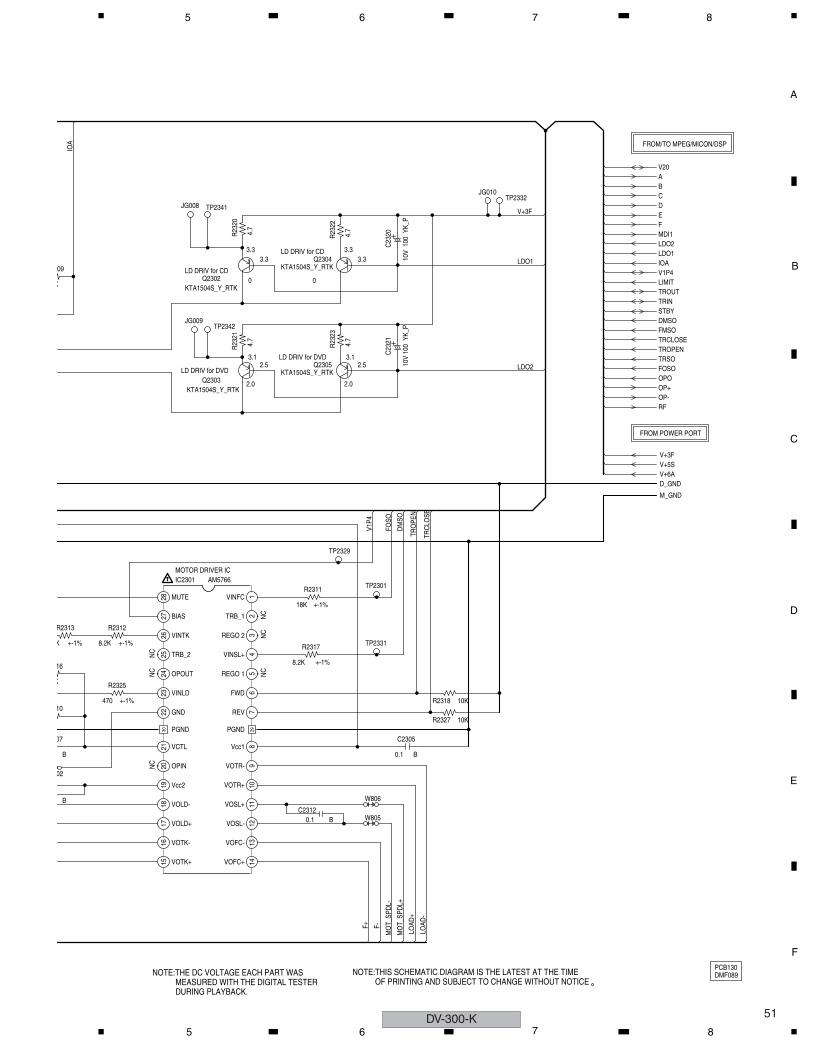
C
D
F
A
B
E
B
07
B
309
K
R2313
K +-1%
10
16
K
02
IOA
51
5 6 7 8
Q2305KTA1504S_Y_RTK
LD DRIV for DVD
Q2303KTA1504S_Y_RTK
LD DRIV for DVD
Q2304KTA1504S_Y_RTK
LD DRIV for CD
Q2302KTA1504S_Y_RTK
LD DRIV for CD
IC2301 AM5766MOTOR DRIVER IC
110
1112
131415
1617
1819
2
2021
2223
2425
2627
28
293
30
45
67
89
C23120.1 B
C2305
0.1 B
C23
21
100
10V
YK_P
C23
20
100
10V
YK_P
R23
23
4.7
R23
21
4.7
R2311
18K +-1%
R2317
8.2K +-1%
R2312
8.2K +-1%
R23
22
4.7
R23
20
4.7
R2327 10K
R2318 10K
R2325
470 +-1%
TP2342JG009
JG008TP2332
JG010
TP2341
TP2301
TP2331
TP2329
W806
W805
OF PRINTING AND SUBJECT TO CHANGE WITHOUT NOTICENOTE:THIS SCHEMATIC DIAGRAM IS THE LATEST AT THE TIME
DURING PLAYBACK.MEASURED WITH THE DIGITAL TESTER
NOTE:THE DC VOLTAGE EACH PART WAS
V20ABCD
V+3F EFMDI1LDO2LDO1IOALDO1
V1P4LIMITTROUTTRINSTBYDMSOFMSOTRCLOSETROPENTRSOFOSOLDO2
OPOOP+OP-RF
V+3FV+5SV+6AD_GND
M_GND
V1P4
FOSO
DM
SO
TRO
PEN
TRC
LOSE
MO
T_SP
DL-
MO
T_SP
DL+
F+ F-
LOAD
+
LOAD
-
0 0
3.12.5
3.1
2.0 2.0
PCB130DMF089
FROM POWER PORT
FROM/TO MPEG/MICON/DSP
3.33.3
3.33.3
2.5
Vcc1
VOTR-
VOTR+
VOSL+
VOSL-
VOFC-
VOFC+
REGO 1
VINSL+
REGO 2
TRB_1
VINFC
REV
FWD
VOTK-
VOTK+
VOLD+
VOLD-
VCTL
Vcc2
GND
VINLD
TRB_2
VINTK
BIAS
MUTE
PGNDPGND
OPOUT
OPIN
NC
NC
NC
NC
NC
NC
DV-300-K5 6 7 8
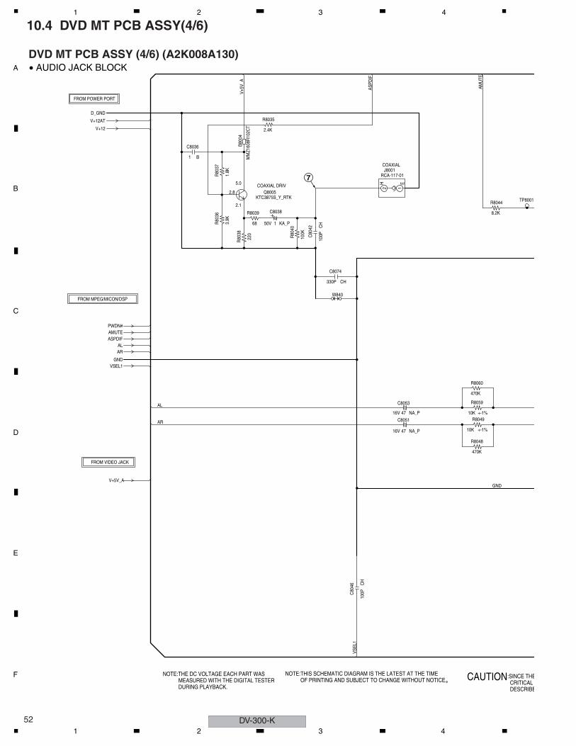
C
D
F
A
B
E
NCE THE
ESCRIBERITICAL
TP8001
DV-300-K52
1 2 3 4
10.4 DVD MT PCB ASSY(4/6)
:SICAUTIONDC
H E
J8001RCA-117-01
COAXIAL
12
C8053
4716V NA_P
C8051
4716V NA_P
Q8005KTC3875S_Y_RTK
COAXIAL DRIV
C80
42
100P
CH
C80
46
100P
CH
C8036
1 B
C8074
330P CH
C8038
150V KA_P
R80
40
100K
R8048
470K
R8060
470K
R8044
8.2K
R8059
10K +-1%R8049
10K +-1%
R80
38
220
R8035
2.4K
R80
36
3.9K
R80
37
1.8K
R8039
68
W840
OF PRINTING AND SUBJECT TO CHANGE WITHOUT NOTICENOTE:THIS SCHEMATIC DIAGRAM IS THE LATEST AT THE TIME
DURING PLAYBACK.MEASURED WITH THE DIGITAL TESTER
NOTE:THE DC VOLTAGE EACH PART WAS
B800
4
MM
Z160
8R10
2CT
ASPD
IF
AMU
TE
V+5V
_A
D_GND
V+12AT
V+12
PWDN#AMUTEASPDIF
ALAR
GNDVSEL1
AL
AR
V+5V_AGND
VSEL
1
FROM VIDEO JACK
FROM MPEG/MICON/DSP
FROM POWER PORT
2.8
2.1
5.0
DVD MT PCB ASSY (4/6) (A2K008A130)• AUDIO JACK BLOCK
7
1 2 3 4
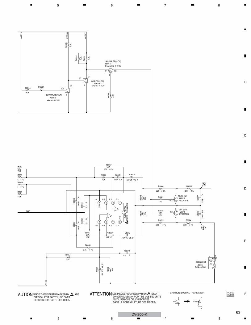
C
D
F
A
B
E
CAUTI
R8048
470K
R8060
470K
R8
8
R8059
K +-1%R8049
K +-1%
AMU
TE
G
53
5 6 7 8
:SINCE THESE PARTS MARKED BYONDESCRIBED IN PARTS LIST ONLYCRITICAL FOR SAFETY,USE ONES
ARE
DANS LA NOMENCLATURE DES PIECESN'UTILISER QUE CELLS DECRITESDANGEREUSES AN POINT DE VUE SECURITE
:LES PIECES REPAREES PAR UN ETANTATTENTION
Q8010KRC407-RTK/P
ZERO MUTE(H:ON)
Q8013KRC407-RTK/P
XAMUTE(L:ON)
H1H2
E
J8003RCA-207B-02
AUDIO OUT
1
23
CAUTION: DIGITAL TRANSISTOR
Q8018KTC2875-B
MUTE SW
Q8019KTC2875-B
MUTE SW
Q8014KTA1504S_Y_RTK
JACK MUTE(H:ON)
C8072
0.1 B
C80
58
0.1
B
C80
59
0.1
B
C80
57
560P
CH
C80
56
560P
CH
C8069
68P CH
C8067
68P CH
C80
77
330P
CH
C80
78
330P
CH
C80
66
100
10V
YK_P
C8070
4716V YK_P
C8073
4716V YK_P
R8066
10K
R8067
27K +-1%
R80
69
22K
R8085
220 +-1%
R8084
220 +-1%
R80
65
4.7K
044
.2K
R80
14
4.7K
R8061
10K
R8063
27K +-1%
R80
74
22K
R80
73
22K R8081
470
R8080
220 +-1%
R8057
22K
R8078
470
R8079
220 +-1%
R80
56
4.7K
R80
51
4.7K
TP8001
IC80
03R
C45
80ID
RAU
DIO
AM
P IC
1234
5 6 7 8
PWD
N#
V+12
AT
ND
V+12
PCB130DMF089
2.70.1
0
6.3 6.3 6.3
6.3 6.3 6.30
12.5
+-
-+
+VS
-VS
-1.2
0
0
L R
-1.20
0
0
0.30.1
0.1
0
2.7
5
6
DV-300-K5 6 7 8
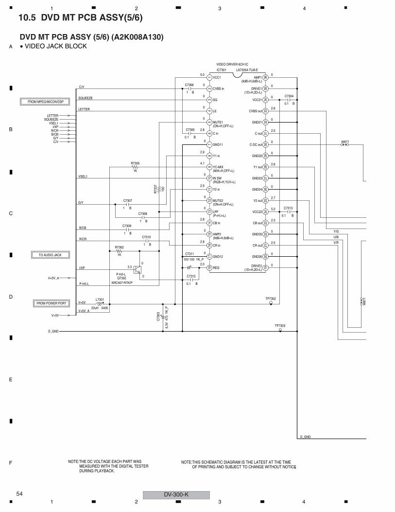
C
D
F
A
B
E
W87
1
DV-300-K54
1 2 3 4
10.5 DVD MT PCB ASSY(5/6)
IC7301 LA73054-TLM-E
VIDEO DRIVER 6CH IC
110
1112
1314
1516
1718 19
2
2021
2223
2425
2627
2829
3
3031
3233
3435
36
45
67
89
L7301
22uH 0405
Q7302KRC407-RTK/P
P-H/I-L
C7308
1 B
C7310
1 B
C7304
0.1 B
C7313
0.1 B
C7306
1 B
C7305
0.1 B
C7307
1 B
C7312
0.1 B
C7309
1 B
C73
03
470
6.3V
YK_P
C7311
10010V YK_P
R7305
1K
R73
37
100
R7302
1K
TP7303
TP7302
W877
OF PRINTING AND SUBJECT TO CHANGE WITHOUT NOTICENOTE:THIS SCHEMATIC DIAGRAM IS THE LATEST AT THE TIME
DURING PLAYBACK.MEASURED WITH THE DIGITAL TESTER
NOTE:THE DC VOLTAGE EACH PART WAS
C/V
SQUEEZE
LETTER
LETTERSQUEEZE
VSEL1I/XP
R/CRB/CB
G/YC/V
VSEL1
G/Y
B/CB
R/CR
I/XP
V+5V_A
P-H/I-L
V+5V
V+5V_AV+5V
D_GND
D_GND
TO AUDIO JACK
FROM POWER PORT
FROM MPEG/MICON/DSP
VCC1
CVBS in
SQ
LE
C in
GND11
Y1 in
Y2 in
MUTE2
CB in
AMP2
CR in
GND12
REG
GND26
CR out
GND25
CB out
VCC22
Y2 out
GND24
GND23
Y1 out
GND22
C-DC out
C out
GND21
CVBS out
VCC21
DRIVE1
AMP1
LPF
(9dB=H,6dB=L)
(P=H,I=L)
(9dB=H,6dB=L)
(ON=H,OFF=L)
DRIVE2(1D=H,2D=L)
(1D=H,2D=L)
MUTE1(ON=H,OFF=L)
IN SW(RGB=H,YUV=L)
YC-MIX(MIX=H,OFF=L)
0
0
0
0
0
0
0
0
0
0
2.6
0
0
2.5
2.6
2.7
5.0
2.5
2.5
2.8
0
2.9
4.1
2.9
0
0
0
0
2.8
0
0
2.8
2.0
0
0
5.0
3.3
0
0
Y/G
U/B
V/R
DVD MT PCB ASSY (5/6) (A2K008A130)• VIDEO JACK BLOCK
1 2 3 4

C
D
F
A
B
E
Y/G
U/B
V/R
55
5 6 7 8
H1H2
E
H1H2
E
J7302RCA-405A-08
CVBS/Y/U/V
1
23
4
56J7301
DIN-409A
S-VIDEO OUT12
34
56
CAUTION: DIGITAL TRANSISTOR
C73
24
0.1
B
C73
17 470
6.3V
YK_P
C73
19 1000
6.3V
YK_P
C73
16 470
6.3V
YK_P
C73
18 1000
6.3V
YK_P
C73
25
470
6.3V
YK_P
R73
17
75+-
1%
R73
15
75+-
1%
R73
18
75+-
1%
R73
16
75+-
1%
R73
23
75+-
1%
R73
22
75+-
1%
R73
24
10K
TP7301
W87
2
W87
3
W87
1
W877
W801
B730
5
MM
Z160
8R10
2CT
B730
4
MM
Z160
8R10
2CT
U_O
UT
V_O
UT
Y_O
UT
C YYU V CVB
S
S_C OUT
S_Y OUT
CVBS OUT
ASP
PCB130DMF089
1013 1211 8 9
DV-300-K5 6 7 8

C
D
F
A
B
E
0.00
1B
C41
00
DV-300-K56
1 2 3 4
10.6 DVD MT PCB ASSY(6/6)
CP4003A2001WV2-14P
1
10
11
12
13
14
2
3
4
5
6
7
8
9
C40
95 476.
3VKA
_P
IC4006
LM1117S-ADJ
REG+1.8V IC
123
:SINCE THESE PARTS MARKED BYCAUTIONDESCRIBED IN PARTS LIST ONLYCRITICAL FOR SAFETY,USE ONES
ARE
DANS LA NOMENCLATURE DES PIECESN'UTILISER QUE CELLS DECRITESDANGEREUSES AN POINT DE VUE SECURITE
:LES PIECES REPAREES PAR UN ETANTATTENTION
C40
99
C40
98
1B
C41
12
0.00
1B
C41
16
0.00
1B
C40
94
0.1
B
C40
86
1B
C40
93
1B
C40
96
1B
R4012
68 +-1%
R40
13
39+-
1%
R4011
15
TP4002
W820
FROM/TO POWER
(CP502)
GND
P.CON+5V
FL DC-
FL DC+
AT+3.3V
GND
P.CON+12V
AT+12V for MUTE
GND(M)
GND(D)
P.CON+6V
AT+3.3V
-28V
ADJVIN VOUT
1.8 0.63.3
P.ON-H
DVD MT PCB ASSY (6/6) (A2K008A130)• POWER PORT BLOCK
1 2 3 4

C
D
F
A
B
E
C40
98
0
57
5 6 7 8
Q4001KTC3875S_Y_RTK
ADACVDD REG
C40
99
0.00
1B
1B
C40
78
1B
C40
56
0.01
B
C41
04
0.1
B
C41
00
220
6.3V
YK_P
R40
08
1.5K +-1%
R40
21
100K
R40
35
360
+-1%
W822
W821
W826
OF PRINTING AND SUBJECT TO CHANGE WITHOUT NOTICENOTE:THIS SCHEMATIC DIAGRAM IS THE LATEST AT THE TIME
DURING PLAYBACK.MEASURED WITH THE DIGITAL TESTER
NOTE:THE DC VOLTAGE EACH PART WAS
B4001
MMZ1608R102CT
B4002
MMZ1608R102CT
V+5V
V+12AT V+12ATV+12 V+12
D_GND
V+5V
D_GND
V+6A V+6AV+5S V+5SV+3F V+3F
D_GND
M_GND
V+3 V+3V+3E V+3E
V+1R8 V+1R8
V+3A
PWDN#
FLDC-
FLDC+
-28V
D_GND
V+3
D_GND
TO LOADER/MOTOR DRIVE
TO AUDIO JACK
FROM/TO MPEG/MICON/DSP
PCB130DMF089
TO MEMORY
TO VIDEO JACK
(CORE)
(MPEG/SDRAM/FLASH)
(FIP/LED/IR/RESET)
(F/E)
(OPU)
(MOTOR)
5.0
3.9
3.3
DV-300-K5 6 7 8

C
D
F
A
B
E
12
44
111213
C67
6C
658
0.1
B47
6.3V
KA_P
P1 GR
8
GR
7
2
1
STB
0
LED1
LED2
LED4
CLK
0
K2
K1
DI
DO
OSC
LED3
PEA
P1 G8
G7
-25.
1
-25.
1
-20.
5
DV-300-K58
1 2 3 4
10.7 OPERATION 1 and OPERATION 2 PCB ASSYS
IC651PT6315
FIP DRIVER IC
13141516171819202122
2324
2526
2728
2930
3132
33
34 35 36 37 38 39 40 41 42 43
Vout
B+
GND
OS651
ROM-V340TAO
1
2
3
SW653
EVQ11L05R
ENTER
SW654
EVQ11L05R
RIGHT
SW657
EVQ11L05R
UP
SW659
EVQ11L05R
LEFT
SW661
EVQ11L05R
HOMEMENU
SW666
EVQ11L05R
EJECT
SW652
EVQ11L05R
DOWN
SW658
EVQ11L05R
TOPMENU
SW656
EVQ11L05R
MENU
SW655
EVQ11L05R
RETURN
SW66
5
EVQ
11L0
5R
PAU
SE
SW66
3
EVQ
11L0
5R
PLAY
SW66
0
EVQ
11L0
5R
STO
P
SW66
4
EVQ
11L0
5R
-SKI
P
SW66
2
EVQ
11L0
5R
+SKI
P
SW667
EVQ11L05RPOWER
V651 HNV-08SS44T
1415161718192021222324252627283132
CP6
05_1
B201
3H02
-2P
12
CP6
04_1
B201
3H02
-2P
12
D659 1SS133
D657 1SS133
D655 1SS133
D652 1SS133D651 1SS133
D654 1SS133
D656 1SS133
D658 1SS133
CD
604_
1
W9L
6020
038
C65
1
0.1
B
C67
5
C659_1
100P CH
C65
3
C67
4
476.
3VKA
_P
R666
2.2 1/4W
TP66
2
DURING PLAYBACK.MEASURED WITH THE DIGITAL TESTER
NOTE:THE DC VOLTAGE EACH PART WAS
P16
P15
P14
P13
P12
P11
P10
P9 P8 P7 P6 P5 P4 P3 P2
SW
SW
P8 P9 P10
P11
P12
P13
P14
P15
P16
P7
P6
P5
P4
P3
P2
P1
SW1
GR
8
GR
7
GR
6
GR
5
GR
4
GR
3
GR
2
GR
1
V+3E
IR
SW2
DEF129PCB280
12
VDD
23
-12.0
-6.0
-18.0
-19.0 -15.6-19.0-9.5-13.0-9.5-12.6-13.0-6.0
34VD
D
44
NC
NC
NC
NC
-18.0
-18.0
-18.0
-18.0
-18.0
-18.0
-18.0
-18.0
-16.0 -16.0 -16.0 -16.0-16.0
GND
P16
P15
P14
P13
P12
P11
P10P9P8
P7P6
GR12
P5
P4
P3
P2
P1
-28V
GR10
GR11
GR9
GR
8
GR
7
GR
6
GR
5
GR
4
GR
3
GR
2
GR
1GND
-16.0-18.0-18.0-18.0
FL+
FL+
P16
P15
P14
P13
P12
P11
P10
DVD CD TRACK ALL RE
P9 P8 P7 P6 P5 P4 P3 P2
3.3
3.3
-26.
8
-26.
8
-26.
8
-20.
5
-20.
5
-22.
7
-20.
5
-20.
5
-22.
7
-26.
8
-26.
8
-20.
5
-22.
7
-22.
7
-26.
8
-19.
7
-19.
7
SW2
POW
ER
SW2
POW
ER
SwitchesSW652 : DOWNSW653 : ENTERSW654 : RIGHTSW655 : RETURNSW656 : MENUSW657 : UPSW658 : TOPMENUSW659 : LEFTSW660 : STOPSW661 : HOMEMENUSW662 : +SKIPSW663 : PLAYSW664 : -SKIPSW665 : PAUSESW666 : EJECT
OPERATION 2 PCB ASSY(A2K001A280)
OPERATION 1 PCB ASSY(A2K008A270)
SwitchesSW667 : POWER
1 2 3 4

C
D
F
A
B
E
15
41
161718
ESTERAS
P6 P5 P4
P15
GR
2
1
19.0 -15.6
16.0 -16.0
P15
GR
2
L
P6 P5-2
6.8
-20.
5
-20.
5
59
5 6 7 8
110
11
121314
23
4
42 43 44
56
78
9
1101112131415 256789
D66
7
1SS1
33
MS1
_0
CD6012H0B1003
FFC(1.0mm pitch)
C67
6
0.1
B
C65
8
0.1
B
C67
5
0.1
B
C604
33P CHC605
0.001 B
C65
3
476.
3VKA
_P
R65
5
1K R65
7
10K
R65
6
1K R65
8
10K
R662
100K
R654
2.2
R653
2.2
R651
2.2R652
2.2
TP66
2
TP663
CP60100_6232_011_102_800+
1
10
11
2
3
4
5
6
7
8
9
W805
W80
9
OF PRINTING AND SUBJECT TO CHANGE WITHOUT NOTICENOTE:THIS SCHEMATIC DIAGRAM IS THE LATEST AT THE TIME
FLDC-
FLDC+
P3 P2 P1 GR
8
GR
7
GR
6
GR
5
GR
4
GR
3
GR
2
GR
1
SW2
-28V
SW1
P16
STB
FP_SCK
FP_DI
FP_DO
GR
1
FP_SCK
FP_DI
STB
FP_DOV+3E IR
V+3E
FLDC+
-28V
FLDC-
GND
FROM/TO MPEG/MICON/DSP
PCB270DEF126
NC
STB
2
VDD
3.2
0
0
0
LED1
LED2
LED4
CLK
VDD
44
0
0
2.9
3.2
0.7
3.4
NC
K2
K1
DI
DO
OSC
GND
P16
GR
1
GND
LED3
0
0
0
NC
NC
FL-
FL-
REPEAT A B
P4 P3 P2 P1 G8
G7
G6
G5
G4
G3
G2
G1
3.3
3.3
-25.
1
-25.
1
-25.
1
-25.
1
-25.
1
-25.
1
-25.
1
-25.
1
-20.
5
-26.
8
-26.
8
-22.
3
-22.
3
DGND
DGND
FLDC+
-28V
FLDC-
DI (M to F)
V+3E
STB
DO (F to M)
IR
CLK
(CP4002)
1
DV-300-K5 6 7 8

C
D
F
A
B
E
27
40-F
D516
1SS133
10
90-F
1
0_1
1W
R511
68 1/4W
C52
0
R51
7
1.2K
1/4W
C52
3C
521
KTC
C51
7C
522
R51
8
3.3K
+-1%
R51
6
10
OTICEIME
DV-300-K60
1 2 3 4
10.8 POWER PCB ASSY
D505
1N4005-EIC
D5
SR2
D50
9
RL1
06F-
E
D506
1N4005-EIC
D503
1N4005-EIC
D502
1N4005-EIC
D513
1H3-E
D515
1S40-E
D519
1F5-E
D5
SR2
D512_
1H3-E
D51
1
1H3-
E
D50
8
MTZ
J5.6
B
F501_11.6A125V
L501SS11V-03550-CH
COIL,LINE FILTER
1 2
3 4
FH501_1EYF-52BCY
FH502_1EYF-52BCY
IC504PS2561AL1-1-V(W)
PHOTO COUPLER
123
4
R50
2
1.5
1W
R51
2.7
REPLACE ONLY WITH THE SAME TYPE FUSE:FOR CONTINUED PROTECTION AGAINST FIRE HAZARD,CAUTION
N'UTILISER QUE DES FUSIBLE DE MEME TYPE:POUR UNE PROTECTION CONTINUE LES RISQUES D'INCEIEATTENTION
IC501 KIA431A-ATVOLTAGE CTL IC
123
CP501A3963WV2-3PDCONNECTOR
12
1.6A 125V
1.6A 125V
R507
10 1/4W
T50181291294
10
11
12
13
14
15
16
2
3
4
6
7
8 9
BLAD
EW
IDE
BLACK
WHITE
21
CD5010Q618902
AC120V_60Hz(US)
C51
1
8240
0VU
P_P
:SINCE THESE PARTS MARKED BYCAUTIONDESCRIBED IN PARTS LIST ONLYCRITICAL FOR SAFETY,USE ONES
ARE
DANS LA NOMENCLATURE DES PIECESN'UTILISER QUE CELLS DECRITESDANGEREUSES AN POINT DE VUE SECURITE
:LES PIECES REPAREES PAR UN ETANTATTENTION
C503
0.1 B
C51
3
47P
2KV
SL
C51
6
0.00
2225
0VKX
C51
8
0.00
125
0VKX
C50
2_1
0.22
275V
ECQ
UL
C51
5_1
0.01
400V
ECQ
P
C50
8
680P
CH
C540
0.0068 B
C50
9
1050
VYK
_P
C50
6
2.2
50V
KA_P
R50
3
1.5M
1/2W
R505
22 1/4W
R515
1K
R514
1K 1/4W
R50
4
680K
R51
2_1
100K
1/2W
R513
6.8K 1/4W
IC50
2ST
R-A
6131
MPO
WER
CTL
IC
1 2 3 4
5678
OF PRINTING AND SUBJECT TO CHANGE WITHOUT NNOTE:THIS SCHEMATIC DIAGRAM IS THE LATEST AT THE T
B501
W4B
RH
3.5X
6X1.
0X2
1.6A 125VF501_1
1.6A 125VF501_1
NTSC
L
N
NC
NC
0
0
0
0
0
0
0
130
130
0
130
0
-22.5
-22.5
NCDD
OC
P
VCC
GN
D
FB/O
LPST
ARTU
P
17.5 3.90.1
130 130 130
0
0 NC
0 2.59.9
GNDOUT IN
9.90
3.9 10.9
CHASSIS GND
POWER PCB ASSY (A2K008A240)
PRIMARY side
* The parts except mark cannot be changed. On that occasion, replace whole Assy.
1 2 3 4

C
D
F
A
B
E
D5
1S4
D
1
501 KIA431OLTAGE CTL
23
C540
0.0068
515
K
3
/4W
HANGE WITLATEST A
0 2
GNDUT
61
5 6 7 8
IS NON POLAR ONE.THE ALUMI ELECTROLYTIC CAPACITOR MARKED NPTHE RESISTOR MARKED F IS FUSE RESISTOR.NOTE:
D52
1
1SS1
33
D52
0
1SS1
33
D52
2
1SS1
33D534
1SS133
D532
1S40-E
D527
SR240-F
D52
5
1SS1
33
D516
1SS133
15
0-E
519
F5-E
D510
SR290-F
D512_1
1H3-E
D533
MTZJ2.2B
D53
6
MTZ
J3.0
B
D51
7
MTZ
J2.2
B
D52
3
MTZ
J3.6
B
D53
5
MTZ
J5.1
B
D53
1
MTZ
J27B
D52
8
MTZ
J5.1
B
R529
220 1W
R510_1
2.7 1W
A-AT IC
1
R511
68 1/4W
Q506KTA1504S_Y_RTK
PROTECT
IC503PQ070XF01SZH
+6V REG (DVD MOTOR) IC
1 2 3 4
C52
0
100
50V
YK_P
CD502CU2E3301
CORD CONNECTOR
R51
7
1.2K
1/4W
+-1%
R546
3.3K 1/4W+-1%
CD6003TD-OR0201R
TM60107650KY060
BT601
R6P(AR)XICI
UM-4
CP502A2001WV2-14P
1
10
11
12
13
14
2
3
4
5
6
7
8
9
C52
3
470
25V
YK_P
C52
1
1000
16V
ZL_P
C53
6
220
6.3V
YK_P
C52
6
470
6.3V
YK_P
C53
1
100
16V
YK_P
C53
5 330
16V YK
_P
L505
22uH
L503
22uH TSL0808
Q505KRC102SRTK
P.CON SW
CAUTION: DIGITAL TRANSISTOR
Q509KTC3875S_Y_RTK
REG+12V CTL
Q501KTC3875S_Y_RTK
PROTECT
Q511KTC3875S_Y_RTK
REG+12V CTL
Q512 KTC3875S_Y_RTKFL+ CTL
Q502 KTC3209_Y-28V P.CON SW
Q515 2SD1835S/T-AAP.CON+5V REG
Q510 KTA1281_YP.CON+12V SW
Q504KTA1281_Y
FL+ P.CON SW
Q513KTA1504S_Y_RTK
FL+ CTL
Q503KTA1504S_Y_RTK-28V CTL
C503
0.1 B
C50
1
0.01
B
C541
0.01 B
B
C51
7
220
25V
YK_P
C52
8 2.2
50V KA
_P
C53
8
220
6.3V
YK_P
C52
7 100
10V YK
_P
C52
2 1000
6.3V ZL
_P
C51
9 2235
V YK_P
R53
8
22K
R50
9
1K
R534
100 1/4W
R52
6
6.8K
+-1%
R51
8
3.3K
+-1%
R52
3
22K
R51
9
3.3K
R52
4
1K1/
4W
R545
22K +-1%
R525
100
R547
22
R54
1
5.6K
+-1%
R54
2
470
+-1%
R54
3
4.7K
+-1%
R53
9
4.7K
1/4W
R527
100 1/4W
R50
6
100
R51
6
10
R514
1K 1/4W
R54
0
680
R53
0
560
1/4W
R53
6
10K
R54
4
10K
R548
1K
R528
22K 1/4W
R53
1
10K
R537
1K
W817
W81
4
HOUT NOTICET THE TIME
DURING PLAYBACK.MEASURED WITH THE DIGITAL TESTER
NOTE:THE DC VOLTAGE EACH PART WAS
B502
W5RH3.5X5X1.0
(W023)
GND
FROM/TO POWER PORT
PCB240DPF015
1.207.0 5.9
0
02.8
4.5
5.012.3
(CP4003)
ACCESSORY
0
9.9
0
3.2
0
3.2
P.CON+12V
P.CON+5V
FL DC-
FL DC+
GND
GND
AT+12V for MUTE
P.CON+6V
-28V
GND(M)
GND(D)
AT+3.3V
AT+3.3V
P.ON-H(STBY L)
.5
IN
4.5
12.95.1
12.6
12.3
12.9
19.0
0.6
0
20.8
28.4
28.4
27.8
5.8
5.17.0
6.80.6
0
21.521.6
19.719.0
20.7
IN GNDOUT ADJ
DV-300-K5 6 7 8
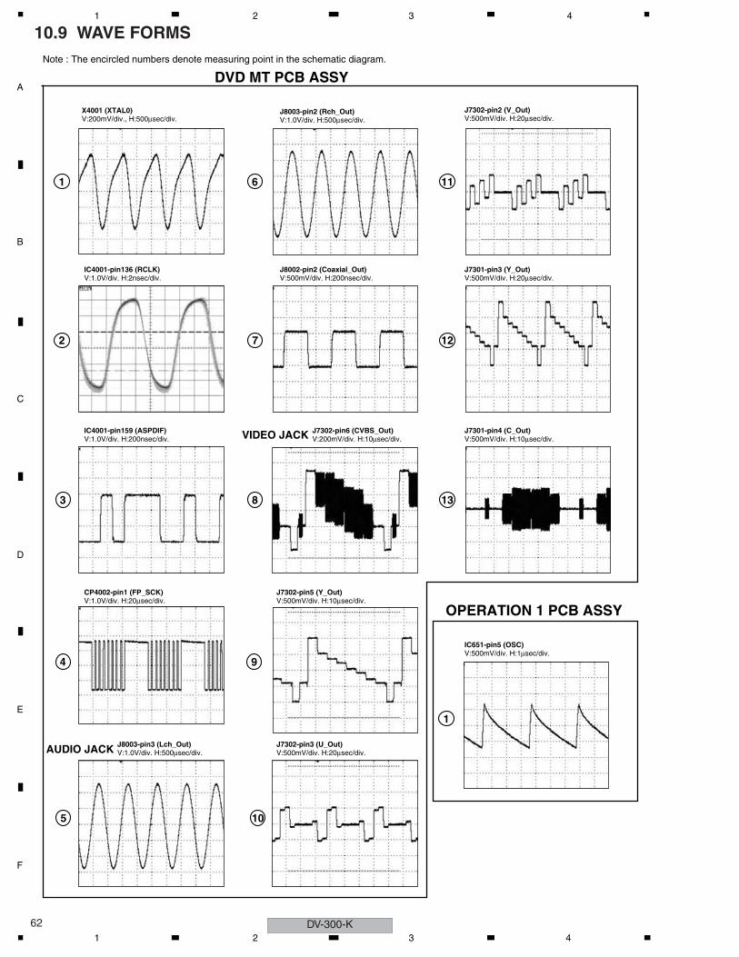
C
D
F
A
B
E
DV-300-K62
1 2 3 4
10.9 WAVE FORMS
1
1
X4001 (XTAL0)V:200mV/div., H:500µsec/div.
IC4001-pin136 (RCLK)V:1.0V/div. H:2nsec/div.
IC4001-pin159 (ASPDIF)V:1.0V/div. H:200nsec/div.
CP4002-pin1 (FP_SCK)V:1.0V/div. H:20µsec/div.
J8003-pin3 (Lch_Out)V:1.0V/div. H:500µsec/div.
2
3
4
5
6
7
8
9
10
11
12
13
DVD MT PCB ASSY
OPERATION 1 PCB ASSY
Note : The encircled numbers denote measuring point in the schematic diagram.
J8003-pin2 (Rch_Out)V:1.0V/div. H:500µsec/div.
J8002-pin2 (Coaxial_Out)V:500mV/div. H:200nsec/div.
J7301-pin3 (Y_Out)V:500mV/div. H:20µsec/div.
J7302-pin6 (CVBS_Out)V:200mV/div. H:10µsec/div.
J7301-pin4 (C_Out)V:500mV/div. H:10µsec/div.
J7302-pin5 (Y_Out)V:500mV/div. H:10µsec/div.
J7302-pin3 (U_Out)V:500mV/div. H:20µsec/div.
J7302-pin2 (V_Out)V:500mV/div. H:20µsec/div.
IC651-pin5 (OSC)V:500mV/div. H:1µsec/div.
AUDIO JACK
VIDEO JACK
1 2 3 4
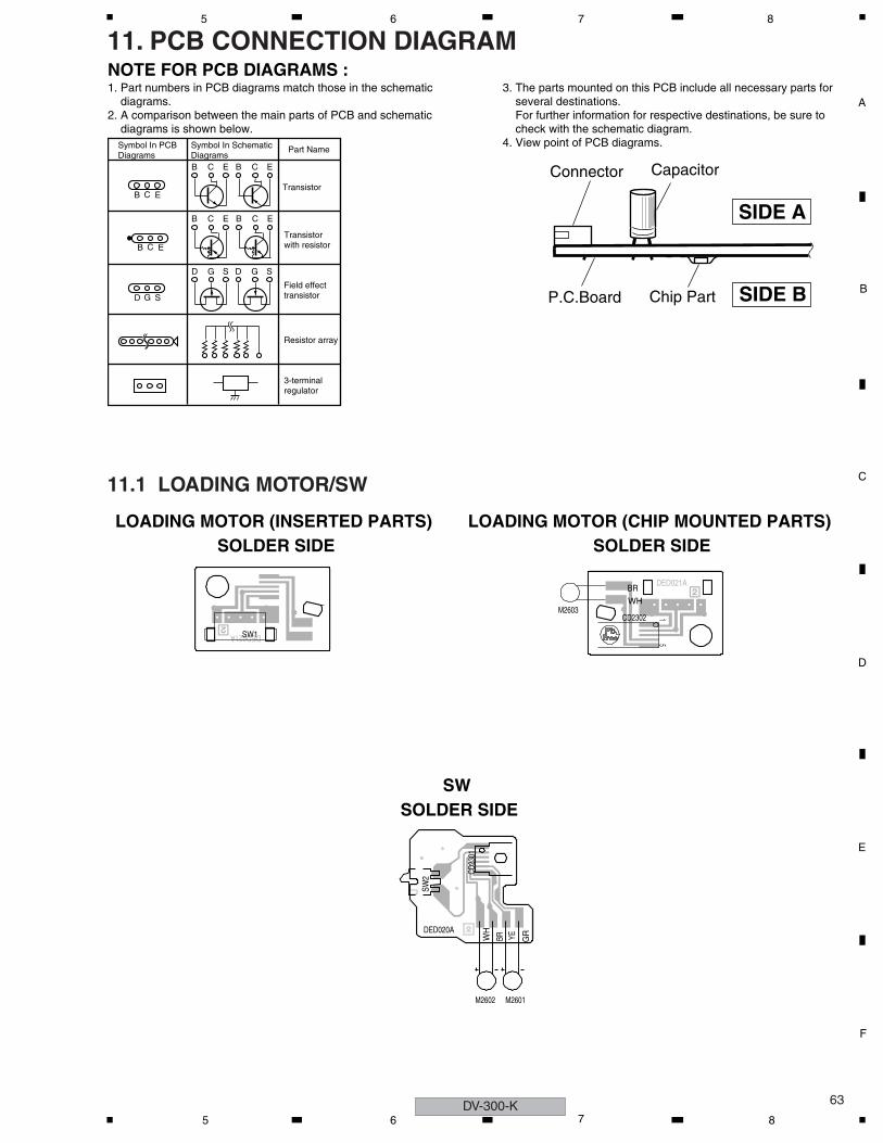
C
D
F
A
B
E
63
5 6 7 8
11. PCB CONNECTION DIAGRAM
11.1 LOADING MOTOR/SW
NOTE FOR PCB DIAGRAMS :1. Part numbers in PCB diagrams match those in the schematic diagrams.2. A comparison between the main parts of PCB and schematic diagrams is shown below.
3. The parts mounted on this PCB include all necessary parts for several destinations. For further information for respective destinations, be sure to check with the schematic diagram.4. View point of PCB diagrams.Symbol In PCB
DiagramsSymbol In SchematicDiagrams
Part Name
B C E
D
D
G
G
S
S
B C E
B C E
D G S
B C E B C E
B C E
Transistor
Transistorwith resistor
Field effecttransistor
Resistor array
3-terminalregulator
CapacitorConnector
P.C.Board Chip Part
SIDE A
SIDE B
DED021A
DED021A
M2601M2602
CD23
01
SW2
GRYEWH
BR
DED020A
BR
WH
51
M2603CD2302
SOLDER SIDESW
SOLDER SIDELOADING MOTOR (CHIP MOUNTED PARTS)
SOLDER SIDELOADING MOTOR (INSERTED PARTS)
SW1
DV-300-K5 6 7 8

C
D
F
A
B
E
DV-300-K64
1 2 3 4
11.2 DVD MT PCB ASSY
DMF089A
163 109
551
DVD MT PCB ASSY
SIDE ASIDE A
W83
9
C231
2
R7337
B400
7
C2317_1
W871
R732
3
W873
W87
2
C7324
C732
5
R732
2
W87
7
R7324
W80
1
J730
1
W82
0
Q2307Q2306
R2316
Q40
01
L7301
C803
8
W80
5
W806
C230
7
C231
1R2
310
W802
R231
3R2
312
R230
4
R232
7
R231
8
R231
7
R2311
IC40
02R4
076
CP4003
R7305
C7310
C7309
C230
6
IC2301
Q8013Q8018
B4011
R401
1
C805
3
C805
1
Q80
10
C730
3
CP4002
R4035
J800
3
C411
6
IC8003
C4112
C408
0
C7308C7307
C7306
C7305
C731
1
C405
2
R405
7
C406
7C4
066
R4046R4045
R4052
R4051
R4050
R4049
C4059C4
039
C404
7
C4081
R400
4R4
002
R403
9R4
037
IC73
01
IC4006
IC4005
IC4004
IC40
03
R7317
R730
2
R406
6
R4040
R403
6
Q73
02
C8036
C410
0
C4099
C4098
C4096
C409
5
C4094
C407
1
B8004
B4002
B400
1
R401
3
B7305
B730
4
R7318
R731
6
R7315
C731
9C7
318
C731
7
C731
6
J800
1
R406
5
R407
5
R4029
R4025
R401
5
C807
8C8
077
C807
2
C8069
C8067
C805
9C8
058
C805
7
C805
6
C8046
C804
2
C4077
C404
8
C4049
C406
2
C408
8
C407
9
C4073
C403
6C4
035
C4031C4034
C402
9
C4027 C402
5C4
024
C402
2C4
020
C401
9
C4018
C401
6
C400
6
C401
4C4
013
C401
2
C401
1
C408
9
C409
0
C2301
CP2301
IC4001
NR4002
NR40
01
W840
CP2303
CP2302
C807
0C8
073
C806
6
C232
1
C232
0
R803
6
R803
5
R803
8R8
040 R8
039
R8084
R8037
R8085
R8079
R8080
R807
8
R808
1R8
074
R807
3
R805
6
R806
7
R8063 R8048R8049
R806
1R8
066
R806
9
R8057
R4022
R4020
R402
4
R401
2
R230
9
R401
8 R4014
R4009
R230
6
R400
6
R230
7
R400
7R2
323
R232
1 R232
0
R2322
R4010
R407
4R4
034
R233
8
R233
1
R2319R2329
Q80
05
Q23
03
Q2304Q8019
Q80
14 Q2301
Q23
05
Q2302
J730
2
X400
1C4
030
C405
0
1 2 3 4
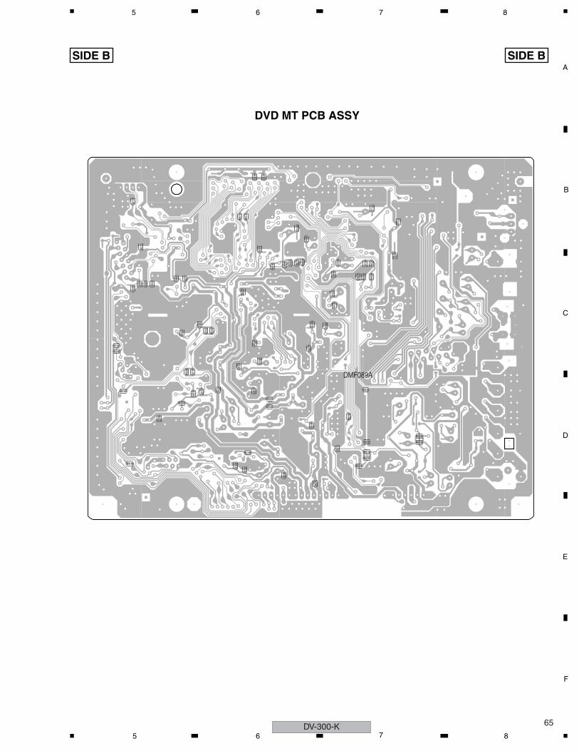
C
D
F
A
B
E
65
5 6 7 8
DMF089A
DVD MT PCB ASSY
SIDE B SIDE B
W82
6
W814
C230
5
R2325
C410
2
R806
5
R8044
R8051
R8014
C411
8
B401
0
R400
8
C407
8
C410
4
R402
1
C402
8
C403
2
C407
4
W834
W833
R407
3
R407
2
C404
0
C400
1
R8060
R8059
C730
4C7
313
C731
2
C405
5
R2341
R2343
R4001
C410
1
C407
2
R405
8
C405
8
C406
5
C406
4
C406
3
C403
8C4
046
C403
7C4
033
C402
6
C408
2 C408
3
C408
4C4
114
C406
0
C232
3
C232
2
R234
2
R400
3
C410
3
C405
7C4
023
C807
4
C409
3C4
056
R2308
C408
6
C230
3
C230
2
W821
W822
C400
7
C400
5R4
061
C400
3
C400
2
C405
1
DV-300-K5 6 7 8

C
D
F
A
B
E
DV-300-K66
1 2 3 4
11.3 OPERATION 1 PCB and OPERATION 2 PCB ASSYS
DEF1
29A
DEF1
26A
DEF1
29A
DEF1
26A
12
1
34
23
12
1
34
23
OPERATION 1 PCB ASSY (INSERTED PARTS)
OPERATION 1 PCB ASSY (CHIP MOUNTED PARTS)
OPERATION 2 PCB ASSY(CHIP MOUNTED PARTS)
OPERATION 2 PCB ASSY(INSERTED PARTS)
SIDE A SIDE A
W809
W80
5
R666
CP60
5_1
SW66
7
OS6
51
D658
D657
D656
D655
W01
7
CP60
4_1
W01
6W
015
W013
W011
D659
D652
D654
W010
W012
SW66
4SW
662
SW66
0SW
665
SW66
3
D651
W009W007
W00
4
W003
CP60
1
C674
W00
1
C653
D667
V651
SW66
6
SW66
1
SW65
8
SW659
SW65
2
SW65
3
SW65
7
SW65
4SW
655
SW65
6
C659_1
C604
C605
C651
C676
C658
C675
R662
R658R657
R656R655
R654
R653R652
R651
IC651
1 2 3 4
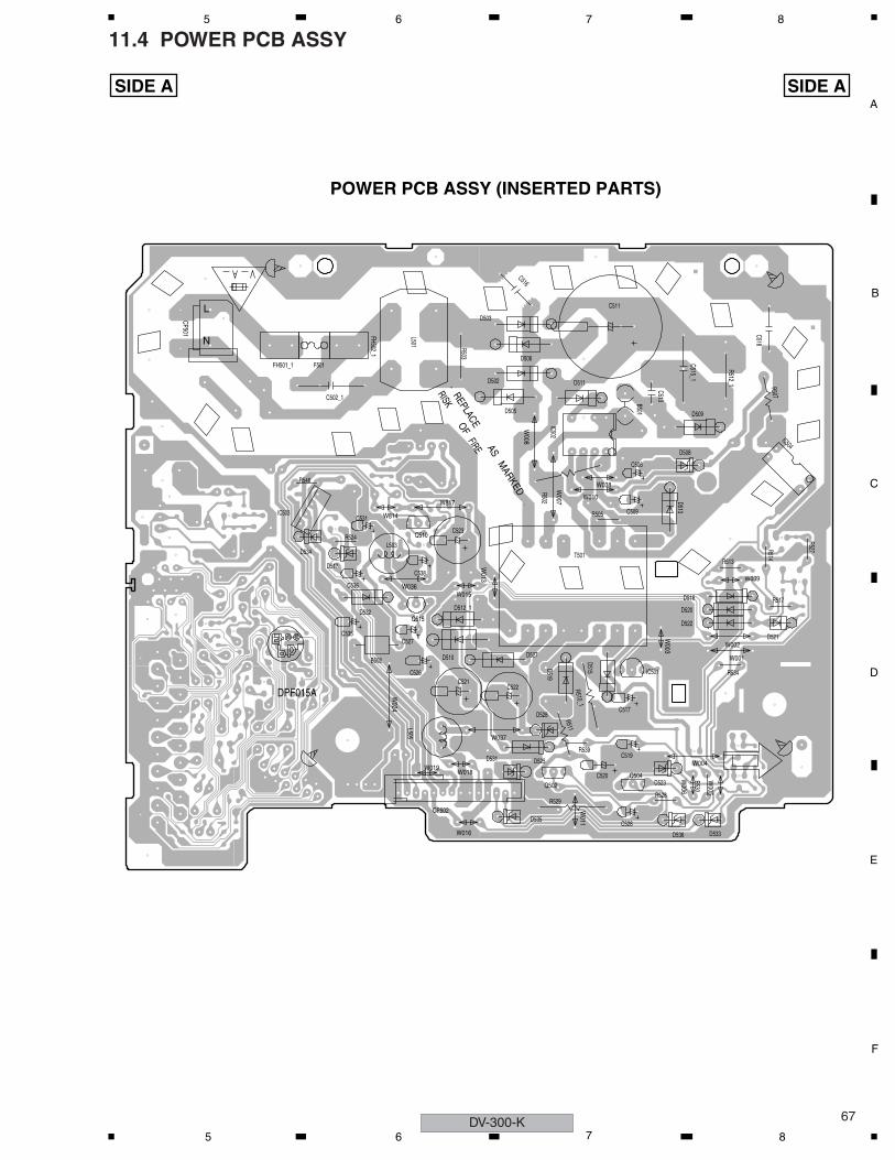
C
D
F
A
B
E
67
5 6 7 8
11.4 POWER PCB ASSY
DPF015A
.
MARKED
AS
REPLACE
-
FIRE
OF
RISK
POWER PCB ASSY (INSERTED PARTS)
SIDE A SIDE A
W817
W039
D512_1
D510B502
W024
Q515
Q502
D527
R512_1
R503
W011
W038
W010
W007
W008
W002
W004
W001
W036
CP502
W037
C526
C528
D536
C527
C521
D535
C515_1
C522
D517
R524
C516
R510_1
C513
C518
R546
D534
W814
D532
C523
W015
D525
C520
R539
D515
IC503
D533
C506
Q510
D519
D513
D511
W013
R502
W019W018
C535
R527
R505C531
T501
D531
W016
R528R529
W005
C536
L503
L505
C538
Q504
R534
R530
W006
D523
C519
R517
D521
D528
D516
D520
D522
R511
W003
R514
R513
C517
IC501
IC504
R507
D508
C509
IC502
C511
L501
D509
B501D505
D502
D506
D503CP501
F501FH501_1
FH502_1
C502_1
L
N
DV-300-K5 6 7 8
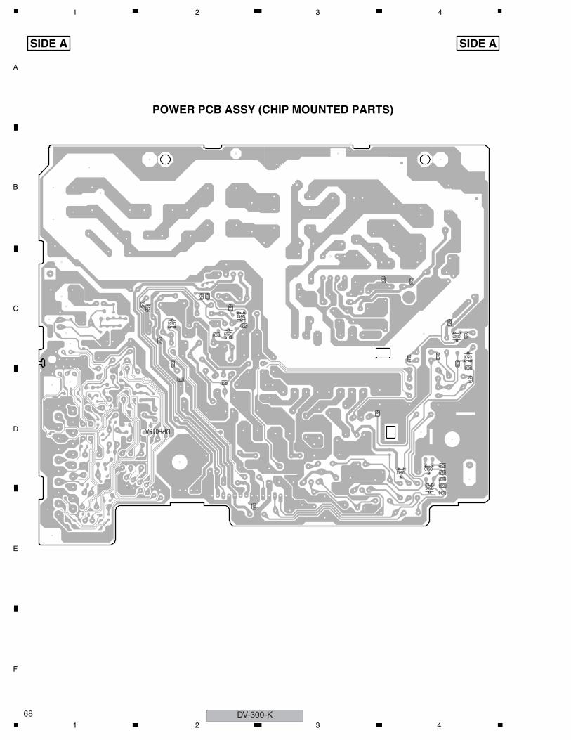
C
D
F
A
B
E
DV-300-K68
1 2 3 4
DPF015A
POWER PCB ASSY (CHIP MOUNTED PARTS)
SIDE A SIDE A
C540
R542
R540
R548
R525
R547R519
R526R545
C501
C541
R531
R536R537
R544Q513
Q505
R509
R543
R541
Q509
Q511
Q503
Q512
R506 R538
Q506
R523Q501
R516
R518
C503
R515
R504
C508
1 2 3 4
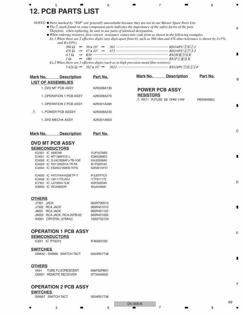
C
D
F
A
B
E
69
5 6 7 8
12. PCB PARTS LIST Parts marked by "NSP" are generally unavailable because they are not in our Master Spare Parts List.The mark found on some component parts indicates the importance of the safety factor of the part.Therefore, when replacing, be sure to use parts of identical designation.When ordering resistors, first convert resistance values into code form as shown in the following examples.Ex.1 When there are 2 effective digits (any digit apart from 0), such as 560 ohm and 47k ohm (tolerance is shown by J=5%, and K=10%).
Ex.2 When there are 3 effective digits (such as in high precision metal film resistors).
5 6 14 7 3
R 5 01 R 0
5 6 2 1
NOTES:
560 Ω47k Ω0.5 Ω1 Ω
RD1/4PU JRD1/4PU JRN2H KRS1P K
56 x 10 1
47 x 10 3
R501R0
561473
5.62k Ω RN1/4PC F562 x 10 1 5621
Mark No. Description Part No.LIST OF ASSEMBLIES 1..DVD MT PCB ASSY A2K008A130 1..OPERATION 1 PCB ASSY A2K008A270 1..OPERATION 2 PCB ASSY A2K001A280 > 1..POWER PCB ASSSY A2K008A240 1..DVD MECHA ASSY A2K001A650
Mark No. Description Part No.
DVD MT PCB ASSYSEMICONDUCTORS
IC2301 IC AM5766 I1UFV5766SIC4001 IC MT1389FE/E-L IC8K0389E0IC4002 IC S-24CS08AFJ-TB-1GE I5HJ0S08A0IC4003 IC R3112N291A-TR-FA IE1F0291A0IC4004 IC ES29LV160EB-70TG S2K001AF01
IC4005 IC HY57V641620ETP-7 IF3J0TP7C0IC4006 IC LM1117S-ADJ I1TF911170IC7301 IC LA73054-TLM I03FG30540IC8003 IC RC4580IDR I04J045800
OTHERSJ7301 JACK 063R700013J7302 RCA JACK 060R451010J8001 RCA JACK 060R401122J8003 RCA JACK, RCA-207B-02 060R451009X4001 CRYSTAL (27MHz) 100GT02720
OPERATION 1 PCB ASSYSEMICONDUCTORS
IC651 IC PT6315 IF4K063150
SWITCHES SW652 - SW666 SWITCH TACT 0504R01T38
OTHERSV651 TUBE FLUORESCENT 096F82R601OS651 REMOTE RECEIVER 077A040002
OPERATION 2 PCB ASSYSWITCHES
SW667 SWITCH TACT 0504R01T38
POWER PCB ASSYRESISTORS
> R511 R,FUSE 68 OHM 1/4W R65584680J
Mark No. Description Part No.
DV-300-K5 6 7 8