tohoku university graduate school of engineeringeprints.utem.edu.my/14955/1/micro electrical...
TRANSCRIPT

TOHOKU UNIVERSITY
Graduate School of Engineering
Micro Electrical Discharge Machining of Reaction-bonded
Silicon Carbide
A dissertation submitted for the degree of Doctor of Philosophy (Engineering)
Department of Mechanical Systems and Design
by
LIEW Pay Jun
July 12, 2013
Micro Electrical Discharge Machining of Reaction-bonded Silicon Carbide
LIEW Pay Jun
Abstract
Functional micro-structures are gaining more and more importance in the industrial technologies during the last few years. For example, deep micro holes find a wide range of applications in inkjet printer nozzles, spinnerets holes, turbine blades cooling channels, diesel fuel injection nozzles, drug delivery orifices, etc. Another important example is microlens arrays. The ability of microlens arrays to focus incident light into a series of beam spots makes them useful as important optical elements that are widely used in the area of optoelectronic and optical communications. Due to the wide applications of these functional micro-structures in optical, biomedical engineering and microelectromechanical systems (MEMS), micro fabrication techniques have gained growing interest from researchers and engineers.
Recently, the use of reaction-bonded silicon carbide (RB-SiC) as a material in manufacturing optical molding dies for aspherical lenses and microlens arrays has become a new research focus, due to its superior material properties, such as high hardness and strength at elevated temperature, high thermal conductivity, chemical stability, wear resistance and low density. However, due to its high hardness (Vickers hardness 25-35 GPa), it is typically difficult to be machined. Although abrasive machining processes, such as lapping, polishing and grinding can produce a fine surface finish, but the machining efficiency is low and the production cost is high. Diamond cutting is able to produce a high material removal rate, but the severe tool wear in diamond cutting of RB-SiC is the main obstacle that limits its wide application in the industry. Compared to the aforementioned methods, micro electrical discharge machining (micro-EDM) has emerged as a possibly effective machining tool to fabricate complex micro-structures on hard and difficult-to-cut materials like RB-SiC. However, the use of conventional micro-EDM alone to obtain micro-structures with good surface finish and high form accuracy in RB-SiC, is still a challenging issue. The high resistivity of the RB-SiC workpiece is the main limiting factor for the discharge current of micro-EDM, which directly affects the machining efficiency of RB-SiC.
The main objective of this study is to develop hybrid machining processes based on micro-EDM for improving the machinability and surface finish of RB-SiC. Carbon nanofibers assisted micro-EDM was proposed to replace the conventional micro-EDM. The effects of carbon nanofibers addition in the dielectric fluid were confirmed experimentally. The machining mechanism and the material migration phenomenon with the addition of carbon nanofibers were investigated and clarified. Next, a novel machining process, namely hybrid micro-EDM process by combining ultrasonic cavitation and carbon nanofibers was proposed, in order to improve the machining efficiency of RB-SiC ceramic material and to prevent from tool material deposition on workpiece. The effectiveness of the hybrid process was verified through the fabrication of micro-structures on RB-SiC.
This thesis consists of five chapters. Chapter 1 gives an overview of the background of this research. Firstly, an introduction of the RB-SiC ceramic material, including the fabrication process, material properties, applications and previous machining processes of RB-SiC material were given. EDM was chosen as a method to fabricate micro-structures on the RB-SiC, which can overcome the shortcomings of the abrasive machining process. Then, an overview of the principle of micro-EDM/EDM process was discussed. The problem of machining RB-SiC by using conventional EDM was also pointed out. Some recent developments for enhancing the machinability of hard and brittle ceramic materials by micro-EDM/EDM were reviewed. Finally the objectives and organization of this thesis were stated.
Micro-EDM is primarily an electro-thermal machining process for conductive material. However, the RB-SiC that was used in this study possesses very low conductivity, which made the machining process unstable. This problem becomes more pronounced during the fabrication of micro deep holes and other micro-structures such as micro dimples and micro grooves. Therefore, in Chapter 2, carbon nanofiber assisted micro-EDM was proposed. In this process, carbon nanofibers measuring 150 nm in diameter and 6-8 µm in length were added
I
into the dielectric fluid. Unlike the conventional EDM, carbon nanofibers can arrange themselves in the form of micro chains and interlock to each other, which help to form bridging networks between the electrode and the workpiece. Furthermore, the excellent electrical conductivity of carbon nanofiber (10-4 [km) also reduces the insulating strength of the dielectric fluid. To verify the proposed method, firstly, simulation of electric field distribution and direction of the electric force were conducted with a commercial finite element analysis (FEA) software package, COMSOL Multiphysics. It is expected that under the influence of electric force, carbon nanofibers will be concentrated around both electrodes, and will align themselves in the form of chain in the direction of flow of current. The effect of carbon nanofiber on gap width was then studied analytically and verified through preliminary experiments. The experimental results were in good agreement with the analytical study, where carbon nanofibers were more effective in increasing the spark gap and material removal rate of RB-SiC compared to spherical carbon powders. Next, the changes in electro discharging behavior, material removal rate, electrode wear ratio, electrode geometry, spark gap, surface finish, surface topography and surface damage with carbon nanofiber concentration were examined experimentally. It was found that the addition of carbon nanofiber not only improved the electro discharge frequency, material removal rate, discharge gap and surface finish, but also reduced the electrode wear and electrode tip concavity. Micropores and microcracks were found on the machined surface, and the mechanism of micropores formation was different from that in micro EDM of conductive metals. Bidirectional material migrations between the electrode and the workpiece surface were also detected, and the migration behavior was strongly suppressed by carbon nanofiber addition. Adhesion of carbon nanofibers to the workpiece surface occurred, which contributed to the improvement of electro discharge machinability.
Material migration between electrode and workpiece is difficult to be avoided during EDM processes. Especially when performing EDM in the micro/nano scale, the effect of material migration may play an important role from the viewpoint of mechanical and physical properties of the machined surface. In order to clarify its fundamental mechanism, in Chapter 3, material migration between tool electrode and workpiece material in micro-EDM of RB-SiC was experimentally investigated. The microstructural changes of workpiece and tungsten tool electrode were examined using scanning electron microscopy (SEM), cross-sectional transmission electron microscopy (TEM) and energy dispersive X-ray spectroscopy (EDX) under various voltage, capacitance and carbon nanofiber concentration in the dielectric fluid. The RB-SiC that was used in this research, consists of crystalline 6H-SiC grains and crystalline bonding silicon. During the EDM process, the Si matrix, in conjunction with sintering agents, possesses a higher electrical conductivity than the 6H-SiC grains, so it was preferentially removed by melting and vaporization, leaving craters on the surface. The melted tungsten electrode particles were deposited intensively inside the discharge-induced craters on the RB-SiC surface as amorphous structure forming micro particles, and on flat surface region as a thin interdiffusion layer of poly-crystalline structure. The formation mechanism of the subsurface layer in this work was distinctly different from those in mechanical machining processes such as diamond turning, which mainly phase-transformed from the bulk material by mechanical stresses. Deposition of carbon element on tool electrode was also detected, indicating possible material migration to the tool electrode from workpiece material, carbon nanofibers and dielectric oil. Material deposition rate was strongly affected by workpiece surface roughness, voltage and capacitance of the electrical discharge circuit. For reducing the migration and deposition of tool material, the capacitance should be kept as low as possible and the voltage at moderately high level. Adding carbon nanofibers into the dielectric fluid at a concentration of 0.06 g/L was helpful. These findings are useful for improving the surface integrity and purity ofRB-SiC in micro-EDM.
In micro-EDM, due to the narrow sparking gap, the removal of debris is remaining a challenging issue, especially in deep holes machining and fine finishing with lower discharge energy. The deposition of tool material on the workpiece surface not only caused surface contamination, but also deteriorated the surface finish of the workpiece. Conventionally, orbital electrode actuation, flushing, planetary movement of electrode, ultrasonic vibration, etc were used to overcome these problems. In Chapter 4, in order to suppress the tool material deposition and improve the machining efficiency ofRB-SiC ceramic material, a new machining method, namely hybrid EDM process by combining ultrasonic cavitation and carbon nanofibers was proposed. In this method, suitable amount of carbon nanofibers were added and mixed uniformly in the dielectric fluid. An oscillator horn was placed into the compound dielectric fluid and ultrasonic vibration was used to generate cavitation to assist micro electrical discharge machining. For comparison, another two types of micro-EDM tests were then carried out, namely, carbon nanofibers addition in EDM oil only, and ultrasonic cavitation in pure EDM oil. Changes of hole depth, hole geometry, surface topography, machining stability and tool material deposition rate under various machining conditions were investigated experimentally. The results show that the ultrasonic vibration-induced cloud cavitation was very helpful for increasing sparking gap and removing debris, especially when carbon nano fibers were added into the dielectric fluid. The combination of ultrasonic cavitation and carbon nanofibers can improve the maximum hole depth, form accuracy, and surface finish of micro holes to a significant degree. The tool material deposition rate was strongly affected by the ultrasonic vibration amplitude
II
and the distance between the oscillator and workpiece during fine finishing. The main mechanism for removing the debris from the sparking gap was through the oscillation of the cloud cavitation, rather than the collapse of micro bubbles. The cloud cavitation tends to oscillate at the working area due to the pressure fluctuation in dielectric fluid which was induced by low intensity ultrasonic waves. In a cloud cavitation, the nonlinear bubble dynamics produced nonlinear interactive effects which caused cascading of fluctuation energy. This fluctuating energy was helpful to flush out the debris from the working gap. As test pieces, aspect ratio of 21. 7 micro deep hole was successfully fabricated on RB-SiC at a high machining speed. Under fine finishing conditions, micro dimples with good cross-sectional profile and minimum tungsten deposition were successfully obtained. The proposed hybrid EDM process has been demonstrated to be helpful for fabricating micro-structures on hard brittle ceramic materials.
In Chapter 5, the general conclusions of this research were summarized.
As a summary, in this dissertation, carbon nanofibers assisted micro-EDM has been developed to enhance the machinability of low conductivity RB-SiC ceramic materials. Material migration phenomena during the micro-EDM process were clarified. The optimal conditions to control the material migration in micro-EDM of ceramic materials and to improve the finished surface topography and surface integrity were confirmed. By using the proposed hybrid EDM process with combination of ultrasonic cavitation and addition of carbon nanofibers in dielectric fluid, tool material deposition was significantly suppressed and machining efficiency was improved 5-7 times compared to the one obtained with merely ultrasonic cavitation or carbon nanofibers addition. With this method, high aspect ratio micro holes and good cross-sectional profile micro dimples with minimum tungsten deposition were successfully fabricated on hard and brittle RB-SiC ceramic material. By applying the new process proposed in this dissertation, the production cycle and cost involved may significantly reduce compared to the conventional process.
TABLE OF CONTENTS
Chapter 1 Introduction···························································· 1
1.1 Reaction-bonded silicon carbide (RB-SiC) · · · · · · · · · · · · · · · · · · · · · · · · · · · · · · · · · · · · · · · · · · · · · 1
1.1.1 Fabrication process ofRB-SiC························································ 2
1.1.2 Material properties and microstructure · · · · · · · · · · · · · · · · · · · · · · · · · · · · · · · · · · · · · · · · · · · · · · 3
1.1.3 Applications of RB-SiC · · · · · · · · · · · · · · · · · · · · · · · · · · · · · · · · · · · · · · · · · · · · · · · · · · · · · · · · · · · · · · · · 5
1.1.4 Machining processes for RB-SiC · · · · · · · · · · · · · · · · · · · · · · · · · · · · · · · · · · · · · · · · · · · · · · · · · · · · · 6
1.2 Overview of electrical discharge machining (EDM) · · · · · · · · · · · · · · · · · · · · · · · · · · · · · · · · · · 7
1.2.1 Principle ofEDM ······ ··············· ··············· ························· ·········· 8
1.2.2 Micro-EDM and its types····························································· 11
1.3 Micro-EDM of hard and brittle ceramic material····································· 14
1.3.1 Powders mixed EDM (PMEDM)···················································· 15
1.3.2 Assisting electrode EDM ··························· ········ ················· ········ · 17
1.3.3 Electrical discharge milling and mechanical grinding···························· 18
1.4 Objectives and organization of the dissertation .. ····················· .. ·············· 19
1.5 References·················································································· 20
Chapter 2 Carbon Nanofiber Assisted Micro-EDM · ·· ······· ............. · 25
2.1 Carbon nanofibers assisted micro-EDM mechanism································· 25
2.1.1 Orientation principle of carbon nanofibers · · · · · · · · · · · · · · · · · · · · · · · · · · · · · · · · · · · · · · · · · 27
2.2 Analytical study of the mechanism of CNFs assisted micro-EDM ·· ········ ····· · 27
2.2.1 Force acting on carbon nanofiber in an electric field····························· 27
2.2.2 Effect of carbon nanofiber in gap width············································ 30
2.2.3 Preliminary experimental verification · · · · · · · · · · · · · · · · · · · · · · · · · · · · · · · · · · · · · · · · · · · · · · 32
2.3 Experimental methods···································································· 35
I
2.3.1 Machine tool············································································ 35
2.3.2 Carbon nanofibers · · · · · · · · · · · · · · · · · · · · · · · · · · · · · · · · · · · · · · · · · · · · · · · · · · · · · · · · · · · ·· · · · · · · · · 36
2.3.3 Electrode · · · · · · · · · · · · · · · · · · · · · · · · · · · · · · · · · · · · · · · · · · · · · · · · · · · · · · · · · · · · · · · · · · · · · · · · · · · · · · · · 38
2.3.4 Machining conditions · · · · · · · · · · · · · · · · · · · · · · · · · ·· · · · · · · · · · · · · · · · · · · · · · · · · · · · · · · · · · · · · · · 39
2.3 .5 Measurement and evaluation························································· 41
2 .4 Experimental results and discussion··· · · · · · · · · · · · · · · · · · · · · · · · · · · · · · · · · · · · · · · · · · · · · · · · · · 41
2.4.1 Electro discharge behavior · · · · · · · · · · · · · · · · · · · · · · · · · · · · · · · · · · · · · · · · · · · · · · · · · · · · · · · · · · · 41
2.4.2 Material removal rate·································································· 43
2.4.3 Electrode wear ratio · · · · · · · · · · · · · · · · · · · · · · · · · · · · · · · · · · · · · · · · · · · · · · · · · · · · · · · · · · · · · · · · · · · 45
2.4.4 Spark gap················································································ 48
2.4.5 Surface roughness······································································ 49
2.4.6 Surface topography···································································· 50
2.4.7 Material migration phenomena······················································ 55
2.5 Chapter summary ............................................................... ··· ...... ·· 60
2.6 References·················································································· 61
Chapter 3 Material Migration Phenomena in Micro-EDM··············· 63
3 .1 Experimental methods · · · · · · · · · · · · · · · · · · · · · · · · · · · · · · · · · · · · · · · · · · · · · · · · · · · · · · · · · · · · · · · · · · · · 64
3.1.1 EDM conditions········································································ 64
3 .2 Results and discussion········ · · · · · · · · · · · · · · · · · · · · · · · · · · · · · · · · · · · · · · · · · · · · · · · · · · · · · · · · · · · · 66
3.2.1 Material deposition phenomena······················································ 66
3.2.2 Effect of voltage········································································ 69
3.2.3 Effect of capacitance · · · · · · · · · · · · · · · · · · · · · · · · · · · · · · · · · · · · · · · · · · · · · · · · · · · · · · · · · · · · · · · · · · 72
3.2.4 Effect of carbon nanofiber concentration···················· .. ············ .. ······· 76
3 .2.5 Cross-sectional TEM observation · · · · · · · · · · · · · · · · · · · · · · · · · · · · · · · · · · · · .... · · · · · · · · · .. 77
3.3 Material migration mechanism·························································· 83
3 .4 Chapter summary·························· · · · · · · · · · · · · · · · · · · · · · · · · · · · · · · · · · · · · · · · · · · · · · · · · 85
II
3.5 References·················································································· 85
Chapter 4 Ultrasonic Cavitation Assisted Micro-EDM ·· ·············· ···· 88
4.1 Cavitation assisted micro-EDM with addition of carbon nanofibers · · · · · · · · · · · · · · 89
4.2 Experimental method · · · · · · · · · · · · · · · · · · · · · · · · · · · · · · · · · · · · · · · · · · · · · · · · · · · · · · · · · · · · · · · · · · · · · 90
4.2.1 Equipment··············································································· 90
4.2.2 Machining conditions · · · · · · · · · · · · · · · · · · · · · · · · · · · · · · · · · · · · · · · · · · · · · · · · · · · · · · · · · · · · · · · · · 92
4.3 Results and discussion···································································· 93
4.3.1 Rough machining······································································ 93
4.3 .1.1 Effect of vibration amplitude · · · · · · · · · · · · · · · · · · · · · · · · · · · · · · · · · · · · · · · · · · · · · · · · · · · · · 93
4.3.1.2 Hybrid effect of ultrasonic cavitation and carbon nanofiber addition······· 96
4.3 .1.3 Micro hole geometry······························································· 97
4.3.1.4 Surface topography······························································· 100
4.3.1.5 Stabilityofmachiningprocess·················································· 103
4.3.2 Fine finishing········································································· 105
4.3 .2.1 Effect of vibration amplitude on tungsten deposition · · · · · · · · · · · · · · · · · · · · · · · 105
4.3.2.2 Effect of working distance on tungsten deposition·························· 107
4.4 Process mechanism······································································ 108
4.5 Applications·············································································· 111
4.5.1 Fabrication of high aspect ratio micro hole · · · · · · · · · · · · · · · · · · · · · · · · · · · · · · · · · · · · · · 111
4.5.1.1 Cross-section of high aspect ratio micro hole · · · · · · · · · · · · · · · · · · · · · · · · · · · · · · · · 113
4.5.2 Fabrication of micro dimple array on RB-SiC·· · · · · · · · · · ·· · · · · · · · · · · · · · · · · · · · · · · 115
4. 6 Chapter summary· · · · · · · · · · · · · · · · · · · · · · · · · · · · · · · · · · · · · · · · · · · · · · · · · · · · · · · · · · · · · · · · · · · · · · · · 118
4.7 References················································································ 119
Chapter 5 General Conclusions · · · · · · · · · · · · · · · · · · · · · · · · · · · · · · · · · · · · · · · · · · · · · · 121
List of Publications································· Error! Bookmark not defined.
Acknowledgements································································ 125
III
Chapter 1 Introduction
In recent years, the use of ceramics materials such as silicon carbide (SiC), alumina and
silicon nitride has received intensive attention in mechanical and manufacturing engineering.
The advantages of ceramics over other materials include high hardness and strength at
elevated temperature, chemical stability, wear resistance and low density (Agarwal and Rao,
2008).
Reaction-bonded silicon carbide (RB-SiC), one of the most prom1smg ceramics
materials, are widely used as molding dies for manufacturing ultraprecision glass lenses
owing to its excellent properties. Increasing the machining rate while maintaining the desired
surface integrity is the major concern in the machining of RB-SiC. However, due to its high
hardness, RB-SiC is extremely difficult to be machined. Although abrasive machining
processes, such as lapping, polishing and grinding can produce a fine surface finish, but the
material removal rate is low. Diamond cutting of RB-SiC has been proved to be able to
produce a high material removal rate, but severe tool wear still remains to be a problem in its
industrial applications. In particular, the fabrication of micro-structures and high aspect ratio
micro shapes on hard and brittle ceramics by using abrasive machining, usually difficult and
involve high production cost. Therefore, it has become the main obstacle to the widespread
use of ceramics materials in industries nowadays.
For these reasons, this dissertation focuses on developing new technologies for
machining RB-SiC by using micro electrical discharge machining (micro-EDM), since it
proved to be an effective method for machining hard and brittle ceramic materials,
particularly for applications where complex micro geometries with dimensional accuracy are
primary requirement.
1.1 Reaction-bonded silicon carbide (RB-SiC)
Silicon carbide is one of the most important materials of the group of non-oxide
ceramics. It is well suited for wide applications in harsh environments, due to its good thermal
1
Micro Electrical Discharge Machining of Reaction-bonded Silicon Carbide
conductivity, high radiation resistance and high breakdown voltage (Choyke et al., 2004).
Recently, the use of SiC as molding dies for manufacturing aspherical glass lenses is getting
popular (Hall et al., 2005), owing to its superior characteristics. Among the ceramics
materials, RB-SiC is considered as one of the most promising materials of the SiC ceramics
family. The fabrication process for RB-SiC is slightly different from the conventional
methods for the SiC. From the viewpoints of dense structure, low processing temperature,
good shape capability, low cost and high purity, reaction sintering is considered as one of the
new processes for SiC (Suyama et al., 2003). The detail fabrication process will be explained
in the next section.
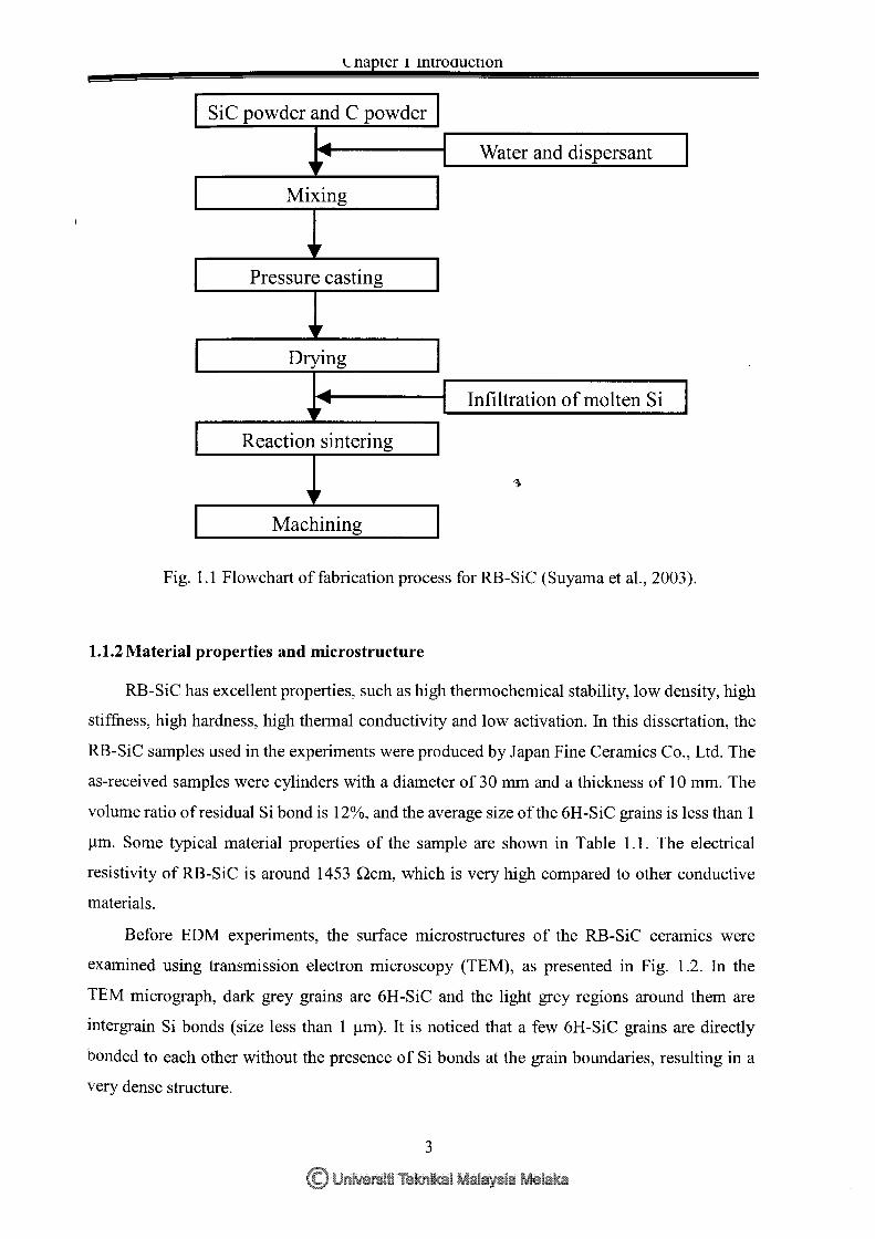
1.1.1 Fabrication process of RB-SiC
Conventionally, manufacturing processes for SiC are pressureless sintering, gas pressure
sintering, hot pressing, hot isostatic pressing, chemical vapor deposition, re-crystallization and
reaction sintering. As for RB-SiC, it is fabricated by infiltrating melted silicon (Si) into a
green body consisting of carbon (C) and SiC (mostly 6H-SiC) powders. The flowchart of
fabrication process for RB-SiC is shown in Fig. 1.1. Firstly, the raw material which composes
of certain ratio of SiC powders and C powders, are mixed with water and some dispersant.
The original preform, also called as green body, is formed by pressure casting of the slurry.
The green body is dried and then reaction-sintered at 1693 K in vacuum for 1 hour. At the
same time, melted Si is infiltrated into the green body. At this high temperature, the molten Si
reacts with the C particles, forming new SiC particles. However, the infiltrated molten Si
cannot react with C completely, therefore, excess Si remains in the body as a bonding
material. In this way, a very dense Si-SiC composite with excessive silicon is produced
(Suyama et al., 2003).
Lnapter 1 mtroaucnon
SiC powder and C powder
Water and dispersant
Mixing
Pressure casting
Drying
Infiltration of molten Si
Reaction sintering
Machining
Fig. 1.1 Flowchart of fabrication process for RB-SiC (Suyama et al., 2003).
1.1.2 Material properties and microstructure
RB-SiC has excellent properties, such as high thermochemical stability, low density, high
stiffness, high hardness, high thermal conductivity and low activation. In this dissertation, the
RB-SiC samples used in the experiments were produced by Japan Fine Ceramics Co., Ltd. The
as-received samples were cylinders with a diameter of 30 mm and a thickness of 10 mm. The
volume ratio ofresidual Si bond is 12%, and the average size of the 6H-SiC grains is less than 1
µm. Some typical material properties of the sample are shown in Table 1.1. The electrical
resistivity of RB-SiC is around 1453 Qcm, which is very high compared to other conductive
materials.
Before EDM experiments, the surface microstructures of the RB-SiC ceramics were
examined using transmission electron microscopy (TEM), as presented in Fig. 1.2. In the
TEM micrograph, dark grey grains are 6H-SiC and the light grey regions around them are
intergrain Si bonds (size less than 1 µm). It is noticed that a few 6H-SiC grains are directly
bonded to each other without the presence of Si bonds at the grain boundaries, resulting in a
very dense structure.
3

Micro Electrical Discharge Machining of Reaction-bonded Silicon Carbide
Table 1.1 Material properties of RB-SiC.
Properties Values
Si/SiC volume ratio(%/%) 12/88
Density p (g/cm3) 3.12
Young modulus E (GPa) 407
Softening temperature (°C ) 1375
Electrical resistivity (Qcm) ~1453
Vickers hardness (GPa) 25-35
Bending strength RT (MP a) 780
Thermal expansion coefficient (1 o-6 /K) 3.23
Thermal conductivity (W /m · K) 143
Porosity (%) <0.1
Fig. 1.2 Microstructures ofRB-SiC observed by TEM.

Chapter 1 Introduction
1.1.3 Applications of RB-SiC
RB-SiC has a wide variety of industrial applications. Nowadays, RB-SiC has been
thought to be a prospective material for the large-scale light-weight mirrors which used in the
precision optical system. Besides that, it is also widely used as molding dies for
manufacturing ultraprecision glass lenses in optical manufacturing industry. Due to its
excellent thermo-mechanical characteristics such as high thermal stability and conductivity,
RB-SiC also has been used extensively as heat exchanger parts for hydrogen production
systems. Other applications of this material are shown in Fig. 1.3 .
• • RB-SiC • •
Fig. 1.3 Applications of RB-SiC (Adapted from Suyama and Itoh, 2006).
5

Micro Electrical Discharge Machining of Reaction-bonded Silicon Carbide
1.1.4 Machining processes for RB-SiC
To obtain a good surface finish and high dimensional accuracy on hard and brittle
RB-SiC ceramic material are remained a challenging issue. Due to its high hardness (Vickers
hardness 25-35 GPa), RB-SiC is extremely difficult to be machined. Many efforts have been
made by previous researchers on abrasive machining of RB-SiC. For example, Tam et al.
(2007) investigated the lapping and polishing of RB-SiC using various kinds of abrasives. The
fabrication process of RB-SiC optical components was divided into two stages. At first, for
rapid removal of surface error and initial smoothing, a plate fixed with solid pellet-shaped
diamond abrasives was used. Subsequently, felt buffs and diamond abrasives were used to
perform fine error removal and surface polishing.
Besides lapping and polishing, grinding process also has been widely used to machine
hard and brittle material. For instance, Dai et al. (2005) used electrolytic in-process dressing
(ELID) to grind the high strength RB-SiC. For comparison, cup type and straight type metal
bond diamond wheels were used for the grinding test. Generally speaking, eventhough these
abrasive machining processes could produce a very fine surface finish, but the material
removal rate is low and the production cycle is long, which normally include many separate
operations. Furthermore, it is rather difficult to generate micro-structures such as micro-lens
array, micro pyramids on the RB-SiC molding dies with abrasive machining processes.
Single point diamond turning (SPDT) is another important machining method to
fabricate micro-structures on hard and brittle material such as single crystal silicon, glass and
ceramic. Diamond cutting of RB-SiC was recently attempted by Yan et al. (2009). Although
diamond cutting could produce a high material removal rate, however, severe tool wear still
remains to be a problem, which limits its application in industrial.
Recently, electrical discharge machining (EDM) has become popular to machine hard
ceramics material. The growing popularity of EDM can be attributed to its advantages, such
as low installation cost and its ability to machine complex three-dimensional shapes easily
regardless of material hardness (Reynaerts et al., 1998). Furthermore, during machining with
micro-EDM, there is no direct contact between the electrode and workpiece, thus eliminating
mechanical stress, chatter and vibration problems (Ho and Newman, 2003). EDM has been
used extensively for machining various ceramic materials. For example, a comparative study
of the die-sinking EDM of three different ceramic materials was carried out by Puertas and
Luis (2004). Clijsters et al. (2010) also manufactured complex parts on SiSiC materials using
EDM. However, most ceramics are not sufficiently conductive, which is a major problem
Chapter 1 Introduction
when applying EDM to ceramics materials. Konig et al. (1988) indicated that 100 Ocm is the
upper limit of electrical resistivity for a ceramic workpiece to be machined by EDM. As pure
SiC has a far higher electrical resistivity ( ~ 105 ncm), it is impossible to be machined directly
by EDM. For RB-SiC, due to the presence of free Si (normally poly-crystalline) and other
small-amount additives in the SiC bulk, the electrical conductivity can be improved to some
extent (Wilhelm et al., 1999). The conductivity of RB-SiC, however, is still very poor if
compared to other conductive materials. Hence, the EDM machining efficiency of RB-SiC is
extremely low and the EDM process is unstable. For these reasons, this dissertation will focus
on developing new technologies for improving the EDM machinability of low conductivity
RB-SiC mold material.
1.2 Overview of electrical discharge machining (EDM)
Electrical discharge machining (EDM), also known as spark machining, 1s an
electro-thermal machining process, whereby a desired shape is obtained using electrical
discharges (sparks). In EDM, both electrode and workpiece are submerged in a dielectric fluid,
which is generally kerosene or deionized water. During the process, there is no mechanical
contact between the electrode and the workpiece. The electrical sparks are generated in a
dielectric fluid by electrical energy, and act as a cutting tool, to remove the workpiece
material by melting and evaporation. The volume removed by a single spark is small, in the
range of 10-6-10-4 mm3, however the sparks occur at a high frequency, typically 10000 times
per second (Descoeudres, 2006).
The dielectric fluid plays an important role in the EDM process. According to
Kalpakjian and Schmid (2001), the dielectric fluid acts as an insulator and flushing medium to
carry away the debris and provide the cooling medium to the tool and the workpiece. The
machining performance of EDM is depends on many factors, such as electrode material,
workpiece material, non-electrical machining parameters, and electrical machining parameters.
Fig. 1.4 shows the Ishikawa cause-effect diagram for EDM process.
7

Micro Electrical Discharge Machining of Reaction-bonded Silicon Carbide
Material Semi-conductive
Size
Supply voltage Capacitance Flushing
Peak current Feed rate
Pulse on time Working time
Non-conductive
Conductive
Electrical discharge machining
Dielectric fluid type
Rotation of electrode
Fig. 1.4 Ishikawa cause-effect diagram of EDM process.
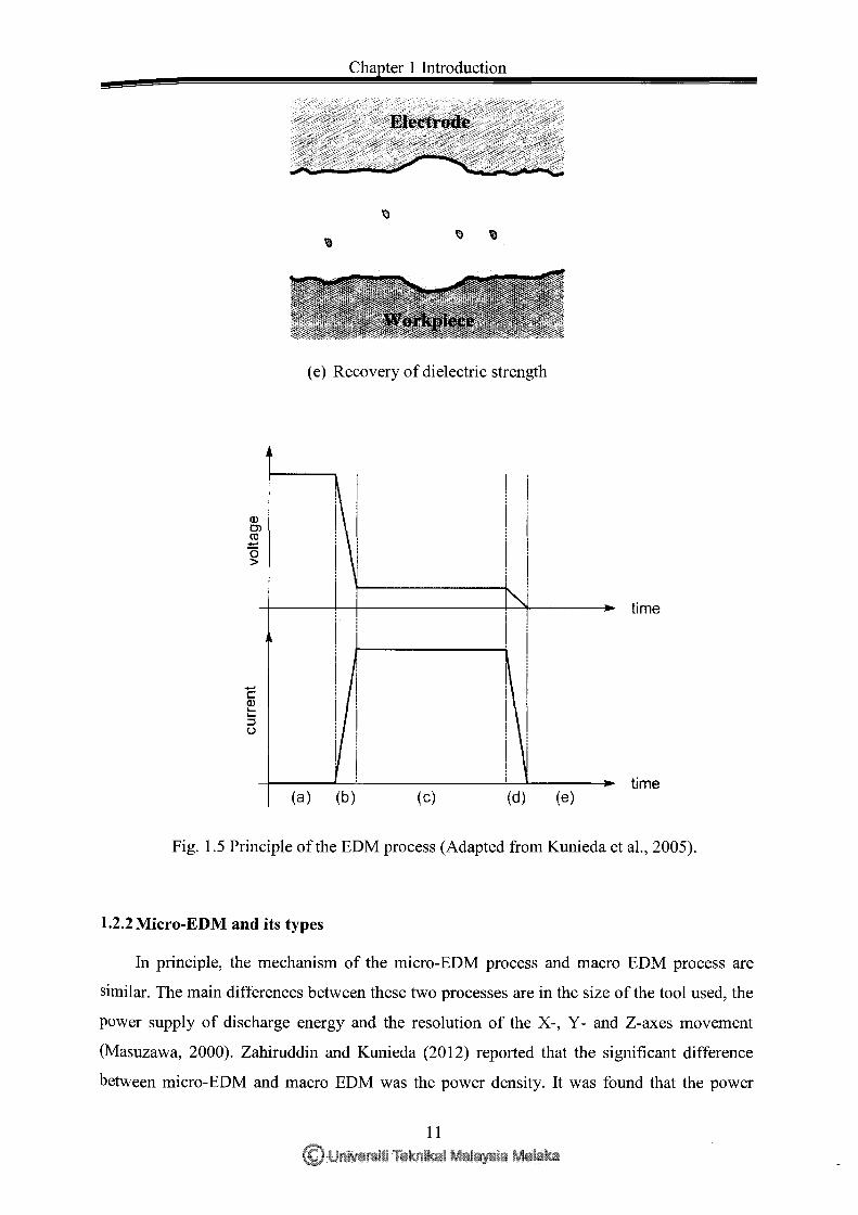
1.2.1 Principle of EDM
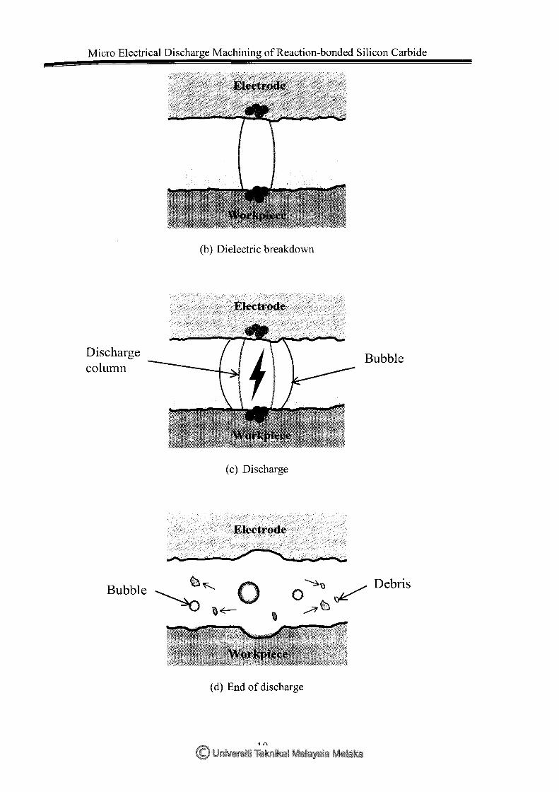
According to Schumacher (2004), the sparking phenomena or electrical discharge during
EDM can be separated into three important phases, namely preparation phase for ignition,
phase of discharge and interval phase between discharges. Fig. 1.5 gives an overview of the
erosion process due to a single EDM discharge. The phenomena of sparking are briefly
explained, as below:
(a) Voltage is applied between the electrode and the workpiece. At low electric current,
electrons passing through the dielectric fluid from the negative electrode towards the
positive workpiece, and vice versa. An electric field or energy column is created.
(b) At the closest point between the electrode and workpiece, the breakdown of the dielectric
fluid is initiated. When the breakdown occurs, the voltage falls and a current rises
abruptly. A plasma channel (ionized, electrically conductive gas with high temperature) is
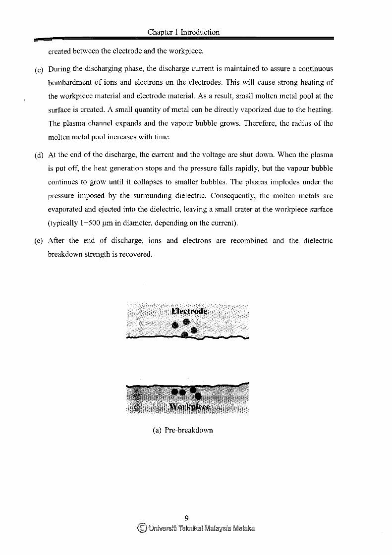
Chapter 1 Introduction
created between the electrode and the workpiece.
( c) During the discharging phase, the discharge current is maintained to assure a continuous
bombardment of ions and electrons on the electrodes. This will cause strong heating of
the workpiece material and electrode material. As a result, small molten metal pool at the
surface is created. A small quantity of metal can be directly vaporized due to the heating.
The plasma channel expands and the vapour bubble grows. Therefore, the radius of the
molten metal pool increases with time.
( d) At the end of the discharge, the current and the voltage are shut down. When the plasma
is put off, the heat generation stops and the pressure falls rapidly, but the vapour bubble
continues to grow until it collapses to smaller bubbles. The plasma implodes under the
pressure imposed by the surrounding dielectric. Consequently, the molten metals are
evaporated and ejected into the dielectric, leaving a small crater at the workpiece surface
(typically 1-500 µmin diameter, depending on the current).
( e) After the end of discharge, ions and electrons are recombined and the dielectric
breakdown strength is recovered.
(a) Pre-breakdown
9
Micro Electrical Discharge Machining of Reaction-bonded Silicon Carbide
Discharge column
Bubble
(b) Dielectric breakdown
( c) Discharge
Bubble
O ~\l / Debris
~~
( d) End of discharge
Q) rn ro ...... 0 >
Chapter 1 Introduction
( e) Recovery of dielectric strength
(a) (b ( c) (d)
time
time (e)
Fig. 1.5 Principle of the EDM process (Adapted from Kunieda et al., 2005).
1.2.2 Micro-EDM and its types
In principle, the mechanism of the micro-EDM process and macro EDM process are
similar. The main differences between these two processes are in the size of the tool used, the
power supply of discharge energy and the resolution of the X-, Y- and Z-axes movement
(Masuzawa, 2000). Zahiruddin and Kunieda (2012) reported that the significant difference
between micro-EDM and macro EDM was the power density. It was found that the power
11

Micro Electrical Discharge Machining of Reaction-bonded Silicon Carbide
density of micro-EDM was approximately 30 times greater than that of macro EDM.
Consequently, energy efficiency and removal efficiency in micro-EDM were significantly
greater than those of macro EDM.
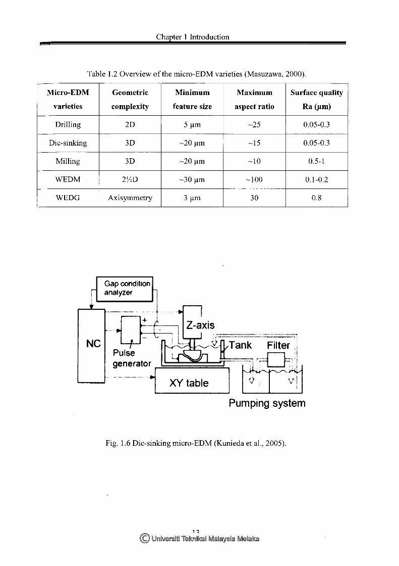
There are four different types of micro-EDM technologies which used for manufacturing
micro-features, namely die-sinking micro-EDM (an electrode with micro-features is employed
to produce its mirror image in the workpiece), micro-wire EDM (a wire is used to cut through a
conductive workpiece), micro-EDM drilling (micro-electrodes are used to 'drill' micro-holes in
the workpiece), and micro-EDM milling (micro-electrodes are employed to produce
three-dimensional cavities by adopting a movement strategy similar to that in conventional
milling) (Pham et al., 2004). Table 1.2 shows an overview of the capabilities of micro-EDM
(Masuzawa, 2000).
In the micro-EDM machine that was used in this dissertation, two mam types of
machining can be distinguished, namely die-sinking micro-EDM and wire electro-discharge
grinding (WEDO). In die-sinking EDM (Fig. 1.6), the workpiece is formed either by
replication of the shaped tool electrode, or by three-dimensional movement of a simple
electrode. Normally, negative electrode polarity is used when performing test using die
sinking EDM. Tungsten rod, which shaped by WEDO is normally used as an electrode, and
fed in the z-direction, towards the workpiece that immersed in the dielectric fluid. WEDO,
which was developed by Masuzawa et al. (1985), uses a brass wire to erode away material
from a rotating workpiece to produce a cylindrical shaft (Fig. 1. 7). The workpiece (anode) is
held vertically in a mandrel that rotates at 3000 rpm, and its position is slowly fed in the
z-direction. A ¢100 µm brass wire (cathode) is supported on a wire guide, and its position is
controlled in the x- and y-directions. The electrical discharges which produced by
resistor-capacitor (RC) erode material from the workpiece and the brass wire, within a small
gap (~ 2µm) filled with dielectric oil (Morgan, 2004). Die-sinking EDM is mainly used to
produce injection molds, whereas the wire-cutting EDM is widely used in the production of
steel cutting dies and extrusion dies (Descoeudres, 2006).
Chapter 1 Introduction
Table 1.2 Overview of the micro-EDM varieties (Masuzawa, 2000).
Micro-EDM
varieties
Drilling
Die-sinking
Milling
WEDM
WEDG
Geometric
complexity
2D
3D
3D
2ViD
Axisymmetry
Gap condition analyzer
' !------•
Minimum
feature size
5µm
-20 µm
-20 µm
-30 µm
3µm
NC Pulse generator ,.......!::======-_____ ------1 XY table
Maximum Surface quality
aspect ratio Ra (µm)
-25 0.05-0.3
-15 0.05-0.3
-10 0.5-1
-100 0.1-0.2
30 0.8
vi
Pumping system
Fig. 1.6 Die-sinking micro-EDM (Kunieda et al., 2005).

Micro Electrical Discharge Machining of Reaction-bonded Silicon Carbide
Fig. 1.7 Wire electro-discharge grinding (WEDG) (Morgan, 2004).
1.3 Micro-EDM of hard and brittle ceramic material
When machining hard and brittle ceramic materials by EDM, information about the
workpiece conductivity/resistivity is therefore an absolute prior requirement. The resistivity
of the workpiece is a limiting factor for the discharge current, which directly affects the
material removal rate (Lee et al., 2013). Various materials with their resistivity are shown in
Fig. 1.8. As mentioned earlier, 100 Ocm is the upper limit of electrical resistivity for a
ceramic workpiece to be machined by EDM (Konig et al., 1988). However, most ceramics are
not sufficiently conductive, which is a major problem when applying EDM to ceramics
materials. For example, the RB-SiC ceramic material that was used in this study, possesses a
very high electrical resistivity, which is around 1453 ncm. It is typically difficult to be
machined directly by EDM. Hence, the method for increasing the EDM machinability of
materials is crucial. From the past researches, there are several methods have been used, as
summarized in the following sub-sections.

---- Spark erosion
Silver
Copper
Aluminium
Iron
Chapter 1 Introduction
RB-SiC (1453)
SiC
Glass
10-6 m-s m-4 m-3 m-2 m-1 mo 101 102 103 m4 ms m6 m1 ms m9 m10 mu m12 m13 mt4
r M"W t-- Sem;co,ducto' ---+1•1+-• --- Som; ;,.u\atm ------r-- hrnulatm --1
Fig_ 1.8 Resistivity of various materials (Ocm) (Adapted from Lee et al., 2013).
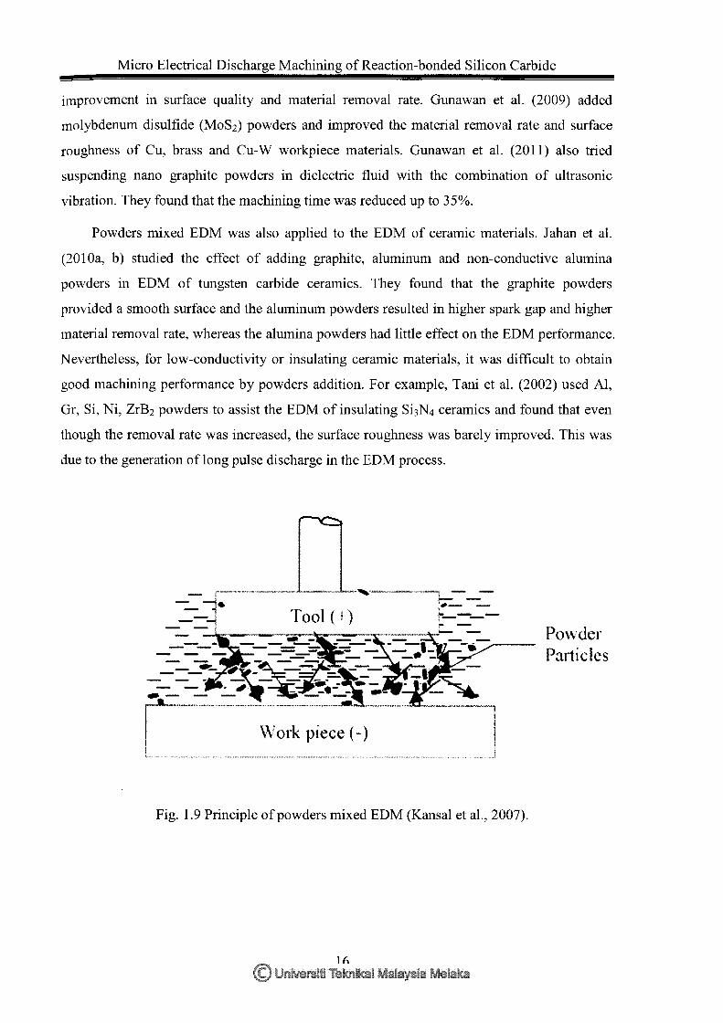
1.3.1 Powders mixed EDM (PMEDM)
The mechanism of powders mixed EDM is different from the conventional EDM with
the pure dielectric fluid. In powders mixed EDM, suitable conductive materials in the form of
powders are mixed into the dielectric fluid, as schematically shown in Fig. 1.9. Under the
influence of high potential intensity, the particles are charged, accelerated, move in the zigzag
fashion and may act as conductors. At the sparking gap between electrode and workpiece, the
particles arrange themselves in the form of chain-like structures and interlock to each other in
the direction of flow of current. The chain formation helps in bridging the discharge gap and
subsequently, the insulating strength of the dielectric fluid decreases due to the bridging effect.
Thus, discharge column easily formed and short circuit is easy to take place, leading to early
explosion in the gap (Kansal et al., 2007). A smaller crater size is created due to the gap
enlargement and high frequency of discharge. The flowing powders additive creates another
bridging effect, discharge column and lastly explosion. The discharging processes repeat
continuously until the final shape is obtained.
Powders mixed EDM proved to be an effective process to improve the machining
efficiency and surface finish of materials. For example, Yeo et al. (2007) added 45-55
nm-sized SiC powders into dielectric and they found that the surface craters became smaller
than those produced in powders free dielectric fluid. Chow et al. (2008) added SiC powders
into pure water as dielectric fluid in the EDM of titanium alloy, and confirmed the
15
Micro Electrical Discharge Machining of Reaction-bonded Silicon Carbide
improvement in surface quality and material removal rate. Gunawan et al. (2009) added
molybdenum disulfide (MoS2) powders and improved the material removal rate and surface
roughness of Cu, brass and Cu-W workpiece materials. Gunawan et al. (2011) also tried
suspending nano graphite powders in dielectric fluid with the combination of ultrasonic
vibration. They found that the machining time was reduced up to 35%.
Powders mixed EDM was also applied to the EDM of ceramic materials. Jahan et al.
(201 Oa, b) studied the effect of adding graphite, aluminum and non-conductive alumina
powders in EDM of tungsten carbide ceramics. They found that the graphite powders
provided a smooth surface and the aluminum powders resulted in higher spark gap and higher
material removal rate, whereas the alumina powders had little effect on the EDM performance.
Nevertheless, for low-conductivity or insulating ceramic materials, it was difficult to obtain
good machining performance by powders addition. For example, Tani et al. (2002) used Al,
Gr, Si, Ni, ZrB2 powders to assist the EDM of insulating Si)N4 ceramics and found that even
though the removal rate was increased, the surface roughness was barely improved. This was
due to the generation of long pulse discharge in the EDM process.
\Vork piece (-)
Fig. 1.9 Principle of powders mixed EDM (Kansal et al., 2007).
Po,vder Particles

Chapter 1 Introduction
1.3.2 Assisting electrode EDM
Pioneer work can be traced to Mohri et al. (1996), who developed a new method of
machining insulating ceramic material by EDM. It is called assisting electrode method. In this
method, a metal plate or metal mesh is arranged on the surface of ceramic insulator as an
assisting electrode. The machining process is shown in Fig. 1.10. In the early stage,
discharges are generated between the metal plate and tool electrode. When the metal plate is
eroded, the dielectric oil is thermally decomposed. Cracked carbon from the working oil and
other electrical conductive compounds from the metal plate, are deposited on the surface of
ceramics. It keeps electrical conductivity on the surface of the workpiece during the
machining. Hence, discharge continues to occur over the ceramics.
By using this method, insulating ceramics such as alumina and Si3N4 have been
machined by sinking EDM (Muttamara et al., 2003; Fukuzawa et al., 2004; Muttamara et al.,
2009). In addition, Tani et al. (2004) and Fukuzawa et al. (2009) fabricated three-dimensional
complex shape successfully on the insulating ShN4 and Zr02 with this assisting electrode
method by WEDM. Fig. 1.11 shows the machining apparatus for the assisting electrode
method by WEDM.
fu-1. d1:c1rod1:
Kerose11e Discharge Colu11111
V .\ssistinl!. !!!!!· !!!!!!!!·!l~C!!if-
1-l' ll'~·t n 1Jc ,,,,,,,,,;,,, = ....
nu ten~ ~~~~~~~~
(a) Discharge for assisting electrode ~ ~
( h l Transition from assisting electrode to the insulating material
(CJ Discharge for insulating material
Fig. 1.10 Machining process of insulating materials using assisting electrode (Fukuzawa et al.,
2004).