toby-l1 series - u-blox · 2016-04-08 · toby-l1 series. 4g lte modules. data sheet. th. the ....
TRANSCRIPT

TOBY-L1 series 4G LTE modules Data Sheet
Abstract Technical data sheet describing TOBY-L1 series LTE wireless modules. The modules are a complete and cost efficient 4G solution offering 100 Mb/s download and 50 Mb/s upload, covering two LTE bands in the compact TOBY form factor.
35.6 x 24.8 x 2.6 mm
www.u-blox.com
UBX-13000868 - R06
TOBY-L1 series - Data Sheet
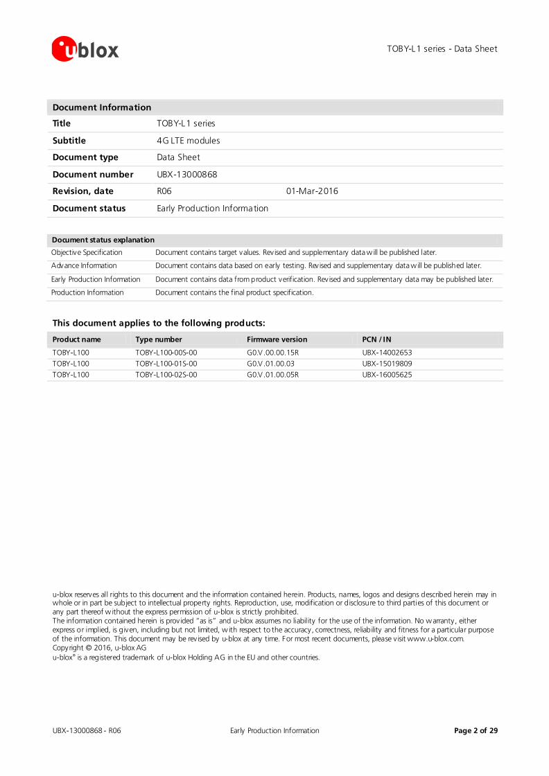
Document Information
Title TOBY-L1 series
Subtitle 4G LTE modules
Document type Data Sheet
Document number UBX-13000868
Revision, date R06 01-Mar-2016
Document status Early Production Information
Document status explanation
Objective Specification Document contains target values. Revised and supplementary data w ill be published later.
Advance Information Document contains data based on early testing. Revised and supplementary data w ill be published later.
Early Production Information Document contains data from product verification. Revised and supplementary data may be published later.
Production Information Document contains the final product specification.
This document applies to the following products:
u-blox reserves all rights to this document and the information contained herein. Products, names, logos and designs described herein may in whole or in part be subject to intellectual property rights. Reproduction, use, modification or disclosure to third parties of this document or any part thereof w ithout the express permission of u-blox is strictly prohibited. The information contained herein is provided “as is” and u-blox assumes no liability for the use of the information. No warranty, either express or implied, is given, including but not limited, w ith respect to the accuracy, correctness, reliability and fitness for a particular purpose of the information. This document may be rev ised by u-blox at any time. For most recent documents, please v isit www.u-blox.com. Copyright © 2016, u-blox AG u-blox® is a registered trademark of u-blox Holding AG in the EU and other countries.
Product name Type number Firmware version PCN / IN
TOBY-L100 TOBY-L100-00S-00 G0.V.00.00.15R UBX-14002653
TOBY-L100 TOBY-L100-01S-00 G0.V.01.00.03 UBX-15019809
TOBY-L100 TOBY-L100-02S-00 G0.V.01.00.05R UBX-16005625
UBX-13000868 - R06 Early Production Information Page 2 of 29

TOBY-L1 series - Data Sheet
Contents Contents............................................................................................................................................. 3
1 Functional description ............................................................................................................. 5 1.1 Overview ................................................................................................................................... 5 1.2 Product features ......................................................................................................................... 5 1.3 Block diagram ............................................................................................................................ 6 1.4 Product description ..................................................................................................................... 7 1.5 AT Command support................................................................................................................. 7
2 Interfaces .................................................................................................................................... 8 2.1 Power Management ................................................................................................................... 8
2.1.1 Module supply input (VCC) ................................................................................................... 8 2.1.2 RTC supply output (V_BCKP) ................................................................................................. 8 2.1.3 Digital I/O interfaces supply output (V_INT) ............................................................................. 8
2.2 RF antenna interfaces .................................................................................................................. 8 2.3 System functions ........................................................................................................................ 8
2.3.1 Module power-on (PWR_ON) ................................................................................................ 8 2.3.2 Module power-off ............................................................................................................... 8 2.3.3 Module reset ....................................................................................................................... 9
2.4 SIM interface.............................................................................................................................. 9 2.5 Data communication................................................................................................................... 9
2.5.1 Universal Serial Bus (USB) ...................................................................................................... 9 2.6 GPIO ....................................................................................................................................... 10
2.6.1 Network Status Indication ................................................................................................... 10
3 Pin Definition ...........................................................................................................................11 3.1 Pin Assignment......................................................................................................................... 11
4 Electrical specifications..........................................................................................................15 4.1 Absolute maximum rating.......................................................................................................... 15
4.1.1 Maximum ESD ................................................................................................................... 15 4.2 Operating conditions................................................................................................................. 16
4.2.1 Operating temperature range .............................................................................................. 16 4.2.2 Supply/Power pins.............................................................................................................. 16 4.2.3 Current consumption ......................................................................................................... 16 4.2.4 RF Performance ................................................................................................................. 17 4.2.5 PWR_ON pin ..................................................................................................................... 18 4.2.6 RESET_N pin ...................................................................................................................... 18 4.2.7 SIM pins............................................................................................................................ 18 4.2.8 USB pins ........................................................................................................................... 19 4.2.9 Generic Digital Interfaces pins ............................................................................................. 19
UBX-13000868 - R06 Early Production Information Contents
Page 3 of 29

TOBY-L1 series - Data Sheet
5 Mechanical specifications .....................................................................................................20
6 Qualification and approvals .................................................................................................21 6.1 Reliability tests.......................................................................................................................... 21 6.2 Approvals ................................................................................................................................ 21
7 Product handling & soldering ..............................................................................................22 7.1 Packaging ................................................................................................................................ 22
7.1.1 Reels ................................................................................................................................ 22 7.1.4 Tapes ............................................................................................................................... 23
7.2 Moisture Sensitivity Levels.......................................................................................................... 24 7.3 Reflow soldering....................................................................................................................... 24 7.4 ESD precautions ....................................................................................................................... 24
8 Labeling and ordering information....................................................................................25 8.1 Product labeling ....................................................................................................................... 25 8.2 Explanation of codes ................................................................................................................. 25 8.3 Ordering information ................................................................................................................ 26
Appendix .........................................................................................................................................27
A Glossary .....................................................................................................................................27
Related documents........................................................................................................................28
Revision history..............................................................................................................................28
Contact .............................................................................................................................................29
UBX-13000868 - R06 Early Production Information Contents
Page 4 of 29
TOBY-L1 series - Data Sheet
1 Functional description
1.1 Overview The TOBY-L1 series comprises LTE-only modules in the very small LGA form-factor (35.6 x 24.8 x 2.6 mm) that are easy to integrate in compact designs. The TOBY-L1 series modules support two LTE-FDD bands.
LTE-only modules offer cost advantages compared to multi-mode (LTE/3G/2G) modules and are optimized for applications using only LTE networks. Additionally, the TOBY-L1 series modules are form-factor compatible with the popular u-blox wireless module families: this allows customers to take the maximum advantage of their hardware and software investments, and provides very short time-to-market.
The modules are dedicated for data transfer, supporting a high-speed USB 2.0 interface. With LTE Category 3 data rates of 100 Mb/s (downlink) and 50 Mb/s (uplink), the modules are ideal for applications requiring the highest data-rates and high-speed internet access. TOBY-L1 series modules are the perfect choice for consumer fixed-wireless terminals, mobile routers and gateways, and applications requiring video streaming. They are also optimally suited for industrial (M2M) applications, such as remote access to video cameras, digital signage, telehealth, security and surveillance systems.
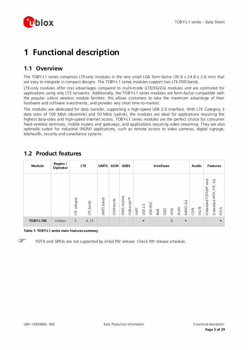
1.2 Product features
Module Region / Operator LTE UMTS GSM GNSS Interfaces Audio Features
LTE
cate
gory
LTE
band
s
UM
TS b
ands
GSM
ban
ds
GN
SS re
ceiv
er
Cel
lLoc
ate™
UA
RT
USB
2.0
USB
HSI
C
RMII
SDIO
GPI
O
Aud
io
MIM
O 2
x2
CSF
B
VoL
TE
Embe
dded
TCP
/UD
P st
ack
Embe
dded
HTT
P, F
TP, S
SL
FOTA
TOBY-L100 Verizon 3 4, 13 • 6 • •
Table 1: TOBY-L1 series main features summary
FOTA and GPIOs are not supported by initial FW release. Check FW release schedule.
UBX-13000868 - R06 Early Production Information Functional description
Page 5 of 29

TOBY-L1 series - Data Sheet
1.3 Block diagram
WirelessBase-bandProcessorMemory
Power Management Unit
26 MHz
32.768 kHz
ANT1
RF Transceiver
ANT2
V_INT (I/O)
V_BCKP
VCC (Supply)
(U)SIM Card
USB
GPIO *
Power On
External Reset
PA
LNA Filter
FilterDuplexer
Filter
PA
LNA Filter
FilterDuplexer
Filter
LNA FilterFilter
LNA FilterFilter
Switch
Switch
Figure 1: TOBY-L100 block diagram
* = GPIOs are not supported by initial FW release.
UBX-13000868 - R06 Early Production Information Functional description
Page 6 of 29

TOBY-L1 series - Data Sheet
1.4 Product description TOBY-L1 series wireless modules provide 4G LTE-only data communication support over two LTE-FDD bands:
• TOBY-L100 is designed for operation on the LTE Verizon network in North America (LTE bands 4, 13), and meets the requirements of Verizon network certification for LTE only devices.
4G LTE Characteristics
3GPP Release 9 - Long Term Evolution (LTE) Evolved Universal Terrest rial Radio Access (E-UTRA) Frequency Div ision Duplex (FDD) Down-Link Multi-Input Multi-Output (MIMO) 2 x 2 antenna support
Band support: • TOBY-L100:
o Band 4: 1710 - 1755 MHz (Tx), 2110 - 2155 MHz (Rx) o Band 13: 777 - 787 MHz (Tx), 746 - 756 MHz (Rx)
Channel bandwidth: • TOBY-L100
o Band 4: 5 MHz, 10 MHz, 15 MHz, 20 MHz o Band 13: 10 MHz
Power class: • Power class 3 (+23 dBm)
Data rate: • LTE category 3: up to 50 Mb/s Up-Link, 100 Mb/s Down-Link
Short Message Serv ice (SMS): • SMS v ia embedded IMS (IP Multimedia Subsystem)
Table 2: TOBY-L1 series LTE characteristics summary
1.5 AT Command support The TOBY-L1 series modules support AT commands according to 3GPP standards TS 27.007 [1], 27.005 [2] and the u-blox AT command extension.
For the complete list of all supported AT commands and their syntax, refer to the TOBY-L1 / MPCI-L1 Series AT Commands Manual [3].
RIL (Radio Interface Layer) software for Android is available for TOBY-L1 series modules free of charge.
UBX-13000868 - R06 Early Production Information Functional description
Page 7 of 29

TOBY-L1 series - Data Sheet
2 Interfaces
2.1 Power Management
2.1.1 Module supply input (VCC)
TOBY-L1 series modules must be supplied through the VCC pins by a DC power supply. Voltage must be stable, because during operation the current drawn from VCC can vary significantly, based on the power consumption profile of the LTE system (described in the TOBY-L1 / MPCI-L1 Series System Integration Manual [4]).
2.1.2 RTC supply output (V_BCKP)
When VCC voltage is within the valid operating range, the internal Power Management Unit (PMU) supplies the Real Time Clock (RTC) and the same supply voltage is available on V_BCKP pin.
2.1.3 Digital I/O interfaces supply output (V_INT)
TOBY-L1 series modules provide an internally generated supply rail 1.8 V output for external interfaces (V_INT). This can be used in place of an external discrete regulator.
2.2 RF antenna interfaces The modules have two RF pads with a characteristic impedance of 50 Ω. The primary antenna pin (ANT1) supports both Tx and Rx, providing the main antenna interface, while the secondary antenna pin (ANT2) supports Rx only for the MIMO 2x2 configuration.
2.3 System functions
2.3.1 Module power-on (PWR_ON)
TOBY-L1 series can be switched on by:
• Forcing to the low level the PWR_ON pin, normally high with external pull-up, for a valid time period (refer to section 4.2.5), when the applied VCC voltage is within the valid operating range.
• Alternately, the PWR_ON pin can be forced to the low level before VCC has been applied and then held low for a valid time period (refer to section 4.2.5) after VCC has been applied.
The PWR_ON pin requires an external pull-up resistor to set its value to logic high and may not be left floating. The line should be driven by open drain, open collector or contact s witch.
2.3.2 Module power-off
TOBY-L1 series can be switched off by:
• AT+CPWROFF command (see TOBY-L1 / MPCI-L1 Series AT Commands Manual [3]). The current parameter settings are saved in the module’s non-vola tile memory and a proper network detach is performed.
An abrupt shutdown occurs on TOBY-L1 series modules when a low level is applied on the RESET_N pin, which is normally set high by internal pull-up, for a valid time period (see section 4.2.6). The current parameter settings are not saved in the module’s non-volatile memory and proper network detach is not performed. The line should be driven by open drain, open collector or contact switch.
UBX-13000868 - R06 Early Production Information Interfaces
Page 8 of 29

TOBY-L1 series - Data Sheet
An abrupt under-voltage shutdown occurs on TOBY-L1 series modules when the VCC supply is removed, but in this case it is not possible to perform the storing of the current parameter settings in the module’s non-volatile memory as well as the proper network detach.
2.3.3 Module reset
TOBY-L1 series can be reset (rebooted) by:
• AT+CFUN command (see TOBY-L1 / MPCI-L1 Series AT Commands Manual [3]). This causes an “internal” or “software” reset of the module. The current parameter settings are saved in the module’s non-volatile memory and a proper network detach is performed.
An abrupt “external” or “hardware” reset occurs when a low level is applied to the RESET_N pin, which is normally set high by internal pull-up, for a valid time period (see section 4.2.6) and then forcing to the low level the PWR_ON pin, normally high with external pull-up, for a valid time period (see section 4.2.5). In this case, the current parameter settings are not saved in the module’s non-volatile memory and a proper network detach is not performed. The lines should be driven by open drain, open collector or contact switch.
2.4 SIM interface A SIM interface is provided on the VSIM, SIM_IO, SIM_CLK, SIM_RST pads: the high-speed SIM/ME interface is implemented as well as the automatic detection of the required SIM supporting voltage.
Both 1.8 V and 3 V SIM types are supported (1.8 V and 3 V ME). Activation and deactivation with automatic voltage switch from 1.8 V to 3 V is implemented, according to ISO-IEC 7816-3 specifications. The SIM driver supports the PPS procedure for baud-rate selection, according to the values proposed by the SIM card/chip.
2.5 Data communication TOBY-L1 series provides the following serial communication interfaces for concurrent communication via the AT command interface and Traffic Data:
• One high-speed USB 2.0 compliant interface
2.5.1 Universal Serial Bus (USB)
TOBY-L1 series includes a high-speed USB 2.0 compliant interface with maximum throughput of 480 Mb/s. The module itself acts as a USB device and can be connected to any USB host that has the necessary drivers installed. For driver details, refer to the TOBY-L1 / MPCI-L1 Series System Integration Manual [4].
The USB is the main interface for transferring high speed data between TOBY-L1 series and a host processor. USB_D+/USB_D- carry the USB serial data and signaling.
TOBY-L1 modules open two USB CDCs (Communications Device Class):
• Network Adapters : Remote NDIS based Internet Sharing Device ( Ethernet connection )
• Port : Gadget Serial ( AT commands )
UBX-13000868 - R06 Early Production Information Interfaces
Page 9 of 29

TOBY-L1 series - Data Sheet
2.6 GPIO TOBY-L1 series modules provide 6 pins that can be configured as general purpose input/output (GPIO).
The network status indication over the GPIO1 pin is the only function that is supported by the initial firmware release. Check firmware release schedule for possible future GPIOs.
2.6.1 Network Status Indication
The network indication feature can be enabled over the GPIO1 pin through a custom AT command. This is used to indicate the network status: registered home network, registered roaming, data call enabled, no service (for more details refer to the TOBY-L1 / MPCI-L1 Series System Integration Manual [4] and to the TOBY-L1 / MPCI-L1 Series AT commands manual [3] (+UGPIOC).
UBX-13000868 - R06 Early Production Information Interfaces
Page 10 of 29

TOBY-L1 series - Data Sheet
3 Pin Definition
3.1 Pin Assignment
11
10
7
5
4
2
1
21
19
18
16
15
13
12
29
27
26
24
23
8
6
3
22
20
17
14
28
25
9
65
66
69
71
72
74
75
55
57
58
60
61
63
64
47
49
50
52
53
68
70
73
54
56
59
62
48
51
67
RSVD
RSVD
GND
VCC
VCC
GND
RSVD
RSVD
SIM_IO
SIM_RST
GPIO5
GPIO6
RSVD
RSVD
RSVD
RSVD
RSVD
RSVD
RSVD
RSVD
VCC
GND
RSVD
SIM_CLK
VSIM
RSVD
RSVD
RSVD
RSVD
RSVD
RSVD
RSVD
V_INT
RSVD
GND
RSVD
GPIO1
RSVD
RSVD
RSVD
RSVD
RSVD
RSVD
RSVD
USB_D-
RSVD
GPIO3
RESET_N
RSVD
RSVD
V_BCKP
GPIO2
PWR_ON
RSVD
RSVD
USB_D+
GPIO4
RSVD
90 91 92787776
93100
79 80 83 85 86 88 8982 84 8781
GN
D
RSV
D
GN
D
GN
D
RSV
D
GN
D
GN
D
GN
D
GN
D
GN
D
GN
D
GN
D
GN
D
GN
D
RSV
D
AN
T2
AN
T1
32 31 30444546
145152
43 42 39 37 36 34 3340 38 3541
GN
D
RSV
D
GN
D
GN
D
RSV
D
GN
D
RSV
D
RSV
D
RSV
D
RSV
D
RSV
D
RSV
D
RSV
D
RSV
D
RSV
D
RSV
D
RSV
D
99 98 97 96 95 94
106 105 104 103 102 101
108 107
124 123
130 129 128 127 126 125
136 135 134 133 132 131
138 137
144 143 142 141 140 139
151 150 149 148 147 146
114 113 112 111 110 109
120 119 118 117 116 115
122 121
Pin 93-152: GND
TOBY-L1Top view
Figure 2: TOBY-L1 series pin assignment (Top view)
UBX-13000868 - R06 Early Production Information Pin Definition
Page 11 of 29
TOBY-L1 series - Data Sheet
No Name Power domain
I/O Description Remarks
1 RSVD - N/A RESERVED pin Leave unconnected.
2 GND GND N/A Ground All GND pads must be connected to ground.
3 V_BCKP - O Real Time Clock supply output
2.5 V (typical) generated by the module when VCC supply voltage is w ithin valid operating range. See section 4.2.2 for detailed electrical specs.
4 RSVD - N/A RESERVED pin Leave unconnected.
5 V_INT - O Digital I/O Interfaces supply output
1.8 V (typical) generated by the module when it is sw itched-on. See section 4.2.2 for detailed electrical specs.
6 RSVD - N/A RESERVED pin Leave unconnected.
7 RSVD - N/A RESERVED pin Leave unconnected.
8 RSVD - N/A RESERVED pin Leave unconnected.
9 RSVD - N/A RESERVED pin Leave unconnected.
10 RSVD - N/A RESERVED pin Leave unconnected.
11 RSVD - N/A RESERVED pin Leave unconnected.
12 RSVD - N/A RESERVED pin Leave unconnected.
13 RSVD - N/A RESERVED pin Leave unconnected.
14 RSVD - N/A RESERVED pin Leave unconnected.
15 RSVD - N/A RESERVED pin Leave unconnected.
16 RSVD - N/A RESERVED pin Leave unconnected.
17 RSVD - N/A RESERVED pin Leave unconnected.
18 RSVD - N/A RESERVED pin Leave unconnected.
19 RSVD - N/A RESERVED pin Leave unconnected.
20 PWR_ON POS I Power-on input The PWR_ON pin has high input impedance: don’t leave it floating in noisy environment (an external pull-up resistor is required). See section 4.2.5 for detailed electrical specs.
21 GPIO1 GDI I/O GPIO Note: not supported by initial FW release. See section 4.2.9 for detailed electrical specs.
22 GPIO2 GDI I/O GPIO Note: not supported by initial FW release. See section 4.2.9 for detailed electrical specs.
23 RESET_N ERS I External reset input Internal 10 kΩ pull-up resistor to V_BCKP. See section 4.2.6 for detailed electrical specs.
24 GPIO3 GDI I/O GPIO Note: not supported by initial FW release. See section 4.2.9 for detailed electrical specs.
25 GPIO4 GDI I/O GPIO Note: not supported by initial FW release. See section 4.2.9 for detailed electrical specs.
26 RSVD - N/A RESERVED pin Leave unconnected.
27 USB_D- USB I/O USB Data Line D- 90 Ω nominal differential impedance Pull-up, pull-down and series resistors as required by the USB Revision 2.0 specification [5] are part of the USB pad driver and need not be provided externally . See section 4.2.8 for detailed electrical specs.
28 USB_D+ USB I/O USB Data Line D+ 90 Ω nominal differential impedance Pull-up, pull-down and series resistors as required by the USB Revision 2.0 specification [5] are part of the USB pad driver and need not be provided externally . See section 4.2.8 for detailed electrical specs.
29 RSVD - N/A RESERVED pin Leave unconnected.
30 GND GND N/A Ground All GND pads must be connected to ground.
31 RSVD - N/A RESERVED pin Leave unconnected.
32 GND GND N/A Ground All GND pads must be connected to ground.
33 RSVD - N/A RESERVED pin Leave unconnected.
34 RSVD - N/A RESERVED pin Leave unconnected.
35 RSVD - N/A RESERVED pin Leave unconnected.
UBX-13000868 - R06 Early Production Information Pin Definition
Page 12 of 29

TOBY-L1 series - Data Sheet
No Name Power domain
I/O Description Remarks
36 RSVD - N/A RESERVED pin Leave unconnected.
37 RSVD - N/A RESERVED pin Leave unconnected.
38 RSVD - N/A RESERVED pin Leave unconnected.
39 RSVD - N/A RESERVED pin Leave unconnected.
40 RSVD - N/A RESERVED pin Leave unconnected.
41 RSVD - N/A RESERVED pin Leave unconnected.
42 RSVD - N/A RESERVED pin Leave unconnected.
43 RSVD - N/A RESERVED pin Leave unconnected.
44 GND GND N/A Ground All GND pads must be connected to ground.
45 RSVD - N/A RESERVED pin Leave unconnected.
46 GND GND N/A Ground All GND pads must be connected to ground.
47 RSVD - N/A RESERVED pin Leave unconnected.
48 RSVD - N/A RESERVED pin Leave unconnected.
49 RSVD - N/A RESERVED pin Leave unconnected.
50 RSVD - N/A RESERVED pin Leave unconnected.
51 RSVD - N/A RESERVED pin Leave unconnected.
52 RSVD - N/A RESERVED pin Leave unconnected.
53 RSVD - N/A RESERVED pin Leave unconnected.
54 RSVD - N/A RESERVED pin Leave unconnected.
55 RSVD - N/A RESERVED pin Leave unconnected.
56 SIM_CLK SIM O SIM clock See section 4.2.7 for detailed electrical specs.
57 SIM_IO SIM I/O SIM data Internal 4.7 kΩ pull-up resistor to VSIM. See section 4.2.7 for detailed electrical specs.
58 SIM_RST SIM O SIM reset See section 4.2.7 for detailed electrical specs.
59 VSIM - O SIM supply output VSIM = 1.8 V typical or 3.0 V typical generated by the module according to the SIM card/chip voltage type. See section 4.2.2 for detailed electrical specs.
60 GPIO5 GDI I/O GPIO Note: not supported by initial FW release. See section 4.2.9 for detailed electrical specs.
61 GPIO6 GDI I/O GPIO Note: not supported by initial FW release. See section 4.2.9 for detailed electrical specs.
62 RSVD - N/A RESERVED pin Leave unconnected.
63 RSVD - N/A RESERVED pin Leave unconnected.
64 RSVD - N/A RESERVED pin Leave unconnected.
65 RSVD - N/A RESERVED pin Leave unconnected.
66 RSVD - N/A RESERVED pin Leave unconnected.
67 RSVD - N/A RESERVED pin Leave unconnected.
68 RSVD - N/A RESERVED pin Leave unconnected.
69 GND GND N/A Ground All GND pads must be connected to ground.
70 VCC VCC I Module supply input All VCC pins must be connected to external supply. See sections 4.2.2 / 4.2.3 for detailed electrical specs.
71 VCC VCC I Module supply input All VCC pins must be connected to external supply. See sections 4.2.2 / 4.2.3 for detailed electrical specs.
72 VCC VCC I Module supply input All VCC pins must be connected to external supply. See sections 4.2.2 / 4.2.3 for detailed electrical specs.
73 GND GND N/A Ground All GND pads must be connected to ground.
74 GND GND N/A Ground All GND pads must be connected to ground.
75 RSVD - N/A RESERVED pin Leave unconnected.
76 GND GND N/A Ground All GND pads must be connected to ground.
77 RSVD - N/A RESERVED pin Leave unconnected.
78 GND GND N/A Ground All GND pads must be connected to ground.
79 GND GND N/A Ground All GND pads must be connected to ground.
80 GND GND N/A Ground All GND pads must be connected to ground.
UBX-13000868 - R06 Early Production Information Pin Definition
Page 13 of 29

TOBY-L1 series - Data Sheet
No Name Power domain
I/O Description Remarks
81 ANT1 ANT I/O Primary antenna 50 Ω nominal characteristic impedance Main Tx / Rx antenna interface. See section 4.2.4 for detailed electrical specs.
82 GND GND N/A Ground All GND pads must be connected to ground.
83 GND GND N/A Ground All GND pads must be connected to ground.
84 RSVD - N/A RESERVED pin Leave unconnected.
85 GND GND N/A Ground All GND pads must be connected to ground.
86 GND GND N/A Ground All GND pads must be connected to ground.
87 ANT2 ANT I Secondary antenna 50 Ω nominal characteristic impedance Rx only for the MIMO 2x2 configuration. See section 4.2.4 for detailed electrical specs.
88 GND GND N/A Ground All GND pads must be connected to ground.
89 GND GND N/A Ground All GND pads must be connected to ground.
90 GND GND N/A Ground All GND pads must be connected to ground.
91 RSVD - N/A RESERVED pin Leave unconnected.
92 GND GND N/A Ground All GND pads must be connected to ground.
93-152 GND GND N/A Ground All GND pads must be connected to ground.
Table 3: TOBY-L1 series pin out
For more information about the pinout, see the TOBY-L1 / MPCI-L1 Series System Integration Manual [4].
See Appendix A for an explanation of abbreviations and terms used.
UBX-13000868 - R06 Early Production Information Pin Definition
Page 14 of 29
TOBY-L1 series - Data Sheet
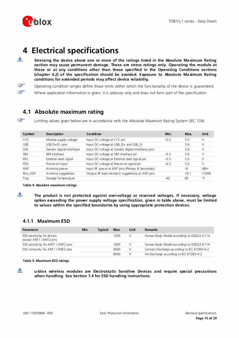
4 Electrical specifications Stressing the device above one or more of the ratings listed in the Absolute Maximum Rating
section may cause permanent damage. These are stress ratings only. Operating the module at these or at any conditions other than those specified in the Operating Conditions sections (chapter 4.2) of the specification should be avoided. Exposure to Absolute Maximum Rating conditions for extended periods may affect device reliability.
Operating condition ranges define those limits within which the functionality of the device is guaranteed.
Where application information is given, it is advisory only and does not form part of the specification.
4.1 Absolute maximum rating Limiting values given below are in accordance with the Absolute Maximum Rating System (IEC 134).
Symbol Description Condition Min. Max. Unit
VCC Module supply voltage Input DC voltage at VCC pin -0.3 5.0 V
USB USB D+/D- pins Input DC voltage at USB_D+ and USB_D- 3.6 V
GDI Generic digital interfaces Input DC voltage at Generic digital interfaces pins 3.6 V
SIM SIM interface Input DC voltage at SIM interface pin -0.3 3.6 V
ERS External reset signal Input DC voltage at External reset signal pin -0.3 5.0 V
POS Power-on input Input DC voltage at Power-on signal pin -0.3 5.0 V
ANT Antenna power Input RF power at ANT pins (Primary & Secondary) -8 dBm
Rho_ANT Antenna ruggedness Output RF load mismatch ruggedness at ANT pins 10:1 VSWR
Tstg Storage Temperature -40 85 °C
Table 4: Absolute maximum ratings
The product is not protected against overvoltage or reversed voltages. If necessary, voltage spikes exceeding the power supply voltage specification, given in table above, must be limited to values within the specified boundaries by using appropriate protection devices.
4.1.1 Maximum ESD
Parameter Min Typical Max Unit Remarks
ESD sensitiv ity for all pins except ANT1 / ANT2 pins
1000 V Human Body Model according to JESD22-A114
ESD sensitiv ity for ANT1 / ANT2 pins 1000 V Human Body Model according to JESD22-A114
ESD immunity for ANT1 / ANT2 pins 4000 V Contact Discharge according to IEC 61000-4-2
8000 V Air Discharge according to IEC 61000-4-2
Table 5: Maximum ESD ratings
u-blox wireless modules are Electrostatic Sensitive Devices and require special precautions when handling. See Section 7.4 for ESD handling instructions.
UBX-13000868 - R06 Early Production Information Electrical specifications
Page 15 of 29

TOBY-L1 series - Data Sheet
4.2 Operating conditions Unless otherwise indicated, all operating condition specifications are at an ambient temperature of 25°C.
Operation beyond the operating conditions is not recommended and extended exposure beyond them may affect device reliability.
4.2.1 Operating temperature range
Parameter Min. Typical Max. Unit Remarks
Normal operating temperature -10 +25 +55 °C Normal operating temperature range (fully functional and meet 3GPP specifications)
Extended operating temperature -40 +85 °C Extended operating temperature range (Occasional deviations from 3GPP specifications may occur, though the module is functional)
Table 6: Environmental conditions
4.2.2 Supply/Power pins
Symbol Parameter Min. Typical Max. Unit
VCC Module supply input voltage 3.40 4.00 4.50 V
Table 7: Input characteristics of Supply/Power pins
Symbol Parameter Min. Typical Max. Unit
VSIM SIM supply output voltage 1.75 1.80 1.85 V
2.92 3.00 3.08 V
V_BCKP RTC supply output voltage 2.44 2.50 2.56 V
I_BCKP RTC supply output current capability 3 mA
V_INT Digital I/O Interfaces supply output voltage 1.75 1.80 1.85 V
I_INT Digital I/O Interfaces supply output current capability 70 mA
Table 8: Output characteristics of Supply/Power pins
4.2.3 Current consumption
Mode Condition Current consumption1
Power off Module is sw itched off < 40 µA
Power sav ing enabled (Cyclic Idle/Active-Mode)
Module is registered w ith the network, w ith a paging period of 2.56 s. USB interface in the suspend state.
< 3 mA
Connected mode Maximum Tx power (23 dBm typical) < 800 mA
Table 9: Module VCC current consumption
1 Maximum values for module current consumption through the VCC pins in the listed conditions, at 25 °C, w ith VCC = 4.0 V . It is assumed that no significant load is connected to any pin.
UBX-13000868 - R06 Early Production Information Electrical specifications
Page 16 of 29

TOBY-L1 series - Data Sheet
4.2.4 RF Performance
Parameter Min. Max. Unit Remarks
Frequency range Band 4
Uplink 1710 1755 MHz Module transmit
Downlink 2110 2155 MHz Module receive
Frequency range Band 13
Uplink 777 787 MHz Module transmit
Downlink 746 756 MHz Module receive
Table 10: Operating RF frequency bands
Parameter Min. Typical Max. Unit Remarks
Receiver input sensitiv ity Band 4
-108 dBm Channel bandwidth = 1.4 MHz
-105 dBm Channel bandwidth = 5 MHz
-103 dBm Channel bandwidth = 10 MHz
-101 dBm Channel bandwidth = 15 MHz
-100 dBm Channel bandwidth = 20 MHz
Receiver input sensitiv ity Band 13
-105 dBm Channel bandwidth = 5 MHz
-103 dBm Channel bandwidth = 10 MHz
Condition: 50 Ω source, QPSK modulation, Dual receiver
Table 11: Receiver sensitivity performance
Parameter Min. Typical Max. Unit Remarks
Maximum output power Band 4
23.0 dBm
Maximum output power Band 13
23.0 dBm
Condition: 50 Ω output load, All channel bandwidths
Table 12: Transmitter maximum output power
UBX-13000868 - R06 Early Production Information Electrical specifications
Page 17 of 29

TOBY-L1 series - Data Sheet
4.2.5 PWR_ON pin
Pin Name Parameter Min. Typical Max. Unit Remarks
PWR_ON Internal supply for Power-On Input Signal
2.50 V V_BCKP
L-level input -0.10 0.60 V High input impedance (no internal pull-up)
H-level input 2.20 4.70 V High input impedance (no internal pull-up)
L-level input current -9 µA
PWR_ON low time 5 s Low level to sw itch-on the module
Table 13: PWR_ON pin characteristics
4.2.6 RESET_N pin
Pin Name Parameter Min. Typical Max. Unit Remarks
RESET_N Internal supply for External Reset Input Signal
2.50 V V_BCKP
L-level input 0.00 0.40 V
H-level input 1.10 2.60 V
L-level input current -250 µA
Pull-up resistance 10 kΩ Internal pull-up to RTC supply (V_BCKP)
RESET_N low time 1 s Low pulse to sw itch-off the module
Table 14: RESET_N pin characteristics
4.2.7 SIM pins
The SIM pins are a dedicated interface to the external SIM card/chip. The electrical characteristics fulfill regulatory specification requirements. The values in Table 15 are for information only.
Parameter Min. Typical Max. Unit Remarks
Input characteristic: Low-level -0.10 0.45 V VSIM = 1.8 V
-0.10 0.75 V VSIM = 3.0 V
Input characteristic: High-level 1.53 2.10 V VSIM = 1.8 V
2.55 3.30 V VSIM = 3.0 V
Output characteristics: High-level 0.00 0.40 V VSIM = 1.8 V, Max value at IOL = +8 mA
0.00 0.80 V VSIM = 3.0 V, Max value at IOL = +8 mA
Output characteristics: High-level 1.53 1.80 V VSIM = 1.8 V, Min value at IOH
= -8 mA
2.55 3.00 V VSIM = 3.0 V, Min value at IOH
= -8 mA
Input / Output leakage current 10 µA
Internal pull-up resistor on SIM_IO 4.7 kΩ Internal pull-up to VSIM supply
Clock frequency on SIM_CLK 5 MHz
Table 15: SIM pins characteristics
UBX-13000868 - R06 Early Production Information Electrical specifications
Page 18 of 29

TOBY-L1 series - Data Sheet
4.2.8 USB pins
USB data lines (USB_D+ / USB_D-) are compliant to the USB 2.0 high-speed specification. Refer to the Universal Serial Bus Revision 2.0 specification [5] for detailed electrical characteristics. The values reported in Table 16 related to USB 2.0 high-speed physical layer specifications are for information only.
Parameter Min. Typical Max. Unit Remarks
High-speed squelch detection threshold (input differential signal amplitude)
100 150 mV
High speed disconnect detection threshold (input differential signal amplitude)
525 625 mV
High-speed data signaling input common mode voltage range
-50 500 mV
High-speed idle output level -10 10 mV
High-speed data signaling output high level 360 440 mV
High-speed data signaling output low level -10 10 mV
Chirp J level (output differential voltage) 700 1100 mV
Chirp K level (output differential voltage) -900 -500 mV
Table 16: USB pins characteristics
4.2.9 Generic Digital Interfaces pins
Parameter Min Typical Max Unit Remarks
Internal supply for GDI domain 1.80 V Digital I/O Interfaces supply (V_INT)
Input characteristic: Low-level -0.10 0.45 V
Input characteristic: High-level 1.53 2.10 V
Output characteristics: Low-level 0.00 0.40 V Max value at IOL = +8 mA
Output characteristics: High-level 1.53 1.80 V Min value at IOH
= -8 mA
Input/Output leakage current 10 µA
Internal pull-up resistance 30 65 kΩ
Internal pull-down resistance 32 91 kΩ
Table 17: GDI pins characteristics
UBX-13000868 - R06 Early Production Information Electrical specifications
Page 19 of 29

TOBY-L1 series - Data Sheet
5 Mechanical specifications
C
I
AG H1 J1D F
K M1 M1 M2 P2
B G
H1J1
H2J2
J2H2
ANT1 pin
O
O
L
N
H2J2
J2H2
ANT2 pin
M1 M1 M3
I
I
I
O H1
J1
J1
J1
E
P3
F
P1
H1
I
O
Pin 1 Indicator
Figure 3: TOBY-L1 series dimensions (Bottom and Sides views)
Parameter Description Typical Tolerance
A Module Height [mm] 35.6 (1401.6 mil) +0.20/-0.20 (+7.9/-7.9 mil) B Module Width [mm] 24.8 (976.4 mil) +0.20/-0.20 (+7.9/-7.9 mil) C Module Thickness [mm] 2.6 (102.4 mil) +0.27/-0.17 (+10.6/-6.7 mil) D Horizontal Edge to Lateral Pin Pitch [mm] 2.4 (94.5 mil) +0.20/-0.20 (+7.9/-7.9 mil) E Vertical Edge to Lateral Pin Pitch [mm] 2.25 (88.6 mil) +0.20/-0.20 (+7.9/-7.9 mil) F Edge to Lateral Pin Pitch [mm] 1.45 (57.1 mil) +0.20/-0.20 (+7.9/-7.9 mil) G Lateral Pin to Pin Pitch [mm] 1.1 (43.3 mil) +0.02/-0.02 (+0.8/-0.8 mil) H1 Lateral Pin Height [mm] 0.8 (31.5 mil) +0.02/-0.02 (+0.8/-0.8 mil) H2 Lateral Pin close to ANT1 and ANT2 Height [mm] 0.9 (35.4 mil) +0.02/-0.02 (+0.8/-0.8 mil) I Lateral Pin Width [mm] 1.5 (59.1 mil) +0.02/-0.02 (+0.8/-0.8 mil) J1 Lateral Pin to Pin Distance [mm] 0.3 (11.8 mil) +0.02/-0.02 (+0.8/-0.8 mil) J2 Lateral Pin to Pin close to ANT Distance [mm] 0.2 (7.9 mil) +0.02/-0.02 (+0.8/-0.8 mil) K Horizontal Edge to Central Pin Pitch [mm] 3.15 (124.0 mil) +0.20/-0.20 (+7.9/-7.9 mil) L Vertical Edge to Central Pin Pitch [mm] 7.15 (281.5 mil) +0.20/-0.20 (+7.9/-7.9 mil) M1 Central Pin to Pin Horizontal Pitch [mm] 1.8 (70.9 mil) +0.02/-0.02 (+0.8/-0.8 mil) M2 Central Pin to Pin Horizontal Pitch [mm] 5.2 (204.7 mil) +0.02/-0.02 (+0.8/-0.8 mil) M3 Central Pin to Pin Horizontal Pitch [mm] 4.5 (177.2 mil) +0.02/-0.02 (+0.8/-0.8 mil) N Central Pin to Pin Vertical Pitch [mm] 2.1 (82.7 mil) +0.02/-0.02 (+0.8/-0.8 mil) O Central Pin Height and Width [mm] 1.1 (43.3 mil) +0.02/-0.02 (+0.8/-0.8 mil) P1 Horizontal Edge to Corner Pin Pitch [mm] 1.1 (43.3 mil) +0.20/-0.20 (+7.9/-7.9 mil) P2 Horizontal Edge to Corner Pin Pitch [mm] 1.25 (49.2 mil) +0.20/-0.20 (+7.9/-7.9 mil) P3 Horizontal Edge to Corner Pin Pitch [mm] 2.85 (112.2 mil) +0.20/-0.20 (+7.9/-7.9 mil) Weight Module Weight [g] < 7
Table 18: TOBY-L1 series dimensions
UBX-13000868 - R06 Early Production Information Mechanical specifications
Page 20 of 29

TOBY-L1 series - Data Sheet
6 Qualification and approvals
6.1 Reliability tests Tests for product family qualifications according to ISO 16750 “Road vehicles - Environmental conditions and testing for electrical and electronic equipment“, and appropriate standards.
6.2 Approvals
Products marked with this lead-free symbol on the product label comply with the "Directive 2002/95/EC of the European Parliament and the Council on the Restriction of Use of certain Hazardous Substances in Electrical and Electronic Equipment" (RoHS).
TOBY-L1 series modules are RoHS compliant.
No natural rubbers, hygroscopic materials, or materials containing asbestos are employed.
For the complete list of approvals and for specific details on all country and network operators certifications please refer to our website www.u-blox.com.
UBX-13000868 - R06 Early Production Information Qualification and approvals
Page 21 of 29

TOBY-L1 series - Data Sheet
7 Product handling & soldering
7.1 Packaging TOBY-L1 series modules are delivered as hermetically sealed, reeled tapes to enable efficient production, production lot set-up and tear-down. For more information about packaging, see the u-blox Package Information Guide [6].
7.1.1 Reels
TOBY-L1 series modules are deliverable in quantities of 150 pcs on a reel. The modules are delivered on the reel type B, as described in Figure 4.
Figure 4: TOBY-L1 series modules reel type B
Parameter Specification
Reel Type Described in F igure 4 above
Delivery Quantity 150
Table 19: Reel information for TOBY-L1 series modules
Quantities of less than 150 pieces are also available. Contact u-blox for more information.
UBX-13000868 - R06 Early Production Information Product handling & soldering
Page 22 of 29

TOBY-L1 series - Data Sheet
7.1.2 Tapes
Figure 5 shows the position and the orientation of TOBY-L1 series modules as they are delivered on the tape. The dimensions of the tapes are specified in Table 20.
Figure 5: Orientation for TOBY-L1 series modules on tape
Table 20: TOBY-L1 series modules tape
UBX-13000868 - R06 Early Production Information Product handling & soldering
Page 23 of 29

TOBY-L1 series - Data Sheet
7.2 Moisture Sensitivity Levels
TOBY-L1 series modules are Moisture Sensitive Devices (MSD) in accordance to the IPC/JEDEC specification.
The Moisture Sensitivity Level (MSL) relates to the packaging and handling precautions required. TOBY-L1 series modules are rated at MSL level 4. For more information regarding moisture sensitivity levels, labeling, storage and drying see the u-blox Package Information Guide [6].
For MSL standard see IPC/JEDEC J-STD-020 (can be downloaded from www.jedec.org).
7.3 Reflow soldering Reflow profiles are to be selected according to u-blox recommendations (see TOBY-L1 / MPCI-L1 Series System Integration Manual [4]).
Failure to observe these recommendations can result in severe damage to the device!
7.4 ESD precautions
TOBY-L1 series modules contain highly sensitive electronic circuitry and are Electrostatic Sensitive Devices (ESD). Handling TOBY-L1 series modules without proper ESD protection may destroy or damage them permanently.
TOBY-L1 series modules are Electrostatic Sensitive Devices (ESD) and require special ESD precautions typically applied to ESD sensitive components.
Table 5 reports the maximum ESD ratings of the TOBY-L1 series modules.
Proper ESD handling and packaging procedures must be applied throughout the processing, handling and operation of any application that incorporates TOBY-L1 series module.
ESD precautions should be implemented on the application board where the module is mounted, as described in the TOBY-L1 / MPCI-L1 Series System Integration Manual [4].
Failure to observe these recommendations can result in severe damage to the device!
UBX-13000868 - R06 Early Production Information
Page 24 of 29

TOBY-L1 series - Data Sheet
8 Labeling and ordering information
8.1 Product labeling
The label on u-blox modules includes important product information. The location of the product type number is shown in Figure 6.
Figure 6: Location of product type number on TOBY-L1 series module label
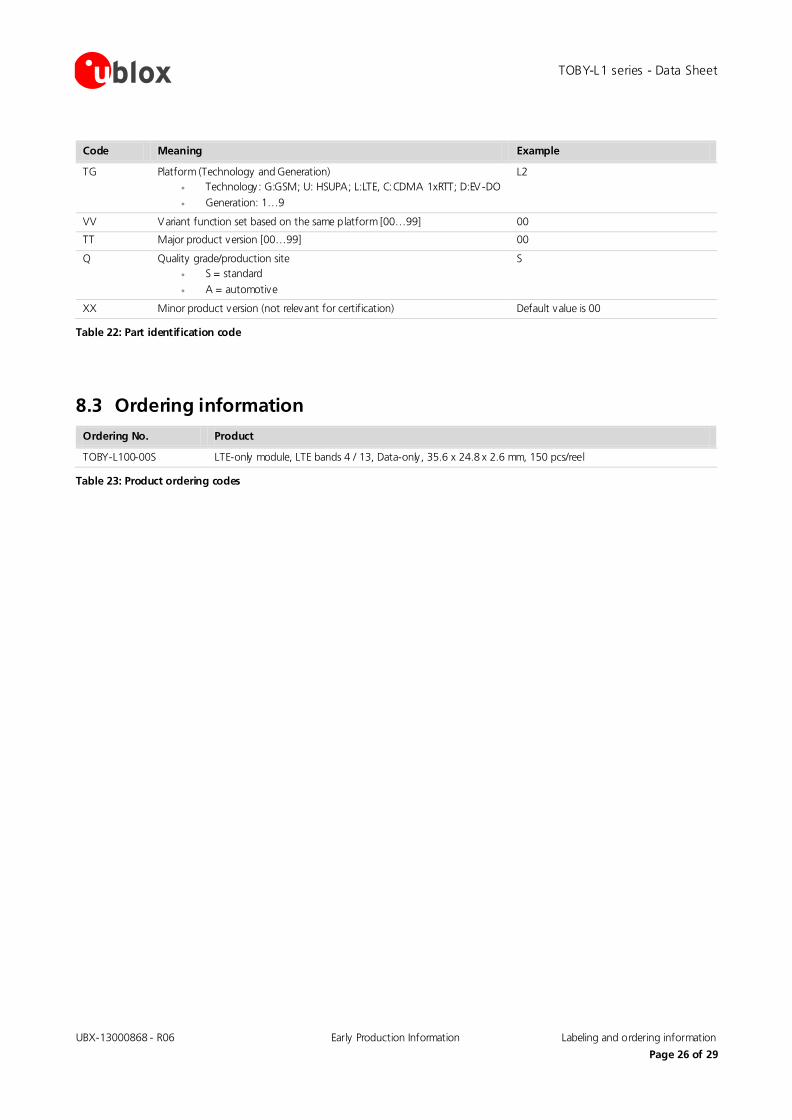
8.2 Explanation of codes Three different product code formats are used. The Product Name is used in documentation such as this data sheet and identifies all u-blox products, independent of packaging and quality grade. The Ordering Code includes options and quality, while the Type Number includes the hardware and firmware versions. Table 21 details these 3 different formats:
Format Structure
Product Name TOBY-TGVV
Ordering Code TOBY-TGVV-TTQ
Type Number TOBY-TGVV-TTQ-XX
Table 21: Product Code Formats
The parts of the product code are explained in Table 22.
Type Number
UBX-13000868 - R06 Early Production Information Labeling and ordering information
Page 25 of 29
TOBY-L1 series - Data Sheet
Code Meaning Example
TG Platform (Technology and Generation) • Technology: G:GSM; U: HSUPA; L:LTE, C:CDMA 1xRTT; D:EV-DO
• Generation: 1…9
L2
VV Variant function set based on the same platform [00…99] 00
TT Major product version [00…99] 00
Q Quality grade/production site • S = standard
• A = automotive
S
XX Minor product version (not relevant for certification) Default value is 00
Table 22: Part identification code
8.3 Ordering information Ordering No. Product
TOBY-L100-00S LTE-only module, LTE bands 4 / 13, Data-only, 35.6 x 24.8 x 2.6 mm, 150 pcs/reel
Table 23: Product ordering codes
UBX-13000868 - R06 Early Production Information Labeling and ordering information
Page 26 of 29

TOBY-L1 series - Data Sheet
Appendix
A Glossary
Name Definition
CSFB Circuit Sw itched Fall-Back
DL Down-link (Reception)
ERS External Reset Input Signal
ESD Electrostatic Discharge
FOTA F irmware update Over The Air
FW Firmware
GDI Generic Digital Interfaces (power domain)
GND Ground
GNSS Global Navigation Satellite System
GPIO General Purpose Input Output
GPS Global Positioning System
GSM Global System for Mobile Communication
H High
HSIC High Speed Inter Chip
I Input (means that this is an input port of the module)
IMEI International Mobile Equipment Identity
L Low
LGA Land Grid Array
LTE Long Term Evolution
MIMO Multi-Input Multi-Output
N/A Not Applicable
O Output (means that this is an output port of the module)
OD Open Drain
PCN / IN Product Change Notification / Information Note
PD Pull-Down
POS Power-On Input Signal
PU Pull-Up
QPSK Quadrature Phase-Shift Keying
RMII Reduced Media Independent Interface
SDIO Secure Digital Input Output
SIM Subscriber Identity Module
T Tristate
TBD To Be Defined
UART Universal Asynchronous Receiver-Transmitter serial interface
UL Up-link (Transmission)
USB Universal Serial Bus
VoLTE Voice over LTE
Table 24: Explanation of abbreviations and terms used
UBX-13000868 - R06 Early Production Information Appendix
Page 27 of 29

TOBY-L1 series - Data Sheet
Related documents [1] 3GPP TS 27.007 - AT command set for User Equipment (UE)
[2] 3GPP TS 27.005 - Use of Data Terminal Equipment - Data Circuit te rminating Equipment (DTE - DCE) interface for Short Message Service (SMS) and Cell Broadcast Service (CBS)
[3] u-blox TOBY-L1 / MPCI-L1 Series AT Commands Manual, Docu. Number UBX-13002211
[4] u-blox TOBY-L1 / MPCI-L1 Series System Integration Manual, Docu. Number UBX-13001482
[5] Universal Serial Bus Revision 2.0 specification, http: //www.usb.org/developers/docs/usb20_docs/
[6] u-blox Package Information Guide, Docu Number UBX-14001652
For regula r updates to u-blox documentation and to receive product change notifications please register on our homepage.
Revision history Revision Date Name Status / Comments
R01 11-Jul-2013 rcam / sses Initial release
R02 21-Nov-2013 jidu / sses Updated status to Advance Information Updated document applicability to TOBY-L100 only
R03 10-Jul-2014 sses Status changed to Early Production Information Updated VCC typical value and normal temperature range
R04 14-Jul-2015 pafe Added TOBY-L100-01S to the list of products this document applies to.
R05 18-Jan-2016 pafe Added TOBY-L100-02S to the list of products this document applies to.
R06 01-Mar-2016 Pafe Status changed to Early Production Information Added IN document reference
UBX-13000868 - R06 Early Production Information Related documents
Page 28 of 29

TOBY-L1 series - Data Sheet
Contact For complete contact information visit us at www.u-blox.com
u-blox Offices
North, Central and South America
u-blox America, Inc. Phone: +1 703 483 3180 E-mail: [email protected]
Regional Office West Coast: Phone: +1 408 573 3640 E-mail: [email protected]
Technical Support:
Phone: +1 703 483 3185 E-mail: [email protected]
Headquarters Europe, Middle East, Africa
u-blox AG Phone: +41 44 722 74 44 E-mail: [email protected] Support: [email protected]
Asia, Australia, Pacific
u-blox Singapore Pte. Ltd. Phone: +65 6734 3811 E-mail: [email protected] Support: [email protected]
Regional Office Australia: Phone: +61 2 8448 2016 E-mail: [email protected] Support: [email protected]
Regional Office China (Beijing):
Phone: +86 10 68 133 545 E-mail: [email protected] Support: [email protected]
Regional Office China (Chongqing):
Phone: +86 23 6815 1588 E-mail: [email protected] Support: [email protected]
Regional Office China (Shanghai): Phone: +86 21 6090 4832 E-mail: [email protected] Support: [email protected]
Regional Office China (Shenzhen):
Phone: +86 755 8627 1083 E-mail: [email protected] Support: [email protected]
Regional Office India:
Phone: +91 80 4050 9200 E-mail: [email protected] Support: [email protected]
Regional Office Japan (Osaka): Phone: +81 6 6941 3660 E-mail: [email protected] Support: [email protected]
Regional Office Japan (Tokyo): Phone: +81 3 5775 3850 E-mail: [email protected] Support: [email protected]
Regional Office Korea:
Phone: +82 2 542 0861 E-mail: [email protected] Support: [email protected]
Regional Office Taiwan: Phone: +886 2 2657 1090 E-mail: [email protected] Support: [email protected]
UBX-13000868 - R06 Early Production Information Contact
Page 29 of 29