tmux136 datasheet - ti. · pdf filecharge pump notea: en is the internal enable signal applied...
TRANSCRIPT

ChargePump
Note A: EN is the internal enable signal applied to the switch.
A
EN (see Note A)
B
VCC
COM2
COM1
A2
A1
B2
B1
SEL
ENDigital Control
Product
Folder
Order
Now
Technical
Documents
Tools &
Software
Support &Community
An IMPORTANT NOTICE at the end of this data sheet addresses availability, warranty, changes, use in safety-critical applications,intellectual property matters and other important disclaimers. PRODUCTION DATA.
TMUX136SCDS367B –AUGUST 2017–REVISED NOVEMBER 2017
TMUX136 6-GHz, 2-Channel, 2:1 Switch, With Power-off Isolation
1
1 Features1• VCC Range 2.3 V to 4.8 V• High Performance Switch Characteristics:
– Bandwidth (–3 dB): 6.1 GHz– RON (Typical): 5.7 Ω– CON (Typical): 1.6 pF
• Current Consumption: 30 µA (Typical)• Special Features:
– IOFF Protection Prevents Current Leakage inPowered-Down State
– 1.8-V Compatible Control Inputs (SEL, EN)• ESD Performance:
– 5-kV Human Body Model (A114B, Class II)– 1-kV Charged-Device Model (C101)
• Compact 10-Pin UQFN Package(1.5-mm × 2-mm, 0.5-mm Pitch)
2 Applications• Handset: Smartphone• Notebook PC• Tablet: Multimedia• Electronic point of Sale• Field instrumentation• Portable Monitor
3 DescriptionThe TMUX136 device is a high performance, 6-GHz,2-channel, 2:1 switch that will support both differentialand single ended signals. The device has a wide VCCrange of 2.3 V to 4.8 V and supports a power-offprotection feature forcing all I/O pins to be in high-impedance mode when power is not present on theVCC pin. The select pins of TMUX136 are compatiblewith 1.8-V control voltage, allowing them to bedirectly interfaced with the General-Purpose I/O(GPIO) from low voltage processors.
The TMUX136 comes in a small 10-pin UQFNpackage with only 1.5 mm × 2 mm in size, whichmakes it useful when PCB area is limited.
Device Information (1)
PART NUMBER PACKAGE BODY SIZE (NOM)TMUX136 UQFN (10) 1.50 mm × 2.00 mm
(1) For all available packages, see the orderable addendum atthe end of the data sheet.
Simplified Schematic Functional Block Diagram

2
TMUX136SCDS367B –AUGUST 2017–REVISED NOVEMBER 2017 www.ti.com
Product Folder Links: TMUX136
Submit Documentation Feedback Copyright © 2017, Texas Instruments Incorporated
Table of Contents1 Features .................................................................. 12 Applications ........................................................... 13 Description ............................................................. 14 Revision History..................................................... 25 Pin Configuration and Functions ......................... 36 Specifications......................................................... 4
6.1 Absolute Maximum Ratings ...................................... 46.2 ESD Ratings.............................................................. 46.3 Recommended Operating Conditions....................... 46.4 Thermal Information .................................................. 56.5 Electrical Characteristics........................................... 56.6 Dynamic Characteristics ........................................... 66.7 Timing Requirements ................................................ 66.8 Typical Characteristics .............................................. 7
7 Parameter Measurement Information .................. 88 Detailed Description ............................................ 10
8.1 Overview ................................................................. 108.2 Functional Block Diagram ....................................... 10
8.3 Feature Description................................................. 108.4 Device Functional Modes........................................ 10
9 Application and Implementation ........................ 119.1 Application Information............................................ 119.2 Typical Application ................................................. 11
10 Power Supply Recommendations ..................... 1511 Layout................................................................... 15
11.1 Layout Guidelines ................................................. 1511.2 Layout Example .................................................... 16
12 Device and Documentation Support ................. 1712.1 Documentation Support ........................................ 1712.2 Receiving Notification of Documentation Updates 1712.3 Community Resources.......................................... 1712.4 Trademarks ........................................................... 1712.5 Electrostatic Discharge Caution............................ 1712.6 Glossary ................................................................ 17
13 Mechanical, Packaging, and OrderableInformation ........................................................... 17
4 Revision History
Changes from Revision A (October 2017) to Revision B Page
• Changed Pin 7 From: COM1 To: COM2 ................................................................................................................................ 3• Changed Pin 8 From: COM2 To: COM1 ................................................................................................................................ 3
Changes from Original (August 2017) to Revision A Page
• Changed the HBM value From: ±3500 To: ±5000 in the ESD Ratings table ......................................................................... 4

1A1
2A2
3B1
4B2
5G
ND
6 EN
7 COM2
8 COM1
9 SEL
10V
CC
Not to scale
3
TMUX136www.ti.com SCDS367B –AUGUST 2017–REVISED NOVEMBER 2017
Product Folder Links: TMUX136
Submit Documentation FeedbackCopyright © 2017, Texas Instruments Incorporated
5 Pin Configuration and Functions
RSE Package10 Pin (UQFN)
Top View
Pin FunctionsPIN
I/O DESCRIPTIONNO. NAME1 A1 I/O Signal path A12 A2 I/O Signal path A23 B1 I/O Signal path B14 B2 I/O Signal path B25 GND — Ground6 EN I Enable (Active Low)7 COM2 I/O Common signal path 28 COM1 I/O Common signal path 19 SEL I Switch select (logic Low = COM to A PORT Logic High = COM to B PORT)10 VCC — Supply Voltage

4
TMUX136SCDS367B –AUGUST 2017–REVISED NOVEMBER 2017 www.ti.com
Product Folder Links: TMUX136
Submit Documentation Feedback Copyright © 2017, Texas Instruments Incorporated
(1) Stresses beyond those listed under Absolute Maximum Ratings may cause permanent damage to the device. These are stress ratingsonly, which do not imply functional operation of the device at these or any other conditions beyond those indicated under RecommendedOperating Conditions. Exposure to absolute-maximum-rated conditions for extended periods may affect device reliability.
(2) The algebraic convention, whereby the most negative value is a minimum and the most positive value is a maximum.(3) All voltages are with respect to ground, unless otherwise specified.
6 Specifications
6.1 Absolute Maximum Ratingsover operating free-air temperature range (unless otherwise noted) (1) (2)
MIN MAX UNITVCC Supply voltage (3) –0.3 5.5 VVI/O Input-output DC voltage (3) –0.3 5.5 VVSEL, VEN Digital input voltage (SEL, EN) –0.3 5.5 VIK Input-output port diode current VI/O < 0 –50 mAIIK Digital logic input clamp current (3) VI < 0 –50 mAICC Continuous current through VCC 100 mAIGND Continuous current through GND –100 mATstg Storage temperature –65 150 °C
(1) JEDEC document JEP155 states that 500-V HBM allows safe manufacturing with a standard ESD control process.(2) JEDEC document JEP157 states that 250-V CDM allows safe manufacturing with a standard ESD control process.
6.2 ESD RatingsVALUE UNIT
V(ESD)Electrostaticdischarge
Human body model (HBM), per ANSI/ESDA/JEDEC JS-001 (1) ±5000V
Charged-device model (CDM), per JEDEC specification JESD22-C101 (2) ±1000
6.3 Recommended Operating ConditionsMIN MAX UNIT
VCC Supply voltage 2.3 4.8 VVI/O Analog voltage 0 3.6 VVSEL, VEN Digital input voltage (SEL, EN) 0 VCC VTRAMP (VCC) Power supply ramp time requirement (VCC) 100 1000 μs/VII/O Continous current through I/O signal path (COM1, COM2, A1, A2, B1,B2) ±20 mATA Operating free-air temperature –40 85 ºC

5
TMUX136www.ti.com SCDS367B –AUGUST 2017–REVISED NOVEMBER 2017
Product Folder Links: TMUX136
Submit Documentation FeedbackCopyright © 2017, Texas Instruments Incorporated
(1) For more information about traditional and new thermal metrics, see the Semiconductor and IC Package Thermal Metrics applicationreport.
6.4 Thermal Information
THERMAL METRIC (1)TMUX136
UNITRSE (UQFN)10 PINS
RθJA Junction-to-ambient thermal resistance 191.6 °C/WRθJC(top) Junction-to-case (top) thermal resistance 94.3 °C/WRθJB Junction-to-board thermal resistance 117.5 °C/WψJT Junction-to-top characterization parameter 7.4 °C/WψJB Junction-to-board characterization parameter 117.4 °C/W
6.5 Electrical CharacteristicsTA = –40°C to +85°C, Typical values are at VCC = 3.3 V, TA = 25°C, (unless otherwise noted)
PARAMETER TEST CONDITIONS MIN TYP MAX UNITA PORT SWITCH
RON ON-state resistanceVCC = 2.7 V VI/O = 1.65 V, ION = –8 mA 5.7 9
ΩVCC = 2.3 V VI/O = 1.65 V, ION = –8 mA 5.7 9.5
ΔRON
ON-state resistancematch between signalpath 1 and 2
VCC = 2.3 V VI/O = 1.65 V, ION = –8 mA 0.1 Ω
RON(FLAT)
ON-state resistanceflatness VCC = 2.3 V VI/O = 1.65 V to 3.45 V, ION = –8 mA 1 Ω
IOZ OFF leakage current VCC = 4.8 V Switch OFF, VB = 1.65 V to 3.45 V,VCOM = 0 V –2 2 µA
IOFFPower-off leakagecurrent VCC = 0 V Switch ON or OFF, VB = 1.65 V to 3.45 V,
VCOM = NC –10 10 µA
ION ON leakage currentVCC = 4.8 V Switch ON, VB = 1.65 V to 3.45 V,
VCOM = NC –2 2µA
VCC = 2.3 V Switch ON, VB = 1.65 V to 3.45 V,VCOM = NC –125 125
B PORT SWITCHRON ON-state resistance VCC = 2.3 V VI/O = 0.4 V, ION = –8 mA 4.6 7.5 Ω
ΔRON
ON-state resistancematch between signalpath 1 and 2
VCC = 2.3 V VI/O = 0.4 V, ION = –8 mA 0.1 Ω
RON(FLAT)
ON-state resistanceflatness VCC = 2.3 V VI/O = 0 V to 0.4 V, ION = –8 mA 1 Ω
IOZ OFF leakage current VCC = 4.8 V Switch OFF, VA = 0 V to 3.6 V, VCOM = 0 V –2 2 µA
IOFFPower-off leakagecurrent VCC = 0 V Switch ON or OFF, VA = 0 V to 3.6 V,
VCOM = NC –10 10 µA
ION ON leakage currentVCC = 4.8 V Switch ON, VA = 0 V to 3.6 V,
VD± = NC –2 2µA
VCC = 2.3 V Switch ON, VA = 0 V to 3.6 V,VB = NC –125 125
DIGITAL CONTROL INPUTS (SEL, EN)VIH Input logic high VCC = 2.3 V to 4.8 V 1.3 VVIL Input logic low VCC = 2.3 V to 4.8 V 0.6 VIIN Input leakage current VCC = 4.8 V, VI/O = 0 V to 3.6 V, VIN = 0 to 4.8 V –10 10 μA

6
TMUX136SCDS367B –AUGUST 2017–REVISED NOVEMBER 2017 www.ti.com
Product Folder Links: TMUX136
Submit Documentation Feedback Copyright © 2017, Texas Instruments Incorporated
6.6 Dynamic Characteristicsover operating free-air temperature range (unless otherwise noted)
PARAMETER TEST CONDITIONS MIN TYP MAX UNIT
CON
PORT B ON capacitance VCC = 3.3 V, VI/O = 0 or 3.3 V,f = 240 MHz Switch ON 1.6 2 pF
PORT A ON capacitance VCC = 3.3 V, VI/O = 0 or 3.3 V,f = 240 MHz Switch ON 1.4 2 pF
COFF
PORT B OFF capacitance VCC = 3.3 V, VI/O = 0 or 3.3 Vf = 240 MHz Switch OFF 1.4 2 pF
PORT A OFF capacitance VCC = 3.3 V, VI/O = 0 or 3.3 Vf = 240 MHz Switch OFF 1.6 2 pF
CI Digital input capacitance VCC = 3.3 V, VI = 0 or 2 V 2.2 pF
OISO OFF Isolation VCC = 2.3 V to 4.8 V, RL = 50 Ω,f = 240 MHz Switch OFF –34 dB
XTALK Crosstalk VCC = 2.3 V to 4.8 V, RL = 50 Ω,f = 240 MHz Switch ON –37 dB
BW –3-dB bandwidth VCC = 2.3 V to 4.8 V, RL = 50 Ω, Switch ON 6.1 GHzSUPPLYVCC Power supply voltage 2.3 4.8 V
ICC Positive supply current VCC = 4.8 V, VIN = VCC or GND, VI/O = 0 V,Switch ON or OFF 30 50 µA
Icc, HZPower supply current in high-Zmode
VCC = 4.8 V, VIN = VCC or GND, VI/O = 0 V,Switch ON or OFF, OE = H 5 10 µA
6.7 Timing RequirementsMIN NOM MAX UNIT
tpd Propagation delay
RL = 50 Ω,CL = 5 pF,VCC = 2.3 V to 4.8 V
100 pstswitch Switching time (SEL to output) 600 nstZH, ZL enable time (EN to output)
VI/O = 3.3 V or 0 V100 µs
tHZ, LZ disable time (EN to output) 200 nstSK(P) Skew of opposite transitions of same output 20 ps

2.0
2.5
3.0
3.5
4.0
4.5
5.0
5.5
6.0
0.0 0.4 0.8 1.2 1.6 2.0 2.4 2.8 3.2 3.6 4.0
Ron
(
)
Vin (V) C002
7
TMUX136www.ti.com SCDS367B –AUGUST 2017–REVISED NOVEMBER 2017
Product Folder Links: TMUX136
Submit Documentation FeedbackCopyright © 2017, Texas Instruments Incorporated
6.8 Typical Characteristics
Figure 1. ON-Resistance vs VI/OFigure 2. Bandwidth
Figure 3. Off Isolation
Figure 4. Cross Talk

+
+
VSEL
VOUT1
VOUT2
VDD
GND
IOZ
VIN
SEL
+
AChannel OFF
VSEL = H or L
+
+
VSEL
VOUT1
VOUT2
VDD
GND
ION
VON
SEL
Channel ON
RON = (VON – VI/O1) / ION or (VON –VI/O2) / ION
VSEL = H or L
3 V
SEL RLCL
RLCL
VSEL
VSEL
VA/B
tSWITCH tSWITCH
50 %
50 %
50 %
50 %
1.8 V
3 V
0 V
0 V
COMA
B
Copyright © 2017, Texas Instruments Incorporated
8
TMUX136SCDS367B –AUGUST 2017–REVISED NOVEMBER 2017 www.ti.com
Product Folder Links: TMUX136
Submit Documentation Feedback Copyright © 2017, Texas Instruments Incorporated
7 Parameter Measurement Information
(1) All input pulses are suppleid by generators having the following characteristics: PRR ≤ 10 MHz, ZO = 50 Ω , tr < 5 ns,tf < 5 ns.
(2) CL includes probe and jig capacitance.
Figure 5. Timing Diagram
Figure 6. ON-State Resistance (RON)
Figure 7. OFF Leakage Current (IOZ)

VOUT+
VDD
GND
Network Analyzer
VS
VS
RS
RS
RL
RL
VOUT-
Channel ON
VSEL = H or L
RS=RL=50Ω
9
TMUX136www.ti.com SCDS367B –AUGUST 2017–REVISED NOVEMBER 2017
Product Folder Links: TMUX136
Submit Documentation FeedbackCopyright © 2017, Texas Instruments Incorporated
Parameter Measurement Information (continued)
Figure 8. Bandwidth (BW)

ChargePump
Note A: EN is the internal enable signal applied to the switch.
A
EN (see Note A)
B
VCC
10
TMUX136SCDS367B –AUGUST 2017–REVISED NOVEMBER 2017 www.ti.com
Product Folder Links: TMUX136
Submit Documentation Feedback Copyright © 2017, Texas Instruments Incorporated
8 Detailed Description
8.1 OverviewThe TMUX136 device is a 2-channel, 2:1, switch specifically designed for the switching of high-speed signals inhandset and consumer applications, such as cell phones, tablets, and notebooks but may be used for any highspeed application. The wide bandwidth (6.1 GHz) of this switch allows signals to pass with minimum edge andphase distortion. The switch is bidirectional and offers little or no attenuation of the high-speed signals at theoutputs and will support both signle-ended and differential signals. The device also has a low power mode thatreduces the power consumption to 5 μA for portable applications with a battery or limited power budget.
The TMUX136 device integrates ESD protection cells on all pins, is available in a tiny UQFN package(1.5 mm × 2 mm) and is characterized over the free-air temperature range from –40°C to +85°C.
8.2 Functional Block Diagram
8.3 Feature Description
8.3.1 Low Power ModeThe TMUX136 has a low power mode that reduces the power consumption to 5 μA while the device is not in use.To put the device in low power mode and disable the switch, the bus-switch enable pin EN must be supplied witha logic High signal.
8.4 Device Functional Modes
8.4.1 High Impedance ModeThe TMUX136 has a high impedance mode that places all the signal paths in a Hi-Z state while the device is notin use. To put the device in high impedance mode and disable the switch, the bus-switch enable pin EN must besupplied with a logic High signal as shown in Table 1.
Table 1. Function TableSEL EN SWITCH STATUS
X High Both A PORT and B PORT switches in High-ZLow Low COM to A PORTHigh Low COM to B PORT

2-channel
SPDT
VCC
SEL
OE
COM1
COM2
GND
System
Controller
Port A
Port B
0.1 Fμ
3.3 V
High Speed
Port
Switch
Control Logic
B1
B2
A1
A2
11
TMUX136www.ti.com SCDS367B –AUGUST 2017–REVISED NOVEMBER 2017
Product Folder Links: TMUX136
Submit Documentation FeedbackCopyright © 2017, Texas Instruments Incorporated
9 Application and Implementation
NOTEInformation in the following applications sections is not part of the TI componentspecification, and TI does not warrant its accuracy or completeness. TI’s customers areresponsible for determining suitability of components for their purposes. Customers shouldvalidate and test their design implementation to confirm system functionality.
9.1 Application Information
9.2 Typical ApplicationThere are many applications in which microprocessors or controllers have a limited number of I/Os. TheTMUX136 solution can effectively expand the limited I/Os by switching between multiple buses in order tointerface them to a single microprocessor or controller.
Figure 9. Typical Application
9.2.1 Design RequirementsThe TMUX136 has internal 6-MΩ pulldown resistors on SEL and EN, so no external resistors are required on thelogic pins. The internal pulldown resistor on SEL ensures PORT A channel is selected by default. The internalpulldown resistor on EN enables the switch when power is applied to VCC.
9.2.1.1 Detailed Design ProcedureThe TMUX136 can be properly operated without any external components. However, TI recommends thatunused pins must be connected to ground through a 50-Ω resistor to prevent signal reflections back into thedevice.

With Switch
12
TMUX136SCDS367B –AUGUST 2017–REVISED NOVEMBER 2017 www.ti.com
Product Folder Links: TMUX136
Submit Documentation Feedback Copyright © 2017, Texas Instruments Incorporated
Typical Application (continued)9.2.2 Application Curves
Figure 10. Eye Pattern: 0.7 Gbps with No Device Figure 11. Time Interval Error Histogram: 0.7 Gbps with NoDevice
The TMUX136 contributes only 8.4 ps of peak-to-peak jitter for0.7-Gbps data rate
Figure 12. Eye Pattern: 0.7 Gbps with Switch
The TMUX136 contributes only 8.4 ps of peak-to-peak jitter for0.7-Gbps data rate
Figure 13. Time Interval Error Histogram: 0.7 Gbps withSwitch
Figure 14. Eye Pattern: 2.2 Gbps with No Device Figure 15. Time Interval Error Histogram: 2.2 Gbps with NoDevice

With Switch
With Switch
13
TMUX136www.ti.com SCDS367B –AUGUST 2017–REVISED NOVEMBER 2017
Product Folder Links: TMUX136
Submit Documentation FeedbackCopyright © 2017, Texas Instruments Incorporated
Typical Application (continued)
The TMUX136 contributes only 3.8 ps of peak-to-peak jitter for2.2-Gbps data rate
Figure 16. Eye Pattern: 2.2 Gbps with Switch
The TMUX136 contributes only 3.8 ps of peak-to-peak jitter for2.2-Gbps data rate
Figure 17. Time Interval Error Histogram: 2.2 Gbps withSwitch
Figure 18. Eye Pattern: 3 Gbps with No Device Figure 19. Time Interval Error Histogram: 3 Gbps with NoDevice
The TMUX136 contributes only 5.8 ps of peak-to-peak jitter for3-Gbps data rate
Figure 20. Eye Pattern: 3 Gbps with Switch
The TMUX136 contributes only 5.8 ps of peak-to-peak jitter for3-Gbps data rate
Figure 21. Time Interval Error Histogram: 3 Gbps withSwitch

With Switch
14
TMUX136SCDS367B –AUGUST 2017–REVISED NOVEMBER 2017 www.ti.com
Product Folder Links: TMUX136
Submit Documentation Feedback Copyright © 2017, Texas Instruments Incorporated
Typical Application (continued)
Figure 22. Eye Pattern: 4.5 Gbps with No Device Figure 23. Time Interval Error Histogram: 4.5 Gbps with NoDevice
The TMUX136 contributes only 7.6 ps of peak-to-peak jitter for4.5-Gbps data rate
Figure 24. Eye Pattern: 4.5 Gbps with Switch
The TMUX136 contributes only 7.6 ps of peak-to-peak jitter for4.5-Gbps data rate
Figure 25. Time Interval Error Histogram: 4.5 Gbps withSwitch

Signal 1
GND Plane
Power Plane
Signal 2
15
TMUX136www.ti.com SCDS367B –AUGUST 2017–REVISED NOVEMBER 2017
Product Folder Links: TMUX136
Submit Documentation FeedbackCopyright © 2017, Texas Instruments Incorporated
10 Power Supply RecommendationsTI recommends placing a bypass capacitor as close to the supply pin VCC as possible to help smooth out lowerfrequency noise to provide better load regulation across the frequency spectrum.
11 Layout
11.1 Layout GuidelinesPlace supply bypass capacitors as close to VCC pin as possible and avoid placing the bypass caps near the highspeed traces.
The high-speed signalpaths must should be no more than 4 inches long; otherwise, the eye diagramperformance may be degraded.
Route the high-speed signals using a minimum of vias and corners which reduces signal reflections andimpedance changes. When a via must be used, increase the clearance size around it to minimize itscapacitance. Each via introduces discontinuities in the signal’s transmission line and increases the chance ofpicking up interference from the other layers of the board. Be careful when designing test points on twisted pairlines; through-hole pins are not recommended.
When it becomes necessary to turn 90°, use two 45° turns or an arc instead of making a single 90° turn. Thisreduces reflections on the signal traces by minimizing impedance discontinuities.
Do not route high speed signal traces under or near crystals, oscillators, clock signal generators, switchingregulators, mounting holes, magnetic devices or ICs that use or duplicate clock signals.
Avoid stubs on the high-speed signals traces because they cause signal reflections. If a stub is unavoidable, thenthe stub must be less than 200 mm.
Route all high-speed signal traces over continuous GND planes, with no interruptions.
Avoid crossing over anti-etch, commonly found with plane splits.
Due to high frequencies, a printed circuit board with at least four layers is recommended; two signal layersseparated by a ground and power layer as shown in Figure 26.
Figure 26. Four-Layer Board Stack-Up
The majority of signal traces must run on a single layer, preferably Signal 1. Immediately next to this layer mustbe the GND plane, which is solid with no cuts. Avoid running signal traces across a split in the ground or powerplane. When running across split planes is unavoidable, sufficient decoupling must be used. Minimizing thenumber of signal vias reduces EMI by reducing inductance at high frequencies.

1
2
3
4
A2
B2
9SEL
COM2
VCC
OE
LEGEND
VIA to Power Plane
VIA to GND Plane
Polygonal Copper Pour
8
7
6
Bypass Capacitor
V+
5
10
B1
GND
A1
To Microcontroller
To Microcontroller
To Common Port
Port A
Port B
COM1
16
TMUX136SCDS367B –AUGUST 2017–REVISED NOVEMBER 2017 www.ti.com
Product Folder Links: TMUX136
Submit Documentation Feedback Copyright © 2017, Texas Instruments Incorporated
11.2 Layout Example
Figure 27. Package Layout Diagram

17
TMUX136www.ti.com SCDS367B –AUGUST 2017–REVISED NOVEMBER 2017
Product Folder Links: TMUX136
Submit Documentation FeedbackCopyright © 2017, Texas Instruments Incorporated
12 Device and Documentation Support
12.1 Documentation Support
12.1.1 Related DocumentationFor related documentation see the following:• High-Speed Layout Guidelines Application Report• High-Speed Interface Layout Guidelines
12.2 Receiving Notification of Documentation UpdatesTo receive notification of documentation updates, navigate to the device product folder on ti.com. In the upperright corner, click on Alert me to register and receive a weekly digest of any product information that haschanged. For change details, review the revision history included in any revised document.
12.3 Community ResourcesThe following links connect to TI community resources. Linked contents are provided "AS IS" by the respectivecontributors. They do not constitute TI specifications and do not necessarily reflect TI's views; see TI's Terms ofUse.
TI E2E™ Online Community TI's Engineer-to-Engineer (E2E) Community. Created to foster collaborationamong engineers. At e2e.ti.com, you can ask questions, share knowledge, explore ideas and helpsolve problems with fellow engineers.
Design Support TI's Design Support Quickly find helpful E2E forums along with design support tools andcontact information for technical support.
12.4 TrademarksE2E is a trademark of Texas Instruments.
12.5 Electrostatic Discharge CautionThese devices have limited built-in ESD protection. The leads should be shorted together or the device placed in conductive foamduring storage or handling to prevent electrostatic damage to the MOS gates.
12.6 GlossarySLYZ022 — TI Glossary.
This glossary lists and explains terms, acronyms, and definitions.
13 Mechanical, Packaging, and Orderable InformationThe following pages include mechanical, packaging, and orderable information. This information is the mostcurrent data available for the designated devices. This data is subject to change without notice and revision ofthis document. For browser-based versions of this data sheet, refer to the left-hand navigation.

PACKAGE OPTION ADDENDUM
www.ti.com 24-Oct-2017
Addendum-Page 1
PACKAGING INFORMATION
Orderable Device Status(1)
Package Type PackageDrawing
Pins PackageQty
Eco Plan(2)
Lead/Ball Finish(6)
MSL Peak Temp(3)
Op Temp (°C) Device Marking(4/5)
Samples
TMUX136MRSER ACTIVE UQFN RSE 10 3000 Green (RoHS& no Sb/Br)
CU NIPDAU Level-1-260C-UNLIM -40 to 85 19H
TMUX136RSER ACTIVE UQFN RSE 10 3000 Green (RoHS& no Sb/Br)
CU NIPDAU Level-1-260C-UNLIM -40 to 85 19G
(1) The marketing status values are defined as follows:ACTIVE: Product device recommended for new designs.LIFEBUY: TI has announced that the device will be discontinued, and a lifetime-buy period is in effect.NRND: Not recommended for new designs. Device is in production to support existing customers, but TI does not recommend using this part in a new design.PREVIEW: Device has been announced but is not in production. Samples may or may not be available.OBSOLETE: TI has discontinued the production of the device.
(2) RoHS: TI defines "RoHS" to mean semiconductor products that are compliant with the current EU RoHS requirements for all 10 RoHS substances, including the requirement that RoHS substancedo not exceed 0.1% by weight in homogeneous materials. Where designed to be soldered at high temperatures, "RoHS" products are suitable for use in specified lead-free processes. TI mayreference these types of products as "Pb-Free".RoHS Exempt: TI defines "RoHS Exempt" to mean products that contain lead but are compliant with EU RoHS pursuant to a specific EU RoHS exemption.Green: TI defines "Green" to mean the content of Chlorine (Cl) and Bromine (Br) based flame retardants meet JS709B low halogen requirements of <=1000ppm threshold. Antimony trioxide basedflame retardants must also meet the <=1000ppm threshold requirement.
(3) MSL, Peak Temp. - The Moisture Sensitivity Level rating according to the JEDEC industry standard classifications, and peak solder temperature.
(4) There may be additional marking, which relates to the logo, the lot trace code information, or the environmental category on the device.
(5) Multiple Device Markings will be inside parentheses. Only one Device Marking contained in parentheses and separated by a "~" will appear on a device. If a line is indented then it is a continuationof the previous line and the two combined represent the entire Device Marking for that device.
(6) Lead/Ball Finish - Orderable Devices may have multiple material finish options. Finish options are separated by a vertical ruled line. Lead/Ball Finish values may wrap to two lines if the finishvalue exceeds the maximum column width.
Important Information and Disclaimer:The information provided on this page represents TI's knowledge and belief as of the date that it is provided. TI bases its knowledge and belief on informationprovided by third parties, and makes no representation or warranty as to the accuracy of such information. Efforts are underway to better integrate information from third parties. TI has taken andcontinues to take reasonable steps to provide representative and accurate information but may not have conducted destructive testing or chemical analysis on incoming materials and chemicals.TI and TI suppliers consider certain information to be proprietary, and thus CAS numbers and other limited information may not be available for release.
In no event shall TI's liability arising out of such information exceed the total purchase price of the TI part(s) at issue in this document sold by TI to Customer on an annual basis.

PACKAGE OPTION ADDENDUM
www.ti.com 24-Oct-2017
Addendum-Page 2

TAPE AND REEL INFORMATION
*All dimensions are nominal
Device PackageType
PackageDrawing
Pins SPQ ReelDiameter
(mm)
ReelWidth
W1 (mm)
A0(mm)
B0(mm)
K0(mm)
P1(mm)
W(mm)
Pin1Quadrant
TMUX136MRSER UQFN RSE 10 3000 180.0 9.5 2.2 1.8 0.75 4.0 8.0 Q3
TMUX136RSER UQFN RSE 10 3000 180.0 9.5 1.7 2.2 0.75 4.0 8.0 Q1
PACKAGE MATERIALS INFORMATION
www.ti.com 24-Oct-2017
Pack Materials-Page 1
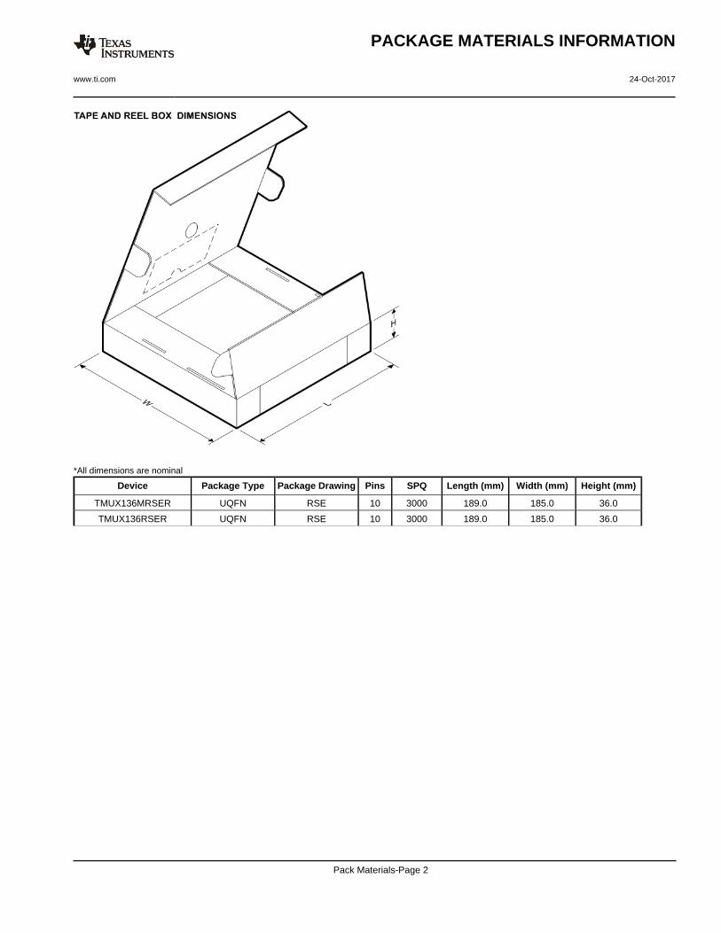
*All dimensions are nominal
Device Package Type Package Drawing Pins SPQ Length (mm) Width (mm) Height (mm)
TMUX136MRSER UQFN RSE 10 3000 189.0 185.0 36.0
TMUX136RSER UQFN RSE 10 3000 189.0 185.0 36.0
PACKAGE MATERIALS INFORMATION
www.ti.com 24-Oct-2017
Pack Materials-Page 2


IMPORTANT NOTICE
Texas Instruments Incorporated (TI) reserves the right to make corrections, enhancements, improvements and other changes to itssemiconductor products and services per JESD46, latest issue, and to discontinue any product or service per JESD48, latest issue. Buyersshould obtain the latest relevant information before placing orders and should verify that such information is current and complete.TI’s published terms of sale for semiconductor products (http://www.ti.com/sc/docs/stdterms.htm) apply to the sale of packaged integratedcircuit products that TI has qualified and released to market. Additional terms may apply to the use or sale of other types of TI products andservices.Reproduction of significant portions of TI information in TI data sheets is permissible only if reproduction is without alteration and isaccompanied by all associated warranties, conditions, limitations, and notices. TI is not responsible or liable for such reproduceddocumentation. Information of third parties may be subject to additional restrictions. Resale of TI products or services with statementsdifferent from or beyond the parameters stated by TI for that product or service voids all express and any implied warranties for theassociated TI product or service and is an unfair and deceptive business practice. TI is not responsible or liable for any such statements.Buyers and others who are developing systems that incorporate TI products (collectively, “Designers”) understand and agree that Designersremain responsible for using their independent analysis, evaluation and judgment in designing their applications and that Designers havefull and exclusive responsibility to assure the safety of Designers' applications and compliance of their applications (and of all TI productsused in or for Designers’ applications) with all applicable regulations, laws and other applicable requirements. Designer represents that, withrespect to their applications, Designer has all the necessary expertise to create and implement safeguards that (1) anticipate dangerousconsequences of failures, (2) monitor failures and their consequences, and (3) lessen the likelihood of failures that might cause harm andtake appropriate actions. Designer agrees that prior to using or distributing any applications that include TI products, Designer willthoroughly test such applications and the functionality of such TI products as used in such applications.TI’s provision of technical, application or other design advice, quality characterization, reliability data or other services or information,including, but not limited to, reference designs and materials relating to evaluation modules, (collectively, “TI Resources”) are intended toassist designers who are developing applications that incorporate TI products; by downloading, accessing or using TI Resources in anyway, Designer (individually or, if Designer is acting on behalf of a company, Designer’s company) agrees to use any particular TI Resourcesolely for this purpose and subject to the terms of this Notice.TI’s provision of TI Resources does not expand or otherwise alter TI’s applicable published warranties or warranty disclaimers for TIproducts, and no additional obligations or liabilities arise from TI providing such TI Resources. TI reserves the right to make corrections,enhancements, improvements and other changes to its TI Resources. TI has not conducted any testing other than that specificallydescribed in the published documentation for a particular TI Resource.Designer is authorized to use, copy and modify any individual TI Resource only in connection with the development of applications thatinclude the TI product(s) identified in such TI Resource. NO OTHER LICENSE, EXPRESS OR IMPLIED, BY ESTOPPEL OR OTHERWISETO ANY OTHER TI INTELLECTUAL PROPERTY RIGHT, AND NO LICENSE TO ANY TECHNOLOGY OR INTELLECTUAL PROPERTYRIGHT OF TI OR ANY THIRD PARTY IS GRANTED HEREIN, including but not limited to any patent right, copyright, mask work right, orother intellectual property right relating to any combination, machine, or process in which TI products or services are used. Informationregarding or referencing third-party products or services does not constitute a license to use such products or services, or a warranty orendorsement thereof. Use of TI Resources may require a license from a third party under the patents or other intellectual property of thethird party, or a license from TI under the patents or other intellectual property of TI.TI RESOURCES ARE PROVIDED “AS IS” AND WITH ALL FAULTS. TI DISCLAIMS ALL OTHER WARRANTIES ORREPRESENTATIONS, EXPRESS OR IMPLIED, REGARDING RESOURCES OR USE THEREOF, INCLUDING BUT NOT LIMITED TOACCURACY OR COMPLETENESS, TITLE, ANY EPIDEMIC FAILURE WARRANTY AND ANY IMPLIED WARRANTIES OFMERCHANTABILITY, FITNESS FOR A PARTICULAR PURPOSE, AND NON-INFRINGEMENT OF ANY THIRD PARTY INTELLECTUALPROPERTY RIGHTS. TI SHALL NOT BE LIABLE FOR AND SHALL NOT DEFEND OR INDEMNIFY DESIGNER AGAINST ANY CLAIM,INCLUDING BUT NOT LIMITED TO ANY INFRINGEMENT CLAIM THAT RELATES TO OR IS BASED ON ANY COMBINATION OFPRODUCTS EVEN IF DESCRIBED IN TI RESOURCES OR OTHERWISE. IN NO EVENT SHALL TI BE LIABLE FOR ANY ACTUAL,DIRECT, SPECIAL, COLLATERAL, INDIRECT, PUNITIVE, INCIDENTAL, CONSEQUENTIAL OR EXEMPLARY DAMAGES INCONNECTION WITH OR ARISING OUT OF TI RESOURCES OR USE THEREOF, AND REGARDLESS OF WHETHER TI HAS BEENADVISED OF THE POSSIBILITY OF SUCH DAMAGES.Unless TI has explicitly designated an individual product as meeting the requirements of a particular industry standard (e.g., ISO/TS 16949and ISO 26262), TI is not responsible for any failure to meet such industry standard requirements.Where TI specifically promotes products as facilitating functional safety or as compliant with industry functional safety standards, suchproducts are intended to help enable customers to design and create their own applications that meet applicable functional safety standardsand requirements. Using products in an application does not by itself establish any safety features in the application. Designers mustensure compliance with safety-related requirements and standards applicable to their applications. Designer may not use any TI products inlife-critical medical equipment unless authorized officers of the parties have executed a special contract specifically governing such use.Life-critical medical equipment is medical equipment where failure of such equipment would cause serious bodily injury or death (e.g., lifesupport, pacemakers, defibrillators, heart pumps, neurostimulators, and implantables). Such equipment includes, without limitation, allmedical devices identified by the U.S. Food and Drug Administration as Class III devices and equivalent classifications outside the U.S.TI may expressly designate certain products as completing a particular qualification (e.g., Q100, Military Grade, or Enhanced Product).Designers agree that it has the necessary expertise to select the product with the appropriate qualification designation for their applicationsand that proper product selection is at Designers’ own risk. Designers are solely responsible for compliance with all legal and regulatoryrequirements in connection with such selection.Designer will fully indemnify TI and its representatives against any damages, costs, losses, and/or liabilities arising out of Designer’s non-compliance with the terms and provisions of this Notice.
Mailing Address: Texas Instruments, Post Office Box 655303, Dallas, Texas 75265Copyright © 2017, Texas Instruments Incorporated