tms320c6748/46/42 & omap-l138 usb upstream … · 1 introduction application report...
TRANSCRIPT
1 Introduction
Application ReportSPRAB51–August 2009
TMS320C6748/46/42 and OMAP-L1x8 Universal Serial BusUpstream Device Compliance Testing
Christina Lam ......................................................................................................... DSPS Applications
ABSTRACTThis application report describes the TMS320C6748/46/42 and OMAP-L1x8 electricalcompliance of a high-speed (HS) universal serial bus (USB) operation conforming tothe USB 2.0 specification. The on-the-go (OTG) controller supports the USB 2.0 deviceand host mode at high-speed (HS), full-speed (FS) and low-speed (LS).
Contents1 Introduction .......................................................................................... 12 Test Items ........................................................................................... 23 Required Instruments .............................................................................. 34 Test Condition ...................................................................................... 45 References......................................................................................... 13
List of Figures
1 USB Functional Block Diagram ................................................................... 22 Eye Diagram/Signal Eye........................................................................... 53 Waveform Plot ...................................................................................... 64 Rise Time ............................................................................................ 65 Fall Time ............................................................................................. 66 Duty Cycle Distortion (DCD) ...................................................................... 77 Random Jitter/Deterministic Jitter/Total Jitter ................................................... 78 Setup Diagram for Performing HS Upstream Signal Quality Test ........................... 79 Setup Diagram for Performing HS Test_J/K/SE0_NAK Tests .............................. 1010 Setup Diagram for Performing Receiver Sensitivity Level Test ............................. 12
List of Tables
1 Device Electrical Tests Result Summary ........................................................ 22 Test Categories ..................................................................................... 33 Required Instruments .............................................................................. 34 Power Supply Voltage and Temperature Conditions .......................................... 45 Overall Result of the Signal Quality Test ........................................................ 56 Overall Results of 12-Bit SYNC Field .......................................................... 13
The device high-speed electrical test procedure is comprised of a series of tests and related proceduresdeveloped by the USB 2.0 compliance committee to verify electrical requirements of high-speed USBoperations designed to meet USB 2.0 specification. This document outlines the test setup and capturesthe results of the series tests performed on the C6748/46/42 and OMAP-L1x8 device.
All trademarks are the property of their respective owners.
SPRAB51–August 2009 TMS320C6748/46/42 and OMAP-L1x8 Universal Serial Bus Upstream Device Compliance Testing 1Submit Documentation Feedback

CPPIDMA
EngineFIFO
PacketEncode/Decode
USB2.0
PHYUSB
REFCLK(Optional)
Registers, Interrupts, Endpoint Control,and Packet Scheduling
InternalBus
2 Test Items
Test Items www.ti.com
The C6748/46/42 and OMAP-L1x8 device high-speed electrical test of the USB is performed on a VDB, aboard that is used to validate the device feature and is not optimized for USB characterization. Betterresults are expected when using test boards that are optimized for characterization purposes.
Figure 1 shows the USB functional block diagram.
Figure 1. USB Functional Block Diagram
Table 1 captures the series of compliance tests and the summary of results for each test. Details on thetests and specific results are discussed in the following sections.
Table 1. Device Electrical Tests Result SummaryTest# Test Items Result
USB_EL_2 HS Transmitter data rate 480 Mb/s ± 0.05% PASSUSB_EL_4 Signal quality test measured at the near end PASSUSB_EL_6 10% to 90% differential rise and fall time > 500ps PASSUSB_EL_7 Monotonic data transitions over the vertical openings in the appropriate EYE PASS
pattern templateUSB_EL_21 Synchronization (SYNC) field (packet originating from C6748/46/42 and PASS
OMAP-L1x8)USB_EL_22 Inter-packet gap (delay between Host and device packet) PASSUSB_EL_25 End of packet (EOP) field (packet originating from C6748/46/42 and OMAP-L1x8) PASSUSB_EL_28 Chirp reset time PASSUSB_EL_29 Chirp-K duration PASSUSB_EL_31 Delay between last Host chirp and device disconnect 1.5 K pull-up resistor and PASS
enable terminationUSB_EL_27 Chirp handshake generation while Host performing reset in the middle of idle PASS
(non-suspend HS mode)USB_EL_28 Chirp-K duration when reset is invoked from a suspended state PASSUSB_EL_38 Chirp reset time when reset is applied from a suspend state PASSUSB_EL_39 Device support for suspend state PASSUSB_EL_40 Device transitioning from suspend state to HS operation due to reaching the EOF PASSUSB_EL_8 Test J/K (controller transmits continuous J) PASSUSB_EL_8 Test K (controller transmits continuous K) PASSUSB_EL_9 Test_SE0_NAK (controller responds to any valid IN token with a NAK) PASSUSB_EL_16 Device receiver level PASSUSB_EL_17 Device squelch level PASSUSB_EL_18 Device capability for locking PLL with 12-bit SYNC field PASS
TMS320C6748/46/42 and OMAP-L1x8 Universal Serial Bus Upstream Device Compliance Testing2 SPRAB51–August 2009Submit Documentation Feedback

3 Required Instruments
www.ti.com Required Instruments
Table 2 lists the categorized series of tests outlined in the electrical test procedure in the USB2.0compliance test.
Table 2. Test CategoriesTest Items Categories
HS transmitter data rate 480 Mb/s ± 0.05% HS Upstream Signal Quality TestSignal quality test measured at the near end10% to 90% differential rise and fall time > 500 psMonotonic data transitions over the vertical openings in the appropriate EYE patterntemplateSYNC field (packet originating from C6748/46/42 and OMAP-L1x8) Device Packet ParametersInter-packet gap (delay between Host and device packet)EOP field (packet originating from C6748/46/42 and OMAP-L1x8)Chirp reset time Device Chirp TimingChirp-K durationDelay between the last Host chirp and the device disconnect 1.5 K pull-up resistor andenable terminationChirp handshake generation while Host is performing reset in the middle of idle Device Suspend/Resume/Reset Timing(non-suspend HS mode)Chirp-K duration when reset is invoked from a suspended stateChirp reset time when reset is applied from a suspended stateDevice support for suspend stateDevice transitioning from suspend state to high-speed operation when resume signaling isissued by the Host (from a suspend state)Test J (controller transmits continuous J) Device Test_J/K and Test_SE0_NAKTest K (controller transmits continuous K)Test_SE0_NAK (controller responds to any valid IN token with a NAK)Device receiver level Device Receiver SensitivityDevice squelch levelDevice capability for locking PLL with 12-bit SYNC Field
Table 3 lists the test instruments used to perform the outlined series of tests. These instruments are not allidentical to the ones outlined in the test document and are mentioned here since test setup, equipment,and cables have a large influence on the test outcome.
Table 3. Required InstrumentsType Manufacturer Product UseUSB high-speed electrical test tool to be USB-IF USBHSET To enumerate and send commandloaded on a test bed computerOscilloscope Tektronix DSA71604 To measure USB signalsDifferential probe (1) Tektronix P7313 Signal quality/receiver sensitivity testsSingle-ended FET probe (2) Tektronix P6243 Packet parameters/CHIRP timingsMeasurement application (USB test Tektronix TDSUSB USB compliance test softwaresoftware that is part of the scope specifically used for USBapplication)Test fixture Tektronix TDSUSBF For USB testPower supply Agilent E3633A 5 V power supply for TDSUSBFArbitrary waveform generator Tektronix AWG5002 To generate serial test data for
receiver sensitivity test
SPRAB51–August 2009 TMS320C6748/46/42 and OMAP-L1x8 Universal Serial Bus Upstream Device Compliance Testing 3Submit Documentation Feedback

4 Test Condition
4.1 Power Supply Voltage/Temperature
4.2 HS Upstream Signal Quality Test
4.2.1 EL_2: Signal Rate
4.2.2 EL_4: Signal Quality/Eye Diagram Test
4.2.3 EL_6: Rise and Fall Time
4.2.4 EL_7: Monotonic Data Transitions
Test Condition www.ti.com
Table 3. Required Instruments (continued)Type Manufacturer Product UseDigital multimeter Fluke Fluke 45 Series Measure voltage and current DP and
DM linesTest board (VDB) TI EVM Like Board Non-optimized test board used for
C6748/46/42 and OMAP-L1x8 Devicevalidation
Table 4 shows power supply voltage and temperature conditions.
Table 4. Power Supply Voltage and Temperature ConditionsParameter MIN TYP MAX UnitUSB_VDDA1P2LDO 1.14 1.2 1.26 VUSB_VDDA3P3 3.1 3.3 3.5 VOperating Temperature -10 25 95 °C
The HS upstream signal quality test uses the TEST_PACKET command to place the C6748/46/42 andOMAP-L1x8 device in test mode where the controller continuously transmits a fixed format test packet,which is defined in the USB 2.0 specification, Section 7.1.20. The test bed computer uses the electricaltest tools to issue the TEST_PACKET command to the C6748/46/42 and OMAP-L1x8. Upon receiving thiscommand, the C6748/46/42 and OMAP-L1x8 device enters the test packet test mode and beginscontinually sending a test packet. Using the test packet, this test measures the signal quality sent from theC6748/46/42 and OMAP-L1x8 device.
The oscilloscope, along the embedded software, automatically analyzes the test packet signal quality asobserved on the USB bus. For detailed procedures, see the Device High Speed Electrical Test Proceduredocument issued by the USB Implementers Forum (http://www.usb.org).
A USB 2.0 high-speed transmitter data rate must be 480 Mb/s ± 0.05%.
An eye diagram provides an intuitive view of jitter. It is a composite view of all the bit periods of a capturedwaveform superimposed upon each other. A USB 2.0 upstream port on a device, without a captive cable,must meet Template 1 transform waveform requirements measured at a test point close to the port.
A USB 2.0 high-speed driver must have 10% to 90% differential rise and fall times of greater than 500 ps.
A USB 2.0 driver must have monotonic data transitions over the vertical openings specified in theappropriate EYE pattern template.
TMS320C6748/46/42 and OMAP-L1x8 Universal Serial Bus Upstream Device Compliance Testing4 SPRAB51–August 2009Submit Documentation Feedback

www.ti.com Test Condition
Table 5. Overall Result of the Signal Quality TestStandard
Measurement Min. Max. Mean pk-pk Deviation RMS Pop. Status
Eye Diagram Test - - - - - - - PASS
465.5493 492.0319 4.488669 479.8074Signal Rate 480.0509 Mbps 0.0000 bps 512 PASSMbps Mbps Mbps Mbps
EOP Width - - 16.68762 ns - - - 1 PASS
EOP Width (Bits) - - 8.010908 - - - 1 PASS
814.3150 873.7150Falling Edge Rate 951.3559 V/µs 873.3275 V/µs 137.0409 V/µs 26.14228 V/µs 107 PASSV/µs V/µs
826.7541 896.8944Rising Edge Rate 967.2481 V/µs 896.4816 V/µs 140.4940 V/µs 27.33377 V/µs 108 PASSV/µs V/µs
Additional Information• Consecutive Jitter Range: -54.27 ps to 56.81 ps RMS Jitter 22.11 ps• KJ Paired Jitter Range: -60.14 ps to 56.99 ps RMS Jitter 22.89 ps• JK Paired Jitter Range: -57.15 ps to 76.99 ps RMS Jitter 21.13 ps
Figure 2. Eye Diagram/Signal Eye
SPRAB51–August 2009 TMS320C6748/46/42 and OMAP-L1x8 Universal Serial Bus Upstream Device Compliance Testing 5Submit Documentation Feedback

Rise Time10%
10%
Pattern
Fall Time10%
10%
Pattern
Test Condition www.ti.com
Figure 3. Waveform Plot
Figure 4. Rise Time
Figure 5. Fall Time
TMS320C6748/46/42 and OMAP-L1x8 Universal Serial Bus Upstream Device Compliance Testing6 SPRAB51–August 2009Submit Documentation Feedback

Pattern
Data RateDuty Cycle Distortion
Histogram
DJ
RJ RJ
TJ
RJ: Random jitter(Normal distribution / dependenton the Bit error rate)DJ: Deterministic jitter(Non-normal distribution)TJ: Total jitter ( = RJ + DJ )
USB CableC674x/
OMAP-L1xVDB
TestFixture
USB CableHost PC
(ElectricalTest Tools)
OscilloscopeDifferentialProbe
4.3 Device Packet Parameters
www.ti.com Test Condition
Figure 6. Duty Cycle Distortion (DCD)
Figure 7. Random Jitter/Deterministic Jitter/Total Jitter
Figure 8. Setup Diagram for Performing HS Upstream Signal Quality Test
Figure 8 is also used for other sets of tests:• Device Packet Parameters• Device CHIRP Timing• Device Suspend/Resume/Reset Timing
The device packet parameter tests are comprised of a set of tests related to fields pertaining to a USBtransfer. Unlike the signal quality test, the device does not need to enter into a test mode. Instead, the testbed computer invokes a set feature control transaction by pausing in between transfers. The single stepset feature command requires a setup stage and a status stage. The test bed computer invokes the setupstage transaction then pauses until told to continue. The packet delimiter fields, SYNC and EOP, aremeasured from the handshake packet during the setup stage in the transaction. The STEP button of theelectrical test tool is used to continue/finish the set feature command. The inter packet gap, the delaybetween the token packet originating from the Host and the data packet (zero length) originating from thedevice, is measured from the second half of the transfer.
The same setup file used for the signal quality testing is used to perform device packet parameters tests.Three device parameters are tested from this setup: SYNC, EOP, and inter-packet-gap
SPRAB51–August 2009 TMS320C6748/46/42 and OMAP-L1x8 Universal Serial Bus Upstream Device Compliance Testing 7Submit Documentation Feedback
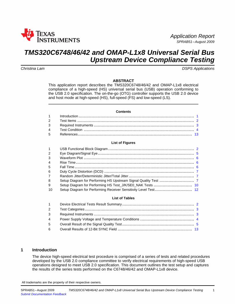
4.3.1 EL_21: SYNC (Synchronization) Field
4.3.2 EL_22: Inter-Packet-Gap Field
4.3.3 EL_25: EOP (End-of-Packet) Field
4.4 Device CHIRP Timing
Test Condition www.ti.com
The SYNC field for all transmitted packets (not repeated packets) must begin with a 32-bit SYNC field.
Handshake packet SYNC field: PASS
Note: Measured value: 66.91 ns => 66.91 ns x 480 Mbps = 32.1168 bits
When transmitting after receiving a packet, hosts and devices must provide an inter-packet-gap of at least8 bit times and not more than 192 bit times.
Packet gap between Host token packet and device data packet: PASS
Note: Measured value: 240.24 ns => 240.24 ns x 480 Mbps = 115.3152 bits
The EOP for all transmitted packets (except state of finish (SOF)) must be an 8-bit non-return to zeroinverted (NRZI) byte without bit stuffing.
Handshake packet EOP field: PASS.
Note: Measured value: 16.58 ns => 16.58 ns x 480 Mbps = 7.9584 bits
The device chirp timing is used to validate a high-speed detection handshake and occurs during the timeof reset. Some time after the Host resets a high-speed device, the device should indicate its high-speedcapability by generating a chirp-K signal. The Host will follow up by generating three sets of chirp-KJsignals in a full-speed signaling environment. The device should disconnect its 1.5KΩ pull-up resistor andenable the 45 Ω termination resistors right after the last chirp-J from the Host.
You can invoke this test using the same setup as the signal quality testing shown in Figure 8, with the twoprobes replacing the differential probe; however, in this case use the Host test bed computer to enumeratethe C6748/46/42 and OMAP-L1x8 device only. You can also invoke the Enumerate Bus single-ended fromthe high-speed electrical test tool to perform the same test.
Note: Make sure your scope is configured and ready for capturing/triggering the enumerationprocess. Start by disconnecting the USB cable connection between the Host and USB fixture(TDSUSB2F). Have the device side code ready and running. When connecting the USBcable from the Host onto the USB test fixture, the enumeration process takes place and iscaptured on the scope.
Figure 8 displays the setup used for performing these set of tests.
Note: In place of the differential probe, two single-ended FET probes are used.
8 TMS320C6748/46/42 and OMAP-L1x8 Universal Serial Bus Upstream Device Compliance Testing SPRAB51–August 2009Submit Documentation Feedback

4.4.1 EL_28: CHIRP Reset Time
4.4.2 EL_29: CHIRP-K Duration
4.4.3 EL_31: 1.5 K Pull-Up Resistor Disconnection
4.5 Device Suspend/Resume/Reset Timing
4.5.1 EL_27: CHIRP Handshake Generation From Non-Suspended State
4.5.2 EL_28: CHIRP-K Duration From a Suspended State
www.ti.com Test Condition
Devices must transmit a chirp handshake no sooner than 2.5 µs and no later than 3 ms when being resetfrom suspend or a full-speed state.
CHIRP reset time: PASS
Note: Measured value: 5.903741 µs
The chirp handshake generated by a device must be at least 1ms and not more than 7 ms in duration.
CHIRP-K duration: PASS
Note: Measured value: 1.096818 ms
When a device detects a valid set of chirp-KJ sequences during device speed detection, the device mustdisconnect its 1.5 K pull-up resistor and enable its high-speed terminations within 500 µs.
1.5K pull-up resistor disconnect: PASS
Note: Measured value: 7 µs
A device must support suspend state. It is supposed to go through a suspend state when it is forced to goto suspend state by the host or when there is no activity for ≥ 3 ms. A high-speed device indicates itshigh-speed operation capability when the Host invokes a reset on the device by generating a chirp-Ksequence signal.
Figure 8 displays the setup used for performing these set of tests with the two single-ended probesreplacing the differential probe.
A device must transmit a chirp handshake no sooner than 3.1 ms and no later than 6 ms when being resetfrom a non-suspended high-speed mode. The timing is measured from the beginning of the last SOFtransmitted and before the reset begins.
Chirp handshake generation when reset from a non-suspended state: PASS
Note: Measured value: 3.102598 ms
A device must transmit a chirp handshake (chirp-K) no sooner than 2.5 µs and no later than 3 ms whenbeing reset from suspend or a full-speed mode.
Chirp-K duration from a suspend state: PASS
Note: Measured value: 5.592141 µs
SPRAB51–August 2009 TMS320C6748/46/42 and OMAP-L1x8 Universal Serial Bus Upstream Device Compliance Testing 9Submit Documentation Feedback

4.5.3 EL_38: CHIRP Reset Time From a Suspended State
4.5.4 EL_39: Device Support for Suspend State
4.5.5 EL_40: Device Resuming With High-Speed Operation After Resume Signaling From a Suspend
4.6 Device Test_J/K/SE0_NAK
USB CableC674x/
OMAP-L1xVDB
TestFixture
USB CableHost PC
(ElectricalTest Tools)
OscilloscopeTwoSingle EndedFET Probes
DM
Test Condition www.ti.com
A device must revert to full-speed termination no later than 125 µs after there is a 3 ms idle period on thebus.
Chirp reset time when reset is applied from a suspended state. PASS
Note: Measured value: 3.0036 ms
A device must support suspend state. The device should go into suspend state when forced by the Host.
Device support for suspend state: PASS
Note: No value to measure. Make sure SOF is not present.
StateA device must transition its operating to a high-speed operation after receiving the resume signal. This iswith the assumption that the device was operating at high-speed prior to being suspended.
Device resumes to HS operation at the end of resume signaling: PASS
Note: No value to measure. SOF at a HS signal level is observed.
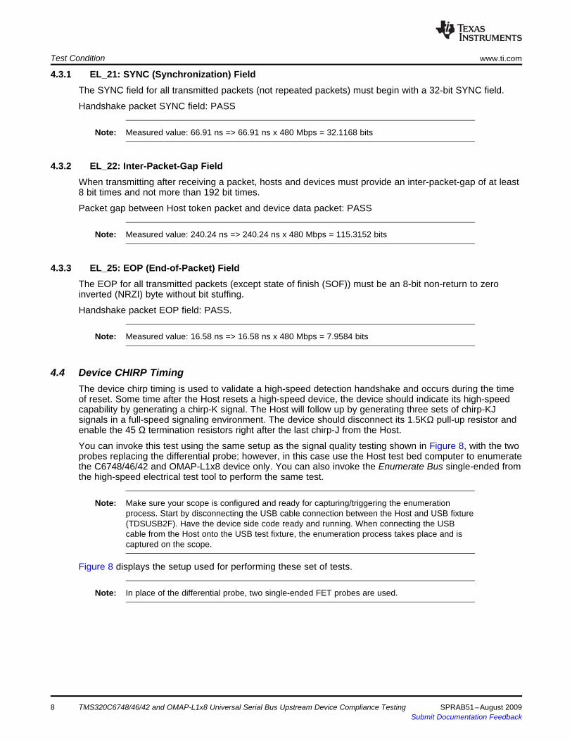
A USB controller that is USB 2.0 specification compliant requires that the controller support four tests:Test_SE0_NAK, Test_J, Test_K, and Test_Packet. A digital Multimeter is used for the DC voltage level ofD+ and D- data lines.
Test_SE0_NAK places the controller to remain in high-speed mode but respond to any valid IN token witha NAK. Test_J places the controller to transmit a continuous J on the bus. Test_K places the controller totransmit a continuous K on the bus.
Figure 9 displays the setup used for performing the tests mentioned in Section 4.6.
Figure 9. Setup Diagram for Performing HS Test_J/K/SE0_NAK Tests
10 TMS320C6748/46/42 and OMAP-L1x8 Universal Serial Bus Upstream Device Compliance Testing SPRAB51–August 2009Submit Documentation Feedback
4.6.1 EL_8: Test_J
4.6.2 EL_8: Test_K
4.6.3 EL_9: Test_SE0_NAK
www.ti.com Test Condition
When the D+ is driven high, the output voltage must be 400 mV ± 10% when terminated with precision 45Ω resistor.
D+ data line DC voltage level: PASS
Note: Measured value: 0.391 V
D- data line DC voltage level: PASS
Note: Measured value: 0.002 V
When the D- is driven high, the output voltage must be 400 mV ± 10% when terminated with precision 45Ω resistor.
D- data line DC voltage level: PASS
Note: Measured value: 0.388 V
D+ data line DC voltage level: PASS
Note: Measured value: 0.002 V
When either D+ and D- are not being driven, the output voltage must be 0 V ± 10% when terminated withprecision 45 Ω resistors to ground.
D+ data line DC voltage level: PASS
Note: Measured value: 0.001 V
D- data line DC voltage level: PASS
Note: Measured value: 0.001 V
SPRAB51–August 2009 TMS320C6748/46/42 and OMAP-L1x8 Universal Serial Bus Upstream Device Compliance Testing 11Submit Documentation Feedback
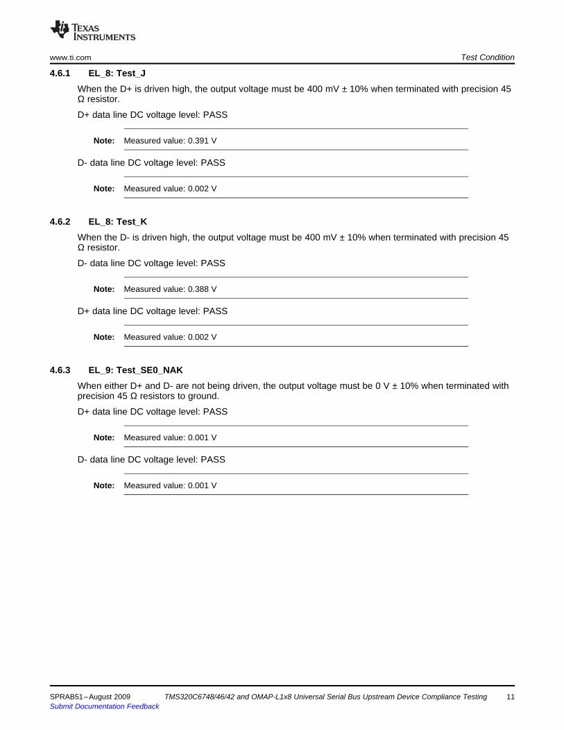
4.7 Receiver Sensitivity Level
USB CableC674x/
OMAP-L1xVDB
TestFixture
USB CableHost PC
(ElectricalTest Tools)
OscilloscopeDifferential
Probe
Arbitrary WaveformGenerator (AWG5002)SMA
Cable
4.7.1 EL_16: Squelch Level.
4.7.2 EL_17: Receiver Level
Test Condition www.ti.com
The HS receiver sensitivity and squelch test uses the TEST_SE0_NAK command. The electrical test toolinvokes the TEST_SE0_NAK command from the test bed computer to the C6748/46/42 and OMAP-L1x8.Upon receiving this command from the host, the C6748/46/42 and OMAP-L1x8 device enters into a testmode where it continually responds with a NAK upon receiving an IN token.
Once the test setup is done by the host on the test bed computer, the arbitrary waveform replaces thehost generating an IN token waveform which forces the device to respond with a NAK. The test fixture hasa switch that establishes a link between the device and the Host or the device and the arbitrary waveformgenerator.
Two waveforms, one with a 32-bit SYNC field and another with a 12-bit SYNC field are used inconstructing the IN token to be sent to the device. The waveform with 32-bit SYNC field is used for thereceiver and squelch test. The 12-bit field is used for testing device capability on detecting the datatransmission.
Figure 10 displays the setup used for performing a receiver sensitivity level test.
Figure 10. Setup Diagram for Performing Receiver Sensitivity Level Test
A high-speed capable device must implement a transmission envelope detector that indicates squelch(i.e., never receives packet) when a receiver’s input falls below 100 mV differential amplitude.
A high-speed capable device must implement a transmission envelope detector that does not indicatesquelch (i.e., reliably receives packets) when a receiver exceeds 150 mV differential amplitude.
12 TMS320C6748/46/42 and OMAP-L1x8 Universal Serial Bus Upstream Device Compliance Testing SPRAB51–August 2009Submit Documentation Feedback

4.7.3 EL_18: 12-Bit SYNC Field
4.8 USB Checklist
5 References
www.ti.com References
The SYNC pattern used for high-speed transmission is required to be 15 KJ pairs followed by 2 K’s, for atotal of 32 symbols. Hubs are allowed to drop up to 4 bits from the start of the SYNC pattern whenrepeating packets; however, hubs must not corrupt any repeated bits of the SYNC field. Therefore, afterbeing repeated by five hubs, a packet’s SYNC field may be as short as 12 bits. The device attached to thefifth hub should be able to detect the SYNC.
Table 6. Overall Results of 12-Bit SYNC FieldMeasurementName Positive Peak Negative Peak USB Limits StatusReceiver Level 136 mV 144 mV Must receive ≤ 150 mV Must receive ≤ 200 mV PASSSquelch Level 132 mV 136 mV Must not respond < 100 Must not respond < 50 PASS
mV mVEL_18 Level - - Device should respond - PASS
with minimum 12 bitSYNC field
A standard USB checklist from the USB Implementers Forum has been populated with informationpertaining to the C6748/46/42 and OMAP-L1x8 devices. For more information, see the TMS320DM64xxUSB Compliance Checklist (SPRAAT5).
• Device High Speed Electrical Test Procedure - USB Implementers Forum (http://www.usb.org)• TMS320DM64xx USB Compliance Checklist (SPRAAT5)
SPRAB51–August 2009 TMS320C6748/46/42 and OMAP-L1x8 Universal Serial Bus Upstream Device Compliance Testing 13Submit Documentation Feedback
IMPORTANT NOTICETexas Instruments Incorporated and its subsidiaries (TI) reserve the right to make corrections, modifications, enhancements, improvements,and other changes to its products and services at any time and to discontinue any product or service without notice. Customers shouldobtain the latest relevant information before placing orders and should verify that such information is current and complete. All products aresold subject to TI’s terms and conditions of sale supplied at the time of order acknowledgment.TI warrants performance of its hardware products to the specifications applicable at the time of sale in accordance with TI’s standardwarranty. Testing and other quality control techniques are used to the extent TI deems necessary to support this warranty. Except wheremandated by government requirements, testing of all parameters of each product is not necessarily performed.TI assumes no liability for applications assistance or customer product design. Customers are responsible for their products andapplications using TI components. To minimize the risks associated with customer products and applications, customers should provideadequate design and operating safeguards.TI does not warrant or represent that any license, either express or implied, is granted under any TI patent right, copyright, mask work right,or other TI intellectual property right relating to any combination, machine, or process in which TI products or services are used. Informationpublished by TI regarding third-party products or services does not constitute a license from TI to use such products or services or awarranty or endorsement thereof. Use of such information may require a license from a third party under the patents or other intellectualproperty of the third party, or a license from TI under the patents or other intellectual property of TI.Reproduction of TI information in TI data books or data sheets is permissible only if reproduction is without alteration and is accompaniedby all associated warranties, conditions, limitations, and notices. Reproduction of this information with alteration is an unfair and deceptivebusiness practice. TI is not responsible or liable for such altered documentation. Information of third parties may be subject to additionalrestrictions.Resale of TI products or services with statements different from or beyond the parameters stated by TI for that product or service voids allexpress and any implied warranties for the associated TI product or service and is an unfair and deceptive business practice. TI is notresponsible or liable for any such statements.TI products are not authorized for use in safety-critical applications (such as life support) where a failure of the TI product would reasonablybe expected to cause severe personal injury or death, unless officers of the parties have executed an agreement specifically governingsuch use. Buyers represent that they have all necessary expertise in the safety and regulatory ramifications of their applications, andacknowledge and agree that they are solely responsible for all legal, regulatory and safety-related requirements concerning their productsand any use of TI products in such safety-critical applications, notwithstanding any applications-related information or support that may beprovided by TI. Further, Buyers must fully indemnify TI and its representatives against any damages arising out of the use of TI products insuch safety-critical applications.TI products are neither designed nor intended for use in military/aerospace applications or environments unless the TI products arespecifically designated by TI as military-grade or "enhanced plastic." Only products designated by TI as military-grade meet militaryspecifications. Buyers acknowledge and agree that any such use of TI products which TI has not designated as military-grade is solely atthe Buyer's risk, and that they are solely responsible for compliance with all legal and regulatory requirements in connection with such use.TI products are neither designed nor intended for use in automotive applications or environments unless the specific TI products aredesignated by TI as compliant with ISO/TS 16949 requirements. Buyers acknowledge and agree that, if they use any non-designatedproducts in automotive applications, TI will not be responsible for any failure to meet such requirements.Following are URLs where you can obtain information on other Texas Instruments products and application solutions:Products ApplicationsAmplifiers amplifier.ti.com Audio www.ti.com/audioData Converters dataconverter.ti.com Automotive www.ti.com/automotiveDLP® Products www.dlp.com Broadband www.ti.com/broadbandDSP dsp.ti.com Digital Control www.ti.com/digitalcontrolClocks and Timers www.ti.com/clocks Medical www.ti.com/medicalInterface interface.ti.com Military www.ti.com/militaryLogic logic.ti.com Optical Networking www.ti.com/opticalnetworkPower Mgmt power.ti.com Security www.ti.com/securityMicrocontrollers microcontroller.ti.com Telephony www.ti.com/telephonyRFID www.ti-rfid.com Video & Imaging www.ti.com/videoRF/IF and ZigBee® Solutions www.ti.com/lprf Wireless www.ti.com/wireless
Mailing Address: Texas Instruments, Post Office Box 655303, Dallas, Texas 75265Copyright © 2009, Texas Instruments Incorporated