tms320c6000 dsp general-purpose input/output (gpio) reference … · tms320c6000 dsp...
TRANSCRIPT
TMS320C6000 DSPGeneral-Purpose Input/Output (GPIO)
Reference Guide
Literature Number: SPRU584AMarch 2004
IMPORTANT NOTICE
Texas Instruments Incorporated and its subsidiaries (TI) reserve the right to make corrections, modifications,enhancements, improvements, and other changes to its products and services at any time and to discontinueany product or service without notice. Customers should obtain the latest relevant information before placingorders and should verify that such information is current and complete. All products are sold subject to TI’s termsand conditions of sale supplied at the time of order acknowledgment.
TI warrants performance of its hardware products to the specifications applicable at the time of sale inaccordance with TI’s standard warranty. Testing and other quality control techniques are used to the extent TIdeems necessary to support this warranty. Except where mandated by government requirements, testing of allparameters of each product is not necessarily performed.
TI assumes no liability for applications assistance or customer product design. Customers are responsible fortheir products and applications using TI components. To minimize the risks associated with customer productsand applications, customers should provide adequate design and operating safeguards.
TI does not warrant or represent that any license, either express or implied, is granted under any TI patent right,copyright, mask work right, or other TI intellectual property right relating to any combination, machine, or processin which TI products or services are used. Information published by TI regarding third-party products or servicesdoes not constitute a license from TI to use such products or services or a warranty or endorsement thereof.Use of such information may require a license from a third party under the patents or other intellectual propertyof the third party, or a license from TI under the patents or other intellectual property of TI.
Reproduction of information in TI data books or data sheets is permissible only if reproduction is withoutalteration and is accompanied by all associated warranties, conditions, limitations, and notices. Reproductionof this information with alteration is an unfair and deceptive business practice. TI is not responsible or liable forsuch altered documentation.
Resale of TI products or services with statements different from or beyond the parameters stated by TI for thatproduct or service voids all express and any implied warranties for the associated TI product or service andis an unfair and deceptive business practice. TI is not responsible or liable for any such statements.
Following are URLs where you can obtain information on other Texas Instruments products and applicationsolutions:
Products Applications
Amplifiers amplifier.ti.com Audio www.ti.com/audio
Data Converters dataconverter.ti.com Automotive www.ti.com/automotive
DSP dsp.ti.com Broadband www.ti.com/broadband
Interface interface.ti.com Digital Control www.ti.com/digitalcontrol
Logic logic.ti.com Military www.ti.com/military
Power Mgmt power.ti.com Optical Networking www.ti.com/opticalnetwork
Microcontrollers microcontroller.ti.com Security www.ti.com/security
Telephony www.ti.com/telephony
Video & Imaging www.ti.com/video
Wireless www.ti.com/wireless
Mailing Address: Texas Instruments
Post Office Box 655303 Dallas, Texas 75265
Copyright 2004, Texas Instruments Incorporated

3General-Purpose Input/Output (GPIO)SPRU584A
Preface
Read This First
About This Manual
This document describes the general-purpose input/output (GPIO) peripheralin the digital signal processors (DSPs) of the TMS320C6000 DSP family.
Notational Conventions
This document uses the following conventions.
� Hexadecimal numbers are shown with the suffix h. For example, thefollowing number is 40 hexadecimal (decimal 64): 40h.
� When referencing specific register bits, the X in the register bit name isreplaced with the bit number; for example, GPXDIR refers to the bit fieldof the GPIO direction register and GP15DIR refers to bit 15 of GPDIR.
� Registers in this document are shown in figures and described in tables.
� Each register figure shows a rectangle divided into fields that representthe fields of the register. Each field is labeled with its bit name, itsbeginning and ending bit numbers above, and its read/write propertiesbelow. A legend explains the notation used for the properties.
� Reserved bits in a register figure designate a bit that is used for futuredevice expansion.
Related Documentation From Texas Instruments
The following documents describe the C6000 devices and related supporttools. Copies of these documents are available on the Internet at www.ti.com.Tip: Enter the literature number in the search box provided at www.ti.com.
TMS320C6000 CPU and Instruction Set Reference Guide (literaturenumber SPRU189) describes the TMS320C6000 CPU architecture,instruction set, pipeline, and interrupts for these digital signal processors.
TMS320C6000 DSP Peripherals Overview Reference Guide (literaturenumber SPRU190) describes the peripherals available on theTMS320C6000 DSPs.

Trademarks
4 General-Purpose Input/Output (GPIO) SPRU584A
TMS320C6000 Technical Brief (literature number SPRU197) gives anintroduction to the TMS320C62x and TMS320C67x DSPs, develop-ment tools, and third-party support.
TMS320C64x Technical Overview (SPRU395) gives an introduction to theTMS320C64x DSP and discusses the application areas that areenhanced by the TMS320C64x VelociTI.
TMS320C6000 Programmer’s Guide (literature number SPRU198)describes ways to optimize C and assembly code for theTMS320C6000 DSPs and includes application program examples.
TMS320C6000 Code Composer Studio Tutorial (literature numberSPRU301) introduces the Code Composer Studio integrated develop-ment environment and software tools.
Code Composer Studio Application Programming Interface ReferenceGuide (literature number SPRU321) describes the Code ComposerStudio application programming interface (API), which allows you toprogram custom plug-ins for Code Composer.
TMS320C6x Peripheral Support Library Programmer’s Reference(literature number SPRU273) describes the contents of theTMS320C6000 peripheral support library of functions and macros. Itlists functions and macros both by header file and alphabetically,provides a complete description of each, and gives code examples toshow how they are used.
TMS320C6000 Chip Support Library API Reference Guide (literaturenumber SPRU401) describes a set of application programming interfaces(APIs) used to configure and control the on-chip peripherals.
Trademarks
Code Composer Studio, C6000, C62x, C64x, C67x, TMS320C6000,TMS320C62x, TMS320C64x, TMS320C67x, and VelociTI are trademarks ofTexas Instruments.
Related Documentation From Texas Instruments / Trademarks
Contents
5General-Purpose Input/Output (GPIO)SPRU584A
Contents
1 Overview 9. . . . . . . . . . . . . . . . . . . . . . . . . . . . . . . . . . . . . . . . . . . . . . . . . . . . . . . . . . . . . . . . . . . . . . . . . .
2 GPIO Function 11. . . . . . . . . . . . . . . . . . . . . . . . . . . . . . . . . . . . . . . . . . . . . . . . . . . . . . . . . . . . . . . . . . .
3 Interrupt and Event Generation 13. . . . . . . . . . . . . . . . . . . . . . . . . . . . . . . . . . . . . . . . . . . . . . . . . . . . 3.1 Pass-Through Mode 14. . . . . . . . . . . . . . . . . . . . . . . . . . . . . . . . . . . . . . . . . . . . . . . . . . . . . . . . . 3.2 Logic Mode 15. . . . . . . . . . . . . . . . . . . . . . . . . . . . . . . . . . . . . . . . . . . . . . . . . . . . . . . . . . . . . . . . .
3.2.1 Delta OR Mode (GPINTDV = 0, LOGIC = 0) 18. . . . . . . . . . . . . . . . . . . . . . . . . . . . . 3.2.2 Delta AND Mode (GPINTDV = 0, LOGIC = 1) 20. . . . . . . . . . . . . . . . . . . . . . . . . . . . 3.2.3 Value AND Mode (GPINTDV = 1, LOGIC = 1) 23. . . . . . . . . . . . . . . . . . . . . . . . . . . .
3.3 GPINT Muxing With GP0 and/or GPINT0 25. . . . . . . . . . . . . . . . . . . . . . . . . . . . . . . . . . . . . . .
4 Interrupts and Events 26. . . . . . . . . . . . . . . . . . . . . . . . . . . . . . . . . . . . . . . . . . . . . . . . . . . . . . . . . . . . .
5 Registers 27. . . . . . . . . . . . . . . . . . . . . . . . . . . . . . . . . . . . . . . . . . . . . . . . . . . . . . . . . . . . . . . . . . . . . . . . 5.1 GPIO Enable Register (GPEN) 27. . . . . . . . . . . . . . . . . . . . . . . . . . . . . . . . . . . . . . . . . . . . . . . . 5.2 GPIO Direction Register (GPDIR) 29. . . . . . . . . . . . . . . . . . . . . . . . . . . . . . . . . . . . . . . . . . . . . . 5.3 GPIO Value Register (GPVAL) 30. . . . . . . . . . . . . . . . . . . . . . . . . . . . . . . . . . . . . . . . . . . . . . . . 5.4 GPIO Delta High Register (GPDH) 31. . . . . . . . . . . . . . . . . . . . . . . . . . . . . . . . . . . . . . . . . . . . . 5.5 GPIO Delta Low Register (GPDL) 32. . . . . . . . . . . . . . . . . . . . . . . . . . . . . . . . . . . . . . . . . . . . . . 5.6 GPIO High Mask Register (GPHM) 33. . . . . . . . . . . . . . . . . . . . . . . . . . . . . . . . . . . . . . . . . . . . 5.7 GPIO Low Mask Register (GPLM) 34. . . . . . . . . . . . . . . . . . . . . . . . . . . . . . . . . . . . . . . . . . . . . 5.8 GPIO Global Control Register (GPGC) 35. . . . . . . . . . . . . . . . . . . . . . . . . . . . . . . . . . . . . . . . . 5.9 GPIO Interrupt Polarity Register (GPPOL) 37. . . . . . . . . . . . . . . . . . . . . . . . . . . . . . . . . . . . . .
Revision History 39. . . . . . . . . . . . . . . . . . . . . . . . . . . . . . . . . . . . . . . . . . . . . . . . . . . . . . . . . . . . . . . . . . . . .
Figures
6 General-Purpose Input/Output (GPIO) SPRU584A
Figures
1 TMS320C64x DSP Block Diagram 9. . . . . . . . . . . . . . . . . . . . . . . . . . . . . . . . . . . . . . . . . . . . . . . . 2 GPIO Peripheral Block Diagram 10. . . . . . . . . . . . . . . . . . . . . . . . . . . . . . . . . . . . . . . . . . . . . . . . . . 3 GPIO Functional Block Diagram 12. . . . . . . . . . . . . . . . . . . . . . . . . . . . . . . . . . . . . . . . . . . . . . . . . 4 GPIO Interrupt and Event Generation Block Diagram 13. . . . . . . . . . . . . . . . . . . . . . . . . . . . . . . 5 GPINTn Generation in Pass-Through Mode 15. . . . . . . . . . . . . . . . . . . . . . . . . . . . . . . . . . . . . . . 6 GPINT Generation in Logic Mode 16. . . . . . . . . . . . . . . . . . . . . . . . . . . . . . . . . . . . . . . . . . . . . . . . 7 GPINT Generation in Delta OR Mode 18. . . . . . . . . . . . . . . . . . . . . . . . . . . . . . . . . . . . . . . . . . . . . 8 GPINT Generation in Delta AND Mode 21. . . . . . . . . . . . . . . . . . . . . . . . . . . . . . . . . . . . . . . . . . . . 9 GPINT Generation in Value AND Mode 23. . . . . . . . . . . . . . . . . . . . . . . . . . . . . . . . . . . . . . . . . . . 10 GPINT Connection to GP0 and GPINT0 25. . . . . . . . . . . . . . . . . . . . . . . . . . . . . . . . . . . . . . . . . . . 11 GPIO Enable Register (GPEN) 28. . . . . . . . . . . . . . . . . . . . . . . . . . . . . . . . . . . . . . . . . . . . . . . . . . 12 GPIO Direction Register (GPDIR) 29. . . . . . . . . . . . . . . . . . . . . . . . . . . . . . . . . . . . . . . . . . . . . . . . 13 GPIO Value Register (GPVAL) 30. . . . . . . . . . . . . . . . . . . . . . . . . . . . . . . . . . . . . . . . . . . . . . . . . . . 14 GPIO Delta High Register (GPDH) 31. . . . . . . . . . . . . . . . . . . . . . . . . . . . . . . . . . . . . . . . . . . . . . . 15 GPIO Delta Low Register (GPDL) 32. . . . . . . . . . . . . . . . . . . . . . . . . . . . . . . . . . . . . . . . . . . . . . . . 16 GPIO High Mask Register (GPHM) 33. . . . . . . . . . . . . . . . . . . . . . . . . . . . . . . . . . . . . . . . . . . . . . . 17 GPIO Low Mask Register (GPLM) 34. . . . . . . . . . . . . . . . . . . . . . . . . . . . . . . . . . . . . . . . . . . . . . . . 18 GPIO Global Control Register (GPGC) 35. . . . . . . . . . . . . . . . . . . . . . . . . . . . . . . . . . . . . . . . . . . . 19 GPIO Interrupt Polarity Register (GPPOL) 37. . . . . . . . . . . . . . . . . . . . . . . . . . . . . . . . . . . . . . . . .

Tables
7General-Purpose Input/Output (GPIO)SPRU584A
Tables
1 Logic Mode Truth Table 17. . . . . . . . . . . . . . . . . . . . . . . . . . . . . . . . . . . . . . . . . . . . . . . . . . . . . . . . . 2 GPIO Interrupts to CPU and Events to EDMA 26. . . . . . . . . . . . . . . . . . . . . . . . . . . . . . . . . . . . . . 3 GPIO Registers 27. . . . . . . . . . . . . . . . . . . . . . . . . . . . . . . . . . . . . . . . . . . . . . . . . . . . . . . . . . . . . . . . 4 GPIO Enable Register (GPEN) Field Descriptions 28. . . . . . . . . . . . . . . . . . . . . . . . . . . . . . . . . . 5 GPIO Direction Register (GPDIR) Field Descriptions 29. . . . . . . . . . . . . . . . . . . . . . . . . . . . . . . . 6 GPIO Value Register (GPVAL) Field Descriptions 30. . . . . . . . . . . . . . . . . . . . . . . . . . . . . . . . . . 7 GPIO Delta High Register (GPDH) Field Descriptions 31. . . . . . . . . . . . . . . . . . . . . . . . . . . . . . . 8 GPIO Delta Low Register (GPDL) Field Descriptions 32. . . . . . . . . . . . . . . . . . . . . . . . . . . . . . . . 9 GPIO High Mask Register (GPHM) Field Descriptions 33. . . . . . . . . . . . . . . . . . . . . . . . . . . . . . 10 GPIO Low Mask Register (GPLM) Field Descriptions 34. . . . . . . . . . . . . . . . . . . . . . . . . . . . . . . 11 GPIO Global Control Register (GPGC) Field Descriptions 35. . . . . . . . . . . . . . . . . . . . . . . . . . . 12 GPIO Interrupt Polarity Register (GPPOL) Field Descriptions 37. . . . . . . . . . . . . . . . . . . . . . . . 13 Document Revision History 39. . . . . . . . . . . . . . . . . . . . . . . . . . . . . . . . . . . . . . . . . . . . . . . . . . . . . .

8 General-Purpose Input/Output (GPIO) SPRU584A
This page is intentionally left blank.

9General-Purpose Input/Output (GPIO)SPRU584A
General-Purpose Input/Output (GPIO)
This document describes the general-purpose input/output (GPIO) peripheralin the digital signal processors (DSPs) of the TMS320C6000 DSP family.
1 Overview
The general-purpose input/output (GPIO) peripheral provides dedicatedgeneral-purpose pins that can be configured as either inputs or outputs. Whenconfigured as an output, you can write to an internal register to control the statedriven on the output pin. When configured as an input, you can detect the stateof the input by reading the state of an internal register.
In addition, the GPIO peripheral can produce CPU interrupts and EDMAevents in different interrupt/event generation modes.
Figure 1 shows the GPIO peripheral in the TMS320C64x DSP. Figure 2shows the GPIO peripheral block diagram.
Figure 1. TMS320C64x DSP Block Diagram
C6000 DSP coreInstruction Fetch
Instruction Dispatch
Instruction Decode
Data Path A
A Register File
L1 S1 M1 D1
ControlRegisters
ControlLogic
Test
In−CircuitEmulation
InterruptControl
Data Path B
B Register File
L2S2M2D2
L1P Cache
L2Memory
L1D Cache
EnhancedDMA
Controller
Power DownLogic
EMIF
OtherPeripherals
BootConfiguration
InterruptSelector
PLL
GPIO

Overview
General-Purpose Input/Output (GPIO)10 SPRU584A
Some GPIO pins are MUXed with other device pins. On a given device, all bitsmay not be implemented for each GPIO register. Refer to the device-specificdatasheet for details on specific MUXing and for the availability of the registerbits. GPINT[0−15] are all synchronization events to the EDMA. However, onlyGPINT0 and GPINT[4−7] are available as interrupt sources to the CPU.
Figure 2. GPIO Peripheral Block Diagram
GP0
GP1
GP2
GP3
GP4
GP5
GP6
GP7
GP8
GP9
GP10
GP11
GP12
GP13
GP14
GP15
GPINT0
GPINT4
GPINT5
GPINT6
GPINT7
Controlregisters
Interrupts to CPUand synchronization
events to EDMA�
Internalperipheral bus
GPIO
GPINT3
GPINT1
GPINT2
GPINT8
GPINT9
GPINT10
GPINT11
GPINT12
GPINT13
GPINT14
GPINT15
� Some of the GPn pins are MUXed with other device signals. The number of available GPn pins is device specific. Refer to thedevice-specific datasheet for details.
� All GPINTn are synchronization events to the EDMA. Only GPINT0 and GPINT[4−7] are available as interrupts to the CPU.

GPIO Function
11General-Purpose Input/Output (GPIO)SPRU584A
2 GPIO Function
A GPIO pin can operate as a general-purpose input/output once it is enabledin the GPIO enable register (GPEN). You can independently configure eachGPIO pin as either an input or an output using the GPIO direction register(GPDIR). When configured as an output (GPXDIR bit = 1), the value in theGPXVAL bit in the GPIO value register (GPVAL) is driven on the correspondingGPn pin. When configured as an input (GPXDIR bit = 0), the state of the inputcan be read from the corresponding GPXVAL bit. Refer to section 5 for detailson the GPIO registers.
In addition to the general-purpose input/output function, the edge-detect logicin the GPIO peripheral reflects whether a transition has occurred on a givenGPIO signal that is configured as an input (GPXDIR bit = 0). The GPIO signaltransition is reflected in the GPIO delta registers (GPDH or GPDL). TheGPXDH bit in GPDH bit is set to 1 when the corresponding enabled inputundergoes a low-to-high transition; the GPXDL bit in GPDL is set to 1 whenthe corresponding enabled input undergoes a high-to-low transition.
Figure 3 shows the general-purpose input/output and edge-detect logic of theGPIO peripheral.
To configure GP0 as a general-purpose output, the GP0M bit in the GPIO globalcontrol register (GPGC) must be cleared to 0, in addition to setting the GPDIRbit 0 in GPDIR to 1. See section 3.3 for details on GP0 configurations.

GPIO Function
General-Purpose Input/Output (GPIO)12 SPRU584A
Figure 3. GPIO Functional Block Diagram
GP0 pin
GP0DIR
GP0VAL
GP1DIR
GP1VAL
GP15DIR
GP15VAL
EdgeDetect
EdgeDetect
EdgeDetect
GP1 pin
GP15 pin
GP0DL
GP0DH
GP1DL
GP1DH
GP15DL
GP15DH
::::

Interrupt and Event Generation
13General-Purpose Input/Output (GPIO)SPRU584A
3 Interrupt and Event Generation
The GPIO peripheral generates interrupts to the CPU and synchronizationevents to the EDMA in two modes:
� Pass-through mode� Logic mode
The pass-through mode allows each GPn signal configured as an input todirectly trigger a CPU interrupt and an EDMA event. The logic mode allows youto determine which GPIO signals are used as inputs to a semi-programmablelogic function. The output of this logic function, GPINT, is MUXed with thepass-through mode internal output GPINT0_int to generate a CPU interruptand an EDMA event, GPINT0. In addition, the logic mode output GPINT isdriven out of the GP0 pin for use at the board level (section 3.3). Figure 4shows the GPIO interrupt and event generation logic.
Figure 4. GPIO Interrupt and Event Generation Block Diagram
GP15
GP3
GP2
GP1
GP0
Pass Through Mode Logic
Pass Through Mode Logic
Pass Through Mode Logic
Pass Through Mode Logic
Logic Mode Logic
GPINT0
GPINT
GPINT0_int
GPINT2
GPINT3
GPINT15
GPIO Interrupt Logic
To CPUInterruptSelector
and EDMAEvents�
Pass Through Mode Logic
GPINT1
GPINT0M
0
1
� All GPINTn are synchronization events to the EDMA. Only GPINT0 and GPINT[4−7] are available as interrupts to the CPU.
Interrupt and Event Generation
General-Purpose Input/Output (GPIO)14 SPRU584A
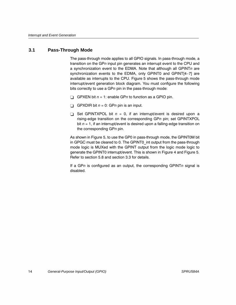
3.1 Pass-Through Mode
The pass-through mode applies to all GPIO signals. In pass-through mode, atransition on the GPn input pin generates an interrupt event to the CPU anda synchronization event to the EDMA. Note that although all GPINTn aresynchronization events to the EDMA, only GPINT0 and GPINT[4−7] areavailable as interrupts to the CPU. Figure 5 shows the pass-through modeinterrupt/event generation block diagram. You must configure the followingbits correctly to use a GPn pin in the pass-through mode:
� GPXEN bit n = 1: enable GPn to function as a GPIO pin.
� GPXDIR bit n = 0: GPn pin is an input.
� Set GPINTXPOL bit n = 0, if an interrupt/event is desired upon arising-edge transition on the corresponding GPn pin; set GPINTXPOLbit n = 1, if an interrupt/event is desired upon a falling-edge transition onthe corresponding GPn pin.
As shown in Figure 5, to use the GP0 in pass-through mode, the GPINT0M bitin GPGC must be cleared to 0. The GPINT0_int output from the pass-throughmode logic is MUXed with the GPINT output from the logic mode logic togenerate the GPINT0 interrupt/event. This is shown in Figure 4 and Figure 5.Refer to section 5.8 and section 3.3 for details.
If a GPn is configured as an output, the corresponding GPINTn signal isdisabled.
Interrupt and Event Generation
15General-Purpose Input/Output (GPIO)SPRU584A
Figure 5. GPINTn Generation in Pass-Through Mode
GP0 pin
GP15VAL
GP3VAL
GP0VALGPINT0_int
GPINT3
GPINT15
To interruptselector andEDMA events�
GPINT0POL
GPINT3POL
GPINT15POL
GP3 pin
GP15 pin
0
0
0
1
1
1
0
1
GPINT0M
GPINT signalfrom logic mode GPINT0
Applies to GPIO0 only.
� All GPINTn are synchronization events to the EDMA. Only GPINT0 and GPINT[4−7] are available as interrupts to the CPU.
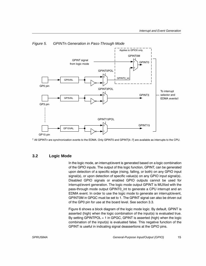
3.2 Logic Mode
In the logic mode, an interrupt/event is generated based on a logic combinationof the GPIO inputs. The output of this logic function, GPINT, can be generatedupon detection of a specific edge (rising, falling, or both) on any GPIO inputsignal(s), or upon detection of specific value(s) on any GPIO input signal(s).Disabled GPIO signals or enabled GPIO outputs cannot be used forinterrupt/event generation. The logic mode output GPINT is MUXed with thepass-through mode output GPINT0_int to generate a CPU interrupt and anEDMA event. In order to use the logic mode to generate an interrupt/event,GPINT0M in GPGC must be set to 1. The GPINT signal can also be driven outof the GP0 pin for use at the board level. See section 3.3.
Figure 6 shows a block diagram of the logic mode logic. By default, GPINT isasserted (high) when the logic combination of the input(s) is evaluated true.By setting GPINTPOL = 1 in GPGC, GPINT is asserted (high) when the logiccombination of the input(s) is evaluated false. This negative function of theGPINT is useful in indicating signal deassertions at the GPIO pins.
Interrupt and Event Generation
General-Purpose Input/Output (GPIO)16 SPRU584A
Figure 6. GPINT Generation in Logic Mode
GPINT0
GPINT0M
To CPUinterruptselector
and EDMAevents
Mask Logic for:
Delta ORDelta ANDValue AND
GPINTPOL
GPINT0_int
GPINT
From Pass ThroughMode Logic
GP0 pin
GP1 pin
GP15 pin
0
1
0
1
Logic Mode Logic
The GPINT generation operates in one of three modes: Delta OR, Delta AND,or Value AND. The GPINT generation is configured via two control bits inGPGC, GPINTDV and LOGIC, in addition to the mask bits in GPHM andGPLM. The GPINTDV bit in GPGC divides the logic mode into either Delta orValue mode as follows:
� Delta Mode: Inputs to the interrupt/event mask logic are sourced fromGPDH and GPDL. GPINT is caused by the logic combination of thetransition on the GPIO pin(s).
� Value Mode: Inputs to the interrupt/event mask logic are sourced fromGPVAL. GPINT is caused by the logic combination of the value on theGPIO pin(s).
The source to the logic mode mask logic is gated by GPHM and GPLM. In deltamode, the GPDH bit is gated with the GPHM bit and the GPDL bit is gated withthe GPLM bit. In value mode, the value from the pin is gated with the GPHMbit and the inverted value from the pin is gated with the GPLM bit.

Interrupt and Event Generation
17General-Purpose Input/Output (GPIO)SPRU584A
The LOGIC bit in GPGC controls whether an interrupt/event is generatedbased on all the mask outputs being true or any one of the mask outputs beingtrue:
� OR Mode: Interrupt/event generated based on any one of the maskoutputs being true.
� AND Mode: Interrupt/event generated based on all of the mask outputsbeing true.
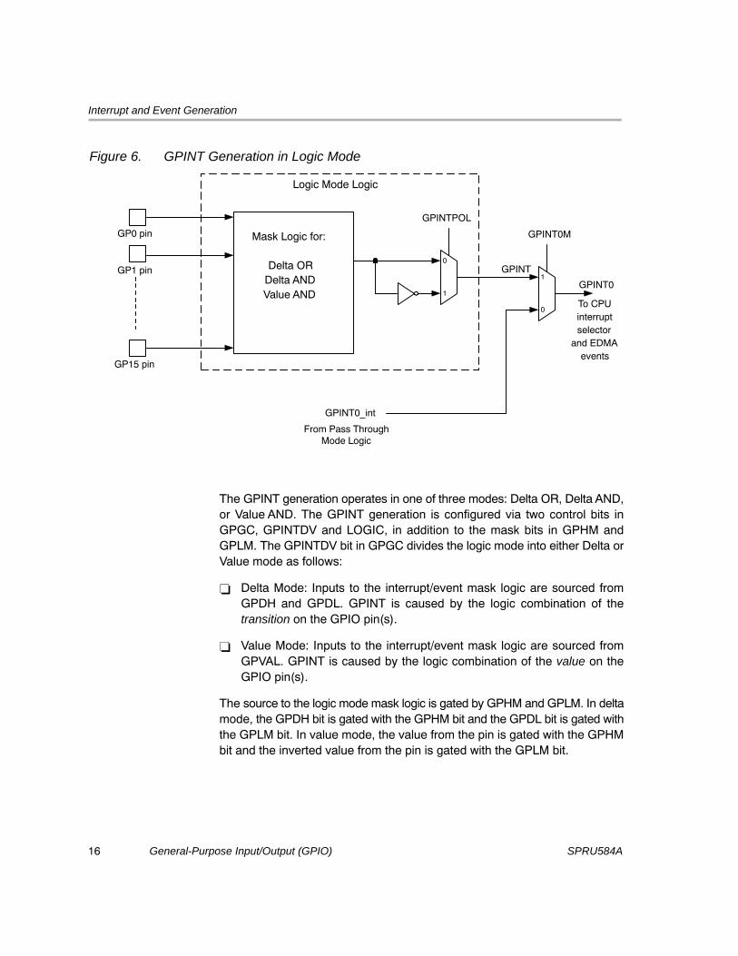
Table 1 summarizes the three modes in logic mode and the setup of theGPINTDV and LOGIC bits in GPGC.
Table 1. Logic Mode Truth Table
GPGC Bit
GPINTDV LOGIC Logic Mode Section
0 0 Delta OR 3.2.1
0 1 Delta AND 3.2.2
1 0 Reserved �
1 1 Value AND 3.2.3
In summary, GPGC must be configured as follows in logic mode:
� GPINT0M = 1 to enable logic mode interrupt/event generation. Theinterrupt/event signal to the DSP (GPINT0) is based on the logic functionoutput GPINT.
� GPINTPOL = 0 if the interrupt/event is based upon the logic evaluatingtrue; orGPINTPOL = 1 if the interrupt/event is based upon the logic evaluatingfalse.
� GPINTDV = 0 for Delta Mode, orGPINTDV = 1 for Value Mode.
� LOGIC = 0 for OR Mode, orLOGIC = 1 for AND Mode.
Interrupt and Event Generation
General-Purpose Input/Output (GPIO)18 SPRU584A
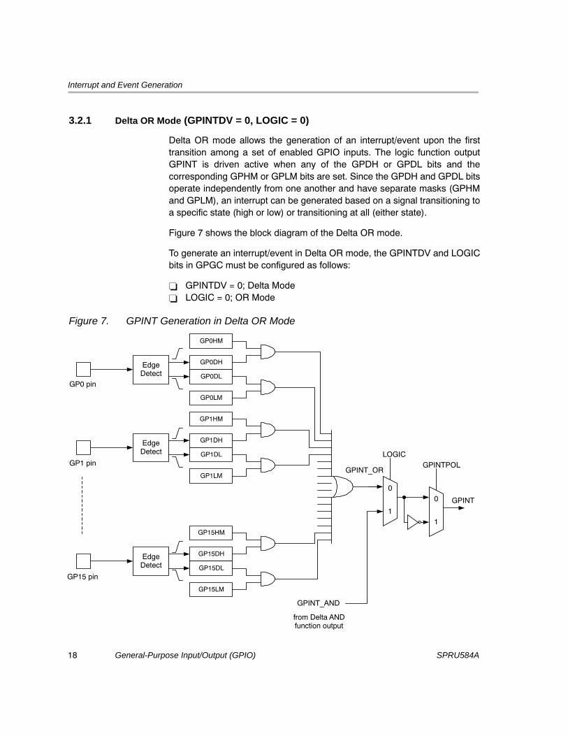
3.2.1 Delta OR Mode (GPINTDV = 0, LOGIC = 0)
Delta OR mode allows the generation of an interrupt/event upon the firsttransition among a set of enabled GPIO inputs. The logic function outputGPINT is driven active when any of the GPDH or GPDL bits and thecorresponding GPHM or GPLM bits are set. Since the GPDH and GPDL bitsoperate independently from one another and have separate masks (GPHMand GPLM), an interrupt can be generated based on a signal transitioning toa specific state (high or low) or transitioning at all (either state).
Figure 7 shows the block diagram of the Delta OR mode.
To generate an interrupt/event in Delta OR mode, the GPINTDV and LOGICbits in GPGC must be configured as follows:
� GPINTDV = 0; Delta Mode� LOGIC = 0; OR Mode
Figure 7. GPINT Generation in Delta OR Mode
EdgeDetect
GP0DH
GP0DL
GP0HM
GP0LM
EdgeDetect
GP1DH
GP1DL
GP1HM
GP1LM
EdgeDetect
GP15DH
GP15DL
GP15HM
GP15LM
GP0 pin
GPINT_OR
GPINT_AND
LOGIC
0
1
GPINTPOL
0
1
GPINT
GP1 pin
GP15 pin
from Delta ANDfunction output
Interrupt and Event Generation
19General-Purpose Input/Output (GPIO)SPRU584A
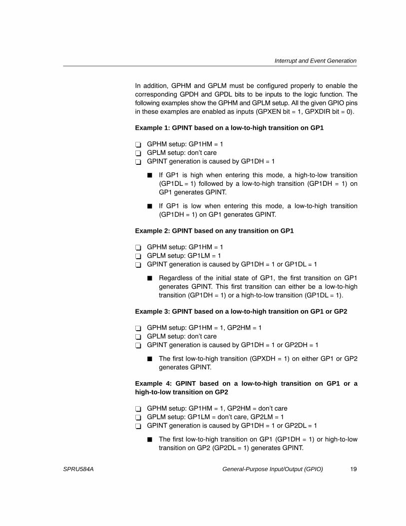
In addition, GPHM and GPLM must be configured properly to enable thecorresponding GPDH and GPDL bits to be inputs to the logic function. Thefollowing examples show the GPHM and GPLM setup. All the given GPIO pinsin these examples are enabled as inputs (GPXEN bit = 1, GPXDIR bit = 0).
Example 1: GPINT based on a low-to-high transition on GP1
� GPHM setup: GP1HM = 1� GPLM setup: don�t care� GPINT generation is caused by GP1DH = 1
� If GP1 is high when entering this mode, a high-to-low transition(GP1DL = 1) followed by a low-to-high transition (GP1DH = 1) onGP1 generates GPINT.
� If GP1 is low when entering this mode, a low-to-high transition(GP1DH = 1) on GP1 generates GPINT.
Example 2: GPINT based on any transition on GP1
� GPHM setup: GP1HM = 1� GPLM setup: GP1LM = 1� GPINT generation is caused by GP1DH = 1 or GP1DL = 1
� Regardless of the initial state of GP1, the first transition on GP1generates GPINT. This first transition can either be a low-to-hightransition (GP1DH = 1) or a high-to-low transition (GP1DL = 1).
Example 3: GPINT based on a low-to-high transition on GP1 or GP2
� GPHM setup: GP1HM = 1, GP2HM = 1� GPLM setup: don�t care� GPINT generation is caused by GP1DH = 1 or GP2DH = 1
� The first low-to-high transition (GPXDH = 1) on either GP1 or GP2generates GPINT.
Example 4: GPINT based on a low-to-high transition on GP1 or ahigh-to-low transition on GP2
� GPHM setup: GP1HM = 1, GP2HM = don�t care� GPLM setup: GP1LM = don�t care, GP2LM = 1� GPINT generation is caused by GP1DH = 1 or GP2DL = 1
� The first low-to-high transition on GP1 (GP1DH = 1) or high-to-lowtransition on GP2 (GP2DL = 1) generates GPINT.
Interrupt and Event Generation
General-Purpose Input/Output (GPIO)20 SPRU584A
Example 5: GPINT based on any transition on GP1 or GP2
� GPHM setup: GP1HM = 1, GP2HM = 1� GPLM setup: GP1LM = 1, GP2LM = 1� GPINT generation is caused by GP1DH, GP1DL, GP2DH, or GP2DL = 1
� The first transition on GP1 (GP1DH or GP1DL = 1) or the firsttransition on GP2 (GP2DH or GP2DL = 1) generates GPINT.
3.2.2 Delta AND Mode (GPINTDV = 0, LOGIC = 1)
Delta AND mode allows the generation of an interrupt/event after all of a setof specified signals have undergone some specified transitions. GPINT is drivenactive when both of the following conditions are true:
� All of the GPDH bits are asserted for the group of GPIO signals with theGPHM bits set.
� All of the GPDL bits are asserted for the group of GPIO signals with theGPLM bits set.
Since the GPDH and GPDL bits operate independently from one another andhave separate masks (GPHM and GPLM), GPINT can be generated based ona signal transitioning from one state to another and back to the original state.
To generate an interrupt/event in Delta AND mode, the GPINTDV and LOGICbits in GPGC must be configured as follows:
� GPINTDV = 0; Delta Mode� LOGIC = 1; AND Mode
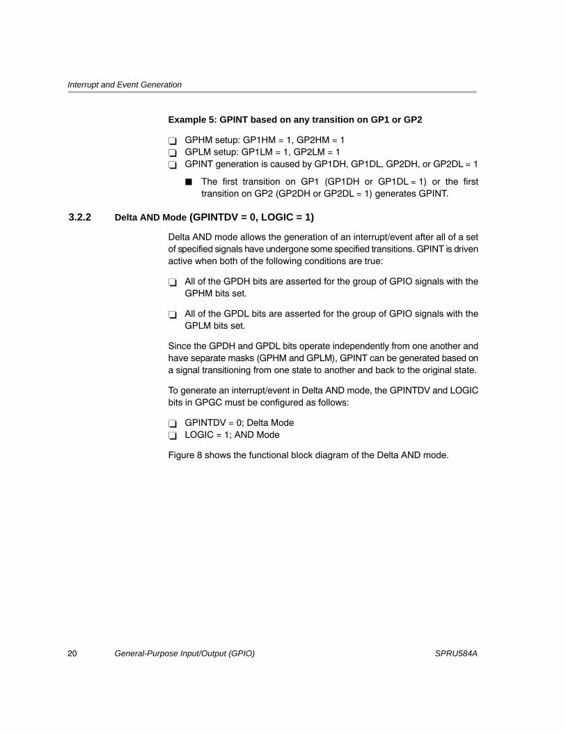
Figure 8 shows the functional block diagram of the Delta AND mode.
Interrupt and Event Generation
21General-Purpose Input/Output (GPIO)SPRU584A
Figure 8. GPINT Generation in Delta AND Mode
Edgedetect
GP0DH
GP0DL
GP0HM
GP0LM
Edgedetect
GP1DH
GP1DL
GP1HM
GP1LM
Edgedetect
GP15DH
GP15DL
GP15HM
GP15LM
GPINT_AND
LOGIC
GPINTPOL
GPINT
GP0 pin
GP1 pin
GP15 pin
0
10
1
GPINT_OR
from Delta ORfunction output
Note: The functional block diagram shows the mask logic as an OR with an inverter on the mask bit. This forces the OR toevaluate true when the mask bit is disabled. This is strictly a functional block diagram. The actual implementationprevents the GPINT from being asserted in the case that all of the mask bits are disabled.
In addition, GPHM and GPLM must be configured properly to enable thecorresponding GPDH and GPDL bits to be inputs to the logic function. Thefollowing examples show the GPHM and GPLM setup. All the given GPIO pinsin these examples are enabled as inputs (GPEN bit = 1, GPDIR bit = 0).
Example 1: GPINT based on a low-to-high transition on GP1
� GPHM setup: GP1HM = 1� GPLM setup: don�t care� GPINT generation is caused by GP1DH = 1
� If GP1 is high when entering this mode, a high-to-low transition(GP1DL = 1) followed by a low-to-high transition (GP1DH = 1) onGP1 generates GPINT.
� If GP1 is low when entering this mode, a low-to-high transition(GP1DH = 1) on GP1 generates GPINT.

Interrupt and Event Generation
General-Purpose Input/Output (GPIO)22 SPRU584A
Example 2: GPINT based on a low-to-high and a high-to-low transition onGP1
� GPHM setup: GP1HM = 1� GPLM setup: GP1LM = 1� GPINT generation is caused by GP1DH = 1 and GP1DL = 1
� If GP1 is high when entering this mode, a high-to-low transition(GP1DL = 1) followed by a low-to-high transition (GP1DH = 1) onGP1 generates GPINT.
� If GP1 is low when entering this mode, a low-to-high transition(GP1DH = 1) followed by a high-to-low transition (GP1DL = 1) onGP1 generates GPINT.
Example 3: GPINT based on a low-to-high transition on both GP1 andGP2
� GPHM setup: GP1HM = 1, GP2HM = 1� GPLM setup: don�t care� GPINT generation is caused by GP1DH = 1 and GP2DH = 1
� Both GP1 and GP2 must undergo a low-to-high transition(GP1DH = 1 and GP2DH = 1) to generate GPINT. If either (or both)signal starts out high, GPINT is not generated until this signalundergoes a high-to-low followed by a low-to-high transition.
Example 4: GPINT based on a low-to-high transition on GP1 and ahigh-to-low transition on GP2
� GPHM setup: GP1HM = 1, GP2HM = don�t care� GPLM setup: GP1LM = don�t care, GP2LM = 1� GPINT generation is caused by GP1DH = 1 and GP2DL = 1
� Regardless of the initial state, GP1 must undergo a low-to-high transition(GP1DH = 1) and GP2 must undergo a high-to-low transition(GP2DL = 1).
Example 5: GPINT based on a low-to-high and high-to-low transitions onboth GP1 and GP2
� GPHM setup: GP1HM = 1, GP2HM = 1� GPLM setup: GP1LM = 1, GP2LM = 1� GPINT generation is caused by GP1DH, GP1DL, GP2DH, and
GP2DL = 1
� Regardless of the initial state, both GP1 and GP2 must undergotransitions from original state back to original state.
Interrupt and Event Generation
23General-Purpose Input/Output (GPIO)SPRU584A
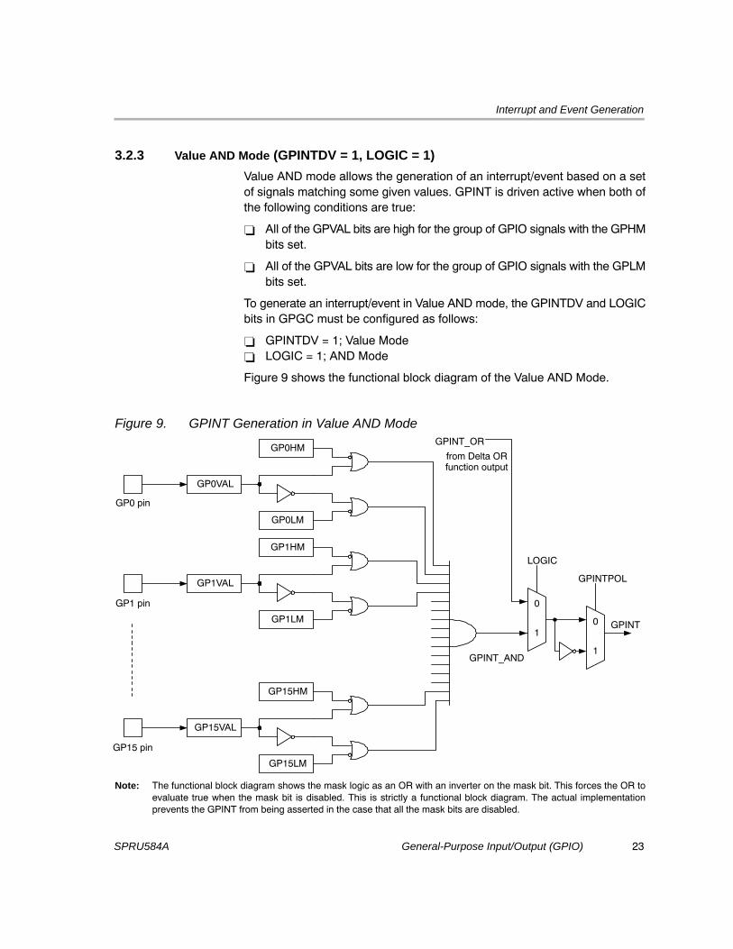
3.2.3 Value AND Mode (GPINTDV = 1, LOGIC = 1)
Value AND mode allows the generation of an interrupt/event based on a setof signals matching some given values. GPINT is driven active when both ofthe following conditions are true:
� All of the GPVAL bits are high for the group of GPIO signals with the GPHMbits set.
� All of the GPVAL bits are low for the group of GPIO signals with the GPLMbits set.
To generate an interrupt/event in Value AND mode, the GPINTDV and LOGICbits in GPGC must be configured as follows:
� GPINTDV = 1; Value Mode� LOGIC = 1; AND Mode
Figure 9 shows the functional block diagram of the Value AND Mode.
Figure 9. GPINT Generation in Value AND Mode
GP0HM
GP0LM
GP1HM
GP1LM
GP15VAL
GP15HM
GP15LM
GPINT_AND
LOGIC
GP1VAL
GP0VAL
GPINTPOL
GPINT
GP0 pin
GP15 pin
GP1 pin 0
10
1
GPINT_OR
from Delta ORfunction output
Note: The functional block diagram shows the mask logic as an OR with an inverter on the mask bit. This forces the OR toevaluate true when the mask bit is disabled. This is strictly a functional block diagram. The actual implementationprevents the GPINT from being asserted in the case that all the mask bits are disabled.
Interrupt and Event Generation
General-Purpose Input/Output (GPIO)24 SPRU584A
In addition, GPHM and GPLM must be configured properly to enable thecorresponding GPVAL bits to be inputs to the logic function. GPINT is notgenerated if any given GPIO signal has both GPHM and GPLM bits asserted.This is because no GPn (and the corresponding GPVAL bit n) can be both highand low simultaneously. The following examples show the GPHM and GPLMsetup. All the given GPIO pins in these examples are enabled as inputs(GPEN bit = 1, GPDIR bit = 0).
Example 1: GPINT based on GP1 = 1
� GPHM setup: GP1HM = 1� GPLM setup: GP1LM = 0� GPINT generation is caused by GP1 = 1
� If GP1 is high (GPXVAL = 1) when entering this mode, GPINT isimmediately asserted.
� If GP1 is low (GPXVAL = 0) when entering this mode, a low-to-hightransition (GPXVAL = 1) on GP1 generates GPINT.
Example 2: GPINT is not generated when GPnHM = GPnLM = 1
� GPHM setup: GP1HM = 1� GPLM setup: GP1LM = 1� GPINT is not generated because GP1 can never simultaneously be both
low (GPXVAL = 0) and high (GPXVAL = 1)
Example 3: GPINT based on GP1 = GP2 = 1
� GPHM setup: GP1HM = 1, GP2HM = 1� GPLM setup: GP1LM = 0, GP2LM = 0� GPINT generation is caused by GP1VAL = 1 and GP2VAL = 1
� If GP1 = GP2 = 1 when entering this mode, GPINT is immediatelyasserted.
� If GP1 = 1 and GP2 = 0 when entering this mode, a low-to-hightransition on GP2 (GP2VAL = 1), as GP1 stays high, generatesGPINT.
� If GP1 = GP2 = 0 when entering this mode, GPINT is generated whenboth GP1 and GP2 become high. If GP1 transitions high(GP1VAL = 1) then low (GP1VAL = 0) before GP2 transitions high, noGPINT is generated.

Interrupt and Event Generation
25General-Purpose Input/Output (GPIO)SPRU584A
Example 4: GPINT based on GP1 = 1 and GP2 = 0
� GPHM setup: GP1HM = 1, GP2HM = 0� GPLM setup: GP1LM = 0, GP2LM = 1� GPINT generation is caused by GP1VAL = 1 and GP2VAL = 0
� As in previous examples, both GP1 and GP2 must simultaneously beat the defined state: GP1VAL = 1 and GP2VAL = 0.
3.3 GPINT Muxing With GP0 and/or GPINT0
The logic function output signal GPINT can be used by both the DSP and anexternal device as follows:
� GPINT can generate a CPU interrupt and an EDMA event via GPINT0.
� If GP0 is configured as an output, GPINT can be driven out on GP0 to beused by external devices.
Figure 10 shows the connection of the GPINT signal.
Figure 10. GPINT Connection to GP0 and GPINT0
1
0 GP0VALGP0 pin
0
1GP0M
GPINT0M
GPINT0_int
GPINT
GPINT0
To CPU and EDMA
from pass through mode logic
from logic mode logic
GP0DIR
When GP0 is configured as an output (GP0DIR = 1), the GP0M bit controlswhether the GP0 signal operates in GPIO mode or in logic mode. In GPIOmode (GP0M = 0), the value of the GP0VAL bit is driven out on GP0. In logicmode (GP0M = 1), GPINT is driven out on GP0. When GP0 is configured asan input, GP0M has no effect.
Interrupts and Events
General-Purpose Input/Output (GPIO)26 SPRU584A
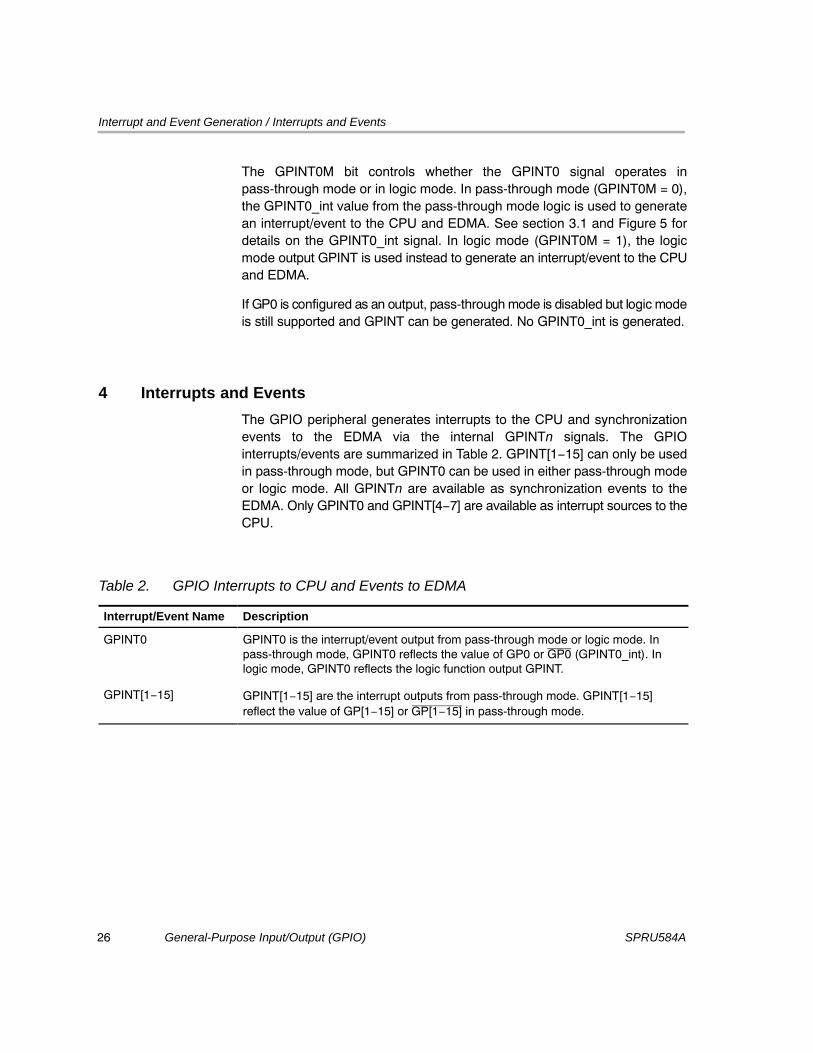
The GPINT0M bit controls whether the GPINT0 signal operates inpass-through mode or in logic mode. In pass-through mode (GPINT0M = 0),the GPINT0_int value from the pass-through mode logic is used to generatean interrupt/event to the CPU and EDMA. See section 3.1 and Figure 5 fordetails on the GPINT0_int signal. In logic mode (GPINT0M = 1), the logicmode output GPINT is used instead to generate an interrupt/event to the CPUand EDMA.
If GP0 is configured as an output, pass-through mode is disabled but logic modeis still supported and GPINT can be generated. No GPINT0_int is generated.
4 Interrupts and Events
The GPIO peripheral generates interrupts to the CPU and synchronizationevents to the EDMA via the internal GPINTn signals. The GPIOinterrupts/events are summarized in Table 2. GPINT[1−15] can only be usedin pass-through mode, but GPINT0 can be used in either pass-through modeor logic mode. All GPINTn are available as synchronization events to theEDMA. Only GPINT0 and GPINT[4−7] are available as interrupt sources to theCPU.
Table 2. GPIO Interrupts to CPU and Events to EDMA
Interrupt/Event Name Description
GPINT0 GPINT0 is the interrupt/event output from pass-through mode or logic mode. Inpass-through mode, GPINT0 reflects the value of GP0 or GP0 (GPINT0_int). Inlogic mode, GPINT0 reflects the logic function output GPINT.
GPINT[1−15] GPINT[1−15] are the interrupt outputs from pass-through mode. GPINT[1−15]reflect the value of GP[1−15] or GP[1−15] in pass-through mode.
Interrupt and Event Generation / Interrupts and Events

Registers
27General-Purpose Input/Output (GPIO)SPRU584A
5 Registers
The GPIO peripheral is configured through the registers listed in Table 3. Seethe device-specific datasheet for the memory address of these registers.
Table 3. GPIO Registers
Acronym Register Name Section
GPEN GPIO Enable Register 5.1
GPDIR GPIO Direction Register 5.2
GPVAL GPIO Value Register 5.3
GPDH GPIO Delta High Register 5.4
GPDL GPIO Delta Low Register 5.5
GPHM GPIO High Mask Register 5.6
GPLM GPIO Low Mask Register 5.7
GPGC GPIO Global Control Register 5.8
GPPOL GPIO Interrupt Polarity Register 5.9
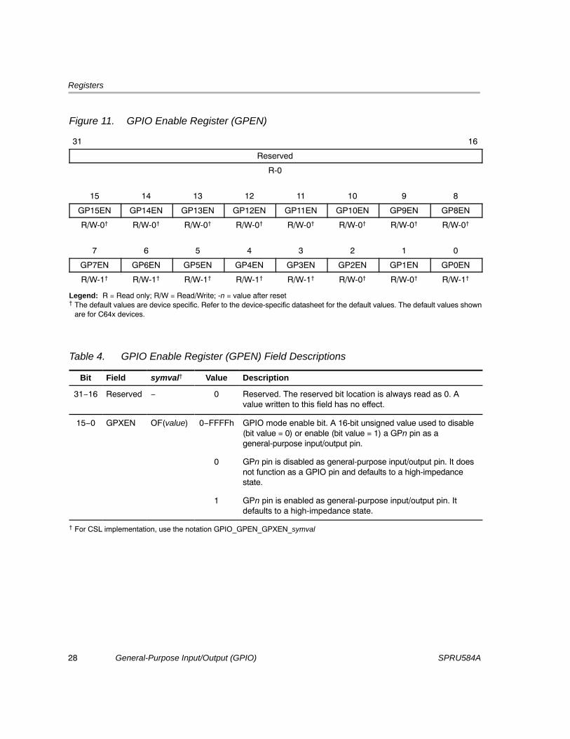
5.1 GPIO Enable Register (GPEN)
The GPIO enable register (GPEN) enables the GPIO pins for general-purposeinput/output functions. To use any of the GPIO pins in general-purposeinput/output mode, the corresponding GPXEN bit must be set to 1. The GPENis shown in Figure 11 and described in Table 4.
Some GPIO signals are MUXed with other device signals. For these MUXedsignals, the signal functionality is controlled by the following:
� Device configuration inputs: At reset, device configuration inputs selectthe MUXed signal to operate as either a GPIO pin or in the other mode.
� GPEN bit fields: A GPXEN bit n set to 1 indicates that the GPn pinoperates as a GPIO signal controlled by the remaining GPIO registers. AGPXEN bit n cleared to 0 indicates that the GPn pin is disabled as a GPIOpin; it operates in the other mode.
For details on signal configuration, refer to your device-specific datasheet.
Registers
General-Purpose Input/Output (GPIO)28 SPRU584A
Figure 11. GPIO Enable Register (GPEN)
31 16
Reserved
R-0
15 14 13 12 11 10 9 8
GP15EN GP14EN GP13EN GP12EN GP11EN GP10EN GP9EN GP8EN
R/W-0� R/W-0� R/W-0� R/W-0� R/W-0� R/W-0� R/W-0� R/W-0�
7 6 5 4 3 2 1 0
GP7EN GP6EN GP5EN GP4EN GP3EN GP2EN GP1EN GP0EN
R/W-1� R/W-1� R/W-1� R/W-1� R/W-1� R/W-0� R/W-0� R/W-1�
Legend: R = Read only; R/W = Read/Write; -n = value after reset� The default values are device specific. Refer to the device-specific datasheet for the default values. The default values shown
are for C64x devices.
Table 4. GPIO Enable Register (GPEN) Field Descriptions
Bit Field symval� Value Description
31−16 Reserved − 0 Reserved. The reserved bit location is always read as 0. Avalue written to this field has no effect.
15−0 GPXEN OF(value) 0−FFFFh GPIO mode enable bit. A 16-bit unsigned value used to disable(bit value = 0) or enable (bit value = 1) a GPn pin as ageneral-purpose input/output pin.
0 GPn pin is disabled as general-purpose input/output pin. It doesnot function as a GPIO pin and defaults to a high-impedancestate.
1 GPn pin is enabled as general-purpose input/output pin. Itdefaults to a high-impedance state.
� For CSL implementation, use the notation GPIO_GPEN_GPXEN_symval

Registers
29General-Purpose Input/Output (GPIO)SPRU584A
5.2 GPIO Direction Register (GPDIR)
The GPIO direction register (GPDIR) determines if a given GPIO pin is an inputor an output. GPDIR only applies if the corresponding GPIO signal is enabledvia the GPXEN bits in GPEN. The GPDIR is shown in Figure 12 and describedin Table 5. By default, all the GPIO pins are configured as input pins.
When GPIO pins are configured as output pins, these pins do not havehigh-impedance capability. At reset, GPIO output pins default to the value inthe GPIO value register (GPVAL), see section 5.3. If it is necessary to drive theGPIO output to the high-impedance state, the GPIO pins can be configuredas an input pin and then changed to an output pin.
Figure 12. GPIO Direction Register (GPDIR)
31 16
Reserved
R-0
15 14 13 12 11 10 9 8
GP15DIR GP14DIR GP13DIR GP12DIR GP11DIR GP10DIR GP9DIR GP8DIR
R/W-0 R/W-0 R/W-0 R/W-0 R/W-0 R/W-0 R/W-0 R/W-0
7 6 5 4 3 2 1 0
GP7DIR GP6DIR GP5DIR GP4DIR GP3DIR GP2DIR GP1DIR GP0DIR
R/W-0 R/W-0 R/W-0 R/W-0 R/W-0 R/W-0 R/W-0 R/W-0
Legend: R = Read only; R/W = Read/Write; -n = value after reset
Table 5. GPIO Direction Register (GPDIR) Field Descriptions
Bit Field symval� Value Description
31−16 Reserved − 0 Reserved. The reserved bit location is always read as 0. Avalue written to this field has no effect.
15−0 GPXDIR OF(value) 0−FFFFh GPn direction bit. A 16-bit unsigned value used to control thedirection (input = 0, output = 1) of a GPn pin. Applies when thecorresponding GPXEN bit in GPEN is set to 1.
0 GPn pin is an input.
1 GPn pin is an output.
� For CSL implementation, use the notation GPIO_GPDIR_GPXDIR_symval

Registers
General-Purpose Input/Output (GPIO)30 SPRU584A
5.3 GPIO Value Register (GPVAL)
The GPIO value register (GPVAL) indicates the value to be driven on a givenGPIO output pin or the value detected on a given GPIO input pin. The GPVALis shown in Figure 13 and described in Table 6.
Figure 13. GPIO Value Register (GPVAL)
31 16
Reserved
R-0
15 14 13 12 11 10 9 8
GP15VAL GP14VAL GP13VAL GP12VAL GP11VAL GP10VAL GP9VAL GP8VAL
R/W-0 R/W-0 R/W-0 R/W-0 R/W-0 R/W-0 R/W-0 R/W-0
7 6 5 4 3 2 1 0
GP7VAL GP6VAL GP5VAL GP4VAL GP3VAL GP2VAL GP1VAL GP0VAL
R/W-0 R/W-0 R/W-0 R/W-0 R/W-0 R/W-0 R/W-0 R/W-0
Legend: R = Read only; R/W = Read/Write; -n = value after reset
Table 6. GPIO Value Register (GPVAL) Field Descriptions
Bit Field symval� Value Description
31−16 Reserved − 0 Reserved. The reserved bit location is always read as 0. Avalue written to this field has no effect.
15−0 GPXVAL OF(value) 0−FFFFh GPn value bit. A 16-bit unsigned value used to determine thevalue detected at a GPn input/output pin. Applies when thecorresponding GPXEN bit in GPEN is set to 1.
When GPn pin is an input (GPXDIR = 0).
0 A value of 0 is latched from the GPn input pin.
1 A value of 1 is latched from the GPn input pin.
When GPn pin is an output (GPXDIR = 1).
0 GPn signal is driven low.
1 GPn signal is driven high.
� For CSL implementation, use the notation GPIO_GPVAL_GPXVAL_symval

Registers
31General-Purpose Input/Output (GPIO)SPRU584A
5.4 GPIO Delta High Register (GPDH)
The GPIO delta high register (GPDH) indicates whether a given GPIO inputhas undergone a low-to-high transition. If the given GPIO pin is configured asan output, the corresponding bit in GPDH maintains its previous value. Writinga 1 to the corresponding bit clears the bit, writing a 0 has no effect. The GPDHis shown in Figure 14 and described in Table 7.
Figure 14. GPIO Delta High Register (GPDH)
31 16
Reserved
R-0
15 14 13 12 11 10 9 8
GP15DH GP14DH GP13DH GP12DH GP11DH GP10DH GP9DH GP8DH
R/W-0 R/W-0 R/W-0 R/W-0 R/W-0 R/W-0 R/W-0 R/W-0
7 6 5 4 3 2 1 0
GP7DH GP6DH GP5DH GP4DH GP3DH GP2DH GP1DH GP0DH
R/W-0 R/W-0 R/W-0 R/W-0 R/W-0 R/W-0 R/W-0 R/W-0
Legend: R = Read only; R/W = Read/Write; -n = value after reset
Table 7. GPIO Delta High Register (GPDH) Field Descriptions
Bit Field symval� Value Description
31−16 Reserved − 0 Reserved. The reserved bit location is always read as 0. Avalue written to this field has no effect.
15−0 GPXDH OF(value) 0−FFFFh GPn delta high bit. A 16-bit unsigned value used to determine ifa low-to-high transition is detected on the GPn input pin.Applies when the corresponding GPn pin is enabled as aninput (GPXEN = 1 and GPXDIR = 0).
0 A low-to-high transition is not detected on GPn pin.
1 A low-to-high transition is detected on GPn pin.
� For CSL implementation, use the notation GPIO_GPDH_GPXDH_symval

Registers
General-Purpose Input/Output (GPIO)32 SPRU584A
5.5 GPIO Delta Low Register (GPDL)
The GPIO delta low register (GPDL) indicates whether a given GPIO input hasundergone a high-to-low transition. If the given GPIO pin is configured as anoutput, the corresponding bit in GPDL maintains its previous value. Writing a1 to the corresponding bit clears the bit, writing a 0 has no effect. The GPDLis shown in Figure 15 and described in Table 8.
Figure 15. GPIO Delta Low Register (GPDL)
31 16
Reserved
R-0
15 14 13 12 11 10 9 8
GP15DL GP14DL GP13DL GP12DL GP11DL GP10DL GP9DL GP8DL
R/W-0 R/W-0 R/W-0 R/W-0 R/W-0 R/W-0 R/W-0 R/W-0
7 6 5 4 3 2 1 0
GP7DL GP6DL GP5DL GP4DL GP3DL GP2DL GP1DL GP0DL
R/W-0 R/W-0 R/W-0 R/W-0 R/W-0 R/W-0 R/W-0 R/W-0
Legend: R = Read only; R/W = Read/Write; -n = value after reset
Table 8. GPIO Delta Low Register (GPDL) Field Descriptions
Bit Field symval� Value Description
31−16 Reserved − 0 Reserved. The reserved bit location is always read as 0. Avalue written to this field has no effect.
15−0 GPXDL OF(value) 0−FFFFh GPn delta low bit. A 16-bit unsigned value used to determine ifa high-to-low transition is detected on the GPn input pin.Applies when the corresponding GPn pin is enabled as aninput (GPXEN = 1 and GPXDIR = 0).
0 A high-to-low transition is not detected on GPn pin.
1 A high-to-low transition is detected on GPn pin.
� For CSL implementation, use the notation GPIO_GPDL_GPXDL_symval

Registers
33General-Purpose Input/Output (GPIO)SPRU584A
5.6 GPIO High Mask Register (GPHM)The GPIO high mask register (GPHM) is used to enable a given GPIO inputto cause a CPU interrupt or an EDMA event generation. If a GPHM bit(GPnHM) is disabled, the value or transition on the corresponding GPn pindoes not cause an interrupt/event generation. If the mask bit is enabled, thecorresponding GPn input may cause an interrupt/event to be generateddepending on the interrupt mode selected in GPGC. Refer to section 3 fordetails on the function of GPHM in interrupt/event generation. The GPHM isshown in Figure 16 and described in Table 9.
Figure 16. GPIO High Mask Register (GPHM)
31 16
Reserved
R-0
15 14 13 12 11 10 9 8
GP15HM GP14HM GP13HM GP12HM GP11HM GP10HM GP9HM GP8HM
R/W-0 R/W-0 R/W-0 R/W-0 R/W-0 R/W-0 R/W-0 R/W-0
7 6 5 4 3 2 1 0
GP7HM GP6HM GP5HM GP4HM GP3HM GP2HM GP1HM GP0HM
R/W-0 R/W-0 R/W-0 R/W-0 R/W-0 R/W-0 R/W-0 R/W-0
Legend: R = Read only; R/W = Read/Write; -n = value after reset
Table 9. GPIO High Mask Register (GPHM) Field Descriptions
Bit Field symval� Value Description
31−16 Reserved − 0 Reserved. The reserved bit location is always read as 0. Avalue written to this field has no effect.
15−0 GPXHM OF(value) 0−FFFFh GPn high mask bit. A 16-bit unsigned value used to disable (bitvalue = 0) or enable (bit value = 1) an interrupt/event generationbased on either the corresponding GPXDH bit or GPXVAL bit.Applies when the corresponding GPn pin is enabled as aninput (GPXEN = 1 and GPXDIR = 0).
0 Interrupt/event generation is disabled for GPn pin. The value ortransition on GPn pin does not cause an interrupt/eventgeneration.
1 Interrupt/event generation is enabled for GPn pin.
� For CSL implementation, use the notation GPIO_GPHM_GPXHM_symval
Registers
General-Purpose Input/Output (GPIO)34 SPRU584A
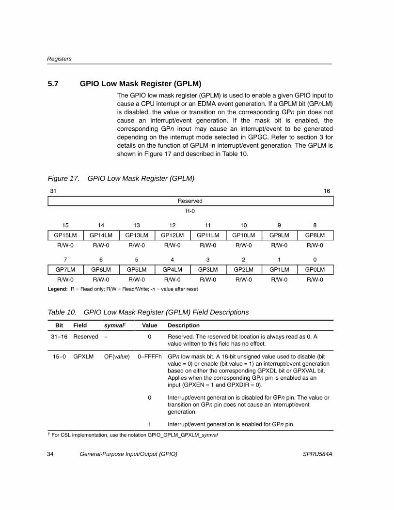
5.7 GPIO Low Mask Register (GPLM)The GPIO low mask register (GPLM) is used to enable a given GPIO input tocause a CPU interrupt or an EDMA event generation. If a GPLM bit (GPnLM)is disabled, the value or transition on the corresponding GPn pin does notcause an interrupt/event generation. If the mask bit is enabled, thecorresponding GPn input may cause an interrupt/event to be generateddepending on the interrupt mode selected in GPGC. Refer to section 3 fordetails on the function of GPLM in interrupt/event generation. The GPLM isshown in Figure 17 and described in Table 10.
Figure 17. GPIO Low Mask Register (GPLM)
31 16
Reserved
R-0
15 14 13 12 11 10 9 8
GP15LM GP14LM GP13LM GP12LM GP11LM GP10LM GP9LM GP8LM
R/W-0 R/W-0 R/W-0 R/W-0 R/W-0 R/W-0 R/W-0 R/W-0
7 6 5 4 3 2 1 0
GP7LM GP6LM GP5LM GP4LM GP3LM GP2LM GP1LM GP0LM
R/W-0 R/W-0 R/W-0 R/W-0 R/W-0 R/W-0 R/W-0 R/W-0
Legend: R = Read only; R/W = Read/Write; -n = value after reset
Table 10. GPIO Low Mask Register (GPLM) Field Descriptions
Bit Field symval� Value Description
31−16 Reserved − 0 Reserved. The reserved bit location is always read as 0. Avalue written to this field has no effect.
15−0 GPXLM OF(value) 0−FFFFh GPn low mask bit. A 16-bit unsigned value used to disable (bitvalue = 0) or enable (bit value = 1) an interrupt/event generationbased on either the corresponding GPXDL bit or GPXVAL bit.Applies when the corresponding GPn pin is enabled as aninput (GPXEN = 1 and GPXDIR = 0).
0 Interrupt/event generation is disabled for GPn pin. The value ortransition on GPn pin does not cause an interrupt/eventgeneration.
1 Interrupt/event generation is enabled for GPn pin.
� For CSL implementation, use the notation GPIO_GPLM_GPXLM_symval

Registers
35General-Purpose Input/Output (GPIO)SPRU584A
5.8 GPIO Global Control Register (GPGC)
The GPIO global control register (GPGC) configures the interrupt/eventgeneration of the GPIO peripheral. The GPGC is shown in Figure 18 anddescribed in Table 11.
Figure 18. GPIO Global Control Register (GPGC)
31 8
Reserved
R-0
7 6 5 4 3 2 1 0
Reserved GP0M GPINT0M Reserved GPINTPOL LOGIC GPINTDV
R-0 R/W-0 R/W-0 R-0 R/W-0 R/W-0 R/W-0
Legend: R = Read only; R/W = Read/Write; -n = value after reset
Table 11. GPIO Global Control Register (GPGC) Field Descriptions
Bit field� symval� Value Description
31−6 Reserved − 0 Reserved. The reserved bit location is always read as 0. Avalue written to this field has no effect.
5 GP0M GP0 output mode bit. Applies only if GP0 is configured asan output (GPXDIR bit 0 = 1).
GPIOMODE 0 GPIO mode�GP0 output is based on GP0 value (GPXVALbit 0 value in GPVAL).
LOGICMODE 1 Logic mode�GP0 output is based on value of internal logicmode interrupt/event signal GPINT.
4 GPINT0M GPINT0 interrupt/event generation mode bit.
PASSMODE 0 Pass-through mode�GPINT0 interrupt/event generation isbased on GP0 input value (GPXVAL bit 0 value in GPVAL).
LOGICMODE 1 Logic Mode�GPINT0 interrupt/event generation is basedon GPINT.
3 Reserved − 0 Reserved. The reserved bit location is always read as 0. Avalue written to this field has no effect.
� For CSL implementation, use the notation GPIO_GPGC_field_symval
Registers
General-Purpose Input/Output (GPIO)36 SPRU584A
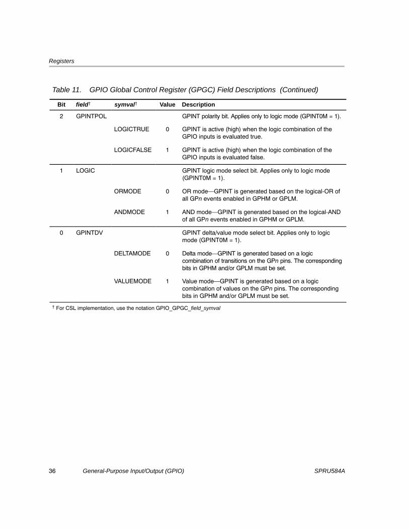
Table 11. GPIO Global Control Register (GPGC) Field Descriptions (Continued)
DescriptionValuesymval�field�Bit
2 GPINTPOL GPINT polarity bit. Applies only to logic mode (GPINT0M = 1).
LOGICTRUE 0 GPINT is active (high) when the logic combination of theGPIO inputs is evaluated true.
LOGICFALSE 1 GPINT is active (high) when the logic combination of theGPIO inputs is evaluated false.
1 LOGIC GPINT logic mode select bit. Applies only to logic mode(GPINT0M = 1).
ORMODE 0 OR mode�GPINT is generated based on the logical-OR ofall GPn events enabled in GPHM or GPLM.
ANDMODE 1 AND mode�GPINT is generated based on the logical-ANDof all GPn events enabled in GPHM or GPLM.
0 GPINTDV GPINT delta/value mode select bit. Applies only to logicmode (GPINT0M = 1).
DELTAMODE 0 Delta mode�GPINT is generated based on a logiccombination of transitions on the GPn pins. The correspondingbits in GPHM and/or GPLM must be set.
VALUEMODE 1 Value mode�GPINT is generated based on a logiccombination of values on the GPn pins. The correspondingbits in GPHM and/or GPLM must be set.
� For CSL implementation, use the notation GPIO_GPGC_field_symval
Registers
37General-Purpose Input/Output (GPIO)SPRU584A
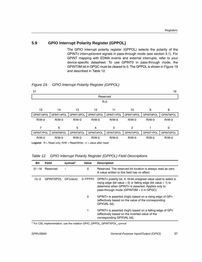
5.9 GPIO Interrupt Polarity Register (GPPOL)
The GPIO interrupt polarity register (GPPOL) selects the polarity of theGPINTn interrupt/event signals in pass-through mode (see section 3.1). ForGPINT mapping with EDMA events and external interrupts, refer to yourdevice-specific datasheet. To use GPINT0 in pass-through mode, theGPINT0M bit in GPGC must be cleared to 0. The GPPOL is shown in Figure 19and described in Table 12.
Figure 19. GPIO Interrupt Polarity Register (GPPOL)
31 16
Reserved
R-0
15 14 13 12 11 10 9 8
GPINT15POL GPINT14POL GPINT13POL GPINT12POL GPINT11POL GPINT10POL GPINT9POL GPINT8POL
R/W-0 R/W-0 R/W-0 R/W-0 R/W-0 R/W-0 R/W-0 R/W-0
7 6 5 4 3 2 1 0
GPINT7POL GPINT6POL GPINT5POL GPINT4POL GPINT3POL GPINT2POL GPINT1POL GPINT0POL
R/W-0 R/W-0 R/W-0 R/W-0 R/W-0 R/W-0 R/W-0 R/W-0
Legend: R = Read only; R/W = Read/Write; -n = value after reset
Table 12. GPIO Interrupt Polarity Register (GPPOL) Field Descriptions
Bit Field symval� Value Description
31−16 Reserved − 0 Reserved. The reserved bit location is always read as zero.A value written to this field has no effect.
15−0 GPINTXPOL OF(value) 0−FFFFh GPINTn polarity bit. A 16-bit unsigned value used to select arising edge (bit value = 0) or falling edge (bit value = 1) todetermine when GPINTn is asserted. Applies only topass-through mode (GPINT0M = 0 in GPGC).
0 GPINTn is asserted (high) based on a rising edge of GPn(effectively based on the value of the correspondingGPXVAL bit).
1 GPINTn is asserted (high) based on a falling edge of GPn(effectively based on the inverted value of thecorresponding GPXVAL bit).
� For CSL implementation, use the notation GPIO_GPPOL_GPINTXPOL_symval

General-Purpose Input/Output (GPIO)38 SPRU584A
This page is intentionally left blank.

39General-Purpose Input/Output (GPIO)SPRU584A
Revision History
Table 13 lists the changes made since the previous version of this document.
Table 13. Document Revision History
Page Additions/Modifications/Deletions
This document has been reviewed for accuracy and there are no changes since the previousversion (July 2003) of this document.

General-Purpose Input/Output (GPIO)40 SPRU584A
This page is intentionally left blank.
Index
41General-Purpose Input/Output (GPIO)SPRU584A
Index
Bblock diagram
C64x DSP 9event generation 13functional 12GPINT generation in delta AND mode 21GPINT generation in delta OR mode 18GPINT generation in logic mode 16GPINT generation in value AND mode 23 25GPINTn generation in pass-through mode 15GPIO 10interrupt generation 13
Ddelta AND mode 20
delta OR mode 18
Eevent generation 13events 26
Ffunction 11
GGP0M bit 35GPDH 31
GPDIR 29GPDL 32
GPEN 27
GPGC 35GPHM 33GPINT muxing with GP0 and/or GPINT0 25GPINT0M bit 35GPINTDV bit 35GPINTPOL bit 35GPINTXPOL bits 37GPIO delta high register (GPDH) 31GPIO delta low register (GPDL) 32GPIO direction register (GPDIR) 29GPIO enable register (GPEN) 27GPIO global control register (GPGC) 35GPIO high mask register (GPHM) 33GPIO interrupt polarity register (GPPOL) 37GPIO low mask register (GPLM) 34GPIO value register (GPVAL) 30GPLM 34GPPOL 37GPVAL 30GPXDH bits 31GPXDIR bits 29GPXDL bits 32GPXEN bits 28GPXHM bits 33GPXLM bits 34GPXVAL bits 30
Iinterrupt and event generation
logic mode 15pass-through mode 14
interrupt generation 13interrupts 26

Index
42 General-Purpose Input/Output (GPIO) SPRU584A
LLOGIC bit 35
logic mode 15
Nnotational conventions 3
Ooverview 9
Ppass-through mode 14
Rregisters 27
GPIO delta high register (GPDH) 31GPIO delta low register (GPDL) 32GPIO direction register (GPDIR) 29GPIO enable register (GPEN) 27GPIO global control register (GPGC) 35GPIO high mask register (GPHM) 33GPIO interrupt polarity register (GPPOL) 37GPIO low mask register (GPLM) 34GPIO value register (GPVAL) 30
related documentation from Texas Instruments 3revision history 39
Ttrademarks 4
Vvalue AND mode 23