tmc6130 datasheet µc bldc motor -...
TRANSCRIPT

POWER DRIVER FOR STEPPER MOTORS INTEGRATED CIRCUITS
TRINAMIC Motion Control GmbH & Co. KG Hamburg, Germany
TMC6130 DATASHEET
BLOCK DIAGRAM
DriverLogic
EEPROM
3.3V
SPI
ENABLE
BHx
BLx
VCCCharge Pump
VM
Power on reset
12VRegulator
RC Oscillator
Current Measurement
ERROR
+VM
HS
LS
BLDC Motor
NS
VREF
OvervoltageUndervoltage
Overtemperature
Diagnostics &Error Feedback
Diagn. Comp.
CURRENTGNDA GNDP
µC
BUS / IO
LS-DriveLS-DriveHS-Drive
LS-DriveLS-DriveLS-Drive
RSHUNT
RS-
RS+
VMON
TMC6130
Power
FEATURES AND BENEFITS
Level Shifting: µC PWM outputs / 6 or 3 ext. N-FET half-bridges
100% PWM Operation
Low Offset, Low Drift, Fast Current Sense Amplifier with configurable input range
Operating Range VM = [4.5, 28]V, 32V abs. max
Fault Interrupt & Feedback to microcontroller
Fastest settling time and minimum noise
Diagnostics: overcurrent, overtemperature, undervoltage
Configurable communication interface for diagnostics feedback
Drain-Source Voltage / Gate-Source Voltage external FET monitoring for short circuit protection
Sleep Mode with low quiescent current (<30µA)
Compatible with 3V and 5V microcontrollers
Charge-Pump provides NFET reverse polarity drive
Small Size: QFN 5x5mm package, 32 pins
APPLICATIONS
Battery operated equipment Handcraft gear Professional healthcare Fail-safe applications Low-torque control applications BLDC sine wave applications Positioning Actuators Factory Automation Pumps and Valves CNC Machines
DESCRIPTION
The TMC6130 is a high-current motor driver for compact and energy efficient BLDC solutions. It is designed to drive N-type FET 3-phase motor control applications and contains all power and analog circuitry required for a high performance system. The built-in EEPROM allows extensive configurability without the need for external resistors and SPI interface programming. This reduces the pin count to only 32. All output voltages are monitored and controlled. The device comprises a current shunt amplifier with a high gain bandwidth (GBW), offering a fast settling time with low noise. A combination of bootstrap and charge pump enables driving 6 (or 3) NFETs, with gate charges up to 400nC/NFET with a minimum of device self-heating. Further, the IC reset level below 4.5V allows also for low-voltage operation.
Cost-effective high-current BLDC motor driver with state-of-the-art feature set.
Fastest settling time and built-in EEPROM for extensive configuration.

TMC6130 DATASHEET (Rev. 1.00 / 2016-OCT-28) 2
www.trinamic.com
APPLICATION EXAMPLES: HIGH POWER – FASTEST SETTLING TIME
The TMC6130 3-phase motor pre-driver scores with a very fast settling time, high reliability, and broad diagnostic and safety features. It can be used within a large operating range from battery systems on up to 24V DC. This versatility covers a wide spectrum of applications and motor sizes, all while keeping costs down. Several safe operating features are integrated, including diagnostics related to all output voltages, power on reset, and short circuit protection. Diagnostics feedback is communicated to the microcontroller via a bidirectional error interface. Finally, this BLDC driver chip features a low side shunt amplifier with large gain bandwidth (GBW), ideal for torque control applications requiring very fast settling time and minimum noise. Extensive support at the chip, board, and software levels enables rapid design cycles and fast time-to-market with competitive products.
µC
PWM
High-Level Interface
Error
TMC6130
Position
Layout with MOSFET power module (B6-bridge)
ORDER CODES
Order code Description Size [mm2]
TMC6130-LA BLDC 3-phase driver, QFN32 5 x 5
TMC6130-EVAL Evaluation board for TMC6130. 80 x 115
TMC6130 EVALUATION BOARD
This evaluation board is a development platform for applications based on the TMC6130 three phase BLDC motor driver chip. Supply voltages are 4.5… 28V DC (max. 32V). The board features an embedded microcontroller with USB and RS232 (TTL level) interfaces for communication. The board offers test points for all pins of the TMC6130. For positioning, three digital hall sensors can be connected as well as an ABN encoder. Using the IOs, potentiometers and switches can be attached. TRINAMICs TMCM-BLDC software tool (running under Windows) enables access to all functions of the TMC6130 from a PC.

TMC6130 DATASHEET (Rev. 1.00 / 2016-OCT-28) 3
www.trinamic.com
TABLE OF CONTENTS
1 PRINCIPLES OF OPERATION ......................... 4
1.1 KEY CONCEPTS ............................................... 4 1.2 APPLICATION CIRCUITS ................................. 5
2 PIN ASSIGNMENTS ........................................... 8
2.1 PACKAGE OUTLINE ......................................... 8 2.2 SIGNAL DESCRIPTIONS .................................. 8
3 CURRENTS AND CURRENT CONTROL ........ 10
3.1 SUPPLY SYSTEMS ......................................... 10 3.2 100% PWM WITH BOOTSTRAP .................. 11 3.3 CURRENT CONSUMPTION IN SLEEP MODE .... 11
4 DIAGNOSTICS .................................................. 13
4.1 ERROR INTERFACE ...................................... 13 4.2 HARDWARE PROTECTION ............................. 15
5 EEPROM DEFAULT CONFIGURATION ......... 16
5.1 BASIC INFORMATION FOR SPI COMMUNICATION 17
6 SENSE AMPLIFIER ........................................... 18
6.1 SENSE AMPLIFIER CURRENT RANGES: EXAMPLES FOR 1MΩ SHUNT 19
7 FET DRIVER IMPLEMENTATION .................. 20
7.1 NORMAL OPERATION ................................... 20 7.2 FET DRIVER DURING SLEEP MODE .............. 20
8 ABSOLUTE MAXIMUM RATINGS ................. 21
9 GENERAL ELECTRICAL SPECIFICATIONS.. 22
9.1 OPERATIONAL RANGE (UNLESS OTHERWISE SPECIFIED) 22
10 PACKAGE MECHANICAL DATA .................... 29
10.1 QFN32 DIMENSIONAL DRAWINGS .............. 29 10.2 PACKAGE CODE ............................................ 29
11 DISCLAIMER ..................................................... 30
12 ESD SENSITIVE DEVICE ................................ 30
13 TABLE OF FIGURES ......................................... 31
14 REVISION HISTORY ....................................... 32
15 REFERENCES ...................................................... 32

TMC6130 DATASHEET (Rev. 0.90 / 2016-OCT-28) 4
www.trinamic.com
1 Principles of Operation
LS-DriveLS-DriveHigh Side
LS-DriveLS-DriveLow Side
DriverLogic
EEPROM
3.3V
SPI
Charge Pump
Power on reset
12VRegulator
RC Oscillator
OvervoltageUndervoltage
Overtemperature
Diagnostics &Error Feedback
Diagn. Comp.
Band Gap
ENABLE
BHx
BLx
VCC
VM
ERROR
VMON
GNDA
3
VCPVCP_SW
To Drivers
VCP_REG
DiagnosticsVCP_BOOST OV
DiagnosticsVCP_REG OV
DiagnosticsVCP_REG UV
DiagnosticsVGS UV
DiagnosticsVDST OV
VMON
VCPx
HSx
3
3
LSx
BMx 3
3
RshuntCurrent Measurement
DiagnosticsVDSB OV
RS+
RS-
VBAT
Cboost
VREFCURRENT GNDP
Figure 1.1 Block diagram and principle operation circuit
1.1 Key Concepts The TMC6130 BLDC motor pre-driver implements advanced features which contribute toward energy efficiency, high precision, high reliability, smooth motion, and cool operation in industrial BLDC motor applications.
Configuration All configurations are done. The TMC6130 is equipped with a programmed EEPROM in order to simplify the design-in. In almost all cases the default values will fit. Nevertheless, special configurations are possible, if necessary.
Interfacing The TMC6130 communicates with the microcontroller using the ERROR input/output for diagnostic feedback. During stand still, the SPI interface on the pre-driver can be used for configuration purposes. Further, it is possible to communicate via bit banging.
Fast Settling Time The TMC6130 offers an extremely short settling time. The shunt amplifier has a high gain bandwidth (GBW) to reach a fast settling time with minimum noise.
Voltage The TMC6130 can be used within the range of 4.5V to 28V DC.
Boost Current For quick motor reaction on a target setting, a higher boost current can be used. This way, the time interval for acceleration and deceleration can be shortened.
Sleep Mode In sleep mode, the current consumption can be reduced to or below 30µA.
TRINAMIC motor drivers also offer safeguards to detect/protect from shorted outputs, overtemperature, overvoltage, and undervoltage conditions.
TMC6130 DATASHEET (Rev. 0.90 / 2016-OCT-28) 5
www.trinamic.com
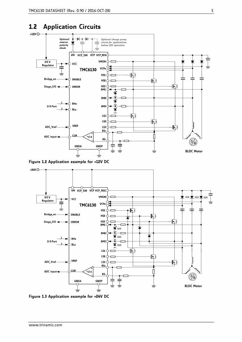
1.2 Application Circuits
TMC6130
VM VCP_SW VCP
VCC
ENABLE
ERROR
BHx
BLx
VREF
CUR
GNDPGNDA
RS+
RS-
LS1
LS2
LS3
HS1
HS2
HS3BM1
BM2
BM3
VCPx
VMON
VCP_REG
Diagn_I/O
Bridge_en
I/ 0 Port
3
3
ADC_Vref
ADC input
3/5 V Regulator
*17.2
BLDC Motor
NS
+12V
Optional reserve polarity diode
Optional charge pump circuit for applications below 12V operation
Figure 1.2 Application example for +12V DC
TMC6130
VM VCP_SW VCP
VCC
ENABLE
ERROR
BHx
BLx
VREF
CUR
GNDPGNDA
RS+
RS-
LS1
LS2
LS3
HS1
HS2
HS3BM1
BM2
BM3
VCPx
VMON
VCP_REG
Diagn_I/O
Bridge_en
I/ 0 Port
3
3
ADC_Vref
ADC input
3/5 V Regulator
*17.2
BLDC Motor
NS
+24V
R2R
R2R
R2R
R2R R2R R2R
Figure 1.3 Application example for +24V DC
TMC6130 DATASHEET (Rev. 0.90 / 2016-OCT-28) 6
www.trinamic.com
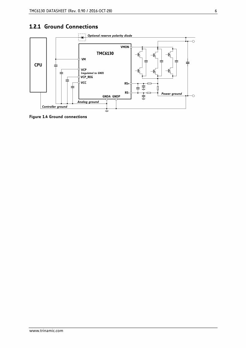
1.2.1 Ground Connections
RS+
VMON
VM
TMC6130
VCP(regulated to GND)
VCP_REG
VCC
GNDPGNDARS-
Analog ground
Controller ground
Optional reserve polarity diode
CPU
Power ground
Figure 1.4 Ground connections

TMC6130 DATASHEET (Rev. 0.90 / 2016-OCT-28) 7
www.trinamic.com
1.2.2 Pin Internal Connections
SUPPLY CONNECTIONS
55V
GNDP
VMON VM VCP_SWVCP
GNDP
55V
VCP_REG
GNDP
18.5V
VCC
GNDP
8V
GNDPGNDA
Figure 1.5 Supply connectinons
GATE DRIVER CONNECTIONS
VCPx
HSx
BMx
GNDP GNDP
LSx
VCP_REG
55V 18.5V
10V
Figure 1.6 Gate driver connections
DIGITAL IO CONNECTIONS
GNDP
BLx
VCC
GNDP
BHx
VCC
GNDP
ERROR
VCC
GNDP
ENABLE
18.5V
Figure 1.7 Digital IO connections
AMPLIFIER CONNECTIONS
RS-
RS+
VCC
CUR
VCCVCC VCC
VREF
Figure 1.8 Amplifier connections

TMC6130 DATASHEET (Rev. 0.90 / 2016-OCT-28) 8
www.trinamic.com
2 Pin Assignments
2.1 Package Outline
RS+
CURRENT
BL1
BL2
BL3
BM2
BH3
VM
ON
BM
3
VCP1
BM
1
HS1
VCP
VCP_REG
LS2
LS3
LS1
GNDP
VCP_SW
VM
VCP3
Top view
ERROR
ENABLE
32 31 30 29 28 27 26 25
9 10 11 12 13 14 15 16
1718
1920
2122
2324
12
34
56
78
TMC6130-LAHS3
VCP2
HS2
GNDA
BH2
BH1
VCC
VREF
RS-
Figure 2.1 TMC6130 pin assignments
2.2 Signal Descriptions Name Number Type Function
RS+ 1 Analog Current sensor input (positive)
CURRENT 2 Analog Current sensor output; diagnostic output in case of fault
BL1 3 Digital PWM input for low-side bridge n-FET1
BL2 4 Digital PWM input for low-side bridge n-FET2
BL3 5 Digital PWM input for low-side bridge n-FET3
ERROR 6 IO Diagnostic feedback IO
ENABLE 7 IO Enable input
BM2 8 Phase Motor phase 2
HS2 9 Output PWM output to high-side n-FET2 gate
VCP2 10 Supply Charge pump supply for high-side n-FET2
BM1 11 Phase Motor phase 1
HS1 12 Output PWM output to high side n-FET1 gate
VCP1 13 Supply Charge pump supply for high-side n-FET1
BM3 14 Phase Motor phase 3
HS3 15 Output PWM output to high side n-FET3 gate
VCP3 16 Supply Charge pump supply for high-side n-FET3
VCP 17 Analog Charge pump generated supply, unregulated
VCP_REG 18 Analog Regulated output from charge pump to drive n-FET gates
LS2 19 Output PWM output to low-side n-FET2 gate
LS3 20 Output PWM output to low-side n-FET3 gate
LS1 21 Output PWM output to low-side n-FET1 gate
GNDP 22 Ground Driver ground
VCP_SW 23 Analog Output of charge pump to boost low battery

TMC6130 DATASHEET (Rev. 0.90 / 2016-OCT-28) 9
www.trinamic.com
Name Number Type Function
VM 24 Supply Power supply input
VMON 25 Input Supply for 3 high-side n-FETs to monitor drain source voltage VDS
GNDA 26 Ground Analog ground
BH2 27 Digital PWM input for high-side n-FET2
BH1 28 Digital PWM input for high-side n-FET1
BH3 29 Digital PWM input for high-side n-FET3
VCC 30 Supply The input voltage on VCC is used to drive the digital IO’s, and is used to supply the shunt amplifier. Sleep mode control: VCC = 0V puts the pre-driver in sleep mode.
VREF 31 Analog Reference voltage input for current sense
RS- 32 Analog Current sensor input (negative)
Table 2.1 Pin definitions and descriptions

TMC6130 DATASHEET (Rev. 0.90 / 2016-OCT-28) 10
www.trinamic.com
3 Currents and Current Control
3.1 Supply Systems The current for operation of the system is supplied via VM and VCC. VCC supplies the IOs, and the amplifier. In case VCC is supplied with a limited output impedance (for instance from a microcontroller IO), the performance of the amplifier may be affected. VM supplies the internal operation and the charge pump. There are two possibilities to connect the boost current capacitor to the TMC6130. For charge pump mode 0 (default setting), connect it to VCP as shown in Figure 3.1.
CCP
VM VCP_SW VCP
CBOOST
+VBAT
CM
VCC
BHx
BLx
ENABLE
CURRENT
ERROR
+3.3V
VREGVCP_REG
VCPx
HSx
BMx
LSx
IDIODE_CPITOT
IM
IM_CP
IM_INT
ICC
ILOAD
Charge Pump Mode = 0
SLEEP
CCP
VM VCP_SW VCP
+VBAT
CM
VCC
BHx
BLx
ENABLE
CURRENT
ERROR
+3.3V
VREGVCP_REG
VCPx
HSx
BMx
LSx
IDIODE_CPITOT
IM
IM_CP
IM_INT
ICC
ILOAD
Charge Pump Mode = 1
SLEEP
CBOOST
*17.2 *17.2
Figure 3.1 Power supply systems: CPMODE = 0 and CPMODE = 1
STANDARD OPERATION: CHARGE PUMP MODE = 0
The standard operation of the charge pump is to ensure sufficient gate voltage to the bootstrap capacitors in case of low voltage conditions. VBOOST is regulated compared to GND level. The charge pump will not be switching when VM > VREG+2*VF with VF = forward voltage of charge pump diodes.
CHARGE PUMP MODE = 1 (has to be programmed and stored in EEPROM via SPI)
Alternatively, the charge pump can regulate VBOOST compared to VM. In this case the CBOOST capacitor should be connected to VM to ensure any supply variations are coupled to the VBOOST level. The disadvantage is an additional amount of dissipation inside the pre-driver to regulate VREG. The default configuration is stored in the integrated EEPROM. In case CPMODE1 is desired, it is necessary to change EEPROM configuration bits (using the SPI interface or via bit banging).

TMC6130 DATASHEET (Rev. 0.90 / 2016-OCT-28) 11
www.trinamic.com
3.2 100% PWM with Bootstrap A current is drawn from the VCP_SW pin to the phase pins. This current will discharge the gate voltage on top of any external pull down gate resistance.
CALCULATION EXAMPLE 1 CALCULATION EXAMPLE 2
Parameter Value Unit Parameter Value Unit
bootstrap 330 nF bootstrap 100 nF
VCP_reg 12 V VCP_reg 12 V
Qbootstr 3960 nC Qbootstr 1200 nC
QFET 200 nC QFET 120 nC
VGS_initial 11.4 V VGS_initial 10.9 V
Rcp_leak 0.75 MΩ Leakage 15 µA Leakage 15 µA
On time 60 ms On time 10 ms
Qleak 914 nC Qleak 152 nC
VGS_end 9.4 V VGS_end 9.8 V
VGS_drop 2.06 V VGS_drop 1.13 V
This gate leakage will limit the maximum state time during which 100% PWM can be applied.
3.3 Current Consumption in Sleep Mode Sleep mode is activated when the supply input VCC is pulled below VCC_SLEEP level. In sleep mode, the current consumption is reduced to ISSLEEP.
Pin Current consumption in Sleep Mode Input/Output
BHx
BLx
ENABLE
VREF
ERROR
Input pins, supplied from VCC GND
CURRENT Supplied from VCC GND
VCP_REG Supply regulator disabled GND
VCP Externally connected to supply. ~VBAT
VCP_SW Charge pump disabled. GND
VCPx Any charge that remains after VCP_REG is disabled will leak to ground.
GND
HSx
BMx
VM > 4.5V
In sleep mode, gate-discharge-resistors (RSGD) between HSx and BMx are activated.
GND
LSx VM > 4.5V
In sleep mode, gate-discharge-resistors (RSGD) between LSx and DGND are activated.
GND
ATTENTION!
In case input pins are externally pulled high while VCC is low, current will flow into VCC via internal protection diodes. This condition is not allowed! When VCC is pulled low, also ERROR will go low. This should not be interpreted as a diagnostic interrupt.

TMC6130 DATASHEET (Rev. 0.90 / 2016-OCT-28) 12
www.trinamic.com
STATES IN SLEEP MODE
Name Number Type State in Sleep Mode
RS+ 1 Analog GND
CUR 2 Analog GND (tied to VCC)
BL1 3 Digital GND (tied to VCC)
BL2 4 Digital GND (tied to VCC)
BL3 5 Digital GND (tied to VCC)
ERROR 6 IO GND (tied to VCC)
ENABLE 7 IO GND (tied to VCC)
BM2 8 Phase Connected via diode to GATE2
HS2 9 Output Internal pull down (RSGD) to GND
VCP2 10 Supply Any present charge leaks to GND
BM1 11 Phase Connected via Diode to GATE1
HS1 12 Output Internal pull down (RSGD) to GND
VCP1 13 Supply Any present charge leaks to GND
BM3 14 Phase Connected via Diode to GATE3
HS3 15 Output Internal pull down (RSGD) to GND
VCP3 16 Supply Any present charge leaks to GND
VCP 17 Analog Connected via charge pump diodes to VBAT
VCP_REG 18 Analog GND
LS2 19 Output Internal pull down (RSGD) to GND
LS3 20 Output Internal pull down (RSGD) to GND
LS1 21 Output Internal pull down (RSGD) to GND
GNDP 22 Ground Driver ground
VCP_SW 23 Analog GND
VM 24 Supply Power supply input
VMON 25 Input Connected to supply
GNDA 26 Ground Analog ground
BH2 27 Digital GND (tied to VCC)
BH1 28 Digital GND (tied to VCC)
BH3 29 Digital GND (tied to VCC)
VCC 30 Supply Externally pulled low
VREF 31 Analog GND
RS- 32 Analog GND

TMC6130 DATASHEET (Rev. 0.90 / 2016-OCT-28) 13
www.trinamic.com
4 Diagnostics
4.1 ERROR Interface ERROR is a serial interface that feeds back detailed diagnostics information to the microcontroller. Two modes for supplying diagnostic feedback can be used (configured in EEPROM). The default configuration for the TMC6130 is PWM_SPEED = 1. PWM_SPEED = 0 Slow response diagnostic mode
PWM period TERROR ≈ 64µs for frequency FERROR_S
PWM_SPEED = 1 Fast response diagnostic mode PWM period TERROR ≈ 10µs for frequency FERROR_F
In these modes detailed diagnostic information is provided in the form of a PWM duty cycle. Each error corresponds to one duty cycle. The duty cycle is transmitted until the microcontroller acknowledges the reception of the duty cycle. The microcontroller acknowledges by pulling the ERROR line low for a period tACK > tERROR.
T T T T T T T T T T T
ERROR 1 ERROR 2 ERROR 3 EOF
1 3 1 13 3
2 2 2
Tack Tack Tack TackMCU
1 MCU pulls ERROR low.2 TMC6130 detects acknowledge on falling edge.3 MCU releases ERROR line.
Figure 4.1 ERROR handshake protocol
At each falling edge the TMC6130 checks the actual voltage on the ERROR line to detect an acknowledgement. When an acknowledgement is detected the duty cycle value is changed to the corresponding duty cycle value of the highest priority next error that has not yet been transmitted. This sequence of capturing duty cycle and acknowledging continues until the end of the frame (EOF) duty cycle has been received. By acknowledging the EOF duty cycle all error latches are reset and the ERROR line goes high again until a new error occurs.
ATTENTION - It is possible that a lower priority error is transmitted before a higher priority error because the
higher priority error occurred after the start of transmission of the lower priority error.
- When VCC is pulled low to put the TMC6130 into sleep mode, ERROR will go low as well. As soon as VCC goes high, ERROR will go high as well and remains high: no EOF is required in this case.
- As long as the regulated voltages on VCP and VCP_REG have not been achieved, ERROR may immediately start to go in diagnostic mode. This implies the microcontroller has to acknowledge these errors until the undervoltage conditions have been resolved. As soon as ERROR no longer enters diagnostic mode, the pre-driver is ready for operation.

TMC6130 DATASHEET (Rev. 0.90 / 2016-OCT-28) 14
www.trinamic.com
ACKNOWLEDGE ON ERROR
For the CPU to acknowledge ERROR it should be able to keep the line low while ERROR is pulling the line high.
VCC
ERROR<5mA
<5mA
VCC
Microcontroller
CLOAD < 100pF
TMC6130
Figure 4.2 ERROR output
OVERVIEW DIAGNOSTIC ERRORS
Priority Input Error Code
Duty Cycle [%]
Debounce Time
Description
11 ERROR_EOF 93.5 n/a End of frame
10 VDS_ERR 82,5 2µs
Drain-source voltage Error = VDS_T1 || VDS_T2 || VDS_T3 || VDS_B1 || VDS_B2 || VDS_B3 Can be Masked by VDS_COMP_EN. To avoid erroneous triggering due to switching there is a programmable blanking time on top of the debounce time: VDS_BLANKTIME[1:0].
9 EEP_ERR 55 n/a EEPROM DED error
8 VCC_UV 49.5 8µs VCC undervoltage
7 VM_OV 44
2µs VM overvoltage. This event cannot be masked!
6 VM_UV 38.5 8µs VM undervoltage
5 OVT 33 2µs Overtemperature
4 VCP_REG_UV 27.5 16µs VCP_REG undervoltage
3 VGS_UV 22 2µs Gate-source undervoltage This event can be masked by setting VGS_UV_COMP_EN=0
2 VCP_UV 16.5 16µs VCP undervoltage
1 VCP_REG_OV 11 2µs Voltage regulator overvoltage This event can be masked by setting VREG_OV_BF_EN=0
NOTES
- In case of multiple errors at the same time, priority is defined: 0 is highest priority, 16 is lowest priority.
- Duty cycle is transmitting with 5 bits resolution.
- Since the rise and fall times are matched, the resulting error is depending on the input comparator level of the microcontroller. If the comparator level is at VCC/2, there is no error. In any other case there is a systematic error which can be taken into account.

TMC6130 DATASHEET (Rev. 0.90 / 2016-OCT-28) 15
www.trinamic.com
4.2 Hardware Protection Hardware protection refers to the capability of the microcontroller to turn off the TMC6130 pre-driver without intervention in case of error condition. All gate voltages have to be pulled low to Z-state. An overvoltage condition on VM will always switch off the pre-driver, in order to protect it. This safety feature cannot be masked.
4.2.1 VDS Overvoltage The reaction of the pre-driver on VDS (drain source voltage) overvoltage events can be configured in EEPROM with bridge feedback (BF) bits. Per default configuration, VDS_COMP_EN and VDS_BF_EN are set to 1. Thus, in case of VDS overvoltage, ERROR reports error and the pre-driver is enabled. For any other EEPROM configuration it is necessary to use the SPI interface or to communicate with the microcontroller via bit banging. Note, that in most cases it is not necessary to change EEPROM settings. Therefore, information about programming the EEPROM via SPI is subject of an application note and not mentioned here.
VDS_COMP_EN VDS_BF_EN Reaction
0 - Any possible drain source (VDS) overvoltage events are neglected: no reaction on ERROR line. Pre-driver remains active.
1 0 ERROR reports error and pre-driver remains active.
1 1 ERROR reports error and pre-driver is disabled.
4.2.2 VCP_REG Overvoltage The reaction of the pre-driver on VCP_REG overvoltage events can be configured in EEPROM with bridge feedback (BF) bits. The default configuration is VCP_REG_OV_BF_EN = 1. Thus, ERROR reports error and bridge driver is set in tri-state if the error flag VCP_REG_OV is set. For any other EEPROM configuration it is necessary to use the SPI interface or to communicate with the microcontroller via bit banging. Note, that in most cases it is not necessary to change EEPROM settings. Therefore, information about programming the EEPROM via SPI is subject of an application note and not mentioned here.
VCP_REG_OV_BF_EN Reaction
0 ERROR reports error.
1
ERROR reports error.
VCP_REG overvoltage bridge feedback is enabled: 1: When error flag VCP_REG_OV = 1 bridge driver is set in tri-state.
0: When error flag VCP_REG_OV = 1 no effect on bridge driver. This setting can be used to mask VCP_REG_OV event.
4.2.3 Pre-driver Output State Summary The table below shows all conditions due to which the pre-driver may be disabled.
Pre-driver disabled (Z-state) Pre-driver released again
As soon as an error condition appears for which the hardware protection is activated.
VM_OV VDS VCP_REG_OV
As soon as the end of frame EOF has been acknowledged.
As soon as VCC is low.
As soon as VCC is high.
As soon as ENABLE is low.
As soon as ENABLE is high.

TMC6130 DATASHEET (Rev. 0.90 / 2016-OCT-28) 16
www.trinamic.com
5 EEPROM Default Configuration A good pre-driver configuration is already done by TRINAMIC. The EEPROM features single error correction and double error detection.
EEPROM PROGRAMMING The EEPROM data can be programmed by the microcontroller via an SPI interface. In most cases it is not necessary to change EEPROM settings. Therefore, information about programming the EEPROM via SPI is subject of an application note and not mentioned here.
MEMORY MAP
SPI
Address
[2:0]
ED7 ED6 ED5 ED4 ED3 ED2 ED1 ED0
0 Res. Res. Res. Res. Res. Res. Res. Res.
1 Res. Res. Res. Res. Res. Res. Res. Res.
2 DEAD_TIME[2:0] VDSMON[2:0] CPMODE Res.
3 VDS_BLANK_TIME[1:0] PWM_SPEED Res. CUR_GAIN[2:0] Res.
4 VREG_OV_BF_EN
VDS_
BF_EN
VDS_
COMP_EN
VGS_UV_COMP_EN
0 EN_CP Res. Res.
5 SPI_EN 1 Res. Res. Res. Res. Res. Res.
EEPROM BITS
Bit name Description Default
Driver Configuration
DEAD_TIME[2:0] Defines the DEAD TIME between the HS FET and LS FET of the same phase. Default value: 1.0µs.
011
VDSMON[2:0] Defines the detection threshold level of the Vds monitoring. Default value: 2V.
111
VDS_BLANK_TIME
[1:0]
Defines the duration of the Vds monitor blanking time after the on-transition of the FET. Default value: 3.0 µs
10
CUR_GAIN[2:0] Defines the gain of the current sense amplifier.
Default value: *17.2
011
CPMODE 0: VBOOST voltage is regulated relative to ground
1: VBOOST voltage is regulated relative to VSUP.
0
IC Configuration
SPI_EN When set, the SPI block is enabled.
When reset, no SPI possible.
In SPI mode this value can only be programmed from 1 to 0, not from 0 to 1.
1
VCP_REG_OV_BF_EN VCP_REG Overvoltage bridge feedback enable 1: When VCP_REG_OV = 1 Bridge driver is SET in tri-state
0: When VCP_REG_OV = 1 No effect on Bridge driver.
1
VDS_BF_EN VDS bridge feedback enable 1: When VDS_ERR = 1 Bridge driver is SET in tri-state.
0: When VDS_ERR = 1 No effect on Bridge driver.
1
VDS_COMP_EN 1: VDS comparator enabled
0: VDS comparator disabled
1
VGS_UV_COMP_EN 1: gate-source undervoltage comparator enabled
0: gate-source undervoltage comparator disabled
0
PWM_SPEED 1: PWM = FERROR_F
0: PWM = FERROR_S (ERROR PWM frequency slow ≈ 12.5KHz.)
1
EN_CP 1: boost charge pump enabled 0: boost charge pump disabled
0
OUT_RESERVE_RG Undefined 0

TMC6130 DATASHEET (Rev. 0.90 / 2016-OCT-28) 17
www.trinamic.com
5.1 Basic Information for SPI Communication To communicate with the TMC6130 via SPI the motor has to be in standstill because of pin sharing. When the chip is in SPI mode the EEPROM is programmable and readable via the SPI port. The TMC6130 switches from normal mode to SPI mode if the following conditions are met:
- EN = 0
- ERROR:
Any pending errors have been acknowledged
All BHx = high
All BLx = low
A Low Level pulse is applied on ERROR between 256µs (2048 Tclk) and 512µs (4096 Tclk) )
The chip returns from SPI mode to normal mode when
- EN = 1. This means that any ongoing EEPROM writes will be completed and the EEPROM state machine will copy all EEPROM contents into registers. Then the chip will return to normal mode. During this time the ERROR pin will be kept low. When the TMC6130 comes out of power ON reset, after leaving SPI mode and returning to normal mode, the pre-driver will be blocked until the data have been copied to the registers. This assures that all chip parameters are set correctly.
It only makes sense for the CPU to call for SPI if all errors are clear and acknowledged.
TMC6130 DATASHEET (Rev. 0.90 / 2016-OCT-28) 18
www.trinamic.com
6 Sense Amplifier The sense amplifier offers very low input offset, and very fast settling times. The input range can be adjusted by applying a suitable voltage on the VREF pin, typically as a resistor divider on VCC. For the definition of VREF, the input offset, the current range, and the linear output range of the CURRENT pin should all be taken into account. Input signal: VIN = VISP – VISN Max. input offset: VOFFSET_MAX = VIS_IO_MAX + TRANGE * VIS_IO_TDRIFT
TRANGE = over the full temperature range
VISENSE = (VIN +/-VOFFSET) * ISGAIN + VREF has to be in the range [VISENSE_MIN, VISENSE_MAX]
IMIN = [(VISENSE_MIN – VREF) / ISGAIN + VOFFSET] / RSHUNT
IMAX = [(VISENSE_MAX – VREF) / ISGAIN - VOFFSET ] / RSHUNT
Symbol Parameter
VIS_IO Input offset voltage
VIS_IO_TDRIFT Input offset voltage thermal drift
ISGAIN Closed loop gain
VISENSE_MIN ISENSE output voltage range low
VISENSE_MAX ISENSE output voltage range high
VREF Reference voltage input
The table below shows the current input range for two resistive divider settings on VREF. 1. VREF = VCC/2 for a symmetrical input range 2. VREF = VCC/18 for a maximum current level, whilst ensuring it is possible to measure the input
offset before starting the motor (ISENSE_MIN > 0A).
For ease of calculation a max temperature offset drift of 1mV was added to the 5mV offset. From this follows that the maximum input offset is 6mV.
VCC 3.3 3.3 3(**) 3(**) 5 5 4.5(**) 4.5(**)
Visensemin 0.02 0.02 0.02 0.02 0.02 0.02 0.02 0.02
Visensemax 3.28 3.28 2.98 2.98 4.98 4.98 4.48 4.48
div 2 18 2 18 2 18 2 18
VREF 1.65 0.18 1.50 0.17 2.50 0.28 2.25 0.25
Voffset 0.006

TMC6130 DATASHEET (Rev. 0.90 / 2016-OCT-28) 19
www.trinamic.com
6.1 Sense Amplifier Current Ranges: Examples for 1MΩ Shunt ISENSE_MIN
Gain DIV2 DIV18 DIV2 DIV18 DIV2 DIV18 DIV2 DIV18
8 -198 -14.4 -179 -12 -304 -26.2 -273 -23
10.3 -152 -9.9 -138 -8 -235 -19.0 -211 -16
13.3 -117 -6.3 -105 -5 -180 -13.4 -162 -11
17.2 -89 -3.5 -80 -3 -138 -9.0 -124 -7
22.2 -67 -1.4 -61 -0.6 -106 -5.6 -94 -4
28.7 -51 0.3(*) -46 0.9(*) -80 -3.0 -72 -2
37.0 -38 1.6(*) -34 2.0(*) -61 -1.0 -54 0
47.8 -28 2.6(*) -25 3(*) -46 0.6 -41 1
- (*) Applying a GAIN of 28.7 or higher with DIV 18 for 3.3V does not allow the measure the input offset
- (**) examples taking a 10% supply variation into account.
ISENSE_MAX Gain DIV2 DIV18 DIV2 DIV18 DIV2 DIV18 DIV2 DIV18
8 198 381 179 346 304 582 273 523
10.3 152 295 138 267 235 451 211 405
13.3 117 227 105 206 180 348 162 312
17.2 89 174 80 158 138 267 124 240
22.2 67 133 61 121 106 206 94 185
28.7 51 102 46 92 80 158 72 141
37.0 38 78 34 70 61 121 54 108
47.8 28 59 25 53 46 92 41 82

TMC6130 DATASHEET (Rev. 0.90 / 2016-OCT-28) 20
www.trinamic.com
7 FET Driver Implementation
7.1 Normal Operation The top side FET drivers are bootstrapped drivers. Each of the six external FET transistors which have to be connected can be controlled directly via six digital inputs. The six external FET transistors (or three half bridges) can also be controlled using only three digital input signals. Therefore, proceed as follows:
- Connect the BHx to VCC.
- Control the 3 phases via the BLx inputs. In this mode of operation, the TMC6130 will automatically generate the programmed dead times.
The drain source voltage VDS as well as the gate voltage VGS are monitored to ensure fail safe operation. The FET gate outputs are all pulled low by pulling ENABLE low.
7.2 FET Driver during Sleep Mode In sleep mode, a gate discharge resistance (RSGD ~ 1KΩ) is activated. This ensures that the FET gates remain fully in OFF state. It is the responsibility of the microcontroller to ensure all gate voltages are low, for instance by setting the ENABLE input low, prior to switching to sleep mode.
VCP_REG
VCPx
BMx
LSx
RSGD
HSx
RSGD
TMC6130
Figure 7.1 Fet driver during sleep mode: BMx is kept low with HSx through the internal body diode of the TMC6130.

TMC6130 DATASHEET (Rev. 0.90 / 2016-OCT-28) 21
www.trinamic.com
8 Absolute Maximum Ratings The maximum ratings may not be exceeded under any circumstances. Operating the circuit at or near more than one maximum rating at a time for extended periods shall be avoided by application design. All voltages are referenced to ground (GND). Positive currents flow into the IC. The absolute maximum ratings given in the table below are limiting values that do not lead to a permanent damage of the device but exceeding any of these limits may do so. Long term exposure to limiting values may affect the reliability of the device. Reliable operation of the IC is only specified within the limits shown in the table.
Parameter Symbol Condition Min Max Unit
Supply voltage VM VMON
t < 200ms *1) -0.5 45 V
permanent (functional) -0.5 28 V
Voltage on analogue LV VAN_LV -0.5 VCC+0.5 V
Digital output voltage VOUT_DIG -0.5 VCC+0.5 V
Digital input voltage VIN_DIG -0.5 VCC+0.5 V
Digital input current IIN_DIG -10 10 mA
Input voltage on BMx pins VIN_BMx -2 45 V
Maximum latch–up free current at any pin
ILATCH according JEDEC JESD78, AEC-Q100-004
-100 100 mA
ESD capability of any other pin
ESD human body model *2) -2 +2 kV
Storage temperature tSTG -55 150 °C
Junction temperature tJ *3) -40 150 °C
Thermal resistance package RTHJA in free air on multilayer pcb (JEDEC 1s2p)
(37) to be confirmed
K/W
RTHJC referring to center of exposed pad
(10) to be confirmed
K/W
NOTES
*1) Only during load dump pulse. *2) Equivalent to discharging a 100pF capacitor through a 1.5kΩ resistor conform to MIL STD 883 method
3015.7 *3) For applications with tJ > 125C: the extended temperature range is only allowed for a limited period
of time. The application mission profile has to be agreed by TRINAMIC. Some analogue parameters may drift out of limits, but chip function is guaranteed.

TMC6130 DATASHEET (Rev. 0.90 / 2016-OCT-28) 22
www.trinamic.com
9 General Electrical Specifications
9.1 Operational Range (unless otherwise specified)
Parameter Symbol Min Max Unit
Application temperature tA -40 125 °C
Supply voltage TMC6130 VM 7 18 V
VCC logic supply input voltage VCC 3 5.5 V
BATTERY SUPPLY
Parameter Symbol Test Conditions Min Typ Max Units
Supply voltage VM 7 18 V
Supply voltage extended range low
VM_ERL Functional with relaxed specification.
4.5 7 V
Supply voltage extended range high
VM_ERH Functional with relaxed specification.
18 28 V
Quiescent current drawn from VM
IMSLEEP VCC = low 30 µA
Operating current drawn from VM
IM_INT Pre-driver operation without charge pump operation (EN_CP=0).
1 mA
Battery overvoltage threshold high
VM_OVH Warning on ERROR. 35 V
Battery overvoltage threshold low
VM_OVL ERROR released. 31 V
Battery overvoltage threshold hyst
VM_OV_HY 0.4 1 V
Battery overvoltage debounce time
VM_OV_DEB 2 µS
Battery undervoltage threshold high
VM_UVH Warning on ERROR. 6 V
Battery undervoltage threshold low
VM_UVL ERROR released. 5 V
Battery undervoltage threshold hyst
VM_UVHY 0.2 0.5 V
Battery undervoltage debounce time
VM_UV_DEB 10 µS
Power on reset level VPOR Reset released on rising edge of VM while VCC is high.
3 4.5 V

TMC6130 DATASHEET (Rev. 0.90 / 2016-OCT-28) 23
www.trinamic.com
POWER AND TEMPERATURE
Parameter Symbol Test Conditions Min Typ Max Units
Overtemperature protection high
OTH Warning on ERROR. 153 166 183 C
Overtemperature protection low
OTL ERROR released. 123 137 153 C
VCC IO SUPPLY INPUT
Parameter Symbol Test Conditions Min Typ Max Units
VCC operating current ICC Maximum input current includes ERROR current sourcing.
20 mA
VCC pull down resistance
VCC_RPD 230 300 370 KΩ
VCC input voltage VCC VCC = 3.3V or 5V, logic supply.
3 5.5 V
VCC input undervoltage high 1)
VCC_UV_H
VCC increasing, NFET control is activated.
2.7 2.8 V
VCC input undervoltage low
VCC_UV_L VCC decreasing, disable NFET control.
2.6 2.7 V
VCC input undervoltage hyst
VCC_UV_HY 0.07 0.1 V
VCC sleep voltage high VCC_SLEEP_H VCC increasing, out of sleep.
2.45 2.6 V
VCC sleep voltage low VCC_SLEEP_L VCC decreasing, go to sleep.
1.9 2 V
VCC sleep voltage hyst VCC_SLEEP_HY 0.45 0.58 V
1) The info VCC_UV_X is used to disable the control of the external FETs.
ON-CHIP OSCILLATOR
Parameter Symbol Test Conditions Min Typ Max Units
Charge pump frequency
FCP 170 230 KHz
ERROR PWM frequency fast
FERROR_F 85 115 KHz
ERROR PWM frequency slow
FERROR_S 10.6 14.4 KHz
SPI start up pulse duration
tSPI_SU EN = Low BH1/2/3 = low BL1/2/3 = high
2048/FOSC
4096/FOSC
Sec
TMC6130 DATASHEET (Rev. 0.90 / 2016-OCT-28) 24
www.trinamic.com
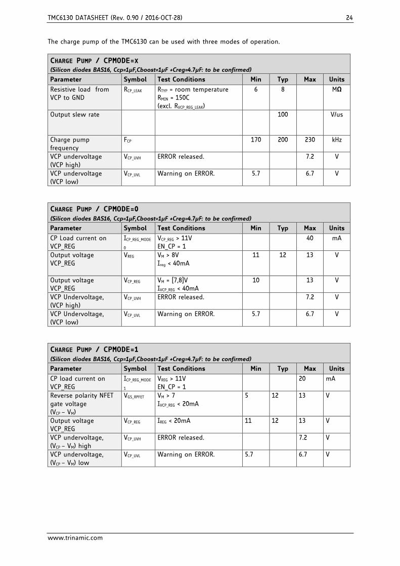
The charge pump of the TMC6130 can be used with three modes of operation.
CHARGE PUMP / CPMODE=X (Silicon diodes BAS16, Ccp=1µF,Cboost=1µF +Creg=4.7µF: to be confirmed)
Parameter Symbol Test Conditions Min Typ Max Units
Resistive load from VCP to GND
RCP_LEAK RTYP = room temperature RMIN = 150C (excl. RVCP_REG_LEAK)
6 8 MΩ
Output slew rate
100 V/us
Charge pump frequency
FCP
170 200 230 kHz
VCP undervoltage (VCP high)
VCP_UVH ERROR released. 7.2 V
VCP undervoltage (VCP low)
VCP_UVL Warning on ERROR. 5.7 6.7 V
CHARGE PUMP / CPMODE=0 (Silicon diodes BAS16, Ccp=1µF,Cboost=1µF +Creg=4.7µF: to be confirmed)
Parameter Symbol Test Conditions Min Typ Max Units
CP Load current on VCP_REG
ICP_REG_MODE
0 VCP_REG > 11V EN_CP = 1
40 mA
Output voltage VCP_REG
VREG VM > 8V Ireg < 40mA
11 12 13 V
Output voltage VCP_REG
VCP_REG VM = [7,8]V IVCP_REG < 40mA
10 13 V
VCP Undervoltage, (VCP high)
VCP_UVH ERROR released. 7.2 V
VCP Undervoltage, (VCP low)
VCP_UVL Warning on ERROR. 5.7 6.7 V
CHARGE PUMP / CPMODE=1 (Silicon diodes BAS16, Ccp=1µF,Cboost=1µF +Creg=4.7µF: to be confirmed)
Parameter Symbol Test Conditions Min Typ Max Units
CP load current on VCP_REG
ICP_REG_MODE
1 VREG > 11V EN_CP = 1
20 mA
Reverse polarity NFET gate voltage (VCP – VM)
VGS_RPFET VM > 7 IVCP_REG < 20mA
5 12 13 V
Output voltage VCP_REG
VCP_REG IREG < 20mA 11 12 13 V
VCP undervoltage, (VCP – VM) high
VCP_UVH ERROR released. 7.2 V
VCP undervoltage, (VCP – VM) low
VCP_UVL Warning on ERROR. 5.7 6.7 V

TMC6130 DATASHEET (Rev. 0.90 / 2016-OCT-28) 25
www.trinamic.com
VREG Warnings / CPMODE=X
Parameter Symbol Test Conditions Min Typ Max Units
Internal resistive load from VCP_REG to GND
RVCP_REG_LEAK RTYP = Room RMIN = 150C
0.3 0.4 MΩ
VCP_REG overvoltage high
VCP_REG_OVH Warning on ERROR. 14.2 16.5 V
VCP_REG overvoltage low
VCP_REG_OVL ERROR released. 13.5 V
VCP_REG overvoltage hyst
VCP_REG_OVHY 0.7 1 V
VCP_REG undervoltage high
VCP_REG_UVH ERROR released.
8.1 V
VCP_REG undervoltage low
VCP_REG_UVL Warning on ERROR. 6.9 7.8 V
VBATF
Parameter Symbol Test Conditions Min Typ Max Units
Internal leakage from VMON to GND
RVMON_LEAK Pre-driver is not in sleep mode.
20 µA
FET GATE DRIVERS
Parameter Symbol Test Conditions Min Typ Max Units
Driver ON resistance2) RDR_ON 4 8 Ω
Rise time tR Cload = 1nF, 20% to 80% 6 7 15 ns
Fall time tF Cload = 1nF, 80% to 20% 4 7 15 ns
Pull-up on resistance RON_UP -10mA tJ = -40 -10mA, tJ = 150
2.4 6.5 Ω
Pull down on resistance
RON_DN 10mA tJ = -40 10mA, tJ = 150
1.5
5.7 Ω
Turn on gate drive peak current
IG_ON VGS = 0V -1 -1.4 A
Turn off gate drive peak current
IG_OFF VGS = 12V 1 1.6 A
Propagation delay tPD_DRV From logic input threshold to 2V VGS drive output at no load.
20 100 ns
Propagation delay matching
tPD_DRVM Transitions at the different phases at no load condition.
-20 20 ns
Programmable dead time : asynchronous internal delay between top and bottom FET
tDEAD DEAD_TIME[2:0] = 000 001 010 011 100 101 110 111
0.0001
0 0.5 0.75 1.0 1.5 2.0 3.0 6.0
0.0002
µs
Dead time tolerance tDEAD_TOL -15 15 %

TMC6130 DATASHEET (Rev. 0.90 / 2016-OCT-28) 26
www.trinamic.com
FET GATE DRIVERS
Parameter Symbol Test Conditions Min Typ Max Units
Programmable VDS monitor voltage
VDS_MON VDSMON[2:0] = 000: disabled
001 010 011 100 101 110 111
0.4 0.6 0.85 1.05 1.25 1.5 1.70
0.5 0.75 1.00 1.25 1.50 1.75 2.00
0.6 0.9 1.15 1.45 1.75 2.00 2.3
V
Programmable VDS monitor blanking time: internal delay between GATE signal high and enabling the corresponding VDS monitor
tVDS_BL VDS_BLANK_TIME[1:0] = 00 01 10 11
0.75 1.5 3 6
µs
VDS blanking time tolerance
tVDS_TOL -15 15 %
Sleep gate discharge resistor
RSGD Internal resistance between FET gate-source pins to switch-off FET. VCC = 0V (sleep mode) VGS = 0.5V See chapter FET driver during sleep mode.
1 KΩ
VGS under voltage monitor
VGS_UV Warning on ERROR. TBD 75 %VREG
PWM frequency FPWM 5 20 100 KHz
Leakage from VCPx to BMx
RCP_LEAK Typ = Room Min = 150C
0.75 1 MΩ
2) The driver on resistance is <5Ω at 25C. Maximum values correspond with 150C.
Logic IO (FET inputs, EN input)
Parameter Symbol Test Conditions Min Typ Max Units
Digital input high voltage
VIN_DIG_H Minimum voltage for input to be treated as logical high
70 %VCC
Digital input low voltage
VIN_DIG_L Maximum voltage for input to be treated as logical low
30 %VCC
Input pull-up resistance
RIN_DIG_PU BL1, BL2, BL3 90 410 KΩ
Input pull-down resistance
RIN_DIG_PD BH1, BH2, BH3 90 410 KΩ
Input pull-down resistance
REN_PD ENABLE 90 410 KΩ
SPI TIMING
Parameter Symbol Test Conditions Min Typ Max Units
SPI initial setup time tSPI_ISU 2 µsec
SPI clock frequency FSPI 500 KHz

TMC6130 DATASHEET (Rev. 0.90 / 2016-OCT-28) 27
www.trinamic.com
SPI TIMING
Parameter Symbol Test Conditions Min Typ Max Units
Rise/fall times tSPI_RF All rise/fall times on CLK, CSB, MISO, MOSI
200 nsec
CSB setup time tCSB_SU 1 µsec
CSB high time tCSB_H 2 µsec
Clock high time tCLK_H 1 µsec
Clock low time tCLK_L 1 µsec
Data in setup time tDI_SU 1 µsec
Data in hold time tDI_H 500 µsec
Data out ready delay tDO_R Cload at BL1<50pF 500 µsec
EEPROM read delay tEE_RD EE_RD = 1 6 µsec
EEPROM write delay tEE_WR EE_RD = 1 12 msec
ERROR OUTPUT
Parameter Symbol Test Conditions Min Typ Max Units
Pull-up current IERROR_PU VERROR = 0V -2.23 -5 mA
Pull-down current IERROR_PD VERROR = VCC 5 2.6 mA
ENABLE INPUT
Parameter Symbol Test Conditions Min Typ Max Units
Bridge disable propagation delay
ENPR_DEL From bridge enable EN< 0.2*VCC to VGS<0.5V with Cload=1nF.
1 µs

TMC6130 DATASHEET (Rev. 0.90 / 2016-OCT-28) 28
www.trinamic.com
CURRENT SENSE AMPLIFIER
Parameter Symbol Test Conditions Min Typ Max Units
Input offset voltage VIS_IO Input diff. voltage within +/-100mV; common mode within -0.5… 1.0V.
-5 5 mV
Input offset voltage thermal drift
VIS_IO_TDRIFT Input diff. voltage within +/-100mV; common mode within -0.5… 1.0V.
-10 10 µV/C
Input common mode rejection DC
ISCMR_DC Input diff. voltage within +/-100mV; common mode within -0.5… 1.0V.
60 dB
Input common mode rejection 1MHz
ISCMRR_AC Input diff. voltage within +/-100mV; common mode within -0.5… 1.0V.
40 dB
Input power supply rejection DC for VCC supply
ISPSRR_DC Input diff. voltage within +/-100mV; common mode within -0.5… 1.0V
60 dB
Input power supply rejection 1MHz for VCC supply
ISPSRR_AC Input diff. voltage within +/-100mV; common mode within -0.5… 1.0V.
40 dB
Closed loop gain ISGAIN Gain is programmable in EEPROM.
-3% 8.0 10.3 13.3 17.2 22.2 28.7 37.0 47.8
+3% -
Output settling time ISSET Amplified output to 99% of final value after input change.
1.0 µs
Output voltage range high
VCURRENT_MAX Current sense output max level.
VCC -0.020
VCC V
Output voltage range low
VCURRENT_MIN Current sense output min level.
GND GND +0.020
V
Output short circuit current to ground
ICURRENT_SC Output current saturation level.
1.4 mA
GBW ISGBW 10 MHz
Output slew rate ISSR 40 V/µs
CM spike recovery ISCM_REC CM spike = ± 1.5V duration = 250nsec
730 nS
VREF voltage input VREF 0 50 %VCC
TMC6130 DATASHEET (Rev. 0.90 / 2016-OCT-28) 29
www.trinamic.com
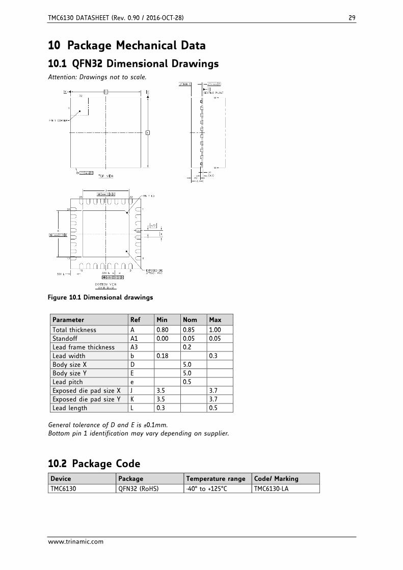
10 Package Mechanical Data
10.1 QFN32 Dimensional Drawings Attention: Drawings not to scale.
Parameter Ref Min Nom Max
Total thickness A 0.80 0.85 1.00
Standoff A1 0.00 0.05 0.05
Lead frame thickness A3 0.2
Lead width b 0.18 0.3
Body size X D 5.0
Body size Y E 5.0
Lead pitch e 0.5
Exposed die pad size X J 3.5 3.7
Exposed die pad size Y K 3.5 3.7
Lead length L 0.3 0.5
General tolerance of D and E is ±0.1mm. Bottom pin 1 identification may vary depending on supplier.
10.2 Package Code
Device Package Temperature range Code/ Marking
TMC6130 QFN32 (RoHS) -40° to +125°C TMC6130-LA
Figure 10.1 Dimensional drawings

TMC6130 DATASHEET (Rev. 0.90 / 2016-OCT-28) 30
www.trinamic.com
11 Disclaimer TRINAMIC Motion Control GmbH & Co. KG does not authorize or warrant any of its products for use in life support systems, without the specific written consent of TRINAMIC Motion Control GmbH & Co. KG. Life support systems are equipment intended to support or sustain life, and whose failure to perform, when properly used in accordance with instructions provided, can be reasonably expected to result in personal injury or death. Information given in this data sheet is believed to be accurate and reliable. However no responsibility is assumed for the consequences of its use nor for any infringement of patents or other rights of third parties which may result from its use. Specifications are subject to change without notice. All trademarks used are property of their respective owners.
12 ESD Sensitive Device The TMC6130 is an ESD-sensitive CMOS device and sensitive to electrostatic discharge. Take special care to use adequate grounding of personnel and machines in manual handling. After soldering the devices to the board, ESD requirements are more relaxed. Failure to do so can result in defects or decreased reliability.
Note: In a modern SMD manufacturing process, ESD voltages well below 100V are standard. A major source for ESD is hot-plugging the motor during operation. As the power MOSFETs are discrete devices, the device in fact is very rugged concerning any ESD event on the motor outputs. All other connections are typically protected due to external circuitry on the PCB.
TMC6130 DATASHEET (Rev. 0.90 / 2016-OCT-28) 31
www.trinamic.com
13 Table of Figures Figure 1.1 Block diagram and principle operation circuit ......................................................................................... 4 Figure 1.2 Application example for +12V DC ................................................................................................................. 5 Figure 1.3 Application example for +24V DC ................................................................................................................. 5 Figure 1.4 Ground connections ......................................................................................................................................... 6 Figure 1.5 Supply connectinons ....................................................................................................................................... 7 Figure 1.6 Gate driver connections .................................................................................................................................. 7 Figure 1.7 Digital IO connections .................................................................................................................................... 7 Figure 1.8 Amplifier connections ..................................................................................................................................... 7 Figure 2.1 TMC6130 pin assignments .............................................................................................................................. 8 Figure 3.1 Power supply systems: CPMODE = 0 and CPMODE = 1 ........................................................................ 10 Figure 4.1 ERROR handshake protocol .......................................................................................................................... 13 Figure 4.2 ERROR output ................................................................................................................................................... 14 Figure 7.1 Fet driver during sleep mode: BMx is kept low with HSx through the internal body diode of the TMC6130. ........................................................................................................................................................................ 20 Figure 10.1 Dimensional drawings ................................................................................................................................ 29

TMC6130 DATASHEET (Rev. 0.90 / 2016-OCT-28) 32
www.trinamic.com
14 Revision History
Version Date Author Description
0.9 2014-MAR-10 SD Initial version; preliminary.
1.0 2016-OCT-28 SK VDS_ERR error code in error code table corrected. Preliminary state removed.
15 References [TMC6130-EVAL] TMC6130-EVAL Manual Please refer to our web page http://www.trinamic.com.