tm57pa20/ pa20a/ pa40 8-bit microcontroller data sheet · 2018. 8. 10. · tm57pa20/20a/20b/...
TRANSCRIPT

TM57PA20/20A/20B/
20E/40/40E
DATA SHEET
Rev 3.0
tenx reserves the right to change or discontinue the manual and online documentation to this product herein to improve
reliability, function or design without further notice. Tenx does not assume any liability arising out of the application or use of
any product or circuit described herein; neither does it convey any license under its patent rights nor the rights of others. Tenx
products are not designed, intended, or authorized for use in life support appliances, devices, or systems. If Buyer purchases or
uses tenx products for any such unintended or unauthorized application, Buyer shall indemnify and hold tenx and its officers,
employees, subsidiaries, affiliates and distributors harmless against all claims, cost, damages, and expenses, and reasonable
attorney fees arising out of, directly or indirectly, any claim of personal injury or death associated with such unintended or
unauthorized use even if such claim alleges that tenx was negligent regarding the design or manufacture of the part.
TM57PA20/20A/20B/20E/40/40E Data Sheet
DS-TM57PA20_20A_20B_20E_40_40E_E 2 Rev 3.0, 2018/08/10
AMENDMENT HISTORY
Version Date Description
V2.0 Jan, 2012
1. Add the Electrical Characteristics specs in the Features section.
2. Add description in Reset section.
3. Merge the information about LVR Circuit Characteristics into
DC Characteristics table.
4. Modify Ordering Information table.
V2.1 Feb, 2012 1. Modify the description about LVR in Features section.
2. Revise the ROM modification in Features section.
V2.2 Jul, 2012 Modify Electrical Characteristics.
V2.3 Oct, 2012
1. Add TM57PA20A body related description
2. SYSCFG table & description for TM57PA20A
3. Add DC Characteristics for TM57PA20A
V2.4 Apr, 2013 1. Modify Block Diagram.
2. Modify Packaging Information.
V2.5 Jun, 2013 Add Pin Summary.
V2.6 Aug, 2013 Modify Ordering Information
V2.7 Nov, 2013 Modify PA20A PROM range
V2.8 Nov, 2014 1. Add PA20B information
2. Modify comparsion table
V2.9 Dec, 2015
1. Add PA20E/ PA40E body information
2. Add Comparsion Table (p7)
3. Add instruction cycles (p12)
4. Add Vdd=5.0, LVR3.1 is suitable (p16)
5. Add LVR & Temp curve (p52)
V3.0 Aug, 2018 1. Remove LVR2.1 (p5,p15,p16,p49)
TM57PA20/20A/20B/20E/40/40E Data Sheet
DS-TM57PA20_20A_20B_20E_40_40E_E 3 Rev 3.0, 2018/08/10
CONTENTS
AMENDMENT HISTORY ......................................................................................................... 2
FEATURES .................................................................................................................................. 5
BLOCK DIAGRAM .................................................................................................................... 7
PIN ASSIGNMENT ..................................................................................................................... 8
PIN DESCRIPTION .................................................................................................................... 9
PIN SUMMARY ......................................................................................................................... 10
FUNCTIONAL DESCRIPTION .............................................................................................. 11
1. CPU Core .......................................................................................................................... 11
1.1 Clock Scheme and Instruction Cycle ............................................................................. 11 1.2 Addressing Mode ........................................................................................................... 12 1.3 Programming Counter (PC) and Stack ........................................................................... 12 1.4 ALU and Working (W) Register .................................................................................... 13 1.5 STATUS Register .......................................................................................................... 13 1.6 Interrupt .......................................................................................................................... 14
2. Chip Operation Mode ...................................................................................................... 15
2.1 Reset ............................................................................................................................... 15 2.2 System Configuration Register (SYSCFG) ................................................................... 16 2.3 PROM Re-use ................................................................................................................ 17 1.4 Power-Down Mode ........................................................................................................ 17
3. Peripheral Functional Block ........................................................................................... 18
1.1 Watchdog (WDT) / Wakeup (WKT) Timer ................................................................... 18 3.2 Timer0: 8-bit Timer/Counter with Pre-scale (PSC) ....................................................... 19 3.3 Timer1: 8-bit Timer with Pre-scale (PSC) ..................................................................... 20 3.4 8+2 bit PWM .................................................................................................................. 22 3.5 12-bit ADC ..................................................................................................................... 24 3.6 System Clock Oscillator ................................................................................................. 26 3.7 BUZZER Output ............................................................................................................ 27
4. I/O Port.............................................................................................................................. 29
4.1 PA0-2 ............................................................................................................................. 29 4.2 PA3-6, PB0-1, PD0-7 ..................................................................................................... 30 4.3 PA7 ................................................................................................................................. 31
MEMORY MAP ......................................................................................................................... 32
F-Plane .................................................................................................................................... 32
R-Plane .................................................................................................................................... 34
INSTRUCTION SET ................................................................................................................. 36
TM57PA20/20A/20B/20E/40/40E Data Sheet
DS-TM57PA20_20A_20B_20E_40_40E_E 4 Rev 3.0, 2018/08/10
ELECTRICAL CHARACTERISTICS ................................................................................... 48
1. Absolute Maximum Ratings ............................................................................................ 48
2. DC Characteristics ........................................................................................................... 49
3. Clock Timing .................................................................................................................... 50
4. Reset Timing Characteristics .......................................................................................... 50
5. ADC Electrical Characteristics ....................................................................................... 50
PACKAGING INFORMATION .............................................................................................. 52
16-DIP Package Dimension ................................................................................................... 53
16-SOP Package Dimension .................................................................................................. 54
20-DIP Package Dimension ................................................................................................... 55
20-SOP Package Dimension .................................................................................................. 56

TM57PA20/20A/20B/20E/40/40E Data Sheet
DS-TM57PA20_20A_20B_20E_40_40E_E 5 Rev 3.0, 2018/08/10
FEATURES
1. ROM:
TM57PA20/20A/20B/20E: 2K x 14 bits OTP
TM57PA40/40E: 4K x 14 bits OTP or 2K x 14 bits TTP™ (Two Time Programmable ROM)
2. RAM: 184 x 8 bits
3. STACK: 6 Levels
4. I/O ports: Three Programmable I/O ports (Max. 18 pins)
5. Timer0/Counter: 8-bit timer/counter with divided by 1~256 pre-scale option
6. Timer1: 8-bit auto-reloadable timer with divided by 1~256 pre-scale option
7. Two 8+2 bit PWM channels capable of 1024 duty resolution
8. 12-bit ADC with 8 channel input
9. Buzzer output
10. Watchdog/Wakeup Timer: On chip Timer based on internal RC oscillation, 13~140 ms wakeup
time
11. Reset: Power On Reset, Watchdog Reset, Low Voltage Reset, External pin Reset
12. System Clock Mode:
(1) Slow Crystal: 32 KHz
(2) Fast Crystal: 455 KHz ~24 MHz
(3) Internal RC: 4 MHz
(4) External RC
13. 2-Level Low Voltage Reset: 3.1V
14. Operation Voltage: Low Voltage Reset Level to 5.5V
(1) fosc = 4 MHz, 2.4V ~ 5.5V
(2) fosc = 8 MHz, 2.4V ~ 5.5V
(3) fosc = 12 MHz, 2.8V ~ 5.5V
(4) fosc = 16 MHz, 3.0V ~ 5.5V
15. Instruction set: 36 Instructions
16. Interrupts: Three pin interrupts, Timer0/Timer1 interrupt and Wakeup Timer interrupt
17. Power Down mode support

TM57PA20/20A/20B/20E/40/40E Data Sheet
DS-TM57PA20_20A_20B_20E_40_40E_E 6 Rev 3.0, 2018/08/10
19. Package Types: 16-DIP/SOP, 20-DIP/SOP
20. Supported EV board on ICE
EV board: EV2795
TM57PA40/40E/20/20A/20B/20E comparsion Table:
TM57PA40 TM57PA40E - -
ROM 4K 4K - -
ROM usable range 0x000~0xFFB 0x000~0xFFB - -
TTPTM
O O - -
EFT immunity + ++ - -
ESD enhancement + ++ - -
Vih Typ. @5V (PA7) 2.8v 2.8v - -
Vil Typ. @5V (PA7) 1.8v 1.8v - -
RP Typ. @5V (PA7) 15Kohm 15Kohm - -
DC Characteristics Other unspecified items, refer to the DC characteristics for more details.
X: Not supported.
TM57PA20 TM57PA20E TM57PA20A TM57PA20B
ROM 2K 2K 2K 2K
ROM usable range 0x000~0x7FF 0x000~0x7FF 0x000~0x7FB 0x000~0x7FB
TTPTM
X X X X
EFT immunity + ++ + ++
ESD enhancement + ++ + ++
Vih Typ. @5V (PA7) 2.8v 2.8v 3.1v 2.9v
Vil Typ. @5V (PA7) 1.8v 1.8v 1.5v 1.6v
RP Typ. @5V (PA7) 15Kohm 15Kohm 60Kohm 60Kohm
DC Characteristics Other unspecified items, refer to the DC characteristics for more details.
X: not support
++ is better than +

TM57PA20/20A/20B/20E/40/40E Data Sheet
DS-TM57PA20_20A_20B_20E_40_40E_E 7 Rev 3.0, 2018/08/10
BLOCK DIAGRAM
Clock Generator
TM57PA20/20A/20B/20E/40/40E Block Diagram
4/2K OTP ROM
FXT/SXT
PA0~PA6
nRESET
ADC
Port A
Reset
VSS
8-bit
RISC core
VDD VPP
184BSRAM
Timer0
Timer1
WKT
WDT
LVR
INT0~INT1Interrupt
PB0~PB1Port B
PD0~PD7Port D
XRC
IRC
ADC0~ADC7
PWMPWM0
BuzzerBuzzer
PWM1
PA7
TM57PA20/20A/20B/20E/40/40E Data Sheet
DS-TM57PA20_20A_20B_20E_40_40E_E 8 Rev 3.0, 2018/08/10
PIN ASSIGNMENT
VSS
Xrc/Xin/PA4
Xout/PA3
VPP/nRESET/ INT2/PA7
T1OUT/PD0
BUZZER/PD1
PD2
PD3
TM57PA20
TM57PA20A
TM57PA20B
TM57PA40
DIP-16
SOP-16
1
2
3
4
5
6
7
8
VDD
PA6/ADC0/INT0
PA1/ADC1/INT1
PA2/ADC2/T0I
PB1/ADC3
PD7/ADC4
PA5/ADC5
PA0/PWM0
16
15
14
13
12
11
10
9
VSS
Xrc/Xin/PA4
Xout/PA3
VPP/nRESET/INT2/PA7
T1OUT/PD0
BUZZER/PD1
PD2
PD3
PD4
PD5
TM57PA20
TM57PA20A
TM57PA20B
TM57PA40
DIP-20
SOP-20
1
2
3
4
5
6
7
8
9
10
VDD
PA6/ADC0/INT0
PA1/ADC1/INT1
PA2/ADC2/T0I
PB1/ADC3
PD7/ADC4
PA5/ADC5
PA0/PWM0
PB0/ADC7/PWM1
PD6/ADC6/TCOUT
20
19
18
17
16
15
14
13
12
11

TM57PA20/20A/20B/20E/40/40E Data Sheet
DS-TM57PA20_20A_20B_20E_40_40E_E 9 Rev 3.0, 2018/08/10
PIN DESCRIPTION
Name In/Out Pin Description
PA2–PA0 I/O Bit-programmable I/O port for Schmitt-trigger input, CMOS “push-pull” output or
“pseudo-open-drain” output. Pull-up resistors are assignable by software.
PA6-PA3
PB1-PB0
PD7-PD0
I/O Bit-programmable I/O port for Schmitt-trigger input, CMOS “push-pull” output or
“open-drain” output. Pull-up resistors are assignable by software.
PA7 I Schmitt-trigger input
nRESET I External active low reset
Xin, Xout – Crystal/Resonator oscillator connection for system clock
Xrc External RC oscillator connection for system clock
VDD, VSS P Power input pin and ground
VPP I PROM programming high voltage input
INT0~2 I External interrupt input
T0I I Timer0’s input in counter mode
T1OUT O Timer1 match output, T1OUT toggles when Timer1 overflow occurs
BUZZER O BUZZER output
TCOUT O Instruction cycle clock divided by N output. Where N is 1,2,4,8. The instruction
clock frequency is system clock frequency divided by two.
PWM0/PWM1 O 10-bit PWM output
ADC7~0 I A/D converter input
TM57PA20/20A/20B/20E/40/40E Data Sheet
DS-TM57PA20_20A_20B_20E_40_40E_E 10 Rev 3.0, 2018/08/10
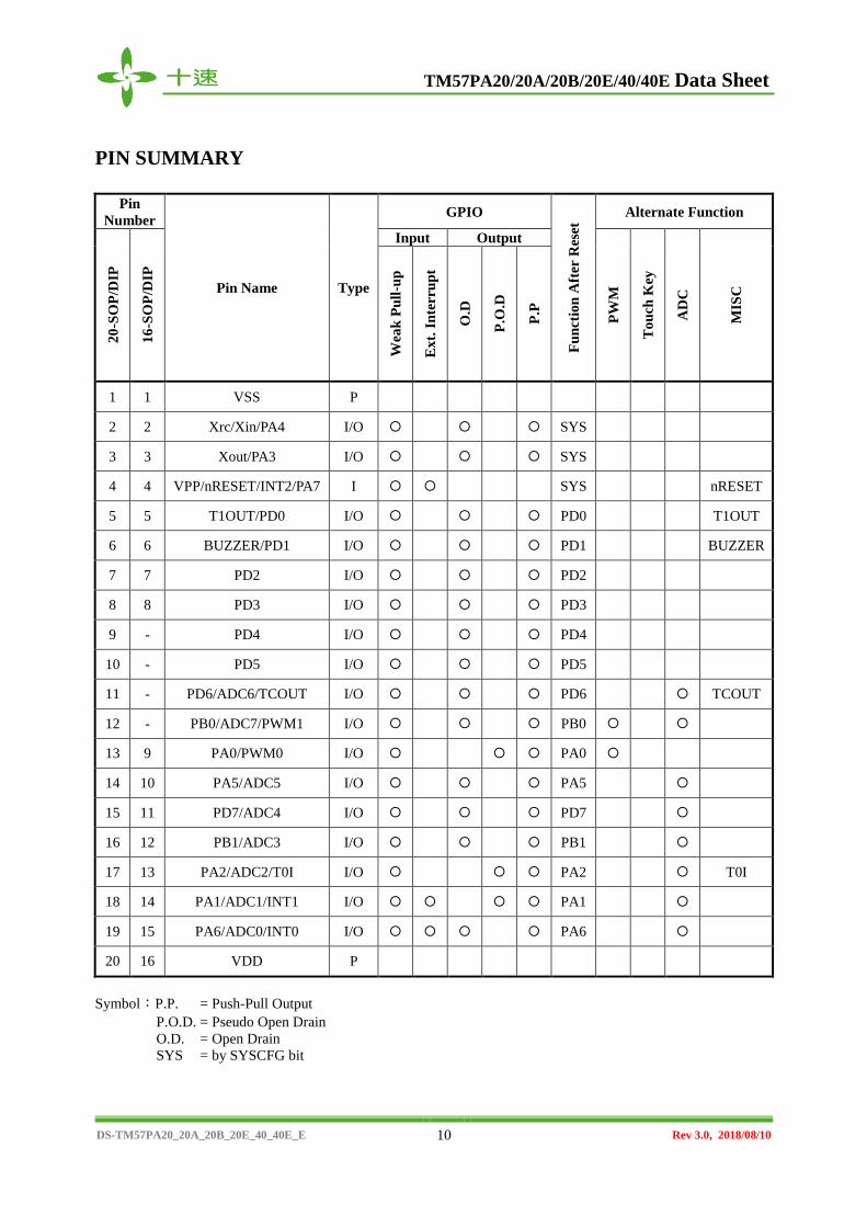
PIN SUMMARY
Pin
Number
Pin Name Type
GPIO
Fu
nct
ion
Aft
er R
eset
Alternate Function
20
-SO
P/D
IP
16
-SO
P/D
IP
Input Output
PW
M
To
uch
Key
AD
C
MIS
C
Wea
k P
ull
-up
Ex
t. I
nte
rru
pt
O.D
P.O
.D
P.P
1 1 VSS P
2 2 Xrc/Xin/PA4 I/O SYS
3 3 Xout/PA3 I/O SYS
4 4 VPP/nRESET/INT2/PA7 I SYS nRESET
5 5 T1OUT/PD0 I/O PD0 T1OUT
6 6 BUZZER/PD1 I/O PD1 BUZZER
7 7 PD2 I/O PD2
8 8 PD3 I/O PD3
9 - PD4 I/O PD4
10 - PD5 I/O PD5
11 - PD6/ADC6/TCOUT I/O PD6 TCOUT
12 - PB0/ADC7/PWM1 I/O PB0
13 9 PA0/PWM0 I/O PA0
14 10 PA5/ADC5 I/O PA5
15 11 PD7/ADC4 I/O PD7
16 12 PB1/ADC3 I/O PB1
17 13 PA2/ADC2/T0I I/O PA2 T0I
18 14 PA1/ADC1/INT1 I/O PA1
19 15 PA6/ADC0/INT0 I/O PA6
20 16 VDD P
Symbol:P.P. = Push-Pull Output
P.O.D. = Pseudo Open Drain
O.D. = Open Drain
SYS = by SYSCFG bit

TM57PA20/20A/20B/20E/40/40E Data Sheet
DS-TM57PA20_20A_20B_20E_40_40E_E 11 Rev 3.0, 2018/08/10
FUNCTIONAL DESCRIPTION
1. CPU Core
1.1 Clock Scheme and Instruction Cycle
The system clock is internally divided by two to generate Q1 state and Q2 state for each instruction cycle.
The Programming Counter (PC) is updated at Q1 and the instruction is fetched from program ROM and
latched into the instruction register in Q2. It is then decoded and executed during the following Q1-Q2
cycle. Branch instructions take two cycles since the fetch instruction is ‘flushed’ from the pipeline, while
the new instruction is being fetched and then executed.
Fetch Execute
BranchInstruction
InstructionPipeline
FlowFetch Execute
Fetch Flush
Fetch Execute
InstructionCycle
FOSC
Q1 Q2 Q1 Q2 Q1 Q2 Q1 Q2 Q1 Q2 Q1 Q2
Fosc Instruction time (if 2 cycles) Instruction time (if 1 cycle)
1MHz 4uS 2uS
2MHz 2uS 1uS
4MHz 1uS 500nS
8MHz 500uS 250nS
12MHz 250uS 125nS

TM57PA20/20A/20B/20E/40/40E Data Sheet
DS-TM57PA20_20A_20B_20E_40_40E_E 12 Rev 3.0, 2018/08/10
1.2 Addressing Mode
There are two Data Memory Planes in CPU, R-Plane and F-Plane. The registers in R-Plane are write-
only. The “MOVWR” instruction copy the W-register’s content to R-Plane registers by direct addressing
mode.
The lower locations of F-Plane are reserved for the SFR. Above the SFR is General Purpose Data
Memory, implemented as static RAM. F-Plane can be addressed directly or indirectly. Indirect
Addressing is made by INDF register. The INDF register is not a physical register. Addressing INDF
actually addresses the register whose address is contained in the FSR register (FSR is a pointer). The first
half of F-Plane is bit-addressable, while the second half of F-Plane is not bit-addressable.
R-Plane F-Plane
00 00 SFR
Bit Addressable
MOVWR Instruction 1F
Write Only 20 RAM Bit Addressable
27
28 RAMBANK=0 RAMBANK=1
Bit Addressable Bit Addressable
3F 3F
40 RAMBANK=0 RAMBANK=1
7F
1.3 Programming Counter (PC) and Stack
The Programming Counter is 12-bit wide capable of addressing a 4K x 14 program ROM. As a program
instruction is executed, the PC will contain the address of the next program instruction to be executed.
The PC value is normally increased by one except the followings. The Reset Vector (000h) and the
Interrupt Vector (001h) are provided for PC initialization and Interrupt. For CALL/GOTO instructions,
PC loads 12 bits address from instruction word. For RET/RETI/RETLW instructions, PC retrieves its
content from the top level STACK. For the other instructions updating PC [7:0], the PC [11:8] keeps
unchanged. The STACK is 12-bit wide and 6-level in depth. The CALL instruction and Hardware
interrupt will push STACK level in order. While the RET/RETI/RETLW instruction pops the STACK
level in order.

TM57PA20/20A/20B/20E/40/40E Data Sheet
DS-TM57PA20_20A_20B_20E_40_40E_E 13 Rev 3.0, 2018/08/10
1.4 ALU and Working (W) Register
The ALU is 8-bit wide and capable of addition, subtraction, shift and logical operations. In two-operand
instructions, typically one operand is the W register, which is an 8-bit non-addressable register used for
ALU operations. The other operand is either a file register or an immediate constant. In single operand
instructions, the operand is either W register or a file register. Depending on the instruction executed, the
ALU may affect the values of Carry (C), Digit Carry (DC), and Zero (Z) Flags in the STATUS register.
The C and DC flags operate as a /Borrow and /Digit Borrow, respectively, in subtraction.
Note: /Borrow represents inverted of Borrow register.
/Digit Borrow represents inverted of Digit Borrow register.
1.5 STATUS Register
This register contains the arithmetic status of ALU and the Reset status. The STATUS register can be the
destination for any instruction, as with any other register. If the STATUS register is the destination for an
instruction that affects the Z, DC or C bits, then the write to these three bits is disabled. These bits are set
or cleared according to the device logic. It is recommended, therefore, that only BCF, BSF and MOVWF
instructions are used to alter the STATUS Register because these instructions do not affect those bits.
STATUS Bit 7 Bit 6 Bit 5 Bit 4 Bit 3 Bit 2 Bit 1 Bit 0
Reset Value – – 0 0 0 0 0 0
R/W – – R/W R R R/W R/W R/W
Bit Description
7-6 Not Used
5
RAMBANK: RAM Bank Selection
0: RAM Bank0
1: RAM Bank1
4
TO: Time Out
0: after Power On Reset, LVR Reset, or CLRWDT/SLEEP instruction
1: WDT time out occurs
3
PD: Power Down
0: after Power On Reset, LVR Reset, or CLRWDT instruction
1: after SLEEP instruction
2
Z: Zero Flag
0: the result of a logic operation is not zero
1: the result of a logic operation is zero
1
DC: Decimal Carry Flag or Decimal/Borrow Flag
ADD instruction SUB instruction
1: a carry from the low nibble bits of the
result occurs
0: no carry
1: no borrow
0: a borrow from the low nibble bits of the
result occurs
0
C: Carry Flag or Borrow Flag
ADD instruction SUB instruction
1: a carry occurs from the MSB
0: no carry
1: no borrow
0: a borrow occurs from the MSB
TM57PA20/20A/20B/20E/40/40E Data Sheet
DS-TM57PA20_20A_20B_20E_40_40E_E 14 Rev 3.0, 2018/08/10
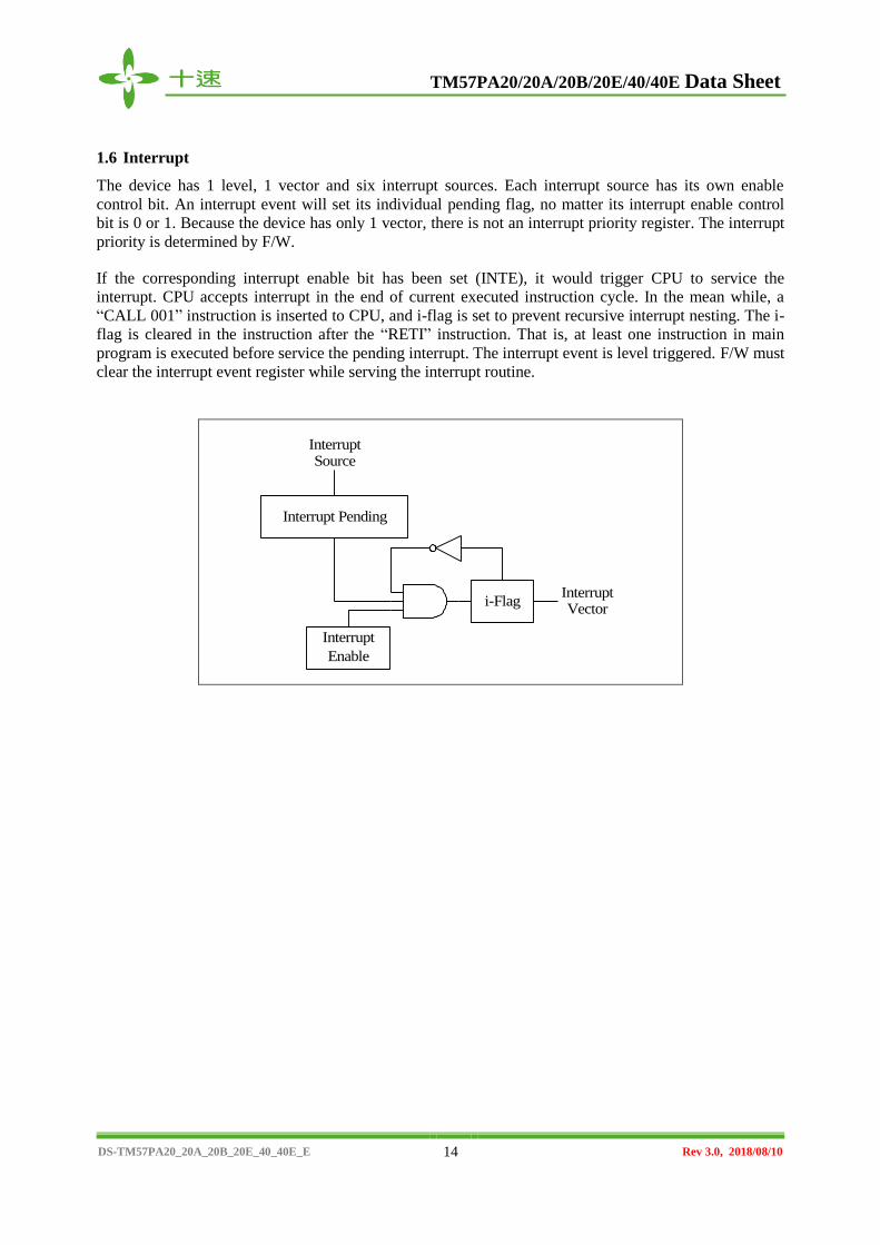
1.6 Interrupt
The device has 1 level, 1 vector and six interrupt sources. Each interrupt source has its own enable
control bit. An interrupt event will set its individual pending flag, no matter its interrupt enable control
bit is 0 or 1. Because the device has only 1 vector, there is not an interrupt priority register. The interrupt
priority is determined by F/W.
If the corresponding interrupt enable bit has been set (INTE), it would trigger CPU to service the
interrupt. CPU accepts interrupt in the end of current executed instruction cycle. In the mean while, a
“CALL 001” instruction is inserted to CPU, and i-flag is set to prevent recursive interrupt nesting. The i-
flag is cleared in the instruction after the “RETI” instruction. That is, at least one instruction in main
program is executed before service the pending interrupt. The interrupt event is level triggered. F/W must
clear the interrupt event register while serving the interrupt routine.
Interrupt Pending
Interrupt Vector
i-Flag
Interrupt Source
Interrupt
Enable
TM57PA20/20A/20B/20E/40/40E Data Sheet
DS-TM57PA20_20A_20B_20E_40_40E_E 15 Rev 3.0, 2018/08/10
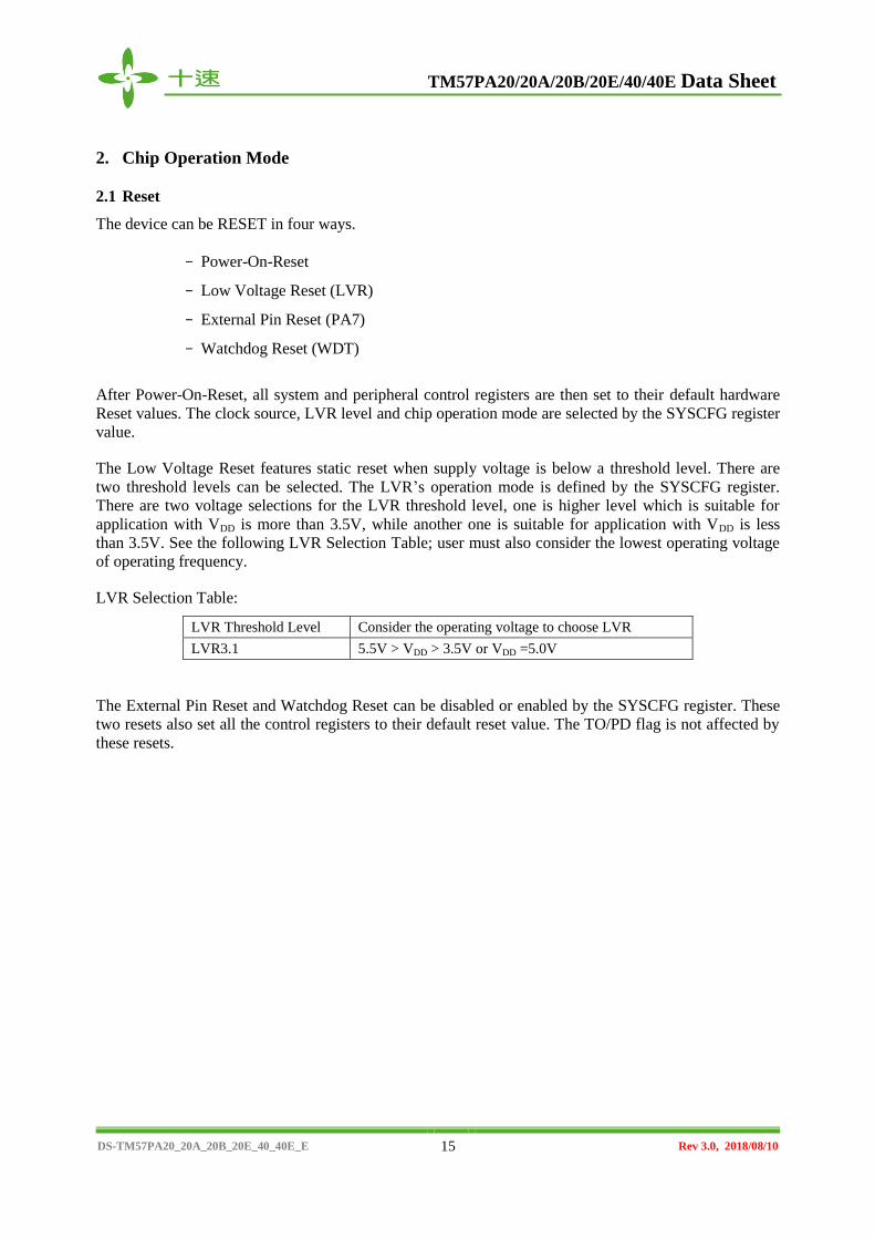
2. Chip Operation Mode
2.1 Reset
The device can be RESET in four ways.
- Power-On-Reset
- Low Voltage Reset (LVR)
- External Pin Reset (PA7)
- Watchdog Reset (WDT)
After Power-On-Reset, all system and peripheral control registers are then set to their default hardware
Reset values. The clock source, LVR level and chip operation mode are selected by the SYSCFG register
value.
The Low Voltage Reset features static reset when supply voltage is below a threshold level. There are
two threshold levels can be selected. The LVR’s operation mode is defined by the SYSCFG register.
There are two voltage selections for the LVR threshold level, one is higher level which is suitable for
application with VDD is more than 3.5V, while another one is suitable for application with VDD is less
than 3.5V. See the following LVR Selection Table; user must also consider the lowest operating voltage
of operating frequency.
LVR Selection Table:
LVR Threshold Level Consider the operating voltage to choose LVR
LVR3.1 5.5V > VDD > 3.5V or VDD =5.0V
The External Pin Reset and Watchdog Reset can be disabled or enabled by the SYSCFG register. These
two resets also set all the control registers to their default reset value. The TO/PD flag is not affected by
these resets.

TM57PA20/20A/20B/20E/40/40E Data Sheet
DS-TM57PA20_20A_20B_20E_40_40E_E 16 Rev 3.0, 2018/08/10
2.2 System Configuration Register (SYSCFG)
The System Configuration Register (SYSCFG) is located at ROM address FFCh. The SYSCFG
determines the option for initial condition of MCU. It is written by PROM Writer only. User can select
clock source, LVR threshold voltage and chip operation mode by SYSCFG register. The 13th bit of
SYSCFG is code protection selection bit. If this bit is 0, the data in PROM will be protected, when user
reads PROM.
Bit 13~0
Default Value 11_1111_111x_xxxx
Bit Description
13
PROTECT: Code Protection Selection
1 No protect
0 Code protection
12
nREUSE: PROM Re-use Control
1 Not Re-use
0 Re-use (TM57PA20/20A/20B do not support)
11-10
LVR: LV reset mode
11 Reserved
01 3.1V, always enable
10 Reserved
00 Disable (TM57PA20A only)
9-8
CLKT: Clock Source Selection
11 Fast Xtal (455 KHz~24 MHz)
10 Slow Xtal (32 KHz)
01 Internal RC FIRC4MHz; 8MHz (PA20A/PA20B only)
00 External RC
7
XRSTE: External pin(PA7) Reset Enable
1 Enable External pin Reset
0 Disable External pin Reset
6
WDTE: WDT Reset Enable
1 Enable WDT Reset, Disable WKT Timer
0 Disable WDT Reset, Enable WKT Timer
5-0 Reserved

TM57PA20/20A/20B/20E/40/40E Data Sheet
DS-TM57PA20_20A_20B_20E_40_40E_E 17 Rev 3.0, 2018/08/10
2.3 PROM Re-use
The PROM size of TM57PA40 is 4K words. For some F/W program, the program size could be less than
2K words. To fully utilize the PROM, the device allows users to reuse the PROM. This feature is named
as Two Time Programmable (TTP) ROM. While the first half of PROM is occupied by a useless
program code and the second half of the PROM remains blank, users can re-write the PROM with the
updated program code into the second half of the PROM. In the Re-use mode, the Reset Vector and
Interrupt Vector are re-allocated at the beginning of the PROM's second half by the Assembly Compiler.
Users simply choose the "REUSE" option in the ICE tool interface, and then the Compiler will move the
object code to proper location. That is, the user's program still has reset vector at address 000h, but the
compiled object code has reset vector at 800h. In the SYSCFG, if nPROTECT=0 and nREUSE=1, the
Code protection area is first half of PROM. This allows the Writer tool to write then verify the Code
during the Re-use Code programming. After the Re-use Code being written into the PROM's second half,
user should write "nREUSE" control bit to "0". In the mean while, the Code protection area becomes the
whole PROM except the Reserved Area.
PROM, nREUSE=1 PROM, nREUSE=0
000 Reset Vector 000 001 Interrupt Vector 001
Code Useless Protect Code
Area
User Code
7FF Code 7FF Protect
800 800 Reset Vector Area 801 801 Interrupt Vector
User
Code
FFC SYSCFG FFC SYSCFG FFD Manufacturer FFD Manufacturer FFE Reserved FFE Reserved
FFF Area FFF Area
For TM57PA20/20E, user code usable range is 0x000~0x7FF. For TM57PA20A/20B, user code usable
range is 0x000~0x7FB. TM57PA20/20A/20B don’t support REUSE function any more. The HEX file of
TM57PA20 can convert to TM57PA20A/20B/20E HEX via TICE99 IDE tools.
1.4 Power-Down Mode
The Power-down mode is activated by SLEEP instruction. During the Power-down mode, the system
clock and peripherals stop to minimize power consumption, while the WDT/WKT Timer is working or
not depends on F/W setting. The Power down mode can be terminated by Reset, or enabled Interrupts
(External pins and WKT interrupt).

TM57PA20/20A/20B/20E/40/40E Data Sheet
DS-TM57PA20_20A_20B_20E_40_40E_E 18 Rev 3.0, 2018/08/10
3. Peripheral Functional Block
1.1 Watchdog (WDT) / Wakeup (WKT) Timer
The WDT and WKT share the same internal RC Timer. The overflow period of WDT/WKT can be
selected from 13 ms to 140 ms. The WDT/WKT is cleared by the CLRWDT instruction. If the Watchdog
Reset is enabled (WDTE=1), the WDT generates the chip reset signal, even in sleep mode, otherwise, the
WKT only generates overflow time out interrupt. If WDTE=0 and WKTIE=0 (Wakeup interrupt disable),
the internal RC Timer stops for power saving.
nRESET
XRESETE
Power On Reset
Low Voltage Detector
WDTE
4
WKTIE
EN
WatchdogRC-OSC
WDTE
CLR
WDT/WKT Timer WKTIE
“CLRWDT”
Wake Up Timer Interrupt
Time Out
System Reset
WKTPSC[1:0]
“SLEEP”
SLEEP_ MODE
2LVR[1:0]
System Clock
VDD
VDD
EN
Oscillator
SLEEP_ MODE
VDD
2
SLEEP_ MODE
D Q
RN
TM57PA20/20A/20B/20E/40/40E Data Sheet
DS-TM57PA20_20A_20B_20E_40_40E_E 19 Rev 3.0, 2018/08/10
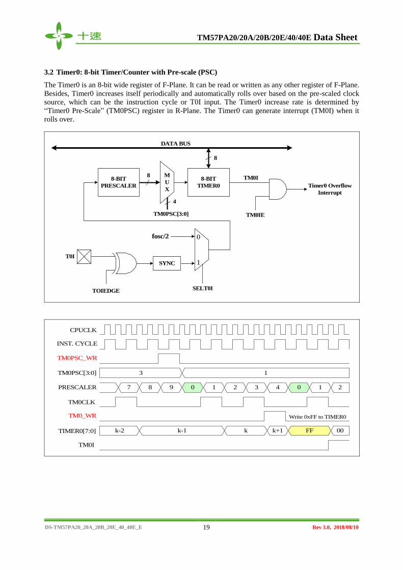
3.2 Timer0: 8-bit Timer/Counter with Pre-scale (PSC)
The Timer0 is an 8-bit wide register of F-Plane. It can be read or written as any other register of F-Plane.
Besides, Timer0 increases itself periodically and automatically rolls over based on the pre-scaled clock
source, which can be the instruction cycle or T0I input. The Timer0 increase rate is determined by
“Timer0 Pre-Scale” (TM0PSC) register in R-Plane. The Timer0 can generate interrupt (TM0I) when it
rolls over.
8-BIT
TIMER0
8-BIT
PRESCALER
SYNC
TOIEDGE
1
0fosc/2
T0I
TM0IE
Timer0 Overflow
Interrupt
TM0I
DATA BUS
SELT0I
M
U
X
TM0PSC[3:0]
4
8
8
7 8 9 0 1 2 3 4 0 1
CPUCLK
INST. CYCLE
TM0PSC_WR
TM0_WR
PRESCALER
TM0CLK
3TM0PSC[3:0]
TIMER0[7:0]
TM0I
k k+1 FF
2
00k-1k-2
1
Write 0xFF to TIMER0

TM57PA20/20A/20B/20E/40/40E Data Sheet
DS-TM57PA20_20A_20B_20E_40_40E_E 20 Rev 3.0, 2018/08/10
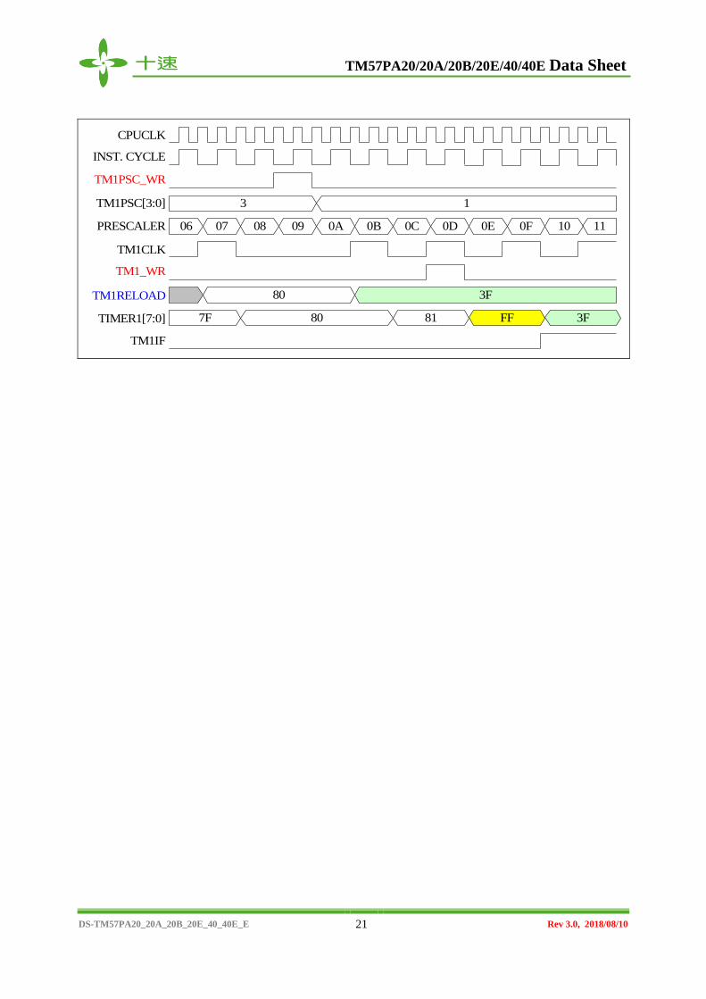
3.3 Timer1: 8-bit Timer with Pre-scale (PSC)
The Timer1 is an 8-bit wide register of F-Plane. It can be read or written as any other register of F-Plane.
Besides, Timer1 increases itself periodically and automatically reloads a new “offset value” (TM1RELD)
while it rolls over based on the pre-scaled instruction clock. The Timer1 increase rate is determined by
“Timer1 Pre-Scale” (TM1PSC) register in R-Plane. The Timer1 can generate interrupt (TM1I) and
T1OUT toggle signal when it rolls over.
8-BIT
TIMER1
8-BIT
PRESCALERfosc/2
TM1IE
Timer1 Overflow
Interrupt
TM1I
DATA BUS
M
U
X
TM1PSC[3:0]
TM1RELD
8
8
88
4
FF
TIMER1[7:0]
TM1I
Soltware
Clear
K
K
TM1RELD[7:0]
T1OUT
TM57PA20/20A/20B/20E/40/40E Data Sheet
DS-TM57PA20_20A_20B_20E_40_40E_E 21 Rev 3.0, 2018/08/10
CPUCLK
INST. CYCLE
07 08 09 0A 0B 0C 0D 0E 0F 10
TM1PSC_WR
TM1_WR
PRESCALER
TM1CLK
3TM1PSC[3:0]
TIMER1[7:0]
TM1IF
81 FF
11
807F
1
06
80 3FTM1RELOAD
3F

TM57PA20/20A/20B/20E/40/40E Data Sheet
DS-TM57PA20_20A_20B_20E_40_40E_E 22 Rev 3.0, 2018/08/10
3.4 8+2 bit PWM
PWM0 and PWM1 have the same structure. The PWM can generate fix frequency waveform with 1024
duty resolution based on System Clock. A spread LSB technique allows PWM to run its frequency at
“System Clock divided by 256” instead of “System Clock divided by 1024”, which means the PWM is 4
times faster than normal. The advantage of higher PWM frequency is that the post RC filter can
transform the PWM signal to more stable DC voltage level. The PWM output signal reset to low level
whenever the 8-bit base counter matches the 8-bit MSB of PWM duty register (PWMDUTY). When the
base counter rolls over, the 2-bit LSB of PWM duty register decide whether to set the PWM output
signal high immediately or set it high after one clock cycle delay.
PWMDUTY
8-bit MSB
8-BIT BASE
COUNTER
PWMDUTY
2-bit LSB
DUTY
EXTENSION
LOGIC
R
S
QOVERFLOW
RESETnSystem Clock
2
8
EQ
8
PWM Output

TM57PA20/20A/20B/20E/40/40E Data Sheet
DS-TM57PA20_20A_20B_20E_40_40E_E 23 Rev 3.0, 2018/08/10
Frame #0 Frame #1 Frame #2 Frame #3
256 clock
PWMDUTY[1:0] = 0
PWMDUTY[9:2] = 0
PWMDUTY[1:0] = 1
PWMDUTY[9:2] = 0
PWMDUTY[1:0] = 2
PWMDUTY[9:2] = 0
PWMDUTY[1:0] = 3
PWMDUTY[9:2] = 0
PWMDUTY[1:0] = 0
PWMDUTY[9:2] = t
PWMDUTY[1:0] = 1
PWMDUTY[9:2] = t
PWMDUTY[1:0] = 2
PWMDUTY[9:2] = t
PWMDUTY[1:0] = 3
PWMDUTY[9:2] = t
t clock
1 clock
256 clock 256 clock 256 clock
BASE
COUNTER[7:0]
PWM example code:
movlw 01111111b
movwf 0ch ;set PWM0DUTY[9:2]=8’b01111111
movlw 11000000b
movwf 0dh ;set PWM0DUTY[1:0]=2’b11
movlw 01000000b
movwr 0bh ;enable PWM0 output to PA0 (PWM0_OUT)
:
:
movlw 00h
movwr 0bh ;disable PWM0 (PWM0_OUT)

TM57PA20/20A/20B/20E/40/40E Data Sheet
DS-TM57PA20_20A_20B_20E_40_40E_E 24 Rev 3.0, 2018/08/10
3.5 12-bit ADC
Analog
Switch
AD0
AD1
3
ADCSEL[2:0]
ADCSTART
Successive
Approximation
ADC
12
Timing Control
ADC
Clock
Prescalerfosc/2
M
U
X
ADCLK
3
ADCLKS[2:0]End of Conversion
( EOC )
Sample/Hold
8
AD6
AD7
ADCDATA:
:
The 12-bit ADC (Analog to Digital Converter) consists of an 8-channel analog input multiplexer, control
register, clock generator, 12-bit successive approximation register, and output data register. To use the
ADC, user needs to set ADCLKS to choose a proper ADC clock frequency, which must be less than 2
MHz. User then launches the ADC conversion by setting the ADCSTART control bit. After end of
conversion, H/W automatically clears the ADCSTAT bit. User can poll this bit to know the conversion
status. The nADC_IE control register is used for ADC pin type setting, user can write the corresponding
bit to “0” when the pin is used as an ADC input. The setting can disable the pin logical input path to save
power consumption.
ADCSTART
End of Conversion
bit11 bit10 bit9 … bit3 bit2 bit2 bit1 bit0 ADCDATA(n)000ADCDATA(n-1)ADCDATA[11:0]
Signal Sample and Hold
50 ADC Clock Cycles
Conversion Time
24 ADC Clock Cycles

TM57PA20/20A/20B/20E/40/40E Data Sheet
DS-TM57PA20_20A_20B_20E_40_40E_E 25 Rev 3.0, 2018/08/10
ADC example code:
movlw 00000111b
movwf 11h ;ADC channel select,ADC7(PB0) (ADCSEL)
movlw 00000001h
movwr 09h ;disable PB0 pull up resistor (nPBPU)
movlw 01111111b
movwr 12h ;set ADC7 input enable (nADC_IE)
movlw 00010000b
movwr 0ch ;set ADC clock is instruction cycle / 64 (ADCCLKS)
bsf 11h,3 ;start ADC conversion (ADCSTART)
ADC_LOOP:
btfsc 11h,3
goto ADC_LOOP ;wait ADCSTART go LOW
: ;read ADCQ[11:0] (ADCDQ)
:

TM57PA20/20A/20B/20E/40/40E Data Sheet
DS-TM57PA20_20A_20B_20E_40_40E_E 26 Rev 3.0, 2018/08/10
3.6 System Clock Oscillator
System Clock can be operated in four different oscillation modes, which is selected by setting the CLKS
in the SYSCFG register. In Slow/Fast Crystal mode, a crystal or ceramic resonator is connected to the
Xin and Xout pins to establish oscillation. In external RC mode, the external resistor and capacitor
determine the oscillation frequency. In the internal RC mode, the on chip oscillator generates 4 MHz
system clock. In this mode, PCB Layout may have strong effect on the stability of Internal Clock
Oscillator. Since power noise degrades the performance of Internal Clock Oscillator, placing power
supply bypass capacitors 1 uF and 0.1 uF very close to VDD/VSS pins improves the stability of clock and
the overall system.
XIN
XOUT
C1
C2
Xrc
External Oscillator Circuit
(Crystal or Ceramic)
External RC Oscillator
Vss
Vdd
1uF0.1uF
Internal RC Mode
TM57PA20/20A/20B/20E/40/40E Data Sheet
DS-TM57PA20_20A_20B_20E_40_40E_E 27 Rev 3.0, 2018/08/10
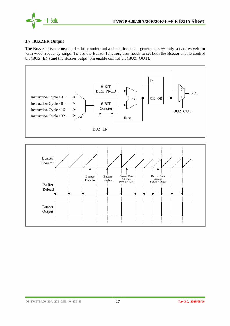
3.7 BUZZER Output
The Buzzer driver consists of 6-bit counter and a clock divider. It generates 50% duty square waveform
with wide frequency range. To use the Buzzer function, user needs to set both the Buzzer enable control
bit (BUZ_EN) and the Buzzer output pin enable control bit (BUZ_OUT).
EQ
6-BIT
BUZ_PROD
6-BIT
Conuter
Instruction Cycle / 4
Instruction Cycle / 8
Instruction Cycle / 16
Instruction Cycle / 32
BUZ_EN
D
CK QB
Reset
PD1
BUZ_OUT
0
1
Buzzer
Counter
Buffer
Reload
Buzzer
Output
Buzzer DataChange
Before > After
Buzzer DataChange
Before < After
Buzzer
Disable
Buzzer
Enable
TM57PA20/20A/20B/20E/40/40E Data Sheet
DS-TM57PA20_20A_20B_20E_40_40E_E 28 Rev 3.0, 2018/08/10
BUZ_PROD[5:0] determines output frequency. Frequency calculation is as follows.
FBZ = (fOSC/2) / (Instruction Cycle Divider) / (BUZ_PROD +1) / 2
Output frequency calculation
CPU Clock (fosc) = 8192 KHz Instruction Cycle = fosc/2 = 8192 KHz/2 = 4096 KHz Prescaler Ratio (BUZ_PSC) = 2’b11 (Instruction Cycle Divider = 32) Period Data (BUZ_PROD) = 9 FBZ = (8192 KHz/2) / 32 / (9+1) / 2 = 6.4 (KHz)
BUZZER example code:
movlw 10000000b movwr 0bh ; enable BUZZER output to PD1 (BUZ_OUT) movlw 11001001b ; (fosc/2)/32 (BUZ_PSC) movwr 10h ; Period=9 (BUZ_PROD) movlw 80h movwr 0ch ; enable BUZZER counting (BUZ_EN) : : movlw 00h movwr 0ch ; disable BUZZER counting (BUZ_EN)

TM57PA20/20A/20B/20E/40/40E Data Sheet
DS-TM57PA20_20A_20B_20E_40_40E_E 29 Rev 3.0, 2018/08/10
4. I/O Port
4.1 PA0-2
These pins can be used as Schmitt-trigger input, CMOS push-pull output or “pseudo-open-drain” output.
The pull-up resistor is assignable to each pin by S/W setting. To use the pin in Schmitt-trigger input
mode, S/W needs to set the PAE=0 and PAD=1. To use the pin in pseudo-open-drain mode, S/W sets
the PAE=0. The benefit of pseudo-open-drain structure is that the output rise time can be much faster
than pure open-drain structure. S/W sets PAE=1 to use the pin in CMOS push-pull output mode. Reading
the pin data (PAD) has different meaning. In “Read-Modify-Write” instruction, CPU actually reads the
output data register. In the other instructions, CPU reads the pin state. The so-called “Read-Modify-Write”
instruction includes BSF, BCF and all instructions using F-Plane as destination.
D Q
D Q
D Q
WR_PAD
WR_PAE
DATA
Write
Pin
PAE
SN
RN
SYS_RESETn
RNWR_nPAPU
nPAPU
1
0
RD_PADRead_Modify_Write
Rpull-up
PADPort
Pre-Driver
MP
MR
MN
Delay
1 CLK
DATA Read
MN
Drive
PAE
PAD
MP
Drive
1 CLK
PA0-2, nPAPU=0
MN
Drive
MN
Drive
MR
Drive
MP
Drive

TM57PA20/20A/20B/20E/40/40E Data Sheet
DS-TM57PA20_20A_20B_20E_40_40E_E 30 Rev 3.0, 2018/08/10
4.2 PA3-6, PB0-1, PD0-7
These pins are almost the same as PA0-2, except they do not support pseudo-open-drain mode. They can
be used in pure open-drain mode, instead.
D Q
D Q
D Q
WR_PAD
WR_PAE
DATA Write
Pin
PAE
SN
RN
SYS_RESETn
RNWR_nPAPU
nPAPU
1
0
RD_PADRead_Modify_Write
Rpull-up
PAD Port
Pre-Driver
MP
MR
MN
DATA Read
MN
Drive
PAE
PAD
PA3-6, nPAPU=0
MN
Drive
MN
Drive
MR
Drive
MP
Drive

TM57PA20/20A/20B/20E/40/40E Data Sheet
DS-TM57PA20_20A_20B_20E_40_40E_E 31 Rev 3.0, 2018/08/10
4.3 PA7
PA7 can be only used in Schmitt-trigger input mode. The pull-up resistor is always connected to this pin.
D Q
WR_PAD
DATA Write
PinSN
SYS_RESETn
1
0
RD_PADRead_Modify_Write
Rpull-upPAD
DATA Read

TM57PA20/20A/20B/20E/40/40E Data Sheet
DS-TM57PA20_20A_20B_20E_40_40E_E 32 Rev 3.0, 2018/08/10
MEMORY MAP
F-Plane
Name Address R/W Rst Description
INDF 00.7~0 R/W - Not a physical register, addressing INDF actually point to the register
whose address is contained in the FSR register
TIMER0 01.7~0 R/W 0 Timer0 content
PC 02.7~0 R/W 0 Programming Counter [7~0]
RAMBANK 03.5 R/W 0 RAM Bank Selection
TO 03.4 R 0 WDT time out flag, cleared by ‘SLEEP’, ‘CLRWDT’ instruction
PD 03.3 R 0 Sleep mode flag, cleared by ‘CLRWDT’ instruction
ZFLAG 03.2 R/W 0 Zero Flag
DCFLAG 03.1 R/W 0 Decimal Carry Flag
CFLAG 03.0 R/W 0 Carry Flag
FSR 04.7 R 0 Fixed 0
04.6~0 R/W - File Select Register, indirect address mode pointer
PA[7] 05.7 R - PA7 pin state
PAD[6:0] 05.6~0 R - Port A pin or “data register” state
W 7F Port A output data register
PBD[1:0] 06.1~0 R - Port B pin or “data register” state
W 3 Port B output data register
PDD[7:0] 07.7~0 R - Port D pin or “data register” state
W FF Port D output data register
TM1I 09.5 R -
Timer1 interrupt event pending flag, set by H/W while Timer1
overflows
W 0 write 0: clear this flag; write 1: no action
TM0I 09.4 R -
Timer0 interrupt event pending flag, set by H/W while Timer0
overflows
W 0 write 0: clear this flag; write 1: no action
WKTI 09.3 R - WKT interrupt event pending flag, set by H/W while WKT time out
W 0 write 0: clear this flag; write 1: no action
XINT2 09.2 R -
INT2 pin (PA7) interrupt event pending flag, set by H/W at INT2
pin’s falling edge
W 0 write 0: clear this flag; write 1: no action

TM57PA20/20A/20B/20E/40/40E Data Sheet
DS-TM57PA20_20A_20B_20E_40_40E_E 33 Rev 3.0, 2018/08/10
Name Address R/W Rst Description
XINT1 09.1 R -
INT1 pin (PA1) interrupt event pending flag, set by H/W at INT1
pin’s falling or rising edge
W 0 write 0: clear this flag; write 1: no action
XINT0 09.0 R -
INT0 pin (PA6) interrupt event pending flag, set by H/W at INT0
pin’s falling edge
W 0 write 0: clear this flag; write 1: no action
TIMER1 0a.7~0 R/W 0 Timer1 content
PWM0DUTY 0c.7~0 R/W 0 PWM0 duty 8-bit MSB
0d.7~6 R/W 0 PWM0 duty 2-bit LSB
PWM1DUTY 0e.7~0 R/W 0 PWM1 duty 8-bit MSB
0f.7~6 R/W 0 PWM1 duty 2-bit LSB
ADCDQ 10.7~0 R - ADC conversion result ADCQ[11:4]
11.7~4 R - ADC conversion result ADCQ[3:0]
ADCSTART 11.3 R - H/W clears this bit after ADC end of conversion
W 0 S/W sets this bit to start ADC conversion
ADCSEL 11.2~0 R/W 0 ADC channel select; 0: ADC0, 1: ADC1,…,7: ADC7
RAM 20~27 R/W - Internal RAM – Common Area
28~7F R/W - Internal RAM – RAM Bank0
28~7F R/W - Internal RAM – RAM Bank1

TM57PA20/20A/20B/20E/40/40E Data Sheet
DS-TM57PA20_20A_20B_20E_40_40E_E 34 Rev 3.0, 2018/08/10
R-Plane
Name Address R/W Rst Description
TCOUT_PSC 02.7~6 W 0
TCOUT Pre-Scale
00: TCOUT output clock is “Instruction Cycle” divided by 1
01: TCOUT output clock is “Instruction Cycle” divided by 2
10: TCOUT output clock is “Instruction Cycle” divided by 4
11: TCOUT output clock is “Instruction Cycle” divided by 8
T0IEDGE 02.5 W 0 0: T0I(PA2) rising edge to increase Timer0/PSC count
1: T0I(PA2) falling edge to increase Timer0/PSC count
SELT0I 02.4 W 0 0: Timer0/PSC clock source is “Instruction Cycle”
1: Timer0/PSC clock source is T0I pin
TM0PSC 02.3~0 W 0
Timer0 Pre-Scale
0000: Timer0 input clock is “Instruction Cycle” divided by 1
0001: Timer0 input clock is “Instruction Cycle” divided by 2
~
0111: Timer0 input clock is “Instruction Cycle” divided by 128
1000: Timer0 input clock is “Instruction Cycle” divided by 256
PWRDOWN 03 W write this register to enter Power-Down Mode
CLRWDT 04 W write this register to clear WDT/WKT
PAE
05.6~3 W 0
Each bit controls its corresponding pin, if the bit is
0: the pin is open-drain output or Schmitt-trigger input
1: the pin is CMOS push-pull output
05.2~0 W 0
Each bit controls its corresponding pin, if the bit is
0: the pin is pseudo-open-drain output or Schmitt-trigger input
1: the pin is CMOS push-pull output
PBE 06.1~0 W 0
Each bit controls its corresponding pin, if the bit is
0: the pin is open-drain output or Schmitt-trigger input
1: the pin is CMOS push-pull output
PDE 07.7~0 W 0
Each bit controls its corresponding pin, if the bit is
0: the pin is open-drain output or Schmitt-trigger input
1: the pin is CMOS push-pull output
nPAPU 08.6~0 W 0
Each bit controls its corresponding pin, if the bit is
0: the pin pull up resistor is enabled, except
a. the pin’s output data register (PAD) is 0
b. the pin’s CMOS push-pull mode is chosen (PAE=1)
c. the pin is working for Crystal or external RC oscillation
d. PA0 is working for PWM0 output
1: the pin pull up resistor is disabled
nPBPU 09.1~0 W 0
Each bit controls its corresponding pin, if the bit is
0: the pin pull up resistor is enabled, except
a. the pin’s output data register (PBD) is 0
b. the pin’s CMOS push-pull mode is chosen (PBE=1)
c. PB0 is working for PWM1 output
1: the pin pull up resistor is disabled
nPDPU 0a.7~0 W 0
Each bit controls its corresponding pin, if the bit is
0: the pin pull up resistor is enabled, except
a. the pin’s output data register (PDD) is 0
b. the pin’s CMOS push-pull mode is chosen (PDE=1)
c. the pin is working for T1OUT/BUZZER/TCOUT output
1: the pin pull up resistor is disabled
BUZ_OUT 0b.7 W 0 0: disable BUZZER output to PD1 pin
1: enable BUZZER output to PD1 pin

TM57PA20/20A/20B/20E/40/40E Data Sheet
DS-TM57PA20_20A_20B_20E_40_40E_E 35 Rev 3.0, 2018/08/10
Name Address R/W Rst Description
PWM0_OUT 0b.6 W 0 0: disable PWM0 output to PA0 pin
1: enable PWM0 output to PA0 pin
PWM1_OUT 0b.5 W 0 0: disable PWM1 output to PB0 pin
1: enable PWM1 output to PB0 pin
INT1EDGE 0b.4 W 0 0: INT1 pin (PA1) falling edge to trigger interrupt event
1: INT1 pin (PA1) rising edge to trigger interrupt event
TC_OUT 0b.3 W 0 0: disable Instruction Clock divider output to PD6 pin
1: enable Instruction Clock divider output to PD6 pin
TM1_OUT 0b.2 W 0 0: disable Timer1 match out (T1OUT) to PD0
1: enable Timer1 match out (T1OUT) to PD0
WKTPSC 0b.1~0 W 11
WDT/WKT period (VDD=5V)
00: 13 ms
01: 25 ms
10: 50 ms
11: 100 ms
BUZ_EN 0c.7 W 0 0: disable BUZZER timer counting
1: enable BUZZER timer counting
ADCLKS 0c.6~4 W 0
000: ADC clock is “Instruction Cycle” divided by 128
001: ADC clock is “Instruction Cycle” divided by 64
~
111: ADC clock is “Instruction Cycle” divided by 1
TM1PSC 0c.3~0 W 0
0000: Timer1 input clock is “Instruction Cycle” divided by 1
0001: Timer1 input clock is “Instruction Cycle” divided by 2
~
0111: Timer1 input clock is “Instruction Cycle” divided by 128
1000: Timer1 input clock is “Instruction Cycle” divided by 256
TM1RELD 0d.7~0 W 0 Timer1 reload offset value while it rolls over
TM1IE 0e.5 W 0 Timer1 interrupt enable, 1=enable, 0=disable
TM0IE 0e.4 W 0 Timer0 interrupt enable, 1=enable, 0=disable
WKTIE 0e.3 W 0 Wakeup Timer interrupt enable, 1=enable, 0=disable
XINT2E 0e.2 W 0 INT2 pin (PA7) interrupt enable, 1=enable, 0=disable
XINT1E 0e.1 W 0 INT1 pin (PA1) interrupt enable, 1=enable, 0=disable
XINT0E 0e.0 W 0 INT0 pin (PA6) interrupt enable, 1=enable, 0=disable
TESTREG 0f.1~0 W 0 Test mode register, for manufacturer only, user does not write it
BUZ_PSC 10.7~6 W 0
BUZZER Clock Prescaler
00: BUZZER clock is “Instruction Cycle” divided by 4
01: BUZZER clock is “Instruction Cycle” divided by 8
10: BUZZER clock is “Instruction Cycle” divided by 16
11: BUZZER clock is “Instruction Cycle” divided by 32
BUZ_PROD 10.5~0 W 0 BUZZER Period Data. BUZZER output is BUZZER Clock divided by
BUZ_PROD
ADC_TRIM 11.2~0 W 0 Test mode register, for manufacturer only, user does not write it
nADC_IE 12.7~0 W ff
Each bit controls its corresponding ADC7~0 enable pin, if the bit is
0: the corresponding pin is ADC input
1: the corresponding pin is digital input
TM57PA20/20A/20B/20E/40/40E Data Sheet
DS-TM57PA20_20A_20B_20E_40_40E_E 36 Rev 3.0, 2018/08/10
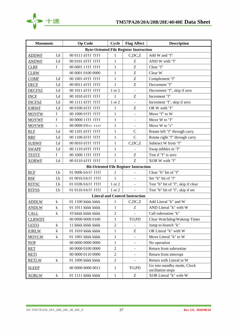
INSTRUCTION SET
Each instruction is a 14-bit word divided into an OPCODE, which specifies the instruction type, and one
or more operands, which further specify the operation of the instruction. The instructions can be
categorized as byte-oriented, bit-oriented and literal operations list in the following table.
For byte-oriented instructions, “f” or “r” represents the address designator and “d” represents the
destination designator. The address designator is used to specify which address in Program memory is to
be used by the instruction. The destination designator specifies where the result of the operation is to be
placed. If “d” is “0”, the result is placed in the W register. If “d” is “1”, the result is placed in the address
specified in the instruction.
For bit-oriented instructions, “b” represents a bit field designator, which selects the number of the bit
affected by the operation, while “f” represents the address designator. For literal operations, “k”
represents the literal or constant value.
Field / Legend Description
f F-Plane Register File Address
r R-Plane Register File Address
b Bit address
k Literal. Constant data or label
d Destination selection field, 0: Working register, 1: Register file
W Working Register
Z Zero Flag
C Carry Flag
DC Decimal Carry Flag
PC Program Counter
TOS Top Of Stack
GIE Global Interrupt Enable Flag (i-Flag)
[] Option Field
( ) Contents
. Bit Field
B Before
A After
← Assign direction
TM57PA20/20A/20B/20E/40/40E Data Sheet
DS-TM57PA20_20A_20B_20E_40_40E_E 37 Rev 3.0, 2018/08/10
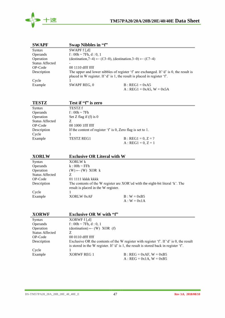
Mnemonic Op Code Cycle Flag Affect Description
Byte-Oriented File Register Instruction
ADDWF f,d 00 0111 d f f f f f f f 1 C,DC,Z Add W and "f"
ANDWF f,d 00 0101 d f f f f f f f 1 Z AND W with "f"
CLRF f 00 0001 1 f f f f f f f 1 Z Clear "f"
CLRW 00 0001 0100 0000 1 Z Clear W
COMF f,d 00 1001 d f f f f f f f 1 Z Complement "f"
DECF f,d 00 0011 d f f f f f f f 1 Z Decrement "f"
DECFSZ f,d 00 1011 d f f f f f f f 1 or 2 - Decrement "f", skip if zero
INCF f,d 00 1010 d f f f f f f f 1 Z Increment "f"
INCFSZ f,d 00 1111 d f f f f f f f 1 or 2 - Increment "f", skip if zero
IORWF f,d 00 0100 d f f f f f f f 1 Z OR W with "f"
MOVFW f 00 1000 0 f f f f f f f 1 - Move "f" to W
MOVWF f 00 0000 1 f f f f f f f 1 - Move W to "f"
MOVWR r 00 0000 0 0 r r r r r r 1 - Move W to "r"
RLF f,d 00 1101 d f f f f f f f 1 C Rotate left "f" through carry
RRF f,d 00 1100 d f f f f f f f 1 C Rotate right "f" through carry
SUBWF f,d 00 0010 d f f f f f f f 1 C,DC,Z Subtract W from "f"
SWAPF f,d 00 1110 d f f f f f f f 1 - Swap nibbles in "f"
TESTZ f 00 1000 1 f f f f f f f 1 Z Test if "f" is zero
XORWF f,d 00 0110 d f f f f f f f 1 Z XOR W with "f"
Bit-Oriented File Register Instruction
BCF f,b 01 000b b b f f f f f f 1 - Clear "b" bit of "f"
BSF f,b 01 001b b b f f f f f f 1 - Set "b" bit of "f"
BTFSC f,b 01 010b b b f f f f f f 1 or 2 - Test "b" bit of "f", skip if clear
BTFSS f,b 01 011b b b f f f f f f 1 or 2 - Test "b" bit of "f", skip if set
Literal and Control Instruction
ADDLW k 01 1100 kkkk kkkk 1 C,DC,Z Add Literal "k" and W
ANDLW k 01 1011 kkkk kkkk 1 Z AND Literal "k" with W
CALL k 10 kkkk kkkk kkkk 2 - Call subroutine "k"
CLRWDT 00 0000 0000 0100 1 TO,PD Clear Watchdog/Wakeup Timer
GOTO k 11 kkkk kkkk kkkk 2 - Jump to branch "k"
IORLW k 01 1010 kkkk kkkk 1 Z OR Literal "k" with W
MOVLW k 01 1001 kkkk kkkk 1 - Move Literal "k" to W
NOP 00 0000 0000 0000 1 - No operation
RET 00 0000 0100 0000 2 - Return from subroutine
RETI 00 0000 0110 0000 2 - Return from interrupt
RETLW k 01 1000 kkkk kkkk 2 - Return with Literal in W
SLEEP 00 0000 0000 0011 1 TO,PD Go into standby mode, Clock
oscillation stops
XORLW k 01 1111 kkkk kkkk 1 Z XOR Literal "k" with W
TM57PA20/20A/20B/20E/40/40E Data Sheet
DS-TM57PA20_20A_20B_20E_40_40E_E 38 Rev 3.0, 2018/08/10
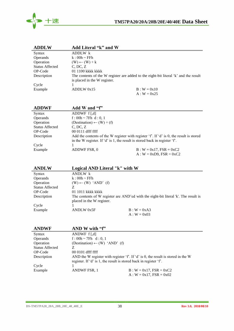
ADDLW Add Literal “k” and W Syntax ADDLW k
Operands k : 00h ~ FFh
Operation (W) ← (W) + k
Status Affected C, DC, Z
OP-Code 01 1100 kkkk kkkk
Description The contents of the W register are added to the eight-bit literal ‘k’ and the result
is placed in the W register.
Cycle 1
Example ADDLW 0x15 B : W = 0x10
A : W = 0x25
ADDWF Add W and “f” Syntax ADDWF f [,d]
Operands f : 00h ~ 7Fh d : 0, 1
Operation (Destination) ← (W) + (f)
Status Affected C, DC, Z
OP-Code 00 0111 dfff ffff
Description Add the contents of the W register with register ‘f’. If ‘d’ is 0, the result is stored
in the W register. If ‘d’ is 1, the result is stored back in register ‘f’.
Cycle 1
Example ADDWF FSR, 0 B : W = 0x17, FSR = 0xC2
A : W = 0xD9, FSR = 0xC2
ANDLW Logical AND Literal "k" with W Syntax ANDLW k
Operands k : 00h ~ FFh
Operation (W) ← (W) ‘AND’ (f)
Status Affected Z
OP-Code 01 1011 kkkk kkkk
Description The contents of W register are AND’ed with the eight-bit literal 'k'. The result is
placed in the W register.
Cycle 1
Example ANDLW 0x5F B : W = 0xA3
A : W = 0x03
ANDWF AND W with “f” Syntax ANDWF f [,d]
Operands f : 00h ~ 7Fh d : 0, 1
Operation (Destination) ← (W) ‘AND’ (f)
Status Affected Z
OP-Code 00 0101 dfff ffff
Description AND the W register with register ‘f’. If ‘d’ is 0, the result is stored in the W
register. If ‘d’ is 1, the result is stored back in register ‘f’.
Cycle 1
Example ANDWF FSR, 1 B : W = 0x17, FSR = 0xC2
A : W = 0x17, FSR = 0x02
TM57PA20/20A/20B/20E/40/40E Data Sheet
DS-TM57PA20_20A_20B_20E_40_40E_E 39 Rev 3.0, 2018/08/10
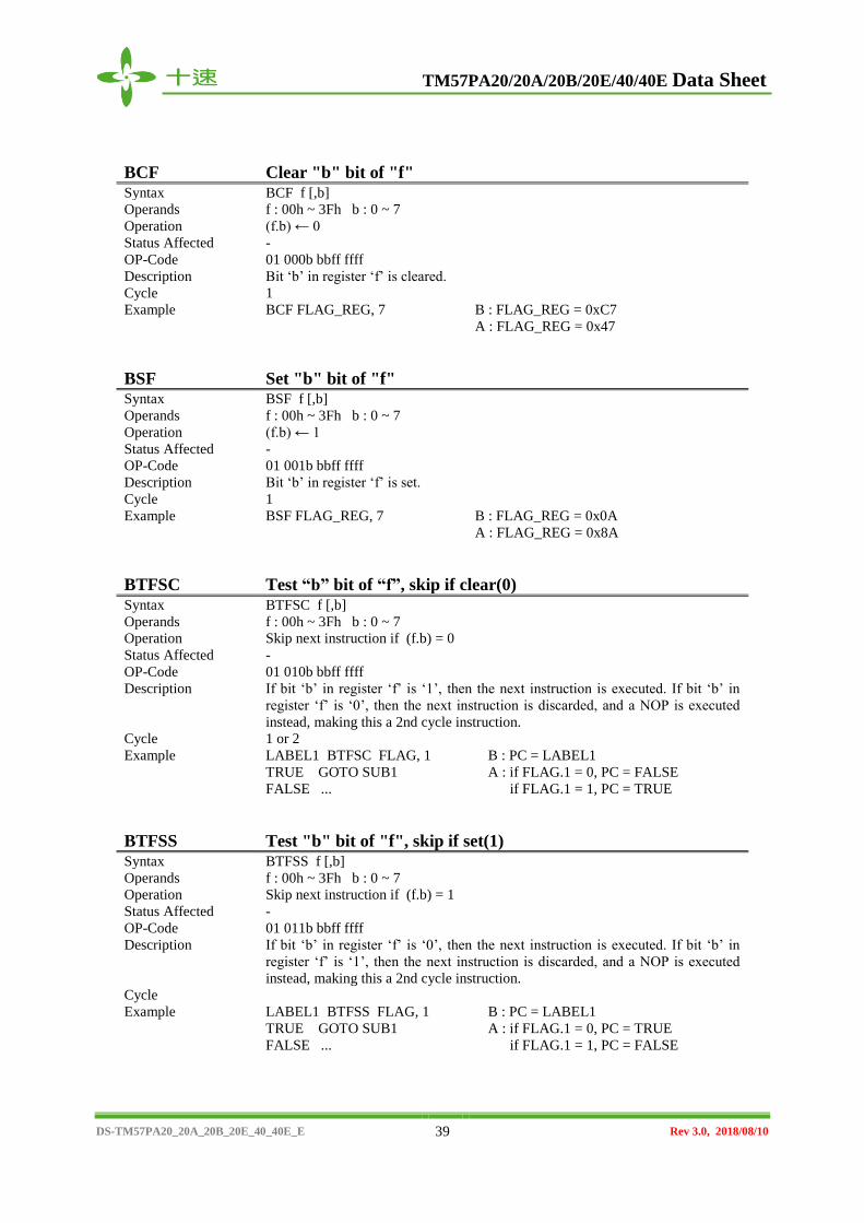
BCF Clear "b" bit of "f" Syntax BCF f [,b]
Operands f : 00h ~ 3Fh b : 0 ~ 7
Operation (f.b) ← 0
Status Affected -
OP-Code 01 000b bbff ffff
Description Bit ‘b’ in register ‘f’ is cleared.
Cycle 1
Example BCF FLAG_REG, 7 B : FLAG_REG = 0xC7
A : FLAG_REG = 0x47
BSF Set "b" bit of "f" Syntax BSF f [,b]
Operands f : 00h ~ 3Fh b : 0 ~ 7
Operation (f.b) ← 1
Status Affected -
OP-Code 01 001b bbff ffff
Description Bit ‘b’ in register ‘f’ is set.
Cycle 1
Example BSF FLAG_REG, 7 B : FLAG_REG = 0x0A
A : FLAG_REG = 0x8A
BTFSC Test “b” bit of “f”, skip if clear(0) Syntax BTFSC f [,b]
Operands f : 00h ~ 3Fh b : 0 ~ 7
Operation Skip next instruction if (f.b) = 0
Status Affected -
OP-Code 01 010b bbff ffff
Description If bit ‘b’ in register ‘f’ is ‘1’, then the next instruction is executed. If bit ‘b’ in
register ‘f’ is ‘0’, then the next instruction is discarded, and a NOP is executed
instead, making this a 2nd cycle instruction.
Cycle 1 or 2
Example LABEL1 BTFSC FLAG, 1
TRUE GOTO SUB1
FALSE ...
B : PC = LABEL1
A : if FLAG.1 = 0, PC = FALSE
if FLAG.1 = 1, PC = TRUE
BTFSS Test "b" bit of "f", skip if set(1) Syntax BTFSS f [,b]
Operands f : 00h ~ 3Fh b : 0 ~ 7
Operation Skip next instruction if (f.b) = 1
Status Affected -
OP-Code 01 011b bbff ffff
Description If bit ‘b’ in register ‘f’ is ‘0’, then the next instruction is executed. If bit ‘b’ in
register ‘f’ is ‘1’, then the next instruction is discarded, and a NOP is executed
instead, making this a 2nd cycle instruction.
Cycle
Example LABEL1 BTFSS FLAG, 1
TRUE GOTO SUB1
FALSE ...
B : PC = LABEL1
A : if FLAG.1 = 0, PC = TRUE
if FLAG.1 = 1, PC = FALSE

TM57PA20/20A/20B/20E/40/40E Data Sheet
DS-TM57PA20_20A_20B_20E_40_40E_E 40 Rev 3.0, 2018/08/10
CALL Call subroutine "k" Syntax CALL k
Operands K : 00h ~ FFFh
Operation Operation: TOS ← (PC)+ 1, PC.11~0 ← k
Status Affected -
OP-Code 10 kkkk kkkk kkkk
Description Call Subroutine. First, return address (PC+1) is pushed onto the stack. The 12-bit
immediate address is loaded into PC bits <11:0>. CALL is a two-cycle
instruction.
Cycle 2
Example LABEL1 CALL SUB1 B : PC = LABEL1
A : PC = SUB1, TOS = LABEL1+1
CLRF Clear “f” Syntax CLRF f
Operands f : 00h ~ 7Fh
Operation (f) ← 00h, Z ← 1
Status Affected Z
OP-Code 00 0001 1fff ffff
Description The contents of register ‘f’ are cleared and the Z bit is set.
Cycle 1
Example CLRF FLAG_REG B : FLAG_REG = 0x5A
A : FLAG_REG = 0x00, Z = 1
CLRW Clear W Syntax CLRW
Operands -
Operation (W) ← 00h, Z ← 1
Status Affected Z
OP-Code 00 0001 0100 0000
Description W register is cleared and Zero bit (Z) is set.
Cycle 1
Example CLRW B : W = 0x5A
A : W = 0x00, Z = 1
CLRWDT Clear Watchdog Timer Syntax CLRWDT
Operands -
Operation WDT/WKT Timer ← 00h
Status Affected TO, PD
OP-Code 00 0000 0000 0100
Description CLRWDT instruction clears the Watchdog/Wakeup Timer
Cycle 1
Example CLRWDT B : WDT counter = ?
A : WDT counter = 0x00

TM57PA20/20A/20B/20E/40/40E Data Sheet
DS-TM57PA20_20A_20B_20E_40_40E_E 41 Rev 3.0, 2018/08/10
COMF Complement “f” Syntax COMF f [,d]
Operands f : 00h ~ 7Fh, d : 0, 1
Operation (destination) ← (f_
)
Status Affected Z
OP-Code 00 1001 dfff ffff
Description The contents of register ‘f’ are complemented. If ‘d’ is 0, the result is stored in
W. If ‘d’ is 1, the result is stored back in register ‘f’.
Cycle 1
Example COMF REG1,0 B : REG1 = 0x13
A : REG1 = 0x13, W = 0xEC
DECF Decrement “f” Syntax DECF f [,d]
Operands f : 00h ~ 7Fh, d : 0, 1
Operation (destination) ← (f) - 1
Status Affected Z
OP-Code 00 0011 dfff ffff
Description Decrement register ‘f’. If ‘d’ is 0, the result is stored in the W register. If ‘d’ is 1,
the result is stored back in register ‘f’.
Cycle 1
Example DECF CNT, 1 B : CNT = 0x01, Z = 0
A : CNT = 0x00, Z = 1
DECFSZ Decrement “f”, Skip if 0 Syntax DECFSZ f [,d]
Operands f : 00h ~ 7Fh, d : 0, 1
Operation (destination) ← (f) - 1, skip next instruction if result is 0
Status Affected -
OP-Code 00 1011 dfff ffff
Description The contents of register ‘f’ are decremented. If ‘d’ is 0, the result is placed in the
W register. If ‘d’ is 1, the result is placed back in register ‘f’. If the result is 1, the
next instruction is executed. If the result is 0, then a NOP is executed instead,
making it a 2 cycle instruction.
Cycle 1 or 2
Example LABEL1 DECFSZ CNT, 1
GOTO LOOP
CONTINUE
B : PC = LABEL1
A : CNT = CNT – 1
if CNT=0, PC = CONTINUE
if CNT≠0, PC = LABEL1+1

TM57PA20/20A/20B/20E/40/40E Data Sheet
DS-TM57PA20_20A_20B_20E_40_40E_E 42 Rev 3.0, 2018/08/10
GOTO Unconditional Branch Syntax GOTO k
Operands k : 00h ~ FFFh
Operation PC.11~0 ← k
Status Affected -
OP-Code 11 kkkk kkkk kkkk
Description GOTO is an unconditional branch. The 12-bit immediate value is loaded into PC
bits <11:0>. GOTO is a two-cycle instruction.
Cycle 2
Example LABEL1 GOTO SUB1 B : PC = LABEL1
A : PC = SUB1
INCF Increment “f” Syntax INCF f [,d]
Operands f : 00h ~ 7Fh
Operation (destination) ← (f) + 1
Status Affected Z
OP-Code 00 1010 dfff ffff
Description The contents of register ‘f’ are incremented. If ‘d’ is 0, the result is placed in the
W register. If ‘d’ is 1, the result is placed back in register ‘f’.
Cycle 1
Example INCF CNT, 1 B : CNT = 0xFF, Z = 0
A : CNT = 0x00, Z = 1
INCFSZ Increment “f”, Skip if 0 Syntax INCFSZ f [,d]
Operands f : 00h ~ 7Fh, d : 0, 1
Operation (destination) ← (f) + 1, skip next instruction if result is 0
Status Affected -
OP-Code 00 1111 dfff ffff
Description The contents of register ‘f’ are incremented. If ‘d’ is 0, the result is placed in the
W register. If ‘d’ is 1, the result is placed back in register ‘f’. If the result is 1, the
next instruction is executed. If the result is 0, a NOP is executed instead, making
it a 2 cycle instruction.
Cycle 1 or 2
Example LABEL1 INCFSZ CNT, 1
GOTO LOOP
CONTINUE
B : PC = LABEL1
A : CNT = CNT + 1
if CNT=0, PC = CONTINUE
if CNT≠0, PC = LABEL1+1

TM57PA20/20A/20B/20E/40/40E Data Sheet
DS-TM57PA20_20A_20B_20E_40_40E_E 43 Rev 3.0, 2018/08/10
IORLW Inclusive OR Literal with W Syntax IORLW k
Operands k : 00h ~ FFh
Operation (W) ← (W) OR k
Status Affected Z
OP-Code 01 1010 kkkk kkkk
Description The contents of the W register are OR’ed with the eight-bit literal 'k'. The result
is placed in the W register.
Cycle 1
Example IORLW 0x35 B : W = 0x9A
A : W = 0xBF, Z = 0
IORWF Inclusive OR W with “f” Syntax IORWF f [,d]
Operands f : 00h ~ 7Fh, d : 0, 1
Operation (destination) ← (W) OR k
Status Affected Z
OP-Code 00 0100 dfff ffff
Description Inclusive OR the W register with register ‘f’. If ‘d’ is 0, the result is placed in the
W register. If ‘d’ is 1, the result is placed back in register ‘f’.
Cycle 1
Example IORWF RESULT, 0 B : RESULT = 0x13, W = 0x91
A : RESULT = 0x13, W = 0x93, Z = 0
MOVFW Move “f” to W Syntax MOVFW f
Operands f : 00h ~ 7Fh
Operation (W) ← (f)
Status Affected -
OP-Code 00 1000 0fff ffff
Description The contents of register f are moved to W register.
Cycle 1
Example MOVF FSR, 0 B : W = ?
A : W ← f, if W = 0 Z = 1
MOVLW Move Literal to W Syntax MOVLW k
Operands k : 00h ~ FFh
Operation (W) ← k
Status Affected -
OP-Code 01 1001 kkkk kkkk
Description The eight-bit literal ‘k’ is loaded into W register. The don’t cares will assemble
as 0’s.
Cycle 1
Example MOVLW 0x5A B : W = ?
A : W = 0x5A

TM57PA20/20A/20B/20E/40/40E Data Sheet
DS-TM57PA20_20A_20B_20E_40_40E_E 44 Rev 3.0, 2018/08/10
MOVWF Move W to “f” Syntax MOVWF f
Operands f : 00h ~ 7Fh
Operation (f) ← (W)
Status Affected -
OP-Code 00 0000 1fff ffff
Description Move data from W register to register ‘f’.
Cycle 1
Example MOVWF REG1 B : REG1 = 0xFF, W = 0x4F
A : REG1 = 0x4F, W = 0x4F
MOVWR Move W to “r” Syntax MOVWR r
Operands r : 00h ~ 3Fh
Operation (r) ← (W)
Status Affected -
OP-Code 00 0000 00rr rrrr
Description Move data from W register to register ‘r’.
Cycle 1
Example MOVWR REG1 B : REG1 = 0xFF, W = 0x4F
A : REG1 = 0x4F, W = 0x4F
NOP No Operation Syntax NOP
Operands -
Operation No Operation
Status Affected -
OP-Code 00 0000 0000 0000
Description No Operation
Cycle 1
Example NOP -
RETI Return from Interrupt Syntax RETI
Operands -
Operation PC ← TOS, GIE ← 1
Status Affected -
OP-Code 00 0000 0110 0000
Description Return from Interrupt. Stack is POPed and Top-of-Stack (TOS) is loaded in to
the PC. Interrupts are enabled. This is a two-cycle instruction.
Cycle 2
Example RETFIE A : PC = TOS, GIE = 1
TM57PA20/20A/20B/20E/40/40E Data Sheet
DS-TM57PA20_20A_20B_20E_40_40E_E 45 Rev 3.0, 2018/08/10
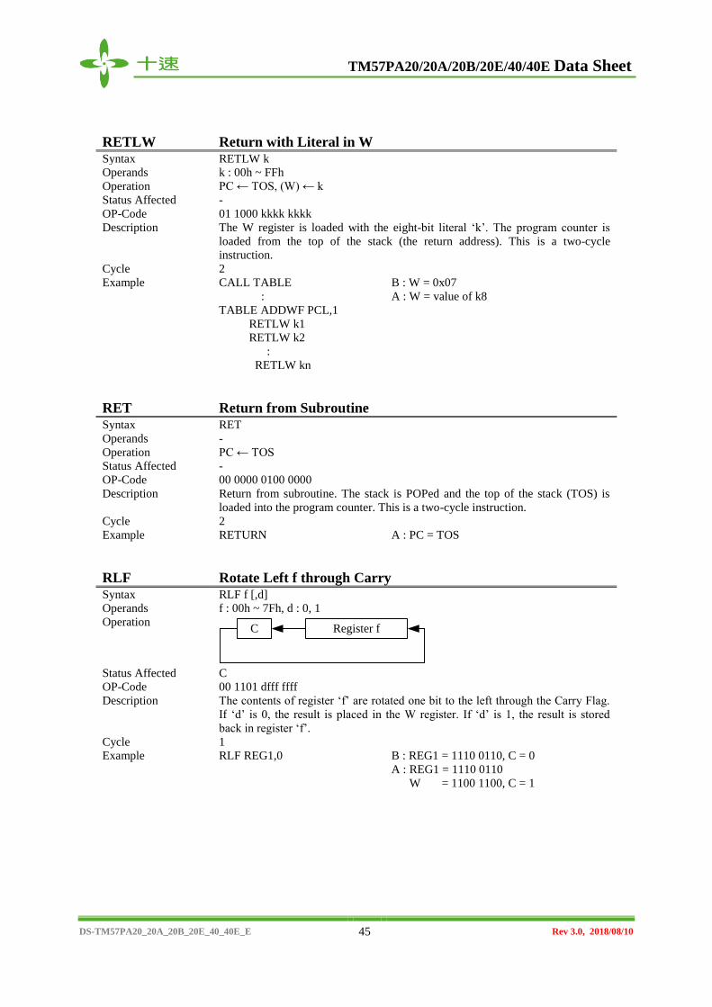
RETLW Return with Literal in W Syntax RETLW k
Operands k : 00h ~ FFh
Operation PC ← TOS, (W) ← k
Status Affected -
OP-Code 01 1000 kkkk kkkk
Description The W register is loaded with the eight-bit literal ‘k’. The program counter is
loaded from the top of the stack (the return address). This is a two-cycle
instruction.
Cycle 2
Example CALL TABLE
:
TABLE ADDWF PCL,1
RETLW k1
RETLW k2
:
RETLW kn
B : W = 0x07
A : W = value of k8
RET Return from Subroutine Syntax RET
Operands -
Operation PC ← TOS
Status Affected -
OP-Code 00 0000 0100 0000
Description Return from subroutine. The stack is POPed and the top of the stack (TOS) is
loaded into the program counter. This is a two-cycle instruction.
Cycle 2
Example RETURN A : PC = TOS
RLF Rotate Left f through Carry Syntax RLF f [,d]
Operands f : 00h ~ 7Fh, d : 0, 1
Operation C Register f
Status Affected C
OP-Code 00 1101 dfff ffff
Description The contents of register ‘f’ are rotated one bit to the left through the Carry Flag.
If ‘d’ is 0, the result is placed in the W register. If ‘d’ is 1, the result is stored
back in register ‘f’.
Cycle 1
Example RLF REG1,0 B : REG1 = 1110 0110, C = 0
A : REG1 = 1110 0110
W = 1100 1100, C = 1

TM57PA20/20A/20B/20E/40/40E Data Sheet
DS-TM57PA20_20A_20B_20E_40_40E_E 46 Rev 3.0, 2018/08/10
RRF Rotate Right “f” through Carry Syntax RRF f [,d]
Operands f : 00h ~ 7Fh, d : 0, 1
Operation C Register f
Status Affected C
OP-Code 00 1100 dfff ffff
Description The contents of register ‘f’ are rotated one bit to the right through the Carry Flag.
If ‘d’ is 0, the result is placed in the W register. If ‘d’ is 1, the result is placed
back in register ‘f’.
Cycle 1
Example RRF REG1,0 B : REG1 = 1110 0110, C = 0
A : REG1 = 1110 0110
W = 0111 0011, C = 0
SLEEP Go into standby mode, Clock oscillation stops Syntax SLEEP
Operands -
Operation -
Status Affected TO, PD
OP-Code 00 0000 0000 0011
Description Go into SLEEP mode with the oscillator stopped.
Cycle 1
Example SLEEP -
SUBWF Subtract W from “f” Syntax SUBWF f [,d]
Operands f : 00h ~ 7Fh, d : 0, 1
Operation (W) ← (f) – (W)
Status Affected C, DC, Z
OP-Code 00 0010 dfff ffff
Description Subtract (2’s complement method) W register from register ‘f’. If ‘d’ is 0, the
result is stored in the W register. If ‘d’ is 1, the result is stored back in register
‘f’.
Cycle 1
Example SUBWF REG1,1
SUBWF REG1,1
SUBWF REG1,1
B : REG1 = 3, W = 2, C = ?, Z = ?
A : REG1 = 1, W = 2, C = 1, Z = 0
B : REG1 = 2, W = 2, C = ?, Z = ?
A : REG1 = 0, W = 2, C = 1, Z = 1
B : REG1 = 1, W = 2, C = ?, Z = ?
A : REG1 = FFh, W = 2, C = 0, Z = 0
TM57PA20/20A/20B/20E/40/40E Data Sheet
DS-TM57PA20_20A_20B_20E_40_40E_E 47 Rev 3.0, 2018/08/10
SWAPF Swap Nibbles in “f” Syntax SWAPF f [,d]
Operands f : 00h ~ 7Fh, d : 0, 1
Operation (destination,7~4) ← (f.3~0), (destination.3~0) ← (f.7~4)
Status Affected -
OP-Code 00 1110 dfff ffff
Description The upper and lower nibbles of register ‘f’ are exchanged. If ‘d’ is 0, the result is
placed in W register. If ‘d’ is 1, the result is placed in register ‘f’.
Cycle 1
Example SWAPF REG, 0 B : REG1 = 0xA5
A : REG1 = 0xA5, W = 0x5A
TESTZ Test if “f” is zero Syntax TESTZ f
Operands f : 00h ~ 7Fh
Operation Set Z flag if (f) is 0
Status Affected Z
OP-Code 00 1000 1fff ffff
Description If the content of register ‘f’ is 0, Zero flag is set to 1.
Cycle 1
Example TESTZ REG1 B : REG1 = 0, Z = ?
A : REG1 = 0, Z = 1
XORLW Exclusive OR Literal with W Syntax XORLW k
Operands k : 00h ~ FFh
Operation (W) ← (W) XOR k
Status Affected Z
OP-Code 01 1111 kkkk kkkk
Description The contents of the W register are XOR’ed with the eight-bit literal ‘k’. The
result is placed in the W register.
Cycle 1
Example XORLW 0xAF B : W = 0xB5
A : W = 0x1A
XORWF Exclusive OR W with “f” Syntax XORWF f [,d]
Operands f : 00h ~ 7Fh, d : 0, 1
Operation (destination) ← (W) XOR (f)
Status Affected Z
OP-Code 00 0110 dfff ffff
Description Exclusive OR the contents of the W register with register ‘f’. If ‘d’ is 0, the result
is stored in the W register. If ‘d’ is 1, the result is stored back in register ‘f’.
Cycle 1
Example XORWF REG 1 B : REG = 0xAF, W = 0xB5
A : REG = 0x1A, W = 0xB5

TM57PA20/20A/20B/20E/40/40E Data Sheet
DS-TM57PA20_20A_20B_20E_40_40E_E 48 Rev 3.0, 2018/08/10
ELECTRICAL CHARACTERISTICS
1. Absolute Maximum Ratings
Parameter Rating Unit
Supply voltage VSS - 0.3 to VSS + 6.5
V Input voltage VSS - 0.3 to VDD + 0.3
Output voltage VSS - 0.3 to VDD + 0.3
Output current high per 1 PIN -25
mA Output current high per all PIN -80
Output current low per 1 PIN +30
Output current low per all PIN +150
Maximum Operating Voltage 5.5 V
Operating temperature -40 to +85 C
Storage temperature -65 to +150
TM57PA20/20A/20B/20E/40/40E Data Sheet
DS-TM57PA20_20A_20B_20E_40_40E_E 49 Rev 3.0, 2018/08/10
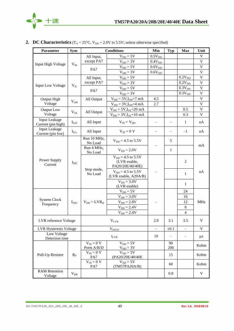
2. DC Characteristics (TA = 25°C, VDD = 2.0V to 5.5V; unless otherwise specified)
Parameter Sym Conditions Min Typ Max Unit
Input High Voltage VIH
All Input,
except PA7
VDD = 5V 0.5VDD V
VDD = 3V 0.4VDD V
PA7 VDD = 5V 0.6VDD V
VDD = 3V 0.6VDD V
Input Low Voltage VIL
All Input,
except PA7
VDD = 5V 0.2VDD V
VDD = 3V 0.2VDD V
PA7 VDD = 5V 0.3VDD V
VDD = 3V 0.3VDD V
Output High
Voltage VOH
All Output
VDD = 5V,IOH=7 mA 4.5 V
VDD = 3V,IOH=4 mA 2.7 V
Output Low
Voltage VOL All Output
VDD = 5V,IOL=20 mA 0.5 V
VDD = 3V,IOL=10 mA 0.3 V
Input Leakage
Current (pin high) IILH All Input VIN = VDD – – 1 uA
Input Leakage
Current (pin low) IILL All Input VIN = 0 V – – –1 uA
Power Supply
Current IDD
Run 10 MHz,
No Load VDD = 4.5 to 5.5V
–
5
mA Run 4 MHz,
No Load VDD = 2.0V 1
Stop mode,
No Load
VDD = 4.5 to 5.5V
(LVR enable,
PA20/20E/40/40E)
–
2
uA VDD = 4.5 to 5.5V
(LVR enable, A20A/B) 1
VDD = 3.0V
(LVR enable) 1
System Clock
Frequency fOSC VDD > LVRth
VDD = 5V
–
24
MHz
VDD = 3.0V 16
VDD = 2.8V 12
VDD = 2.4V 8
VDD = 2.4V 4
LVR reference Voltage VLVR 2.9 3.1 3.5 V
LVR Hysteresis Voltage VHYST – ±0.1 – V
Low Voltage
Detection time tLVR 10 – –
s
Pull-Up Resistor RP
VIN = 0 V
Ports A/B/D
VDD = 5V
VDD = 3V
90
200 Kohm
VIN = 0 V
PA7
VDD = 5V
(PA20/20E/40/40E 15 Kohm
VIN = 0 V
PA7
VDD = 5V
(TM57PA20A/B) 60 Kohm
RAM Retention
Voltage VDR 0.8 V
TM57PA20/20A/20B/20E/40/40E Data Sheet
DS-TM57PA20_20A_20B_20E_40_40E_E 50 Rev 3.0, 2018/08/10
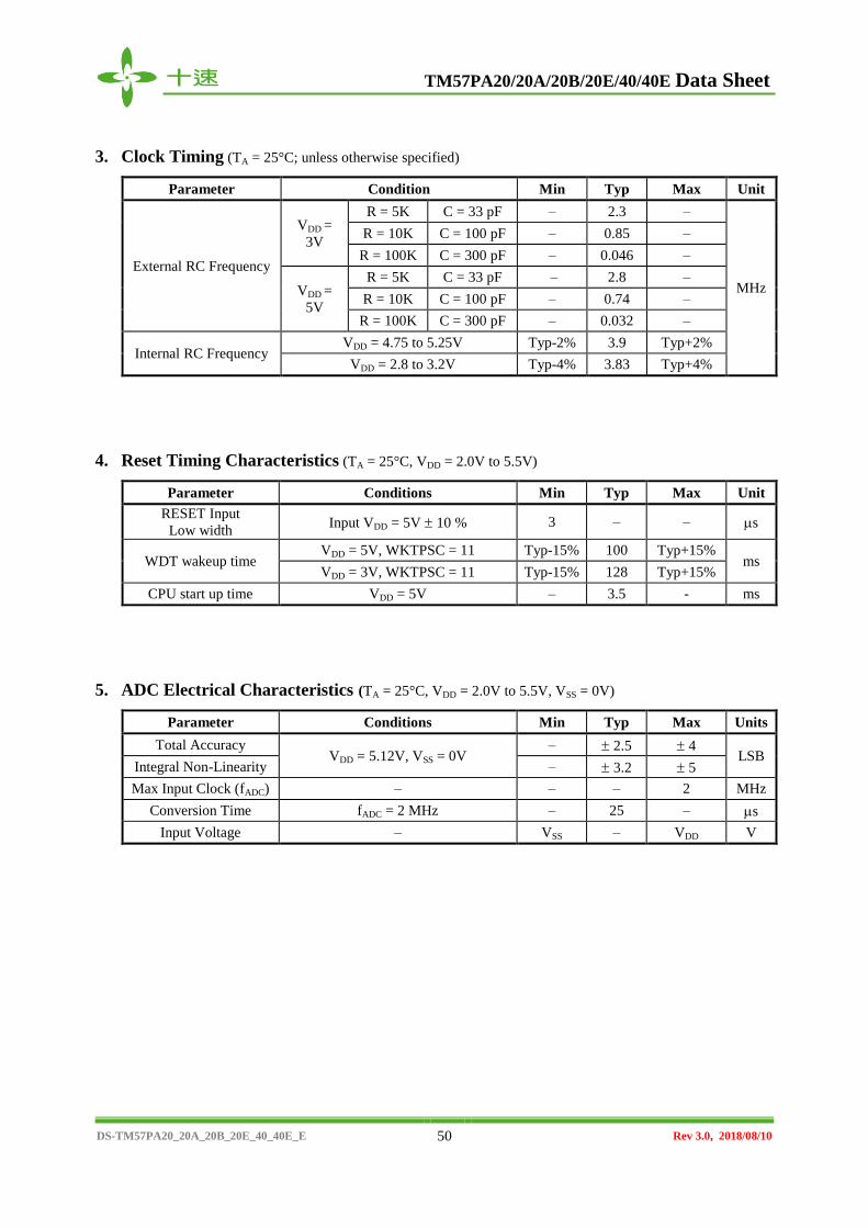
3. Clock Timing (TA = 25°C; unless otherwise specified)
Parameter Condition Min Typ Max Unit
External RC Frequency
VDD =
3V
R = 5K C = 33 pF – 2.3 –
MHz
R = 10K C = 100 pF – 0.85 –
R = 100K C = 300 pF – 0.046 –
VDD =
5V
R = 5K C = 33 pF – 2.8 –
R = 10K C = 100 pF – 0.74 –
R = 100K C = 300 pF – 0.032 –
Internal RC Frequency VDD = 4.75 to 5.25V Typ-2% 3.9 Typ+2%
VDD = 2.8 to 3.2V Typ-4% 3.83 Typ+4%
4. Reset Timing Characteristics (TA = 25°C, VDD = 2.0V to 5.5V)
Parameter Conditions Min Typ Max Unit
RESET Input
Low width Input VDD = 5V 10 % 3 – – s
WDT wakeup time VDD = 5V, WKTPSC = 11 Typ-15% 100 Typ+15%
ms VDD = 3V, WKTPSC = 11 Typ-15% 128 Typ+15%
CPU start up time VDD = 5V – 3.5 - ms
5. ADC Electrical Characteristics (TA = 25°C, VDD = 2.0V to 5.5V, VSS = 0V)
Parameter Conditions Min Typ Max Units
Total Accuracy VDD = 5.12V, VSS = 0V
– 2.5 4 LSB
Integral Non-Linearity – 3.2 5
Max Input Clock (fADC) – – – 2 MHz
Conversion Time fADC = 2 MHz – 25 – s
Input Voltage – VSS – VDD V

TM57PA20/20A/20B/20E/40/40E Data Sheet
DS-TM57PA20_20A_20B_20E_40_40E_E 51 Rev 3.0, 2018/08/10

TM57PA20/20A/20B/20E/40/40E Data Sheet
DS-TM57PA20_20A_20B_20E_40_40E_E 52 Rev 3.0, 2018/08/10
PACKAGING INFORMATION
The ordering information:
Ordering number Package
TM57PA20-OTP
TM57PA20A-OTP
TM57PA20B-OTP
TM57PA20E-OTP
TM57PA40-OTP
TM57PA40E-OTP
Wafer / Dice blank chip
TM57PA20-COD
TM57PA20A-COD
TM57PA20B-COD
TM57PA20E-COD
TM57PA40-COD
TM57PA40E-COD
Wafer / Dice with code
TM57PA20-OTP-03
TM57PA20A-OTP-03
TM57PA20B-OTP-03
TM57PA20E-OTP-03
TM57PA40-OTP-03
TM57PA40E-OTP-03
DIP 16-pin (300 mil)
TM57PA20-OTP-16
TM57PA20A-OTP-16
TM57PA20B-OTP-16
TM57PA20E-OTP-16
TM57PA40-OTP-16
TM57PA40E-OTP-16
SOP 16-pin (150 mil)
TM57PA20-OTP-05
TM57PA20A-OTP-05
TM57PA20B-OTP-05
TM57PA20E-OTP-05
TM57PA40-OTP-05
TM57PA40E-OTP-05
DIP 20-pin (300 mil)
TM57PA20-OTP-21
TM57PA20A-OTP-21
TM57PA20B-OTP-21
TM57PA20E-OTP-21
TM57PA40-OTP-21
TM57PA40E-OTP-21
SOP 20-pin (300 mil)
TM57PA20/20A/20B/20E/40/40E Data Sheet
DS-TM57PA20_20A_20B_20E_40_40E_E 53 Rev 3.0, 2018/08/10
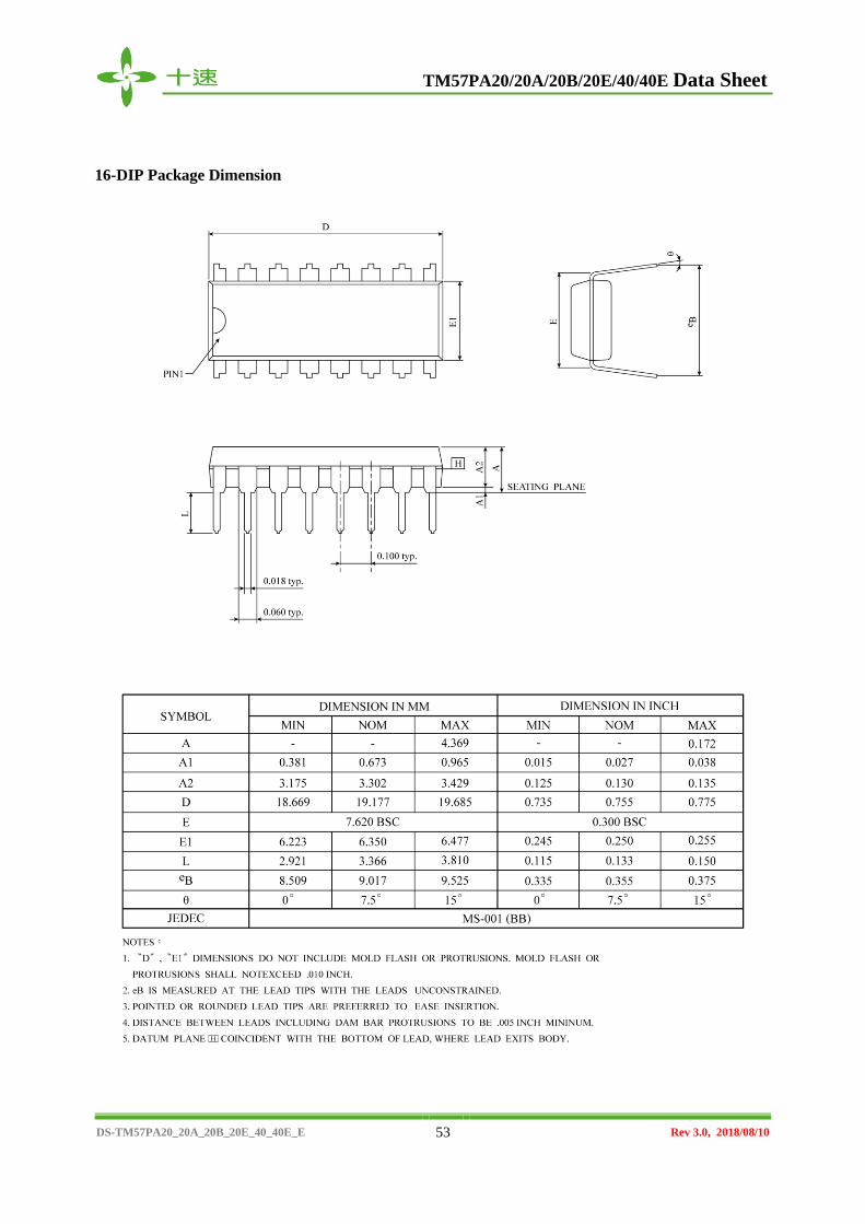
16-DIP Package Dimension
TM57PA20/20A/20B/20E/40/40E Data Sheet
DS-TM57PA20_20A_20B_20E_40_40E_E 54 Rev 3.0, 2018/08/10
16-SOP Package Dimension
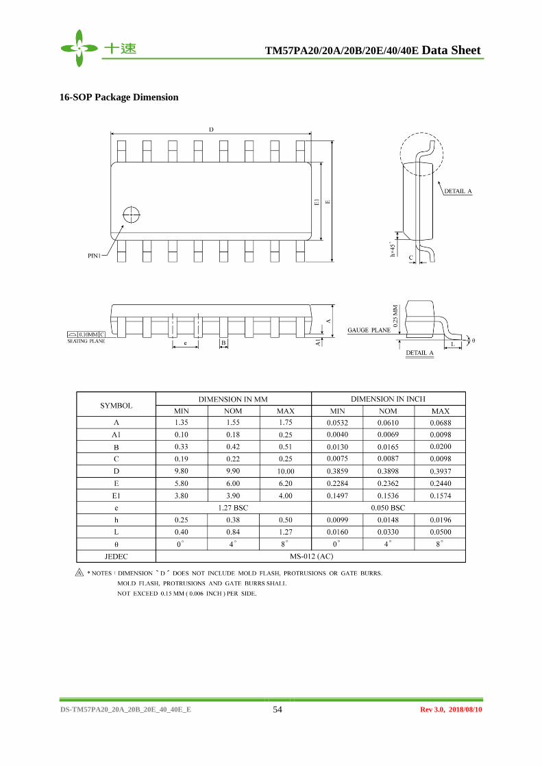
TM57PA20/20A/20B/20E/40/40E Data Sheet
DS-TM57PA20_20A_20B_20E_40_40E_E 55 Rev 3.0, 2018/08/10
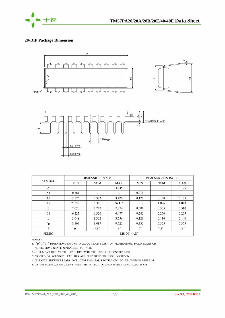
20-DIP Package Dimension
TM57PA20/20A/20B/20E/40/40E Data Sheet
DS-TM57PA20_20A_20B_20E_40_40E_E 56 Rev 3.0, 2018/08/10
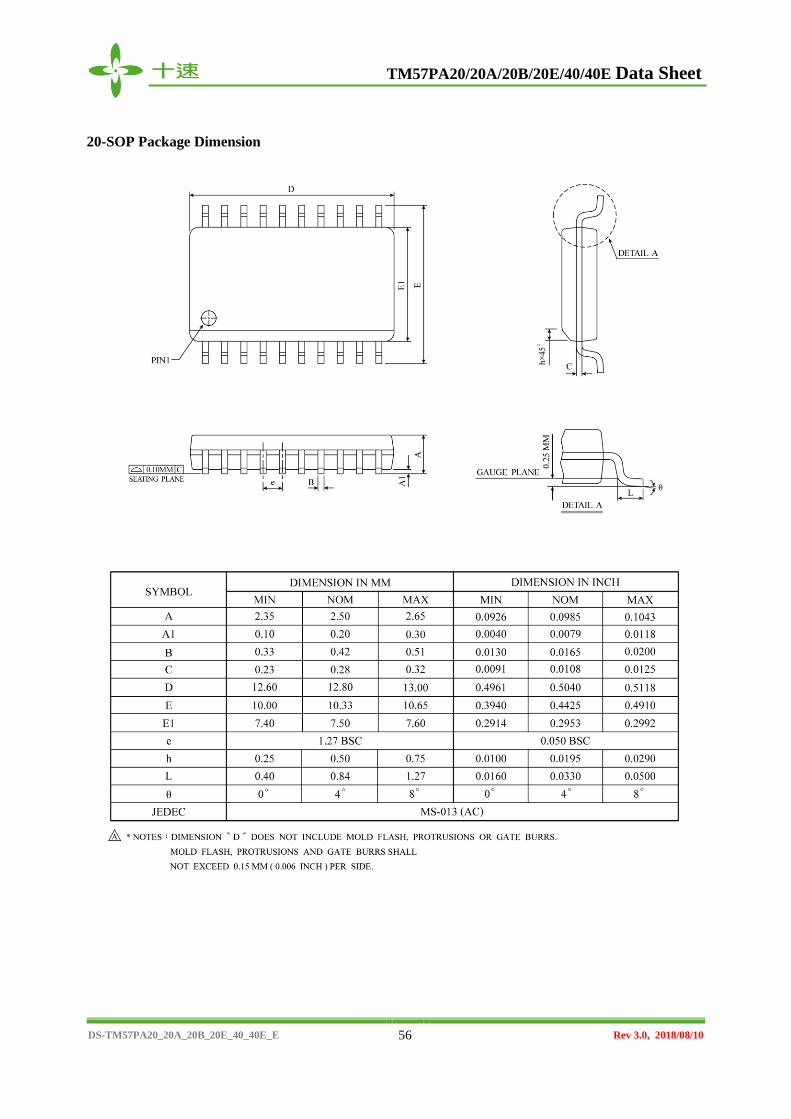
20-SOP Package Dimension