tm 11-5820-765-34
TRANSCRIPT

TM 11-5820-765-34
TM 11-5820-765-34

DO NOT TRY TO PULL OR GRAB THE lNDl-VIDUAL
IF YOU CANNOT TURN OFF THE ELECTRICALPOWER, PULL, PUSH, OR LIFT THE PERSON TOSAFETY USING A WOODEN POLE OR A ROPEOR SOME OTHER INSULATING MATERIAL
SEND FOR HELP AS SOON AS POSSIBLE
AFTER THE INJURED PERSON IS FREE OF CON-TACT WITH THE SOURCE OF ELECTRICALSHOCK, MOVE THE PERSON A SHORTDISTANCE AWAY AND IMMEDIATELY STARTARTIFICIAL RESUSCITATION

WARNING
L O W V O L T A G E , H I G H - A M P E R A G E C U R R E N T I S P R E S E N T A T O U T P U T C O N N E C T I O N S
A N D C O N N E C T I O N S I N S I D E E Q U I P M E N T .
SHUT OFF POWER SUPPLY BEFORE PERFORMING MAINTENANCE.
D I S C H A R G E C A P A C I T O R S B E F O R E P E R F O R M I N G T E S T S A N D M A I N T E N A N C E .
B E C A R E F U L W H E N W O R K I N G W I T H A C L I N E C O N N E C T I O N S .
SERIOUS INJURY OR DEATH MAY RESULT FROM CONTACT WITH TERMINALS.
DO NOT SERVICE OR ADJUST ALONE
Do not attempt internal service or adjustment unless another person, capable of rendering f irst
aid and resuscitation, is present.
SAFETY PRECAUTION
A periodic review of safety precautions in TB 385-4, Safety Precautions for Maintenance of Elec-
t r ica l /E lec t ron ic Equ ipment , is recommended. When the equipment is operated wi th coversremoved, DO NOT TOUCH exposed connections or components. MAKE CERTAIN you are not
grounded when making connections or adjusting components inside the test instrument.
TRICHLOROTRIFLUOROETHANE
Adequate venti lat ion should be provided while using TRICHLOROTRIFLUOROETHANE. Prolonged
breathing of vapor should be avoided. The solvent should not be used near heat or open flame;
the products o f decomposi t ion are tox ic and i r r i ta t ing. Since’ TRICHLOROTRIFLUOROETHANE
dissolves natural oi ls, prolonged contact with skin should be avoided. When necessary, use
gloves which the solvent cannot penetrate. If the solvent is taken internally, consult a physician
i m m e d i a t e l y .
PROTECTIVE COATING EC1103 IS TOXIC.USE PROPER VENTILATION: AVOID BREATHING FUMES.
AVOID CONTACT WITH SKIN.
HEAVY EQUIPMENT
Don’t take chances. Avoid personal injury. These equipments are heavy. They weigh 100-125
pounds. Use four persons to lift.
A / ( B B L A N K )

TECHNICAL MANUAL
NO. 11-5820-765-34
* TM 11-5820-765-34
HEADQUARTERS
DEPARTMENT OF THE ARMY
Washington, DC, 15 August 1983
DIRECT SUPPORT AND GENERAL SUPPORTMAINTENANCE MANUAL
POWER SUPPLIES
PP-4763/GRC (NSN 5820-00-937-7690)AND
PP-4763A/GRC (NSN 5820-00-113-9768)
REPORTING ERRORS AND RECOMMENDING lMPROVEMENTS
You can help improve this manual. If you find any mistakes or if you know of a
way to improve the procedures, please let us know. Mail your letter, DA Form
2028 (Recommended Changes to Publications and Blank Forms), or DA Form
2 0 2 8 - 2 l o c a t e d i n b a c k o f t h i s m a n u a l d i r e c t t o : C o m m a n d e r , U S A r m y
Communications-Electronics Command and Fort Monmouth, ATTN: DRSEL-ME-
MP, Fort Monmouth, New Jersey 07703. A reply will be furnished direct to you.
T A B L E O F C O N T E N T S
CHAPTER 1
Sect ion I
Sect ion I I
Sect ion I I I
C H A P T E R 2
Sect ion I
Sect ion I I
Sect ion I I I
S e c t i o n I V
C H A P T E R 3
INTRODUCTION . . . . . . . . . . . . . . . . . . . . . . . . . . . . . . . . . . . . . . . . . . .
Sect ion I
Sect ion I I
Sect ion I I I
S e c t i o n I V
APPENDIX A
P A G E
1-0
1-2
1-2
1-5
2-0
2-1
2-2
2-22
2-44
3-1
3-2
3-3
3-6
3-10
A-1
A P P E N D I X B EXPENDABLE SUPPLIES AND MATERIALS LIST. . . . . . . . . . . . . . . . . . . . B-1
INDEX . . . . . . . . . . . . . . . . . . . . . . . . . . . . . . . . . . . . . . . . . . . . . . . . . . . . . . . . . . . . . . . . . Index-1
FOLDOUT INDEX . . . . . . . . . . . . . . . . . . . . . . . . . . . . . . . . . . . . . . . . . . . . . . . . . . . . . . . F o l d o u t I n d e x - 1
*Th i s manua l supe rsedes TM 11 -5820 -765 -35 , 15 June 1969 .
i

TM 11-5820-765-34
1-0

TM 11-5820-765-34
CHAPTER 1
I N T R O D U C T I O N
S e c t i o n I . G E N E R A L I N F O R M A T I O N
P A G E
Destruction of Army Materiel to Prevent Enemy Use . . . . . . . . . . . . . . . . . . . . . . . . . . . . . . 1-2Maintenance Forms, Records and Reports . . . . . . . . . . . . . . . . . . . . . . . . . . . . . . . . . . . . . 1-2
Reporting Equipment improvement Recommendations (ElR) . . . . . . . . . . . . . . . . . . . . . . . 1-2Scope . . . . . . . . . . . . . . . . . . . . . . . . . . . . . . . . . . . . . . . . . . . . . . . . . . . . . . . . . . . . . . . . . . . . . 1-2Technical Characteristics . . . . . . . . . . . . . . . . . . . . . . . . . . . . . . . . . . . . . . . . . . . . . . . . . . . . 1-2
S e c t i o n I I . E Q U I P M E N T D E S C R I P T I O N A N D D A T A
Differences Between Models. . . . . . . . . . . . . . . . . . . . . . . . . . . . . . . . . . . . . . . . . . . . . . . . . 1-3PowerSupplyConnectionsto Radio Set AN/GRC-106 . . . . . . . . . . . . . . . . . . . . . . . . . . . . . 1-4
Purpose and Use . . . . . . . . . . . . . . . . . . . . . . . . . . . . . . . . . . . . . . . . . . . . . . . . . . . . . . . . . . . 1-2
Safety, Care, and Handling . . . . . . . . . . . . . . . . . . . . . . . . . . . . . . . . . . . . . . . . . . . . . . . . . . . 1-4
S e c t i o n I I I . T E C H N I C A L P R I N C I P L E S O F O P E R A T I O N
Block Diagram Analysis . . . . . . . . . . . . . . . . . . . . . . . . . . . . . . . . . . . . . . . . . . . . . . . . . . . . . . 1-5
Control Circuits . . . . . . . . . . . . . . . . . . . . . . . . . . . . . . . . . . . . . . . . . . . . . . . . . . . . . . . . . . . . 1-8
Powerand Voltage Circuits. . . . . . . . . . . . . . . . . . . . . . . . . . . . . . . . . . . . . . . . . . . . . . . . . . . 1-6
1-1

TM 11-5820-765-34
Section I. GENERAL INFORMATION
1 - 1 . S C O P E
This manual descr ibes d i rec t and genera l suppor t main tenance for Power Supply PP-4763/GRC
and Power Supp ly PP-4763A/GRC. I t inc ludes ins t ruc t ions for t roub leshoot ing, repa i r ing , and
test ing the equipment . I t a lso l is ts a l l the too ls , tes t equ ipment , and mater ia ls needed for
m a i n t e n a n c e .
The power supplies and their maior electronic components are described in section II of this chapter.
Operating instructions and organizational maintenance are covered in TM 11-5820-765-12.
N O T E
In th is manual , Power Suppl ies PP-4763/GRC and PP-4763A/GRC are re fer -
r e d t o a s p o w e r s u p p l y ( * ) . S p e c i f i c m o d e l s a r e i d e n t i f i e d b y u n i t
n o m e n c l a t u r e , w i t h o u t t h e G R C d e s i g n a t i o n .
1-2. MAINTENANCE FORMS, RECORDS, AND REPORTS
Department of the Army forms and procedures used for equipment maintenance wil l be those prescribed
by TM 38-750, The Army Maintenance Management System (TAMMS).
1-3. DESTRUCTION OF ARMY MATERIEL TO PREVENT ENEMY USE
Dest ruc t ion o f Army e lec t ron ics mater ie l to prevent enemy use sha l l be in accordance wi th TM
750-244-2.
1 - 4 . R E P O R T I N G E Q U I P M E N T I M P R O V E M E N T R E C O M M E N D A T I O N S ( E I R )
If your Power Supplies PP-4763/GRC and PP-4763A/GRC need improvement, let us know. Send us an
EIR. You, the user, are the only one who can tell us what you don’t like about your equipment. Let us
know why you don’t like the design. Put it on an SF 368 (Quality Deficiency Report). Mail it to Com-
mander, US Army Communications-Electronics Command and Fort Monmouth, ATTN: DRSEL-ME-MP,
Fort Monmouth, New Jersey 07703. We’ll send you a reply.
1 - 5 . T E C H N I C A L C H A R A C T E R I S T I C S
See TM-11-5820-765-12, paragraph 1-5.
Section II. EQUIPMENT DESCRIPTION AND DATA
1-6. EQUIPMENT CHARACTERISTICS, CAPABILITIES AND FEATURES
The power supp l ies funct ion in the same way. Both prov ide a dc power source for communica-
t ions equipment , or for any type of load wi th s imi lar power requ i rements .
PP-4763 conver ts 115 vo l ts a l te rnat ing cur rent (a t ) to d i rec t cur rent (de) a t a se lec ted regu la ted
v o l t a g e .
PP-4763A converts either 115 or 230 volts alternating current (at) to direct current (de) at a
s e l e c t e d r e g u l a t e d v o l t a g e .
1-2

TM 11-5820-765-34
1 - 7 . D I F F E R E N C E S B E T W E E N M O D E L S
Differences Between Parts
Item PP-4763 PP-4763A
A C p o w e r o p t i o n
AC power cab le W3
AC power sw i tch CB1
D C o u t p u t c o n n e c t i o n s
Termina l board TB1
Reactor L3 (choke)
T o p c o v e r i n t e r l o c k s w i t c h
S1
Test jacks (on c i rcu i t card
a s s e m b l y )
115 vo l ts ac ,
Prov ided wi th terminal lug for
each wi re connect ion to ac
p o w e r s o u r c e .
S ing le swi tch c i rcu i t b reaker .
T e r m i n a l b o a r d A 8 - c a b l e
a t t a c h e d t o c o n n e c t d c o u t p u t
t o e q u i p m e n t u n d e r t e s t .
P r o v i d e s c o n n e c t i o n s f o r
t r a n s f o r m e r T 1 .
N o t p r o v i d e d
N o t p r o v i d e d
N o t p r o v i d e d
115 or 230 volts ac,
63 Hz.
P r o v i d e d w i t h l o c k i n g p r o n g s
on p lug for connect ion to ac
p o w e r s o u r c e .
D o u b l e s w i t c h c i r c u i t b r e a k e r .
C a b l e f r o m e q u i p m e n t u n d e r
t e s t c o n n e c t e d e i t h e r t o
termina l board A8 or to
receptac le J1 .
P r o v i d e s c o n n e c t i o n s f o r
t ransformer T-1 and for 115-
vo l t ac /230-vo l t ac I inks .
P r o v i d e d
P r o v i d e d ; d i s c o n n e c t s a c i n p u t
power when top cover is
r e m o v e d .
Test jacks TP1 th rough TP6
p r o v i d e d .
Differences Between Reference Designations
Most par ts used in both power suppl ies have one re ference des ignat ion.
E X A M P L E :V o l t m e t e r i s d e s i g n a t e d M l i n b o t h p o w e r s u p p l i e s .
T h e f o l l o w i n g p a r t s h a v e d i f f e r e n t r e f e r e n c e d e s i g n a t i o n s :
PP-4763 P P - 4 7 6 3 A
C i r c u i t c a r d a s s e m b l y PC101 A1
R e c t i f i e r b r i d g e z N o d e s i g n a t i o n
(on c i rcu i t card assembly)
RFI f i l ter F L z
S i l i c o n c o n t r o l l e d r e c t i f i e r S C R Q
For these par ts , parentheses ind ica te des ignat ions for PP-4763A.
E X A M P L E :
Ci rcu i t card assembly appears in tex t as PC101(A1) .
1-3

1-9.
TM 11-5820-765-34
W A R N I N G
HEAVY EQUIPMENT
Don’t take chances. Avoid personal injury. These equipments are heavy. They weigh 100-125 pounds.
Use four persons to lift.
1-8 . SAFETY, CARE, AND HANDLING
Be careful when lifting the equipment. PP-4763 weighs 120 pounds and PP-4763A weighs 125
pounds. When packed for shipment, each unit weighs about 200 pounds.
Use four persons to remove unit from shelter.Carry by both handles at all times.
Read all WARNINGS, CAUTIONS, and NOTES. Think safety!
1 - 4

TM 11-5820-765-34
Section III. TECHNICAL PRINCIPLES OF OPERATION
1 - 1 0 . B L O C K D I A G R A M A N A L Y S I S
The b lock d iagram descr ibes the power sup-
p l y ’ s m a j o r e l e c t r o n i c c o m p o n e n t s a n d c i r c u i t s .
The power supply requires an input of 115
volts ac or 230 volts ac for operation, and has an
output o f 27-29 vo l ts dc .
Input power: Appl ied through a rad io f requen-
cy in ter fe rence (RFI ) f i l te r to the c i rcu i t b reaker .
Wi th the c i rcu i t b reaker c losed (POWER ON) ,input power f lows to the power t ransformer ,
wh ich feeds the fan motor , c i rcu i t card
assembly , and a l l o f the power supp ly ’s c i rcu i ts .
O u t p u t : T h e t r a n s f o r m e r a p p l i e s p o w e r
through a reactor to a fu l l -wave br idge rect i f ie r ,
wh ich conver ts the input f low to dc . A s i l i con
cont ro l led rect i f ie r regu la tes the dc output ; con-
t ro l c i rcu i t ry in the c i rcu i t card assembly pro-
v i d e s a u t o m a t i c , c o n t i n u o u s v o l t a g e r e g u l a t i o n .
A f i l te r network pur i f ies the dc s igna l ; the
regu la ted pos i t ive dc output f lows through the
output cur rent meter (ammeter ) and is shunt to
t h e d c o u t p u t t e r m i n a l .
A vo l tage ad just c i rcu i t permi ts manual ad just -
ment o f the output vo l tage; cont ro ls in the c i r -
cu i t card assembly sense the ad jus tment and
change the vol tage.
An overvo l tage c i rcu i t , ac t iva ted when needed,
appl ies a shor t -c i rcu i t load to the output ter -
mina ls , opening the c i rcu i t breaker . Th is pro-
tects the power supply and the equipment being
p o w e r e d .
The output vo l tage meter (vo l tmeter ) moni tors
output vo l tage, wh ich passes aga in through the
RFI f i l te r before reaching the dc output termina l .
1-5

TM 11-5820-765-34
1 - 1 1 . P O W E R A N D V O L T A G E C I R C U I T S
POWER CIRCUITS
PP-4763
CIRCUIT BREAKER CB1 ( re fe r to FO-2) :
Single ac power switch.
Turns power supp ly ON, OFF.
Pro tec ts aga ins t over load ing power supp ly .
Power ON: Connects 115-vo l t ac source to pr imary w ind ing, power t rans former T-1 ,
and to fan motor B1.
PP-4763A
CIRCUIT BREAKER CB1 ( re fe r to FO-3) :
Dual ac power switch.
Turns power supp ly ON, OFF.
In ser ies w i th both legs o f ac input power .
Power ON: Connects e i ther 115-or 230-vo l t ac source to pr imary wind ing, power
t ransformer T1, and to fan motor B1.
S A F E T Y I N T E R L O C K S W I T C H S 1 :
Opens input power c i rcu i t when un i t ’s top pane l is removed.
This is a protective control.
Functional Analysis of Power Circuit Parts
T R A N S F O R M E R T 1 :
S e c o n d a r y w i n d i n g :
Power secondary supp l ies fu l l -wave br idge rec t i f ie r
(rectif ier diodes CR1, CR2, CR3, and CR4).
Two cont ro l secondar ies supp ly c i rcu i t card assembly PC101 (A l ) .
S IL ICON CONTROLLED RECTIFIER SCR1 (Q1) :
Connected in bridge rectifier outlet.
Regulates dc output.
R E A C T O R L 2 :
Connected in ac supply to bridge rectifier.
Introduces time delay needed to operate SCR1 (Q1).
DIODE CR5:
Connected across bridge rectifier’s output.
Prov ides d ischarge path fo r f i l te r reactor L1.
Prevents continued firing of SCR1 (Q1).
BLEEDER RESISTORS R1, R10:
Connected across bridge rectifier’s output.
Stab i l ize power supply ’s operat ions dur ing low- load condi t ions.
PP-4763A inc ludes choke L3 in ser ies w i th R10.
1-6

TM 11-5820-765-34
VOLTAGE SURGE PROTECTOR DIODE CR6:
C o n n e c t e d a c r o s s t r a n s f o r m e r ’ s p o w e r s e c o n d a r y w i n d i n g .
Pro tec ts vo l tage regu la tor rec t i f ie r SCR1 (Q1) and br idge rec t i f ie r d iodes CR1-CR4 f rom
t r a n s i e n t v o l t a g e s p i k e s .
VOLTAGE REGULATION CIRCUIT
Bui l t in to c i rcu i t card assembly PC101 (A1) .
Cont ro ls f i r ing t ime o f s i l i con cont ro l led rec t i f ie r SCR1 (Q1) .
Keeps dc vo l tage a t ad jus ted set t ing .
E X P L A N A T I O N :
SCR1 (Q1) f i res tw ice each cyc le o f ac input vo l tage. By cont ro l l ing f i r ing t ime, SCR1 (Q1)
can be var ied f rom fu l l on when f i red a t s tar t o f each ha l f -cyc le to fu l l o f f when f i red
at end o f ha l f -cyc le .
Br idge rec t i f ie r ’s dc output vo l tage can thus be var ied f rom maximum poss ib le vo l tage to
zero .
OVERVOLTAGE CIRCUIT
CIRCUIT PARTS:
Si l i con cont ro l led rec t i f ie r SCR2 (Q2) .
Low-res is tance res is to r R3.
P r o t e c t s e q u i p m e n t b e i n g p o w e r e d f r o m o v e r v o l t a g e s .
Act iva ted when mal funct ion causes r ise in output vo l tage.
A C T I O N :
Circuitry in PC101 (A1) senses trouble, f ires SCR2 (Q2).
R E S U L T S :
F i r ing app l ies shor t -c i rcu i t load to output termina ls which reduces output vo l tage to very
low va lue.
Short-circuit load opens circuit breaker CB1, which turns power supply OFF.
This prevents possible damage to power supply and equipment being pawered.
VOLTAGE ADJUST CIRCUIT (DC OUTPUT)
CIRCUIT PARTS:
Var iab le dc vo l tage ad jus t res is tors R4, R8.
Stabilizing capacitor C3.
Fixed resistor R11.
C O N N E C T I O N :
Do output vo l tage fed through res is tors to PC101(A1) .
V O L T A G E P A T H :
Do output negative (–) terminal to PC101 (A1).
A d j u s t s p o w e r s u p p l y ’ s d c o u t p u t v o l t a g e .
A c t i v a t e d w h e n d c o u t p u t v o l t a g e c h a n g e s .
1-7

TM 11-5820-765-34
A C T I O N :
Manual ly ad just dc vo l tage ad just R4.
Resistors R4, R8 change setting.
Cont ro l c i rcu i t ry in PC101(A1) senses change.
R E S U L T S :
O u t p u t v o l t a g e c h a n g e s p r o p o r t i o n a l l y .
R E S I S T O R F U N C T I O N S :
R4 adjusts output vo l tage.
R8 adjusts voltage range.
1 - 1 2 . C O N T R O L C I R C U I T S
CIRCUIT CARD ASSEMBLY PC101(A1) :
C o n t r o l s p o w e r s u p p l y o p e r a t i o n .
Senses vo l tage changes in ac input , dc output c i rcu i ts .
Cont ro ls opera t ion o f vo l tage regu la t ion , overvo l tage c i rcu i ts .
Der ives power f rom two secondary w ind ings on t rans former T1.
VOLTAGE REGULATION CONTROL
P C 1 0 1 ( A 1 ) C O N N E C T S T O :
S i l i c o n c o n t r o l l e d r e c t i f i e r S C R 1 ( Q 1 ) .
Power supp ly ’s f ina l dc output vo l tage.
N O T E
SCR1(Q1) regu la tes dc output vo l tage.
A C T I O N :PC101 (A1) applies signal to SCR1 (Q1) gate.
SCR1(Q1) f i res , conducts cur ren t a f te r rece iv ing s igna l .
T iming of cont ro l gate s ignal appears on gate.
T I M I N G :
Timing of cont ro l gate s igna l depends on va lue of output vo l tage fed to PC101(A1) .
IF : Do output vo l tage increases
THEN: T ime constants in PC101(A1) de lay f i r ing SCR1(Q1)
SO: SCR1(Q1) f ires later in half-cycle
W H I C H : R e d u c e s o u t p u t v o l t a g e
This res tores output vo l tage to proper va lue.
IF: Do output vo l tage decreases
THEN: SCR1(Q1) f i res ear ly
WHICH: Ra ises vo l tage to proper va lue.
First Power Supply to PC101(A1)
P O W E R :
Plus and minus 20 volts.
1-8

TM 11-5820-765-34
S O U R C E :
C e n t e r - t a p p e d s e c o n d a r y w i n d i n g , t r a n s f o r m e r T 1 .
RECTIFIER BRIDGE CIRCUIT:
PP-4763 Rectifier bridge Z 102.
PP-4763A Individual divides CR18, CR19, CR20, CR21.
DC OUTPUT Z108 (CR18-CR21):
F I L T E R :
Resistor-capasitor filter circuit R102(R2); C103(C3); R103(R3); C104(C4).
R E G U L A T O R :
Resistor R105(R5)
Zener diodes CR109(CR9); CR110(CR10).
PLUS-MINUS 20-VOLT SUPPLY CIRCUIT:
C o m m o n p o i n t c o n n e c t s t o p o w e r s u p p l y ’ s p o s i t i v e o u t p u t .
PLUS 20-VOLT CIRCUIT:
Suppl ies re ference d iode CR104(CR4) th rough res is tor R113(R13) .
Output o f CR104(CR4) prov ides b ias cur rent to base o f t rans is tor Q103(Q3) .
MINUS 20-VOLT CIRCUIT:
Supp l ies vo l tage d iv ider R107(R7) , R115(R15) , t ransmi t te r - res is tor c i rcu i t Q103(Q3) ,
R117(R17).
Second Power Supply to PC101(A1)
S O U R C E :
Transformer T1, windings TB1-11, TB1-10.
Cur rent passes th rough cur rent - l im i t ing res is tors R6, R7.
RECTIFIER BRIDGE CIRCUIT:
PP-4763 - Rectifier bridge Z101.
PP-4763A - Diodes CR14, CR15, CR16, CR17.
PULSATING DC OUTPUT, Z101 (CR14-CR17) :
Clipped by Zener diode CR109(CR9) through blocking diode CR105(CR5).
Circuit output supplies:
Res is tor -un i junc t ion t rans is tor c i rcu i t R108(R8) , R109(R9) , Q101(Q1) .
Resistor-transistor circuit R1 11(R11), R112(R12), Q102(Q2).
P O W E R S U P P L Y ’ S O U T P U T V O L T A G E :
A p p l i e d t h r o u g h f r o n t p a n e l m o u n t e d a d j u s t m e n t a s s e m b l y A 4 A 2 A 1 R 1 1 , A 4 A 2 R 4 a n d
A4A2R8, th rough res is tor R120(R20) , to base o f t rans is tor Q103(Q3) .
Base cur rent Q103(Q3) c reates cur rent th rough R117(R17) .
Cur rent c reates b ias vo l tage fo r base o f Q102(Q2) .
Th is c reates cur rent f low through res is tors R111(R11) , R112(R12) .
Th is supp l ies capac i to r C105(C5) .
C105(C5) connects th rough b lock ing d iode CR112(CR12) to emi t te r o f un i junct ion
t rans is to r Q101(Q1) .
1-9

T M 1 1 - 5 8 2 0 - 7 6 5 - 3 4
Functional Description of PC101(A1) Power Supply Circuits
Vol tage o f a l l secondary w ind ings in t ransformer T1 becomes zero a t same ins tant . A t
t h i s i n s t a n t :
Anode- to-cathode vo l tage o f cont ro l led rec t i f ie r SC R1(Q1) a lso becomes zero and shuts
O F F .
As anode- to-ca thode vo l tage r ises , SC R1(Q1) s tays OFF unt i l PC101(A1) supp l ies s igna l to
g a t e .
Cl ipped pu lsat ing vo l tage to un i junct ion t rans is tor Q101(Q1) a lso becomes zero a t th is ins-
t a n t .
Vo l tage to vo l tage d iv ider R108, R109(R8, R9) bu i lds to maximum va lue in approx imate ly
0 . 3 m i l l i s e c o n d .
Vol tage to base 2-base 1 c i rcu i t o f Q101(Q1) bu i lds to maximum va lue in 0 .3 mi l l i second.
Vol tage to emi t ter Q101(Q1) bu i lds s lowly , due to charg ing t ime of capac i tor C105(C5) .
Emitter-base 1 resistance decreases, which connects C105(C5) to:
res is to r R109(R9) ,
gate o f cont ro l led rec t i f ie r SCR101(Q6) .
SC R101(Q6) turns on.
Connects output o f rec t i f ie r b r idge Z102(CR18 through CR21) to gate o f SCR1(Q1) .
SC R1(Q1) turns on.
Results of Voltage Changes
Act ion descr ibed above occurs tw ice per cyc le (120 t imes/second wi th 60 Hz input ) .
SC R1(Q1) is fired at same instant of each cycle.
IF : Output vo l tage changes (due to change in ac input vo l tage or dc output
v o l t a g e ) .
THEN: Base cur ren t o f t rans is to r Q103(Q3) changes.
WHICH: Changes cur rent th rough R117(R17) .
WHICH: Changes base vo l tage o f t rans is tor Q102(Q2) .
IF : Output vo l tage increases.
THEN: Base vo l tage o f Q102(Q2) increases.
WHICH: Increases cur rent th rough R111(R11) .
WHICH: Reduces charg ing cur rent in to capac i to r C105(C5) .
WHICH: De lays f i r ing t ime o f un i junc t ion t rans is tor Q101(Q1) .
WHICH: De lays f i r ing o f SCR1(Q1) .
IF: SCR1(Q1) f ires later in each half-cycle.
T H E N : O u t p u t v o l t a g e r e d u c e d .
WHICH: Restores output vo l tage to proper va lue.
OVERVOLTAGE CONTROL
O V E R V O L T A G E C I R C U I T :
Components: Silicon controlled rectifier SCR2 (Q2).
Connected in series across dc output.
C O N N E C T I O N S T O C O N T R O L C I R C U I T :
Gate o f SCR2 (Q2) connected to cont ro l c i rcu i t in PC101 (A1) .
Cont ro l c i rcu i t connected to pos i t i ve (+) , negat ive (–) dc output te rmina ls .
1-10

TM 11-5820-765-34
S E Q U E N C E :
Vol tage r ises above prescr ibed va lue.
Signal applied to gate of SCR2 (Q2).
SCR2 (Q2) conducts.
Shorts output.
Opens circuit breaker CB1.
CONTROL CIRCUIT
V O L T A G E D I V I D E R :
Resistors R121, R122, R123 (R21, R22, R23).
Connected across dc output terminals.
R E G U L A T O R D I O D E C I R C U I T :
Regulator diode CR106 (CR6).
Resistor R124 (R24).
Transistor Q104 (Q4).
Supp l ies gate o f s i l i con cont ro l led rec t i f ie r SCR2 (Q2) th rough l im i t ing res is tor R125 (R25) .
TRANSISTOR Q104 (Q4) :
Compares por t ion o f output vo l tage wi th vo l tage of CR106 (CR6) .
N O T E
Por t ion o f vo l tage compared depends on set t ing o f var iab le res is tor R123
(R23).
IF : Output vo l tage r ises above preset va lue.
THEN: Q104 (Q4) conducts .
WHICH: F i res SCR2 (Q2) .
WHICH: Opens c i rcu i t b reaker CB1.
CAPACITOR C108 (C8) :
Stabilizes operation.
Insures against short t ime transients f ir ing SCR2 (Q2).
1-11

TM 11-5820-765-34
C H A P T E R 2
D I R E C T S U P P O R T M A I N T E N A N C E
S e c t i o n I . G E N E R A L I N F O R M A T I O N
S e c t i o n I I . T R O U B L E S H O O T I N G
Adjusting Voltage Control Circuits . . . . . . . . . . . . . . . . . . . . . . . . . . . . . . . . . . . . . . . . . . . .
Component Testing . . . . . . . . . . . . . . . . . . . . . . . . . . . . . . . . . . . . . . . . . . . . . . . . . . . . . . . . .
Procedures . . . . . . . . . . . . . . . . . . . . . . . . . . . . . . . . . . . . . . . . . . . . . . . . . . . . . . . . . . . . . . . .
Symptom Index . . . . . . . . . . . . . . . . . . . . . . . . . . . . . . . . . . . . . . . . . . . . . . . . . . . . . . . . . . . . .
Testing and Troubleshooting Circuit Card Assembly PC101(A1) . . . . . . . . . . . . . . . . . . . .
Troubleshooting Chart . . . . . . . . . . . . . . . . . . . . . . . . . . . . . . . . . . . . . . . . . . . . . . . . . . . . . . .
Voltage and Resistance Data.. . . . . . . . . . . . . . . . . . . . . . . . . . . . . . . . . . . . . . . . . . . . . . . .
S e c t i o n I I I . M A I N T E N A N C E P R O C E D U R E S
Removing and Replacing Panels . . . . . . . . . . . . . . . . . . . . . . . . . . . . . . . . . . . . . . . . . . . . . .
Removing and Replacing Parts: . . . . . . . . . . . . . . . . . . . . . . . . . . . . . . . . . . . . . . . . . . . . . . .
AC cable plug W3P1 . . . . . . . . . . . . . . . . . . . . . . . . . . . . . . . . . . . . . . . . . . . . . . . . . . . . . . .
AC cable W3 . . . . . . . . . . . . . . . . . . . . . . . . . . . . . . . . . . . . . . . . . . . . . . . . . . . . . . . . . . . . .
AC input links . . . . . . . . . . . . . . . . . . . . . . . . . . . . . . . . . . . . . . . . . . . . . . . . . . . . . . . . . . . .
Ammeter Ma . . . . . . . . . . . . . . . . . . . . . . . . .
Capacitors C1, C2 . . . . . . . . . . . . . . . . . . . . .
Circuit breaker CB1 . . . . . . . . . . . . . . . . . . .
Circuit card assembly PC101(A1) . . . . . . . .
DCvol tagead jus t components R4, R8, R11,
Diodes CR1-CR5 . . . . . . . . . . . . . . . . . . . . . .
Diode CR6 . . . . . . . . . . . . . . . . . . . . . . . . . . . .
Diode SCR1 (Q1) . . . . . . . . . . . . . . . . . . . . . . . . . . . . . . . . . . . . . . . . . . . . . . . . . . . . . . . . . .
Diode SCR2 (Q2) . . . . . . . . . . . . . . . . . . . . . . . . . . . . . . . . . . . . . . . . . . . . . . . . . . . . . . . . . .
FanmotorBl . . . . . . . . . . . . . . . . . . . . . . . . . . . . . . . . . . . . . . . . . . . . . . . . . . . . . . . . . . . .
Interlock switch . . . . . . . . . . . . . . . . . . . . . . . . . . . . . . . . . . . . . . . . . . . . . . . . . . . . . . . . . .
Reactor L2 . . . . . . . . . . . . . . . . . . . . . . . . . . . . . . . . . . . . . . . . . . . . . . . . . . . . . . . . . . . . . . .
Resistor R3 . . . . . . . . . . . . . . . . . . . . . . . . . . . . . . . . . . . . . . . . . . . . . . . . . . . . . . . . . . . . . .
Transformer T1 . . . . . . . . . . . . . . . . . . . . . . . . . . . . . . . . . . . . . . . . . . . . . . . . . . . . . . . . . . .
Voltmeter M1 . . . . . . . . . . . . . . . . . . . . . . . . . . . . . . . . . . . . . . . . . . . . . . . . . . . . . . . . . . . .
S e c t i o n I V . T E S T P R O C E D U R E S
Physical Tests and lnspections . . . . . . . . . . . . . . . . . . . . . . . . . . . . . . . . . . . . . . . . . . . . . . .
Procedures . . . . . . . . . . . . . . . . . . . . . . . . . . . . . . . . . . . . . . . . . . . . . . . . . . . . . . . . . . . . . . . .
Static Voltage Regulation Test.. . . . . . . . . . . . . . . . . . . . . . . . . . . . . . . . . . . . . . . . . . . . . . .
Test DataSummary . . . . . . . . . . . . . . . . . . . . . . . . . . . . . . . . . . . . . . . . . . . . . . . . . . . . . . . . .
P A G E
2-1
2-1
2-20
2-14
2-2
2-3
2-162-4
2-18
2-22
2-26
2-39
2-39
2-26
2-29
2-35
2-27
2-26
2-30
2-32
2-42
2-37
2-38
2-40
2-43
2-34
2-37
2-41
2-28
2-44
2-44
2-45
2-48
2-0

TM 11-5820-765-34
Sect ion I . GENERAL INFORMATION
2-1 . GENERAL
Low vo l tage, h igh amperage current is present a t output con-
n e c t i o n s a n d c o n n e c t i o n s i n s i d e e q u i p m e n t .
Shut off power supply before performing mointenonce.
Be carefu l when work ing wi th 115 or 230-vo l t ac l ine connec-
t i o n s .
Ser ious in ju ry or death may resu l t f rom contac t w i th te rmina ls .
T h i s c h a p t e r c o v e r s d i r e c t s u p p o r t t r o u b l e s h o o t i n g , m a i n t e n a n c e , a n d t e s t i n g p r o c e d u r e s f o r
the power supply. Section I lists the tools, test equipment, and materials needed to perform
d i r e c t s u p p o r t m a i n t e n a n c e . T r o u b l e s h o o t i n g p r o c e d u r e s a r e d e s c r i b e d i n S e c t i o n I I , m a i n t e n a n c e
procedures in Sect ion I I I , and tes t p rocedures in Sect ion IV.
2-2. REPAIR PARTS, TOOLS, TEST EQUIPMENT, AND MATERIALS
Repair Parts: Refer to TM 11-5820-765-34P-1.
Spec ia l Tools : No spec ia l too ls are needed.
Tools , Test Equipment , and Mater ia ls :
ITEM National Stock Number
T O O L S
T o o l K i t , E l e c t r o n i c E q u i p m e n t T K - 1 0 0 / G 5180-00-605-0079
T o o l K i t , E l e c t r o n i c E q u i p m e n t T K - 1 0 5 / G 5180-00-610-8177
T o r q u e W r e n c h , 1 5 0 i n c h - p o u n d s 5120-00-230-6380
TEST EQUIPMENT
M u l t i m e t e r T S - 3 5 2 B / U 6625-00-553-0142
Transformer , Var iab le Power TF-171/USM 6120-00-503-0632
V o l t m e t e r , E l e c t r o n i c A N / U S M - 9 8 A 6625-00-753-2115
V o l t m e t e r , E l e c t r o n i c M E - 3 0 ( * ) / U 6625-00-643-1670
MATERIALS
Test Swi tch, S ing le-Pole (60-ampere)
Resis tor , 0 .56 ohm, 1000 wat ts
Resis tor , 1 .3 ohms, 1000 wat ts
Wire , E lect r ica l , St randed; No. 8 AWG
5905-00-064-4679
2-1

TM 11-5820-765-34
Sect ion I I . TROUBLESHOOTING
2-3 . PROCEDURES
Def in i t ion
T r o u b l e s h o o t i n g i s a t w o - s t e p p r o c e s s -- localization and isolation.
Loca l iza t ion means t rac ing the fau l t to a defec t ive c i rcu i t o r assembly .
I s o l a t i o n m e a n s p i n p o i n t i n g t h e s p e c i f i c p a r t c a u s i n g t r o u b l e .
Procedures
SENSE the t rouble:
Check meter read ings and o ther v isua l s igns to loca l ize t roub le ;
Check fo r d i r t , dus t , o r mois ture ;
Smel l fo r burned-out res is tors and o ther par ts ;
L is ten fo r a rc ing t rans former or reac tors ;
Check fo r loose screws and nu ts .
You can loca l ize and iso la te t roub le th is way and reduce repa i r t ime.
OPERATE the un i t :
An operat iona l tes t can of ten he lp iso la te the exact cause of t roub le .
USE the CHART:
T h e t r o u b l e s h o o t i n g c h a r t l i s t s c o m m o n s y m p t o m s , t r o u b l e s a n d c o r r e c t i v e m e a s u r e s .
Not a l l t roub le symptoms are l i s ted in the char t , so use i t as a gu ide for ana lyz ing symptoms
n o t l i s t e d .
C O M P O N E N T T E S T I N G :
Paragraph 2-6.
Tests fo r de fec t ive d iodes, meters , cont ro l led rec t i f ie rs .
U s e w i t h t r o u b l e s h o o t i n g c h a r t .
Use to iso la te defec t ive par t .
T E S T I N G , T R O U B L E S H O O T I N G C I R C U I T C A R D A S S E M B L Y :
Paragraph 2-7.
V O L T A G E , R E S I S T A N C E D A T A :
Paragraph 2-8.
Vo l tage output , dc res is tances fo r t rans former , reac tors .
A D J U S T I N G V O L T A G E C O N T R O L C I R C U I T S :
Paragraph 2-9.
A d j u s t m e n t s a f t e r r e m o v i n g a n d r e p l a c i n g p a r t s .
R E M O V I N G A N D R E P L A C I N G P A R T S :
Paragraph 2-11.
2-2
TM 11-5820-765-34
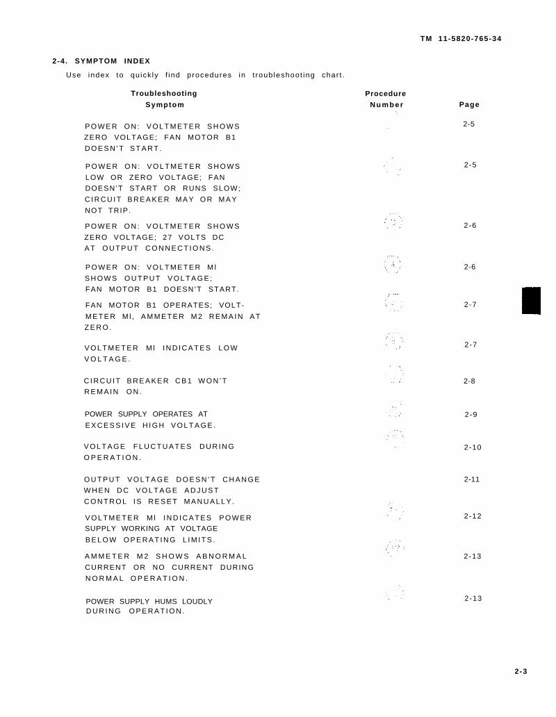
2-4. SYMPTOM INDEX
Use index to qu ick ly f ind procedures in t roub leshoot ing char t .
Troubleshooting
Symptom
P O W E R O N : V O L T M E T E R S H O W S
ZERO VOLTAGE; FAN MOTOR B1
D O E S N ’ T S T A R T .
P O W E R O N : V O L T M E T E R S H O W S
LOW OR ZERO VOLTAGE; FAN
DOESN’T START OR RUNS SLOW;
C I R C U I T B R E A K E R M A Y O R M A Y
NOT TRIP.
P O W E R O N : V O L T M E T E R S H O W S
ZERO VOLTAGE; 27 VOLTS DC
A T O U T P U T C O N N E C T I O N S .
P O W E R O N : V O L T M E T E R M l
S H O W S O U T P U T V O L T A G E ;
FAN MOTOR B1 DOESN’T START.
FAN MOTOR B1 OPERATES; VOLT-
M E T E R M l , A M M E T E R M 2 R E M A I N A T
Z E R O .
V O L T M E T E R M l I N D I C A T E S L O W
V O L T A G E .
C I R C U I T B R E A K E R C B 1 W O N ’ T
R E M A I N O N .
POWER SUPPLY OPERATES AT
E X C E S S I V E H I G H V O L T A G E .
V O L T A G E F L U C T U A T E S D U R I N G
O P E R A T I O N .
O U T P U T V O L T A G E D O E S N ’ T C H A N G E
W H E N D C V O L T A G E A D J U S T
C O N T R O L I S R E S E T M A N U A L L Y .
V O L T M E T E R M l I N D I C A T E S P O W E R
SUPPLY WORKING AT VOLTAGE
B E L O W O P E R A T I N G L I M I T S .
A M M E T E R M 2 S H O W S A B N O R M A L
CURRENT OR NO CURRENT DURING
N O R M A L O P E R A T I O N .
POWER SUPPLY HUMS LOUDLYD U R I N G O P E R A T I O N .
Procedure
N u m b e r Page
2-5
2-5
2-6
2-6
2-7
2-7
2-8
2-9
2-10
2-11
2-12
2-13
2-13
2-3

para 2-10
para 2-10
TM 11--5820-765-34
2 - 5 . T R O U B L E S H O O T I N G C H A R T
char t is des igned to supplement operat iona l checks in TM 11-5820-765-12.
Connect power supply to power source to conduct test procedures.to locate repa i r p rocedures in Sect ion I I I .
1 C o l o r c o o r d i n a t e d M A L F U N C T I O N / S Y M P T O M t o P R O B A B L E C A U S E z e r o e s i n o n t h e p r o -
blem area.
2 W A R N I N G S , C A U T I O N S a n d N O T E S a p p e a r w h e n a p p l i c a b l e .
3 F l o w s l o g i c a l l y , t a k i n g t e c h n i c i a n f r o m m o s t p r o b a b l e t o l e a s t l i k e l y c a u s e o f m a l f u n c t i o n .
4 I l l u s t r a t e d a i d s s p e e d p r o c e d u r e a n d i n c r e a s e a c c u r a c y .
2-4

para 2-10
para 2-10
T M 1 1 - 5 8 2 0 - 7 6 5 - 3 4
2-5
para 2-10
para 2-10
para 2-10
1 1 - 5 8 2 0 - 7 6 5 - 3 4
2 - 6

para 2-8
para 2-6
para 2-10
para 2-8
para 2-8
paragraph 2-8
paragraph 2-8
para 2-10
T M 1 1 - 5 8 2 0 - 7 6 5 - 3 4
2 - 7

para 2-10
T M 1 1 - 5 8 2 0 - 7 6 5 - 3 4
2 - 8

para 2-7
paragraph 2-7
para 2-8 paragraph 2-8
para 2-6
para 2-6
para 2-10
FO-2 FO-3
T M 1 1 - 5 8 2 0 - 7 6 5 - 3 4
2 - 9

paragraph 2-7
para 2-8 paragraph 2-8
para 2-6
paragraph 2-8
para 2-7
T M 1 1 - 5 8 2 0 - 7 6 5 - 3 4
2 - 1 0

para 2-7
paragraph 2-7
para 2-8 para 2-8
para 2-6
para 2-8
para 2-6
T M 1 1 - 5 8 2 0 - 7 6 5 - 3 4
2 - 1 1

paragraph 2-8
para 2-6
para 2-7
paragraph 2-7
para 2-8 paragraph 2-8
para 2-8
T M 1 1 - 5 8 2 0 - 7 6 5 - 3 4
2 - 1 2

T M 1 1 - 5 8 2 0 - 7 6 5 - 3 4
2-13

TM 11-5820-765-34
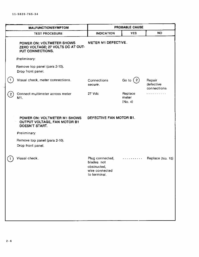
2-6. COMPONENT TESTING
The fo l lowing vo l tage and res is tance measurements show i f d iodes, meters , and cont ro l led rec-
t i f ie rs are defec t ive
CAPACITORS CARRY A CHARGE AFTER POWER SUPPLY IS SHUT OFF
B E F O R E P E R F O R M I N G T E S T S :
SHUT OFF POWER SUPPLY.
D I S C O N N E C T F R O M A C P O W E R S O U R C E .
DISCHARGE CAPACITORS BY SHORTING OUT WITH SHORTING ROD.
Diodes
T e s t e q u i p m e n t : M u l t i m e t e r T S - 3 5 2 B / U
Measure: In terna l res is tance, both d i rec t ions .
Mul t imeter se lec t swi tch : RX1
P r o c e d u r e :
Remove pane l (s ) .
D isconnect d iode be ing tes ted by remov ing screws and leads.
Connect mul t imeter leads to ends of d iode; take reading.
Reverse leads on d iode; take reading.
Diode defec t ive i f read ing shows:
Forward res is tance more than 5000 ohms.Reverse res is tance less than 500 ohms.
O ohms, both d i rec t ions .
Reconnect d iodes. Rep lace pane l (s ) .
Meter M1
F u n c t i o n :
50-vo l t , 1000-ohm-per-vo l t meter .
T e s t e q u i p m e n t :
M u l t i m e t e r T S - 3 5 2 B / U
V o l t m e t e r A N / U S M - 9 8 A
P r o c e d u r e :
Open f ront panel for both tests .
2-14

TM 11-5820-765-34
Defec t tes t :
Set mul t imeter to RX1000.
Connect leads across meter te rmina ls ; take read ing.
Mul t imeter should read 50,000 ohm res is tance across termina ls .
D i f f e r e n t r e a d i n g i n d i c a t e s d e f e c t .
A c c u r a c y t e s t :
Set mul t imeter to RX1.
P a r a l l e l - c o n n e c t V o l t m e t e r A N / U S M - 9 8 A a c r o s s m e t e r ’ s t e r m i n a l s .
Check zero-ad jus t - move zero-ad jus t screw in bo th d i rec t ions .
Needle on Ml sca le should be moveable above and be low zero l ine.
Meter M2
F u n c t i o n : 5 0 - m i l l i v o l t m e t e r
T e s t e q u i p m e n t : V o l t m e t e r A N / U S M - 9 8 A
A c c u r a c y t e s t :
P a r a l l e l - c o n n e c t v o l t m e t e r a c r o s s m e t e r t e r m i n a l s .
C h e c k z e r o - a d j u s t m o v e m e n t .
Needle on M2 sca le should be moveable above and be low zero l ine.
Controlled Rectifiers
T e s t e q u i p m e n t : M u l t i m e t e r T S - 3 5 2 B / U
M e a s u r e : I n t e r n a l r e s i s t a n c eSet mul t imeter to RX1.
P r o c e d u r e :
Remove pane l (s ) .
D isconnect gate and cathode leads o f rec t i f ie r be ing tes ted.
T e s t s :
A n o d e - c a t h o d e r e s i s t a n c e :
Connect mul t imeter leads to oppos i te s ides o f rec t i f ie r .
Rect i f ie r de fec t ive i f read ing shows: O ohms in both d i rec t ions .
1 megohm or h igher in both d i rect ions.
G a t e - c a t h o d e r e s i s t a n c e :
Reverse leads .
Rect i f ie r de fec t ive i f read ing shows 5000 ohms or h igher ( Ind ica tes open c i rcu i t ) .
N O T E
R e a d i n g f o r g a t e - c a t h o d e r e s i s t a n c e s h o u l d b e a p p r o x i m a t e l y 1 0 0 0 o h m s
( low res is tance sca le on ohmmeter ) .
R e c o n n e c t r e c t i f i e r l e a d s .
2 - 1 5
TM 11-5820-765-34
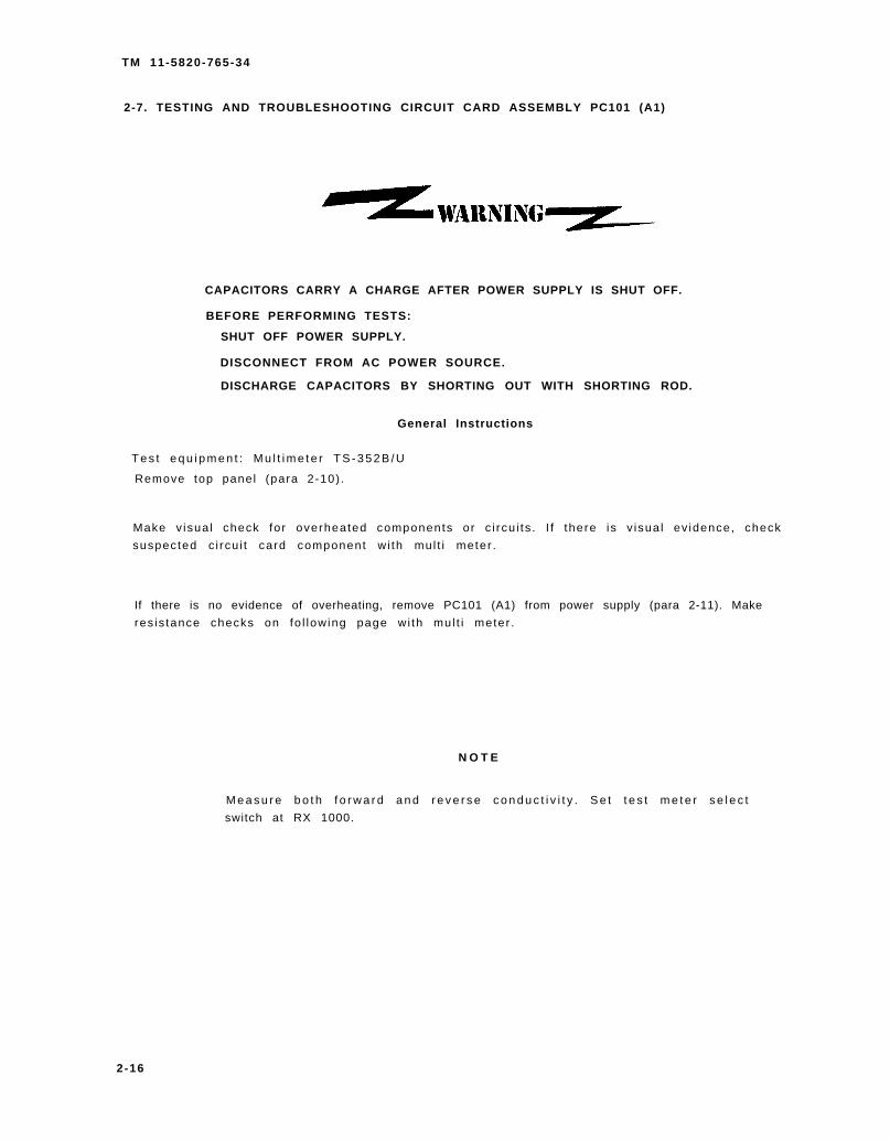
2-7. TESTING AND TROUBLESHOOTING CIRCUIT CARD ASSEMBLY PC101 (A1)
CAPACITORS CARRY A CHARGE AFTER POWER SUPPLY IS SHUT OFF.
BEFORE PERFORMING TESTS:
SHUT OFF POWER SUPPLY.
DISCONNECT FROM AC POWER SOURCE.
DISCHARGE CAPACITORS BY SHORTING OUT WITH SHORTING ROD.
General Instructions
T e s t e q u i p m e n t : M u l t i m e t e r T S - 3 5 2 B / U
Remove top panel (para 2-10) .
Make v isua l check fo r overheated components or c i rcu i ts . I f there is v isua l ev idence, check
suspected c i rcu i t card component w i th mul t i meter .
If there is no evidence of overheating, remove PC101 (A1) from power supply (para 2-11). Make
res is tance checks on fo l lowing page wi th mul t i meter .
N O T E
M e a s u r e b o t h f o r w a r d a n d r e v e r s e c o n d u c t i v i t y . S e t t e s t m e t e r s e l e c t
switch at RX 1000.
2-16

para 3-6
fig. 2
TM 11-5820-765-34
Checking PC101
M e a s u r e : R e s i s t a n c e o f a s s e m b l y c o m p o n e n t s .
C o n n e c t i o n : L o c a t i o n o f c o n n e c t o r t e r m i n a l s P C 1 0 1 :
( b o t t o m v i e w )
2 - 1 7

TM 11-5820-765-34
2-8. VOLTAGE AND RESISTANCE DATA
Open f ront , remove top panel (para 2-10) . Pu l l in ter lock swi tch up.
VOLTAGE OUTPUT, POWER TRANSFORMER T1
V o l t a g e m e a s u r e m e n t s , T 1 s e c o n d a r y w i n d i n g s , n o r m a l o p e r a t i n g c o n d i t i o n s :
Between secondary AC voltage indication (approximate)
winding terminals PP-4763 PP-4763A
TB4-1 T B 4 - 2 5 0 52.0
TB1-11 T B 1 - 1 0 115.0 115.0
T B 1 - 6 T B 1 - 7 3 2 3 3 . 4
T B 1 - 6 T B 1 - 8 6 4 6 6 . 7
DC RESISTANCE, TRANSFORMER and REACTORS
M e a s u r e r e s i s t a n c e w i t h p o w e r O F F .
D i s c o n n e c t p o w e r p l u g , t u r n s w i t c h O F F b e f o r e t a k i n g m e a s u r e m e n t s .
Remove top panel (para 2-10) .
C h e c k t r a n s f o r m e r , r e a c t o r s f o r d e f e c t s b e f o r e m a k i n g r e s i s t a n c e m e a s u r e m e n t s .
U s e t r o u b l e s h o o t i n g c h a r t .
C A U T I O NNormal res is tance measurements may not detec t some arc ing and shor t ing that occurs dur ing
normal operat ion. Use s ight , smel l , and hear ing to t ry to iso la te defect ive par t .
D C r e s i s t a n c e s : Convert readings to zero orchange test equipment
Transformer,reactors Between terminals Resistance (ohms) (*)
PP-4763 T1 T B 1 - 3 T B 1 - 1 2 0.06
TB4-1 T B 4 - 2 0 . 0 1 5
TB1-11 T B 1 - 1 0 2 . 6
T B 1 - 8 T B 1 - 6 0 . 4 0
T B 1 - 8 T B 1 - 7 0 . 4 0
N O T E
(*) For all readings below 1 ohm, table should read less than 1 ohm.
2 - 1 8
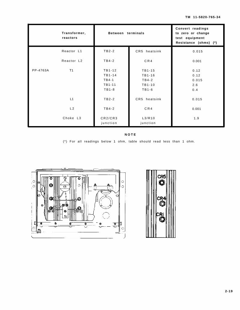
TM 11-5820-765-34
Transformer ,reactors
Reactor L1
R e a c t o r L 2
PP-4763A T1
L1
L 2
C h o k e L 3
Between terminals
T B 2 - 2
T B 4 - 2
T B 1 - 1 2
T B 1 - 1 4
TB4-1
TB1-11
T B 1 - 8
T B 2 - 2
T B 4 - 2
C R 2 / C R 3
j u n c t i o n
C R 5 h e a t s i n k
C R 4
T B 1 - 1 5
T B 1 - 1 6
T B 4 - 2
T B 1 - 1 0
T B 1 - 6
C R 5 h e a t s i n k
C R 4
L 3 / R 1 0
j u n c t i o n
Convert readingsto zero or change
test equipmentResistance (ohms) (*)
0 . 0 1 5
0.001
0 . 1 2
0 . 1 2
0 . 0 1 5
2.6
0 . 4
0 . 0 1 5
0.001
1.9
N O T E
( * ) For a l l read ings be low 1 ohm, tab le should read less than 1 ohm.
2-19
TM 11-5820-765-34
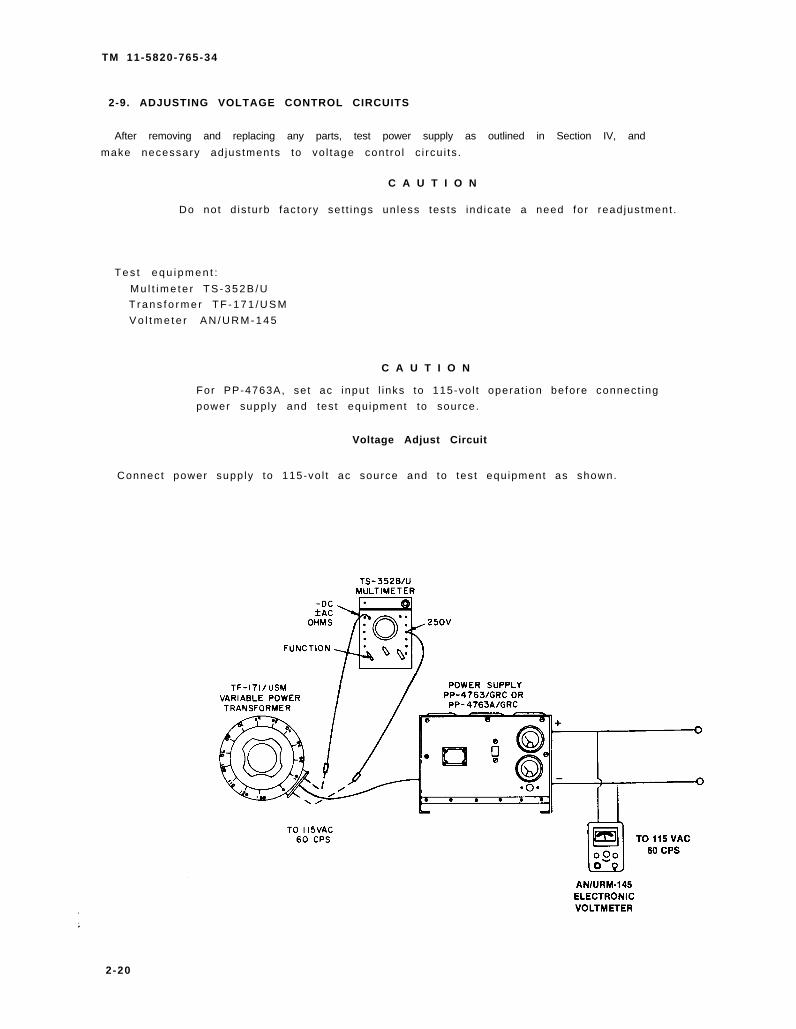
2-9. ADJUSTING VOLTAGE CONTROL CIRCUITS
After removing and replacing any parts, test power supply as outlined in Section IV, and
make necessary ad jus tments to vo l tage cont ro l c i rcu i ts .
C A U T I O N
Do not d is turb fac tory se t t ings un less tes ts ind ica te a need for read jus tment .
T e s t e q u i p m e n t :
M u l t i m e t e r T S - 3 5 2 B / U
T r a n s f o r m e r T F - 1 7 1 / U S M
V o l t m e t e r A N / U R M - 1 4 5
C A U T I O N
For PP-4763A, se t ac input l inks to 115-vo l t opera t ion before connect ing
power supply and test equ ipment to source.
Voltage Adjust Circuit
Connect power supp ly to 115-vo l t ac source and to tes t equ ipment as shown.
2-20

TM 11-5820-765-34
P r o c e d u r e :
Set transformer for 1 15-volt output.
Remove dc vo l tage-ad jus t pane l cover .
Open f ront panel .
Swi tch CB1: ON
Set dc vo l tage-ad jus t cont ro l R4 fu l l y c lockwise .
Loosen locknut on var iab le res is tor R8.Adjust R8 unt i l power supply vo l tage is 29 vo l ts min imum, 30 vo l ts max imum,
( take reading on Vol tmeter AN/URM-145) .
T i g h t e n l o c k n u t .
C B 1 : O F F
Close f ront paneI .
Overvoltage Circuit
Remove rear panel (refer to para 2-10).Connect jumper lead across s i l i con Cont ro l led Rect i f ie r SCRI (Q1) as shown. Use No. 8 (or
la rger ) AWG wi re .
Set t ransformer to 115-vo l t output .
Wi th no load connected across power supp ly ’s dc output :
Increase AC l ine vo l tage input to power supp ly unt i l dc output reads 35 vo l ts ±0.1 vo l t (on
Vol tmeter ME-30(* ) /U) , o r unt i l Cont ro l led Rect i f ie r SCR2(Q2) f i res , t r ipp ing CB1.
If SCR2(Q2) does not f ire:
Turn Var iab le Res is tor PC101R123(A1R23) c lockwise unt i l SCR2(Q2) f i res a t 35 vo l ts ±0.1 vo l t .
Refer to f igure 1, f igure 2, Chapter 3-6.
Sea l ad jus tment screw on PC101R123(A1R23) .
Remove a l l input power to supply .
Remove jumper leads f rom SCR1(Q1) .
Replace rear panel .
2-21

TM 11-5820-765-34
Sect ion I I I . MAINTENANCE PROCEDURES
S h u t o f f p o w e r s u p p l y b e f o r e p e r f o r m i n g m a i n t e n a n c e .
Capac i to rs car ry a charge a f te r power supp ly is shut o f f .
Shor t ou t capac i to rs w i th shor t ing rod.
Be carefu l dur ing removal and rep lacement .
Y o u c a n p r e v e n t a c c i d e n t a l d a m a g e t o o t h e r p a r t s , a n d y o u c a n p r e v e n t
potent ia l shor t c i rcu i ts caused by dropped hardware.
When removing and rep lac ing a par t , check carefu l ly for loose hardware or
i n s e c u r e e l e c t r i c a l c o n n e c t i o n s .
Do not operate equipment unt i l you make these checks.
N O T E
N o s p e c i a l t o o l s o r p r o c e d u r e s a r e n e e d e d t o r e m o v e a n d r e p l a c e p o w e r
s u p p l y p a r t s .
2-10. REMOVING AND REPLACING PANELS.
The power supp ly ’s f ront , top, and rear pane ls can be removed to a l low main tenance ins ide the
u n i t .
To rep lace top pane l , connect fan p lug and rep lace 15 screws, washers , nu ts .
2-22

TM 11-5820-765-34
Front Panel
Remove f ive machine screws, washers, nuts.
To rep lace f ron t pane l , rep lace screws, washers , nu ts .
Rear Panel
N O T E
Two people are requi red for removal and rep lacement .
Pos i t ion power supp ly to prov ide access to the bot tom.
Remove four screws, washers, nuts on the bottom (rear side) of the power supply.Return power supply to upr ight pos i t ion.
2 - 2 3

T M 1 1 - 5 8 2 0 - 7 6 5 - 3 4
Tag and remove the fo l lowing wi res f rom the rear panel :
PP-4763
W6 from SCR1.
W8 and W134 f rom TB3.
W56 f rom POS output terminal .
W 5 7 f r o m N E G o u t p u t t e r m i n a l .
W138 f rom TB2.
L1 and L2 f rom TB1.
POS and NEG f rom TB1.
2 - 2 4

TM 11-5820-765-34
PP-4763A
W6 from Q1 (heats ink).
W8 and W134 from TB3.
W12 and W13 from TB2.
W201 and W202 from FL1.
POS and NEG from FL1.
Remove rear panel .
To rep lace rear panel , so lder ident i f ied wi res to proper termina ls .
Position rear panel.
Replace six screws, washers, nuts on the side panels.
Replace four screws, washers, nuts on the bottom of the power supply.
2-25
para 2-10
TM 11-5820-765-34
2-11 . REMOVING AND REPLACING PARTS.
M a i n t e n a n c e p r o c e d u r e s a r e n u m b e r e d f o r e a s y a c c e s s . T r o u b l e s h o o t i n g p r o c e d u r e n u m b e r s
are g iven as a c ross- re ference.
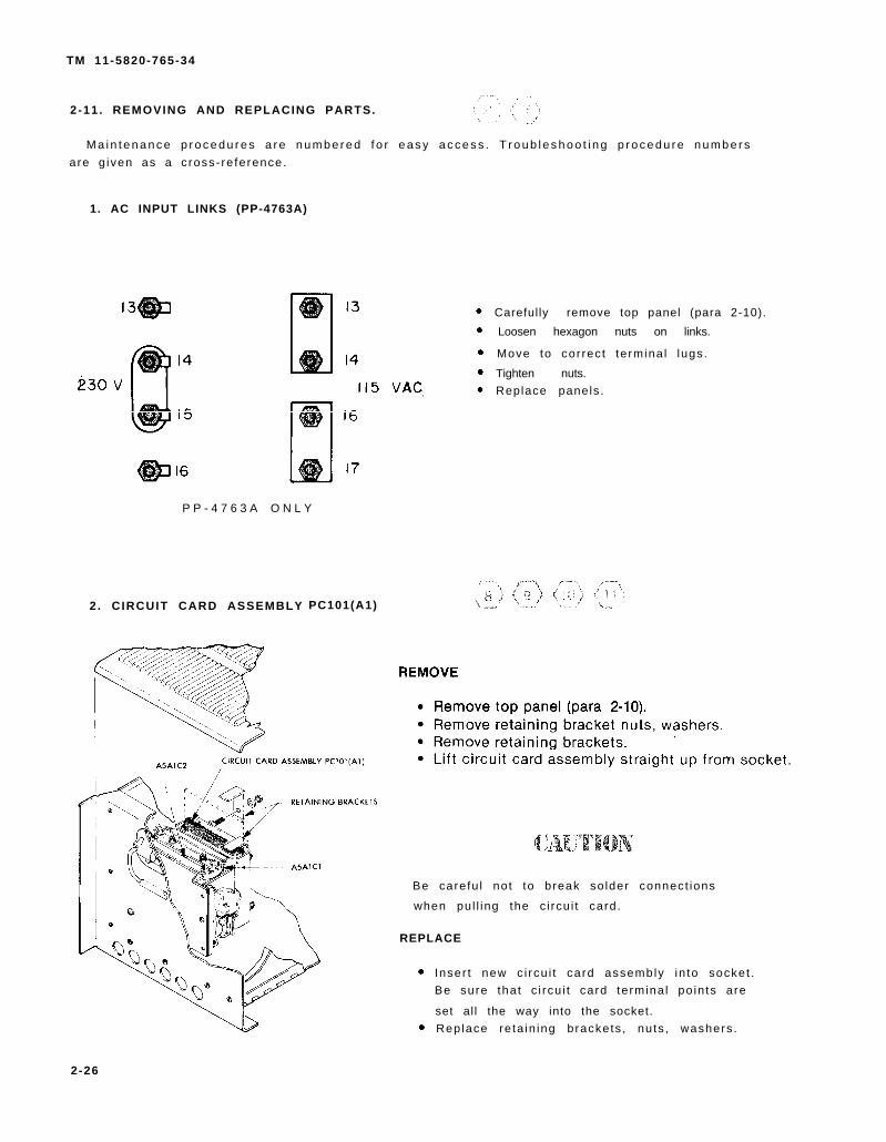
1. AC INPUT LINKS (PP-4763A)
Carefully remove top panel (para 2-10).
Loosen hexagon nuts on links.
Move to cor rec t te rmina l lugs .
Tighten nuts.
Replace panels.
P P - 4 7 6 3 A O N L Y
2. CIRCUIT CARD ASSEMBLY PC101(A1)
Be carefu l not to break so lder connect ions
when pul l ing the c i rcu i t card.
REPLACE
Inser t new c i rcu i t card assembly in to socket .
Be sure that c i rcu i t card te rmina l po in ts are
set al l the way into the socket.
Rep lace re ta in ing brackets , nu ts , washers .
2-26

TM 11-5820-765-34
3 . C I R C U I T B R E A K E R C B 1
REMOVE
Loosen two mach ine screws ( four screws, PP-4763A) .
Open f ront panel .
Remove screws, washers , nu ts .
Remove swi tch cover b racke t .
R e m o v e s w i t c h c o v e r .
D isconnect leads f rom c i rcu i t b reaker and tag .
Remove c i rcu i t b reaker .
2-27

TM 11-5820-765-34
4. VOLTMETER M1
REMOVE
Open f ront panel .
Remove th ree mach ine screws, washers , nu ts .
R e m o v e m e t e r m o u n t i n g g a s k e t .
Loosen termina l lugs, d isconnect leads (4763) ,u n s o l d e r c o n n e c t i o n s , a n d t a g .
R e m o v e m e t e r .
REPLACE
Insta l l new meter .
R e c o n n e c t l e a d s , t i g h t e n t e r m i n a l l u g s .
R e p l a c e m e t e r m o u n t i n g g a s k e t .
R e p l a c e m a c h i n e s c r e w s , w a s h e r s , n u t s .
2 - 2 8

TM 11-5820-765-34
5. AMMETER M2
REMOVE
Open front panel. Remove three machine screws, washers, nuts. Remove meter mounting gasket. Loosen terminal lugs, disconnect leads and tag. Remove meter.
REPLACE
Install new meter. Replace leads, tighten terminal lugs. Replace meter mounting gasket. Replace machine screws, washers, nuts.
2-29

TM 11-5820-765-34
6. DC VOLTAGE ADJUST COMPONENTS
RESISTOR R4
REMOVE
Open front panel.Remove two outside screws, nuts, washers.Unsolder leads, and tag.
Remove locknut, mounting nut, washer. Remove resistor.
REPLACE
RESISTOR R8
Put new resistor in place.Replace screw, nut, washer.Solder leads.Replace two outside screws, nuts, washers.
REMOVE
Open front panel.Remove two outside screws, nuts, washers.Unsolder leads and tag.Remove locknut, mounting nut, washer.Remove resistor.
REPLACE
Put new resistor in place.Replace screw, nut, washer.Solder leads.Replace two outside screws, nuts, washers.
2-30

TM 11-5820-765-34
RESISTOR R11
REMOVE
Open f ront panel .
Remove two outs ide screws, nu ts , washers .
Unsolder resistor lead.Remove nut , washer , w i re wrap, nut ,
w a s h e r s f r o m t e r m i n a l .
Cut w i re wrap around res is tor .
R e m o v e r e s i s t o r .
REPLACE
Put res is tor in p lace.Ins ta l l new wi re wrap around res is tor .
Rep lace nut , washer , w i re wrap,
nut , washer .So lder res is tor lead.
CAPACITORS C3 (PP-4763)
REMOVE
O p e n f r o n t p a n e l .
Remove res is tor R11 ( fo l low s teps above) .
Unsolder leads.
R e m o v e c a p a c i t o r .
REPLACE
Put new capac i to r in p lace.
S o l d e r l e a d s .
Rep lace res is tor R11 ( fo l low s teps above) .
2 - 3 1
TM 11-5820-765-34
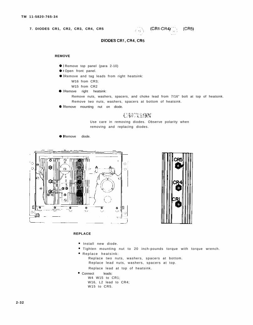
7. DIODES CR1, CR2, CR3, CR4, CR5
REMOVE
Remove top panel (para 2-10)
Open front panel.
Remove and tag leads from right heatsink:
W16 from CR3;
W15 from CR2
Remove right heatsink:
Remove nuts, washers, spacers, and choke lead from 7/16” bolt at top of heatsink.
Remove two nuts, washers, spacers at bottom of heatsink.
Remove mounting nut on diode.
Use care in removing diodes. Observe polarity when
removing and replacing diodes.
Remove diode.
REPLACE
Insta l l new diode.
T ighten mount ing nut to 20 inch-pounds torque wi th torque wrench.
R e p l a c e h e a t s i n k :Rep lace two nuts , washers , spacers a t bo t tom.Replace lead nuts , washers , spacers a t top .
Replace lead at top of heats ink.
Connect leads:W4 W15 to CR1;W16, L2 lead to CR4;W15 to CR5.
2-32

TM 11-5820-765-34
DIODES CR2, CR3
REMOVE
Remove top panel (para 2-10)
Open front panel.
Remove and tag leads from right heatsink:
W16 from CR3;
W15 from CR2
Remove right heatsink:
Remove nuts, washers, spacers, and choke lead from 7/16” bolt at top of heatsink.
Remove two nuts, washers, spacers at bottom of heatsink.
Remove mounting nut on diode.
Use care in removing diodes. Observe polarity when
removing and replacing diodes.
Remove diode.
REPLACE
Insta l l new diode.
T ighten mount ing nut to 20 inch-pounds torque wi th torque wrench.
R e p l a c e h e a t s i n k :
R e p l a c e t w o m a c h i n e s c r e w s a t b o t t o m .
Rep lace nuts , washers , spacers , and choke lead
on 7/16” bo l t a t top of heats ink.
C o n n e c t l e a d s :
W16 to CR3;
W15 to CR2.
2-33

TM 11-5820-765-34
8. REACTOR L2
REMOVERemove top panel (para 2-10) .
Open f ront panel .
D isconnect leads W17, W18.
Remove mount ing screw, washers on f ront , nu t on rear .
Remove bracket re ta in ing screw, nut , nu ts and washers .
Sl ide reactor s t ra ight out .
S l ide new reactor in to bracket .
Replace bracket re ta in ing screw, nut , nuts
a n d w a s h e r s .
Connect leads W17, W18.
Rep lace mount ing screw, washers , nu ts .
2 - 3 4

T M 1 1 - 5 8 2 0 - 7 6 5 - 3 4
9. CAPACITORS C1, C2
Capac i to rs car ry a charge a f te r power supp ly is shut o f f .
Shor t ou t capac i to rs w i th shor t ing rod.
REMOVE
Remove top panel.
Remove left side panel. Remove six machine
screws, three hex nuts.
Remove four screws on side panel.
Remove two screws from capacitor bank
a s s e m b l y s i d e p a n e l .
Remove two screws from + and - bus
bars o f de fec t ive capac i to r .
Slide capacitor out.
2-35

TM 11-5820-765-34
Make sure pos i t i ve mark ing (+) on capac i to r goes to the pos i t i ve mark ing
(+) on bus bar .
REPLACE
Sl ide new capac i to r in to assembly .
Replace two screws of capacitor bank assembly.
Replace power supp ly s ide pane l .
R e m o u n t c a p a c i t o r b a n k a s s e m b l y t o s i d e
panel with four screws.
2 - 3 6

TM 11-5820-765-34
10. RESISTOR R3
R E M O V E
Remove top panel (para 2-10).
Remove nuts , washers .
Tag and d isconnect leads.
Remove res is to r .
REPLACE
Ins ta l l new res is tor .C o n n e c t l e a d s .
Rep lace nuts , washers .
Replace top panel .
R E M O V E
Remove top panel (para 2-10) .
Unbol t rear panel .
D isconnect leads and tag:
W 6 f r o m d i o d e h e a t s i n k
W8 f rom TB3-2W134 from TB3-1
POS wi re f rom TB1 POS termina l
NEG wi re f rom TB1 NEG termina l
L1, L2 from TB1 terminal L2 (PP-4763)L l , L2 f rom TB1 terminal L2 (PP-4763A)
DC output termina l leads W136
from TB2-4.
R e m o v e m o u n t i n g n u t , w a s h e r .
R e m o v e d i o d e .
REPLACE
Apply thermal compound (Item No. 3
Appendix B) to mounting surface
of heatsink.
Ins ta l l new SCR.
Torque to 120 inch/pounds with
t o r q u e w r e n c h .
Connect gate lead of SCR to TB3.
Connect cathode lead of SCR to TB3.
2 - 3 7

TM 11-5820-765-34
12. DIODE SCR2 (Q2)
REMOVE
Remove top panel (para 2-10).
Remove W138 from TB2-3.
Remove W12 from TB1-19.
Remove W13 from TB1-18.
Remove TB2 by removing two mounting screws.
Remove cathode lead of SCR from TB2-1.
Remove gate lead of SCR from TB2-3.
Remove SCR mount ing nut , washer , and Iockwasher .
REPLACE
Apply thermal compound (Item No. 3
Appendix B) to mounting surface of heatsinks.
Ins ta l l new SCR wi th washer , Iockwasher , nu t .
Torque to 120 inch/pounds wi th torque wrench.
Connect cathode lead of SCR to TB2-1.
Connect gate lead of SCR to TB2-3.
Replace TB2 to rear pane l w i th two mount ing screws.
Connect W138 to TB2-3.
Connect W12 to TB1-19.
Connect W13 to TB1-18.
Rep lace top cover .
2-38

TM 11-5820-765-34
13. AC CABLE W3
REMOVE
Remove top panel (para 2-10) .
Remove rear panel .
R e m o v e c a b l e c o n n e c t o r :
R e m o v e m a c h i n e s c r e w s .
R e m o v e c o n n e c t o r c l a m p s .
Remove nuts , washers .D i s c o n n e c t t h r e e c a b l e c o n n e c t i o n s .
R e m o v e c a b l e .
REMOVE
REPLACE
I n s t a l l n e w c a b l e .
R e p l a c e c a b l e c o n n e c t i o n s .
R e p l a c e n u t s , w a s h e r s .
R e p l a c e c a b l e c o n n e c t o r c l a m p s .
R e p l a c e m a c h i n e s c r e w s .Replace rear panel .
Replace top panel .
R E P L A C E
R e m o v e s c r e w s .
R e m o v e c a b l e p l u g c l a m p .
Remove cover insu la tor .
D i s c o n n e c t l e a d s i n s i d e .
R e m o v e c a b l e p l u g .
Insta l l new cable p lug.
C o n n e c t l e a d s i n s i d e p l u g .
R e p l a c e c o v e r i n s u l a t o r .
R e p l a c e c a b l e p l u g c l a m p .
R e p l a c e s c r e w s .
N O T E
Make sure connect ions are cor rec t .
2 - 3 9

TM 11-5820-765-34
15. FAN MOTOR B1
REMOVE
Remove top panel (para 2-10) .
Remove chass is p la te f rom top pane l : remove
four mach ine screws, nu ts , washers .
R e m o v e f a n m o t o r a s s e m b l y f r o m c h a s s i s
p la te : remove four screws, nu ts washers .
REPLACE
Ins ta l l new fan motor assembly onto chass is
p la te : rep lace four mach ine screws, nuts ,
w a s h e r s .
Replace chass is p la te on panel : rep lace four
mach ine screws, washers , nu ts .
2-40

T M 1 1 - 5 8 2 0 - 7 6 5 - 3 4
16. TRANSFORMER T1
TRANSFORMER T1
R E M O V E
Remove top panel, rear panel; open front panel (para 2-10).
Disconnect leads W70 and W71 from terminals TB4-1 and TB4-2.
2 - 4 1

TM 11-5820-765-34
PP 4763
Remove nuts , washers , s tuds , and s tandof fs tha t secure TB1 to t rans former .
Remove a l l w i res f rom TB1 and tag.
Use ra tchet , 7 /16” socket and ex tens ion to remove four nuts f rom t ransformer f rame
a s s e m b l y
L i f t t ransformer over rear mount ing bracket and care fu l ly remove.
PP 4763A
Remove nuts , washers , s tuds , and s tandof fs tha t secure TB1 to t rans former .
Remove wires from TB1 at 12, 13, 14, 15, 16, 6, 7, 8, 10, 11, and tag.
Use ra tchet , 7 /16” socket and ex tens ion to remove four nuts f rom t ransformer f rame
a s s e m b l y .
L i f t t ransformer over rear mount ing bracket and care fu l ly remove.
R E P L A C E PP 4763
C a r e f u l l y i n s t a l l n e w t r a n s f o r m e r
Replace four nuts on t ransformer f rame assembly .
Replace a l l leads.
Reat tach TB1 to t ransformer :
Rep lace nuts , washers , s tuds , s tandof fs .
PP 4763A
C a r e f u l l y i n s t a l l n e w t r a n s f o r m e r .
Rep lace four nuts on t ransformer f rame assembly .
Replace leads on TB1 at 12, 13, 14, 15, 16, 6, 7, 8, 10, 11, and tag.
Reat tach TB1 to t ransformer :
Rep lace nuts , washers , s tuds , s tandof fs .
17. DIODE CR6
REMOVE
Remove top panel (para 2-10) .
Open f ront panel .
Unsolder and tag:
W54 from TB 4-1W53 from TB 4-2
R e m o v e d i o d e m o u n t i n g n u t .
L i f t d iode out f rom rear of terminal board.
2-42

para 2-10
TM 11-5820-765-34
N O T E
Ins ta l l d iode on rear o f terminal board on ly .
18. INTERLOCK SWITCH
R E M O V E
R E P L A C E
Install new diode.
Replace d iode mount ing nut .
Solder and tag:
W54 to TB 4-1
W53 to TB 4-2
R E P L A C E
Connect and tag two leads.
Replace two screws holding switch assembly.
Replace top panel .
2-43

Section IV
2-12
2-13
TM 11-5820-765-34
P e r f o r m t e s t s l i s t e d b e l o w a f t e r p e r f o r m i n g m a i n t e n a n c e o n e q u i p m e n t . T h e s e t e s t s d e t e r m i n e
i f equ ipment has been proper ly repai red and can be re turned to use. Repai red equipment must
meet per formance s tandards g iven on page 2-48.
Read ins t ruc t ions care fu l ly be fore us ing char t .
Per fo rm each s tep in sequence. DO NOT vary sequence.
Per form a l l requi red act ions.
Per form each tes t p rocedure .
Check each procedure aga ins t i t s per formance s tandard .
Tools , tes t equipment , and mater ia ls : re fer to page 2-1.
General
Disconnect power supply from power source ond other equipment.
T e s t e q u i p m e n t a n d m a t e r i a l s : N o n e r e q u i r e d .
T e s t c o n n e c t i o n s a n d c o n d i t i o n s : N o c o n n e c t i o n s n e c e s s a r y .
Procedures
Cont ro l se t t ings : AC power swi tch may be in any pos i t ion .
L e g e n d : T e s t P r o c e d u r e s
P e r f o r m a n c e S t a n d a r d
Test Chart
(1) Check case for damage, miss ing par ts , cond i t ion o f pa in t :
No damage to case, no par ts miss ing.
Sur faces needing pa in t do not show bare meta l .
Panel le t ter ing readable.
(2) Remove top panel (para 2-10):
Check chass is fo r damage, miss ing par ts .
No damage or miss ing par ts .
Check mechan ica l assembl ies fo r loose or miss ing screws, bo l ts , nu ts .
Screws, bo l ts , nu ts are t igh t . None miss ing .
Check a l l e lec t r ica l assembl ies fo r loose or miss ing par ts .
Par ts are t igh t . None miss ing.
(3) Opera te power swi tch :
O p e r a t e s p r o p e r l y .
(4) Turn motor B1 fan b lades:
B lades tu rn f ree ly w i thout s t ick ing .
2 - 4 4
TM 11-5820-765-34
(5 ) Check ac cab le assembly :
Insulat ion not f rayed or damaged.
(6) Check ac cable W3P1 (PP-4763A):
P lug secure ly a t tached to cab le , not damaged.
(7 ) Res is tance check o f in te r lock swi tch S1:
O p e r a t e s p r o p e r l y ( r e f e r t o
S1 open reading is O ohms.
S1 c losed read ing is 2 .2K.
Replace top panel .
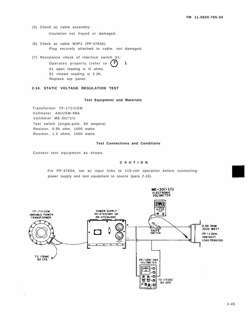
2-14. STATIC VOLTAGE REGULATION TEST
Test Equipment and Materials
T r a n s f o r m e r T F - 1 7 1 / U S M
V o l t m e t e r A N / U S M - 9 8 A
V o l t m e t e r M E - 3 0 ( * ) / U
Test swi tch (s ing le-po le , 60 ampere)
Resis tor , 0 .56 ohm, 1000 wat ts
Resis tor , 1 .3 ohms, 1000 wat ts
Test Connections and Conditions
C o n n e c t t e s t e q u i p m e n t a s s h o w n .
C A U T I O N
For PP-4763A, se t ac input l inks to 115-vo l t opera t ion before connect ing
power supply and test equipment to source (para 2-10).
2-45

TM 11-5820-765-34
T E S T E Q U I P M E N T S E T T I N G S :
T r a n s f o r m e r
M u l t i m e t e r
Contro l : 115 vo l ts
FUNCTION swi tch : AC VOLTS, 250 VOLT SCALE
Black test lead: OHMS – DC + AC jack
Red test lead: 2.5 jack, 1000 OHMS PER VOLT
A C D C c o l u m n
V o l t m e t e r A N / U S M - 9 8 A Range: 50 volt
N u l l : V T V M
V o l t m e t e r M E - 3 0 ( * ) / U Swi tch: 0 .3 vo l ts (ca l ibra ted)
L o a d 0.56 ohm, 1000-wat t res is tor
T e s t s w i t c h O p e n
N O T E
Keep test equ ipment a t these set t ings except where noted.
(1) Equipment set as noted above.
1 C h e c k a c c u r a c y o f v o l t m e t e r M l ; c o m p a r e
A N / U S M - 9 8 A r e a d i n g s .
2 C l o s e t e s t s w i t c h . C h e c k r i p p l e v o l t a g e
on ME-30(* ) /U.
3 C h e c k d c o u t p u t v o l t a g e o n A N / U S M - 9 8 A .
(2) Transformer : 127 vo l ts .
T e s t s w i t c h c l o s e d .
Check dc vo l tage output on AN/USM-98A.
(3) Load: 1 .3 ohm, 1000-wat t res is tor .
T e s t s w i t c h c l o s e d .
Check dc output vo l tage.
C i rcu i t b reaker CB1 ON.
Set dc vo l tage ad just R4 for 28-vo l t output .
Less than 1.0 vo l t d i f ference between readings.
Vol tage wi th in 1% rms (approx imate ly 3% peak
to peak) of output vo l tage.
Reading wi th in +0.5% of 28 vo l ts dc (max imum
vol tage dev ia t ion 280 mi l l i vo l ts or less) .
DC voltage: 28 volts.
Reading wi th in +0.5% of 28 vo l ts dc (280 mV or
less dev ia t ion) .
DC vo l tage ad jus t : 28 vo l ts .
Reading wi th in +0.5% of 28 vo l ts dc (280 mV or
less dev ia t ion) .
2 - 4 6

TM 11-5820-765-34
TEST EQUIPMENT
TEST PROCEDURE
(4 ) Transformer : 103 vo l ts .
Load: 1 .3-ohm res is tor .
T e s t s w i t c h c l o s e d .
Check dc output vo l tage.
(5) Transformer : 127 vo l ts .
Load: 1 .3-ohm res is tor .
T e s t s w i t c h c l o s e d .
Check dc output vo l tage.
(6) Tes t swi tch open.
Load reduced to zero.
Check dc output vo l tage.
(7) Transformer : 103 vo l ts .
T e s t s w i t c h o p e n .
Load reduced to zero.
Check dc output vo l tage.
(8) Transformer : 127 vo l ts .T e s t s w i t c h o p e n .
Load reduced to zero.
Check dc output vo l tage.
(9) Load: 1 .3-ohm res is tor .T e s t s w i t c h c l o s e d .
Check dc output vo l tage.
(10) Load: 1 .3-ohm res is tor .
T e s t s w i t c h c l o s e d .
Check dc output vo l tage.
EQUIPMENT UNDER TEST
PERFORMANCE STANDARD
DC vol tage: 28 vo l ts
Reading wi th in +0.5% of 28 vo l ts dc (280 mV or
less dev ia t ion) .
DC vo l tage: 28 vo l ts
Reading wi th in +0.5% of 28 vo l ts dc (280 mV or
less dev ia t ion) .
DC vo l tage: 28 vo l ts
Reading wi th in +0.5 % of 28 vo l ts dc (280 mV or
less dev ia t ion) .
DC vo l tage: 28 vo l ts
Reading wi th in +0.5 % of 28 vo l ts dc (280 mV or
less dev ia t ion) .
DC vo l tage: 28 vo l ts
Reading wi th in +0.5 ’% of 28 vo l ts dc (280 mV or
less dev ia t ion) .
DC vo l tage: Set for min imum vo l tage
(full Cw).
Reading between 22 and 27 vo l ts dc.
DC vo l tage: Set fo r max imum vo l tage ( fu l l C W) .
Reading between 29 and 30 vo l ts dc.
RESET DC VOLTAGE ADJUST FOR 28-VOLT OUTPUT ± 0 .1 VOLT
C I R C U I T B R E A K E R : O F F
TURN OFF POWER TO ALL TEST EQUIPMENT.
2-47

TM 11-5820-765-34
Verifying PP-4763A 230-volt input
The above vo l tage regu la t ion tes t was conducted a t 115 vo l ts . I f a 230-vo l t , s ing le-phase, 50/60
Hz power source is available, test PP-4763A at 230-volt input.
P r o c e d u r e :
Set TB-1 ac input l inks to 230 volts ac.
Connect power cab le to 230-vo l t source.
Repeat test equipment settings, control settings for step 1 of paragraph 2-14 in test chart.
Repeat ripple voltage, dc output voltage checks in step 1 of paragraph 2-14.
2-15. TEST DATA SUMMARY
S u m m a r y o f p e r f o r m a n c e s t a n d a r d s .
Input
V o l t a g e 115 vol ts
115 or 230 volts
F r e q u e n c y 50/60 Hz
P h a s e S i n g l e
C u r r e n t
( fu l l load) 2 3 a m p e r e s
23 amperes at 115-vol t input
11.5 amperes at 230-vol t input
Output
V o l t a g e 28-volt operation (27-29 volts dc)
Current ( fu l l load) 5 0 a m p e r e s
R i p p l e V o l t a g e 1.0 percent rms
( m a x i m u m )
PP-4763
PP-4763A
PP-4763
PP-4763A
V o l t a g e R e g u l a t i o n
S t a t i c v o l t a g e : * 0 . 5 p e r c e n t ( m a x i m u m t o t a l v o l t a g e
deviat ion 280 mi l l ivo l ts) .
2-48

TM 11-5820-765-34
CHAPTER 3
G E N E R A L S U P P O R T M A I N T E N A N C E
Sect ion I . GENERAL INFORMATION
P A G E
General . . . . . . . . . . . . . . . . . . . . . . . . . . . . . . . . . . . . . . . . . . . . . . . . . . . . . . . . . . . . . . . . . . . . . . 3-2
Repair Parts, Tools, Test Equipment, and Materials . . . . . . . . . . . . . . . . . . . . . . . . . . . . . . . . . . 3-2
Sect ion I I . TROUBLESHOOTING
Procedures . . . . . . . . . . . . . . . . . . . . . . . . . . . . . . . . . . . . . . . . . . . . . . . . . . . . . . . . . . . . . . . . . . . 3-3
Testing and Troubleshooting Circuit Card Assembly PC101(A1) . . . . . . . . . . . . . . . . . . . . . . . 3-3
Section III . MAINTENANCE PROCEDURES
Removing and Replacing Circuit Card Assembly PC101(A1) . . . . . . . . . . . . . . . . . . . . . . . . . . . 3-6
Repairing Circuit Card Assembly PC101(A1) . . . . . . . . . . . . . . . . . . . . . . . . . .
Section IV. TEST PROCEDURES
. . . . . . . . . . . . . . 3 -6
Dynamic Voltage Regulation Test . . . . . . . . . . . . . . . . . . . . . . . . . . . . . . . . . . . . . . . . . . . . . . 3-10
Procedures . . . . . . . . . . . . . . . . . . . . . . . . . . . . . . . . . . . . . . . . . . . . . . . . . . . . . . . . . . . . . . . . . . . 3-10
Test DataSummary . . . . . . . . . . . . . . . . . . . . . . . . . . . . . . . . . . . . . . . . . . . . . . . . . . . . . . . . . . . . 3-13
3-1

TM 11-5820-765-34
Sect ion I . GENERAL INFORMATION
3-1. GENERAL
Low vo l tage, h igh amperage cur rent is present a t output connect ions and
c o n n e c t i o n s i n s i d e e q u i p m e n t .
S h u t o f f p o w e r s u p p l y b e f o r e p e r f o r m i n g m a i n t e n a n c e .
Be care fu l when work ing wi th 115 or 230-vo l t ac l ine connect ions.
Ser ious in ju ry or death may resu l t f rom contac t w i th te rmina ls .
T h i s c h a p t e r c o v e r s g e n e r a l s u p p o r t t r o u b l e s h o o t i n g , m a i n t e n a n c e , a n d t e s t i n g p r o c e d u r e s f o rthe power supp ly . Sect ion I l i s ts the too ls , tes t equ ipment , and mater ia ls needed to per form
genera l suppor t main tenance. Troubleshoot ing procedures are descr ibed in Sect ion I I ,
main tenance procedures in Sect ion I I I , and tes t procedures in Sect ion IV.
N O T E
T h i s c h a p t e r i s c o n f i n e d t o m a i n t e n a n c e o f c i r c u i t c a r d a s s e m b l yPC101(A1) . For a l l o ther main tenance ins t ruc t ions, see Chapter 2 .
3-2. REPAIR PARTS, TOOLS, TEST EQUIPMENT, AND MATERIALS
Repair Parts: Refer to TM 11-5820-765-34P-1.
Spec ia l Tools : No spec ia l too ls are needed.
Tools , Test Equipment , and Mater ia ls :
Item National Stock Number
TOOLS
T o o l K i t , E l e c t r o n i c E q u i p m e n t T K - 1 0 0 / G
T o o l K i t , E l e c t r o n i c E q u i p m e n t T K - 1 0 5 / G
T o r q u e W r e n c h , 1 5 0 i n c h - p o u n d s
TEST EQUIPMENT
M u l t i m e t e r T S - 3 5 2 B / U
O h m m e t e r Z M - 2 1 A / U
O s c i l l o s c o p e A N / U S M - 2 8 1 A
Transformer , Var iab le Power TF-171/USM
V o l t m e t e r , E l e c t r o n i c A N / U S M - 9 8 A
V o l t m e t e r , E l e c t r o n i c M E - 3 0 ( * ) / U
5180-00-605-0079
5180-00-610-8177
5120-00-230-6380
6625-00-553-0142
6625-00-643-1030
6625-00-228-2201
6120-00-503-0632
6625-00-753-2115
6625-00-643-1670
3-2

TM 11-5820-765-34
M A T E R I A L S
Resis tor , 0 .56 ohm, 1000 wat ts
Resis tor , 1 .3 ohms, 1000 wat ts
Test Swi tch , S ing le-Po le , 60 ampere
Wire, E lect r ica l , St randed; No. 8 AWG
Section II. TROUBLESHOOTING
5905-00-064-4679
3-3 . PROCEDURES
Fol low procedures in Chapter 2 to loca l ize and iso la te t roub le . Use paragraph 3-4 to tes t and
t r o u b l e s h o o t t h e c i r c u i t c a r d a s s e m b l y .
3-4. TESTING AND TROUBLESHOOTING CIRCUIT CARD ASSEMBLY PC101(A1).
Capac i to rs car ry a charge a f te r power supp ly is shut o f f .
B e f o r e p e r f o r m i n g t e s t s :
S h u t o f f p o w e r s u p p l y .
D i s c o n n e c t f r o m a c p o w e r s o u r c e .
D ischarge capac i to rs by shor t ing out w i th shor t ing rod.
General Instructions
Remove top panel (para 3-5).
Make v isua l check fo r overheated components or c i rcu i ts . I f there is v isua l ev idence, check
s u s p e c t e d c i r c u i t c a r d c o m p o n e n t w i t h m u l t i m e t e r .
If there is no evidence of overheating, remove circuit card from the unit (para 3-5) and ex-
amine i t . I f the board is b l is tered, c racked, or broken, the board must be rep laced. You can
rep lace defec t ive components and repa i r c racked or open-c i rcu i ted w i r ing .
Resistance Measurements
T e s t e q u i p m e n t : M u l t i m e t e r T S - 3 5 2 B / U
3-3

T M 1 1 - 5 8 2 0 - 7 6 5 - 3 4
Checking PC101
M e a s u r e : R e s i s t a n c e o f a s s e m b l y c o m p o n e n t s .
C o n n e c t i o n : L o c a t i o n o f c o n n e c t o r t e r m i n a l s P C 1 0 1 :
P C 1 0 1 J 1 0 1 B e t w e e n t e r m i n a l s Forward resistance Reverse resistance
.
12-30 1 0 K Higher (greater than 20K)
12-26 1 0 K Higher (greater than 20K)
4-6 1 K - 4 K 1 K - 4 K
12-34 1 1 K I n f i n i t y
26-30 4 5 K 4 5 K
6-12 Z e r o Z e r o
6-36 High (greater than 10K) High (greater than 10K)
6-38 High (greater than 10K) High (greater than 10K)
10-22 High (greater than 10K) High (greater than 10K)
10-12 1 4 K 2 0 0 K
Checking A1 (PP-4763-A)
M e a s u r e : R e s i s t a n c e o f a s s e m b l y c o m p o n e n t s .
Test po in ts : A1TP1 through A1TP6.
C o n n e c t i o n s : L o c a t i o n o f t e s t p o i n t s :
Make same res is tance measurements as above ( re fer to f ig . 2 , para 3-6) .
Make d i rec t res is tance measurements o f A1 components , us ing these tes t po in ts :
A1 Test Points Between A1J101 Terminals
A 1 T P 3
A 1 T P 2
A 1 T P 5
A1TP1 to A1TP2
A 1 T P 6
A 1 T P 4
3 4
12
1 2
1 2
6
Forward Resistance Reverse Resistance
4 0 0 K I n f i n i t y
5 0 K I n f i n i t y
0 l 0 0 K
2.1 K 2 . 5 K
3-4

TM 11-5820-765-34
Voltage and Osci l loscope Measurements, A1 (PP-4763A)
T e s t e q u i p m e n t : O s c i l l o s c o p e A N / U R M - 1 4 0 A
V o l t m e t e r , E l e c t r o n i c M E - 3 0 ( * ) / U
Measure : Charac ter is t i c vo l tages, wave shapes.
N O T E
Use extender board; i f none available, modify a test lead for voltage or wave
s h a p e .
A1 TEST POINTS BETWEEN VOLTAGE OR WAVE SHAPE
T B 1 - 8 A 1 T P 5 20 volts dc
A 1 T P 2 T B 1 - 8 20 vol ts dc
A 1 T P 6 T B 1 - 8 9 volts dc
T B 2 - 4 A 1 T P 6 9 volts dc
A1 TEST POINTS BETWEEN VOLTAGE OR WAVE SHAPE
3-5

TM 11-5820-765-34
Section III . MAINTENANCE PROCEDURES
3-5. REMOVING AND REPLACING CIRCUIT CARD ASSEMBLY PC101(A1)
REMOVE
Remove top panel:Remove 15 machine screws, nuts, washers.
D i s c o n n e c t f a n m o t o r p l u g .
Remove re ta in ing bracket nu ts , washers .
Remove re ta in ing brackets .
L i f t c i rcu i t card assembly s t ra igh t up f rom socket .
C A U T I O N
Be carefu l not to break so lder connect ions
when pul l ing the c i rcu i t card.
REPLACE
Inser t c i rcu i t card in to socket .
Be sure that the c i rcu i t card termina l po in ts are
set a l l the way in to the socket .Rep lace re ta in ing brackets , nu ts , washers .
3 - 6 . REPAIRING CIRCUIT CARD ASSEMBLY PC101(A1) (figs. 1 and 2)
Removing Protective Coating
Adequate ventilation should be provided while using TRICHLOROTRIFLUOROETHANE. Pro-
longed breathing of vapor should be avoided. The solvent should not be used near heat oropen flame; the products of decomposition are toxic and irritating. Since TRICHLOROTRI-
FLUOROETHANE dissolves natural oils, prolonged contact with skin should be avoided.When necessary, use gloves which the solvent cannot penetrate. If the solvent is taken
internally, consult a physician immediately.
C A U T I O N
Before s tar t ing repa i rs , remove pro tec t ive coat ing EC1103 f rom the c i rcu i t card assembly :
Isolate the area to be repaired.
If this area is small, scrape off the protective coating with a knife or other sharp tool.
I f th is a rea is la rge , soak the c i rcu i t card in TRICHLOROTRIFLUOROETHANE to so f ten
the coat ing, then wipe the area c lean wi th a l in t - f ree c lo th .
3-6
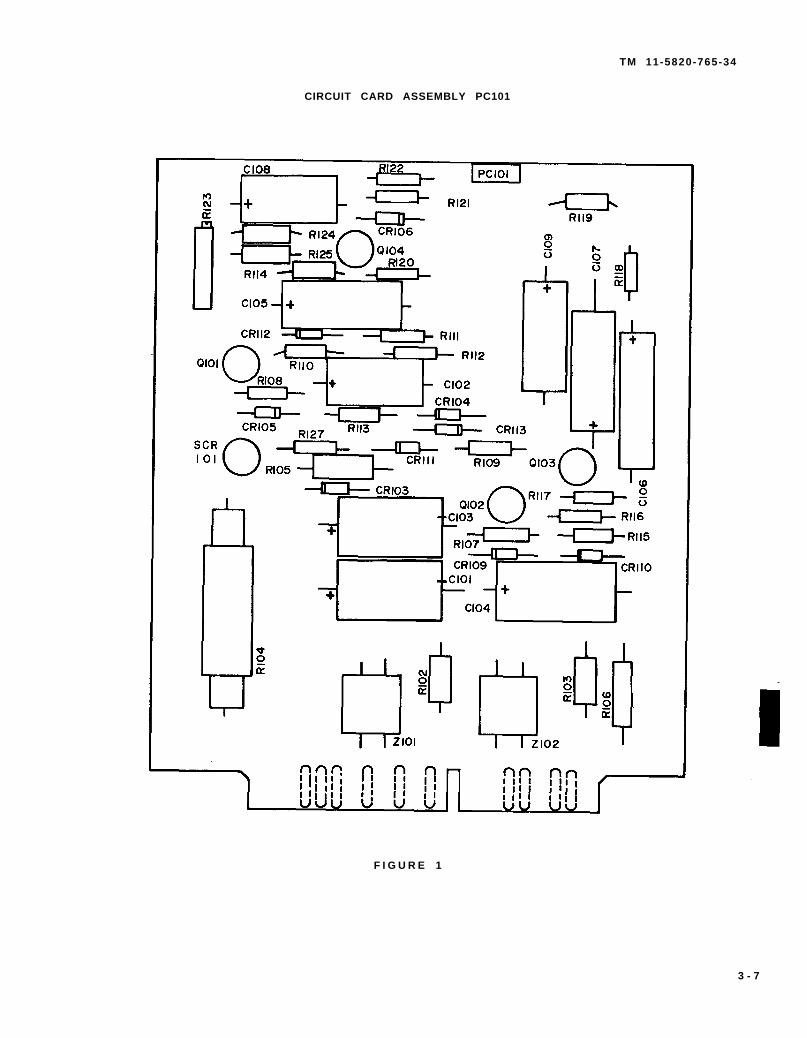
TM 11-5820-765-34
CIRCUIT CARD ASSEMBLY PC101
F I G U R E 1
3 - 7
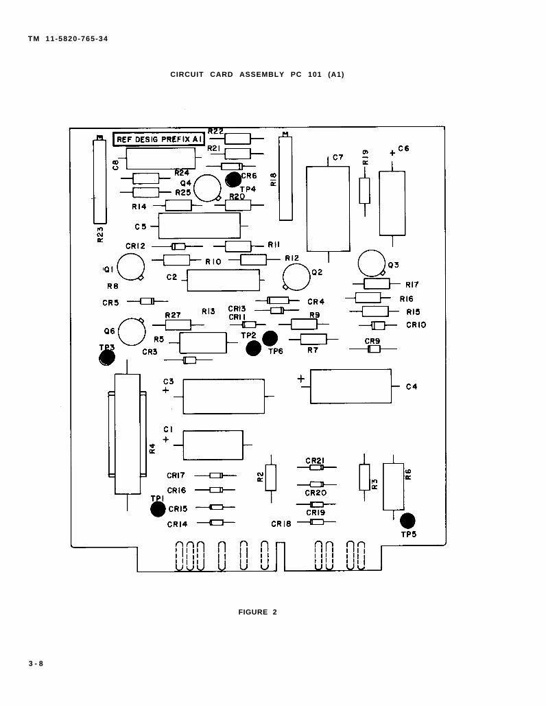
TM 11-5820-765-34
CIRCUIT CARD ASSEMBLY PC 101 (A1)
FIGURE 2
3 - 8

TM 11-5820-765-34
Repairing Printed Circuit Wiring
Use only a pencil-type soldering iron with a maximum rating of 25 watts.Excessive heat will cause printed wiring conductors to separate from theboard. For additional soldering techniques, refer to TB SIG 222.
Repair printed circuit wiring that has a crack, pinhole, cut, or notch more than 30 percent of thewire’s width.
Procedure:
Remove protective coating.Place a short length of flat bus wire over the defective wiring and hold it firmly in place.Solder the entire length of bus wire to the wiring.
Do not apply heat longer than needed. Prolonged heat can separate the con-ductor from the card; this damage cannot be repaired.
Apply protective coating to exposed area after completing repairs.
Replacing Defective Parts
Remove defective part:Cut leads on part between part and circuit card mounting holes.Cut leads as close to mounting holes as possible.
Remove protective coating around the part on the card’s printed wiring side.Heat printed wiring at mounting holes with soldering iron until solder melts.
Remove excess solder and remaining pieces of wire leads.
Do not apply heat longer than needed. Prolonged heat can separate theprinted wiring from the card, which will damage the care.
Bend the leads of replacement part to fit mounting holes.Insert leads in mounting holes from parts side of card; press part firmly against card.On card’s wiring side, cut leads of part; leave approximately 1/8 inch of leads protrudingfrom card.Bend and press these leads against printed circuit conductorUsing a heat sink, solder replacement part leads to printed circuit conductor.Apply protective coating to repaired area.
3-9

TM 11-5820-765-34
A f t e r c o m p l e t i n g
Applying protective Coating
repa i rs , app ly pro tec t ive coat ing to a l l exposed areas on c i rcu i t card .
Pro tec t ive coat ing EC1103 is tox ic .
The work area must be wel l vent i la ted.
A v o i d b r e a t h i n g t h e f u m e s .
I f the coat ing comes in contac t w i th sk in , immedia te ly wash the
sk in w i th soap and water .
Use a rubber eraser to clean areas to be coated.
Prepare the pro tec t ive coat ing mix ture :
Mix 70 parts protective coating (Item No. 2, Appendix B) with 30 parts naphtha (parts
by volume) (Item No. 4, Appendix B). Stir mixture thoroughly.
App ly coat ing mix ture to card by spray ing, d ipp ing, or brush ing.
When brush ing, be carefu l to prevent bubbles f rom forming.
Set coated card aside; al low it to dry in fresh air for f ive hours.
Section IV. TEST PROCEDURES
3-7 . PROCEDURES
Af ter per forming main tenance on c i rcu i t card assembly , per form s ta t ic vo l tage regu la t ion tes t
(para 2-14) and dynamic vo l tage regula t ion tes t be low. Repai red equipment must meet per-formance s tandards g iven on page 3-11.
3-8. DYNAMIC VOLTAGE REGULATION TEST
Test Equipment and Materials
M u l t i m e t e r T S - 3 5 2 B / U
O s c i l l o s c o p e A N / U S M - 2 8 1 A
T r a n s f o r m e r T F - 1 7 1 / U S M
V o l t m e t e r A N / U S M - 9 8 A
V o l t m e t e r M E - 3 0 ( * ) / U
Resis tor , 0 .56 ohm, 1000-wat t
T e s t s w i t c h , s i n g l e - p o l e , 6 0 a m p e r e
3-10

TM 11-5820-765-34
C o n n e c t t e s t e q u i p m e n t a s
Test Connections and Conditions
s h o w n .
C A U T I O N
For PP-4763A, se t ac input l inks to 115 vo l t opera t ion before connect ing
power supply and test equ ipment to source.
T E S T L E G E N D
TEST EQUiPMENT EQUIPMENT UNDER TEST
TEST PROCEDURE PERFORMANCE STANDARD
T E S T E Q U I P M E N T S E T T I N G S :
T r a n s f o r m e r
M u l t i m e t e r
V o l t m e t e r A N / U S M - 9 8 A
Contro l : 115 vo l ts
FUNCTION swi tch : AC VOLTS, 250 VOLT SCALE
Black tes t lead: OHMS -DC ±AC jack
Red test lead: 2.5 jack, 1000 OHMS PER VOLT
A C - D C c o l u m n
Range: 50 vol t
N u l l : V T V M
Polar i ty : Set so 50 VOLTS meter ind icator
def lec ts to r igh t dur ing tes t .
L o a d
T e s t s w i t c h
0.56 ohm, 1000-wat t res is tor
O p e n
3-11

TM 11-5820-765-34
T E S T L E G E N D
TEST EQUIPMENT
TEST PROCEDURE
EQUIPMENT UNDER TEST
PERFORMANCE STANDARD
N O T E
Keep test equ ipment a t these set t ings except where noted.
1. Equipment set as noted above. Power ON.
DC vo l tage ad jus t R4; 28-vo l t ou tput .
2 . C lose tes t sw i tch . Trans ient vo l tage less than 5 vo l ts .
C h e c k d y n a m i c r e s p o n s e o n
o s c i l l o s c o p e . R e s p o n s e t i m e s :
PP-4763: Recovery to within 1.85 volts of f inal
va lue less than 50 mi l l i seconds.
PP-4763A: Recovery to w i th in 37 percent o f f ina l
va lue less than 75 mi l l i seconds.
3 . Open tes t sw i tch .
C h e c k d y n a m i c r e s p o n s e o n
o s c i l l o s c o p e .
4 . P o w e r O F F .
C h e c k d y n a m i c r e s p o n s e o n
o s c i l l o s c o p e .
5 . Power ON.
C h e c k d y n a m i c r e s p o n s e o n
o s c i l l o s c o p e .
Trans ient vo l tage less than 5 vo l ts .
R e s p o n s e t i m e s :
PP-4763: Recovery to within 1.85 volts of f inal
va lue less than 100 mi l l i seconds.
PP-4763A: Recovery to w i th in 37 percent o f f ina l
vo l tage less than 125 mi l l i seconds.
DC vo l tage overshoot less than 5 vo l ts .
DC vo l tage overshoot less than 5 vo l ts .
Power OFF. Turn off power to all test equipment.
3-12

TM 11-5820-765-34
3-9. TEST DATA SUMMARY
S u m m a r y o f p e r f o r m a n c e s t a n d a r d s .
V o l t a g e
F r e q u e n c y
P h a s e
C u r r e n t
( fu l l load)
Input
115 vol ts
115 or 230 volts
50/60 Hz
S i n g l e
2 3 a m p e r e s
23 amperes at 115-vol t input
11.5 amperes at 230-vol t input
PP-4763
P P - 4 7 6 3 A
PP-4763
P P - 4 7 6 3 A
V o l t a g e 2 8 - v o l t o p e r a t i o n
Current ( fu l l load) 5 0 a m p e r e s
R i p p l e V o l t a g e 1.0 percent rms
( m a x i m u m )
Output
(27-29 volts dc)
V o l t a g e R e g u l a t i o n
Stat ic : ±0.5 percent (maximum to ta l vo l tage dev ia t ion 280 mi l l i vo l ts )
Dynamic voltage regulation
PP-4763 Response time (milliseconds) Recovery Value
PP-4763A
Ful l load
L o a d O F F7 5
1 2 5
W i t h i n 1 3 7 p e r c e n t
o f f ina l va lue
3 - 1 3 / ( 3 - 1 4 / B L A N K )

TM 11-5820-765-34
APPENDIX A
REFERENCES
A - 1 . I N T R O D U C T I O N
Fol lowing is a l i s t o f a l l fo rms, techn ica l bu l le t ins , and techn ica l manuals re ferenced in th is
m a n u a l .
A - 2 . F O R M S
Quality Deficiency Report . . . . . . . . . . . . . . . . . . . . . . . . . . . . . . . . . . . . . . . . .. SF 368
Recommended Changes to Equipment Technical Manuals . . . . . . . . . . . . . . DA Form 2028-2
Recommended Changes to Publications and Blank Form . . . . . . . . . . . . . . . . DA Form 2028
A-3. TECHNICAL BULLETINS
Solder and Soldering . . . . . . . . . . . . . . . . . . . . . . . . . . . . . . . . . . . . . . . . . . . . . . . . . . . .. TB SIG 222
Safety Precautions for Maintenance of Electrical/Electronic Equipment . . . . . TB 385-4
A-4. TECHNICAL MANUALS
Direc t Supor t and Genera l Suppor t Main tenance Repai r Par ts and Spec ia l
Too ls L is ts ( Inc lud ing Depot Main tenance Repai r Par ts and Spec ia l
Too ls ) fo r Power Supp l ies PP-4763/GRC (NSN 5820-00-937-7690) and
PP-4763A/GRC(NSN 5820-00-13768), . . . . . . . . . . . . . . . . . . . . . . . . . . . . . . TM 11-5820-765-34P-1
O p e r a t o r ’ s a n d O r g a n i z a t i o n a l M a i n t e n a n c e M a n u a l : P o w e r S u p p l i e s ,
PP-4763/GRC (NSN 5820-00-937-7690) and PP-4763A/GRC (NSN
5820-00-113-9768) . . . . . . . . . . . . . . . . . . . . . . . . . . . . . . . . . . . . . . . . . . . . . . TM 11-5820-765-12
Operator ’s Manual : Rad io Sets AN/GRC-106 (NSN 5820-00-402-2263) and
AN/GRC-106A(NSN 5820-00-223-7548) . . . . . . . . . . . . . . . . . . . . . . . . . . . . . TM 11-5820-520-10
Procedures fo r Dest ruc t ion o f E lec t ron ics Mater ie l to Prevent Enemy Use
(Electronics Command) . . . . . . . . . . . . . . . . . . . . . . . . . . . . . . . . . . . . . . . . . TM 750-244-2
The Army Maintenance Management System (TAMMS) . . . . . . . . . . . . . . . . TM 38-750
A-1/A-2 blank
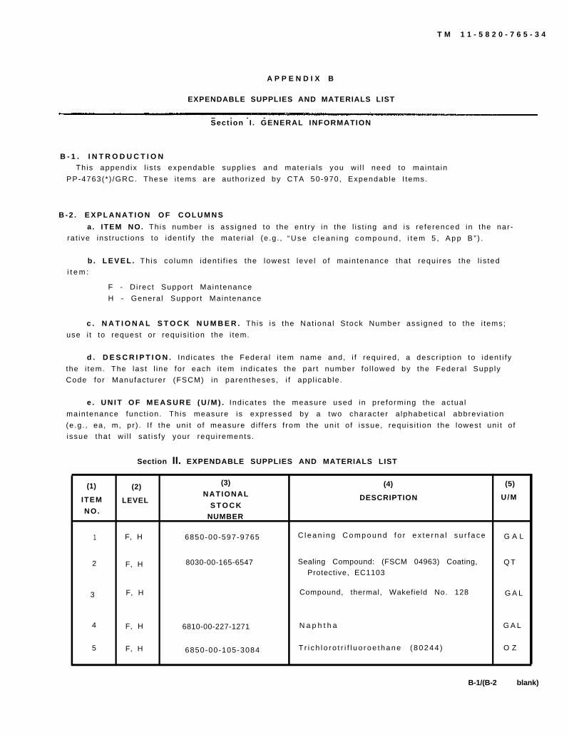
T M 1 1 - 5 8 2 0 - 7 6 5 - 3 4
A P P E N D I X B
EXPENDABLE SUPPLIES AND MATERIALS LIST
Sect ion I . GENERAL INFORMATION
B - 1 . I N T R O D U C T I O NThis appendix l i s ts expendable supp l ies and mater ia ls you wi l l need to main ta in
PP-4763(* ) /GRC. These i tems are author ized by CTA 50-970, Expendable I tems.
B - 2 . E X P L A N A T I O N O F C O L U M N S
a. ITEM NO. This number is ass igned to the ent ry in the l is t ing and is re ferenced in the nar -
ra t ive ins t ruct ions to ident i fy the mater ia l (e .g . , “ U s e c l e a n i n g c o m p o u n d , i t e m 5 , A p p B ” ) .
b . L E V E L . This co lumn ident i f ies the lowest leve l o f main tenance that requ i res the l i s ted
i t e m :
F - D i rec t Suppor t Main tenance
H - Genera l Suppor t Main tenance
c . N A T I O N A L S T O C K N U M B E R . This is the Nat iona l S tock Number ass igned to the i tems;
use i t to request or requis i t ion the i tem.
d . D E S C R I P T I O N . Ind icates the Federa l i tem name and, i f requ i red, a descr ip t ion to ident i fy
the i tem. The las t l ine for each i tem ind icates the par t number fo l lowed by the Federa l Supply
Code for Manufacturer (FSCM) in parentheses, i f app l icab le .
e . U N I T O F M E A S U R E ( U / M ) . Ind icates the measure used in pre forming the ac tua l
main tenance funct ion . Th is measure is expressed by a two character a lphabet ica l abbrev ia t ion
(e.g . , ea, m, pr ) . I f the un i t o f measure d i f fers f rom the un i t o f issue, requ is i t ion the lowest un i t o f
issue tha t w i l l sa t is fy your requ i rements .
Section II. EXPENDABLE SUPPLIES AND MATERIALS LIST
(1) (2) (3) (4) (5)
ITEM LEVELNATIONAL
S T O C KDESCRIPTION U/M
NO.NUMBER
1 F, H 6850-00-597-9765 C l e a n i n g C o m p o u n d f o r e x t e r n a l s u r f a c e G A L
2 F, H 8030-00-165-6547 Sealing Compound: (FSCM 04963) Coating, Q TProtective, EC1103
3 F, H Compound, thermal, Wakefield No. 128 G A L
4 F, H 6810-00-227-1271 N a p h t h a G A L
5 F, H 6850-00-105-3084 T r i c h l o r o t r i f l u o r o e t h a n e ( 8 0 2 4 4 ) O Z
B-1/(B-2 blank)
TM 11-5820-765-34
I N D E X
S U B J E C TA
P A G E
AC cable W3 . . . . . . . . . . . . . . . . . . . . . . . . . . . . . . . . . . . . . . . . . . . . . . . . . . . . . . . . . . . . . . . 2-39
AC cable plug W3P1 (PP 4763A). . . . . . . . . . . . . . . . . . . . . . . . . . . . . . . . . . . . . . . . . . . . . . . 2-39
AC input links (PP 4763A) . . . . . . . . . . . . . . . . . . . . . . . . . . . . . . . . . . . . . . . . . . . . . . . . . . . . 2-26
Adjusting voltage control circuits . . . . . . . . . . . . . . . . . . . . . . . . . . . . . . . . . . . . . . . . . . . . . 2-20
Ammeter M2 . . . . . . . . . . . . . . . . . . . . . . . . . . . . . . . . . . . . . . . . . . . . . . . . . . . . . . . . . . . . . . . 2-29
B
Block diagram analysis . . . . . . . . . . . . . . . . . . . . . . . . . . . . . . . . . . . . . . . . . . . . . . . . . . . . . . 1-5
C
Capacitor C1, C2 . . . . . . . . . . . . . . . . . . . . . . . . . . . . . . . . . . . . . . . . . . . . . . . . . . . . . . . . . . . . 2-35
Chart, troubleshooting . . . . . . . . . . . . . . . . . . . . . . . . . . . . . . . . . . . . . . . . . . . . . . . . . . . ...2-3
Circuit breaker CB1 . . . . . . . . . . . . . . . . . . . . . . . . . . . . . . . . . . . . . . . . . . . . . . . . . . . . . . . . . 2-27
Circuit card assembly PC 101(A1) . . . . . . . . . . . . . . . . . . . . . . . . . . . . . . . . . . . . . . . . . . . . . . 2-26
Circuits, control . . . . . . . . . . . . . . . . . . . . . . . . . . . . . . . . . . . . . . . . . . . . . . . . . . . . . . . . . . . . 1-8
Circuits, power and voltage . . . . . . . . . . . . . . . . . . . . . . . . . . . . . . . . . . . . . . . . . . . . . . . . . . . 1-6
Component testing . . . . . . . . . . . . . . . . . . . . . . . . . . . . . . . . . . . . . . . . . . . . . . . . . . . . . . ...2-14
Control circuits . . . . . . . . . . . . . . . . . . . . . . . . . . . . . . . . . . . . . . . . . . . . . . . . . . . . . . . . . . . . . 1-8
D
DC voltage adjust components . . . . . . . . . . . . . . . . . . . . . . . . . . . . . . . . . . . . . . . . . . . . . . . . 2-30
Description and data, equipment . . . . . . . . . . . . . . . . . . . . . . . . . . . . . . . . . . . . . . . . . . . . . . 1-2
Destruction ofarmymaterielto prevent enemy use . . . . . . . . . . . . . . . . . . . . . . . . . . . . ...1-2
Diagram analysis, block . . . . . . . . . . . . . . . . . . . . . . . . . . . . . . . . . . . . . . . . . . . . . . . . . . . . . . 1-5
Differences between models. . . . . . . . . . . . . . . . . . . . . . . . . . . . . . . . . . . . . . . . . . . . . . . . . 1-3
Diodes CRl, CR2,CR3,CR4,CR5. . . . . . . . . . . . . . . . . . . . . . . . . . . . . . . . . . . . . . . . . . . . . . 2-32
Diode CR6 . . . . . . . . . . . . . . . . . . . . . . . . . . . . . . . . . . . . . . . . . . . . . . . . . . . . . . . . . . . . . . . . . 2-43
Diode SCR1 (Q1) . . . . . . . . . . . . . . . . . . . . . . . . . . . . . . . . . . . . . . . . . . . . . . . . . . . . . . . . . . . . 2-37
Diode SCR2 (Q2) . . . . . . . . . . . . . . . . . . . . . . . . . . . . . . . . . . . . . . . . . . . . . . . . . . . . . . . . . . . . 2-38
E
Equipmentdescription anddata. . . . . . . . . . . . . . . . . . . . . . . . . . . . . . . . . . . . . . . . . . . . . . . 1-2
Equipment, purposeand use.. . . . . . . . . . . . . . . . . . . . . . . . . . . . . . . . . . . . . . . . . . . . . . . . 1-2
F
Fan motor Be . . . . . . . . . . . . . . . . . . . . . . . . . . . . . . . . . . . . . . . . . . . . . . . . . . . . . . . . . . ..2-40
I
Interlock switch . . . . . . . . . . . . . . . . . . . . . . . . . . . . . . . . . . . . . . . . . . . . . . . . . . . . . . . . . . . . 2-43
I n d e x - 1

TM 11-5820-765-34
INDEX - cont inued
S U B J E C TM
P A G E
Maintenance forms, records, and reports . . . . . . . . . . . . . . . . . . . . . . . . . . . . . . . . . . . . . . . 1-2
Maintenance procedures, direct support . . . . . . . . . . . . . . . . . . . . . . . . . . . . . . . . . . . . ...2-22
Removing and replacing panels . . . . . . . . . . . . . . . . . . . . . . . . . . . . . . . . . . . . . . . . . . . . . 2-22
Removing and replacing parts. . . . . . . . . . . . . . . . . . . . . . . . . . . . . . . . . . . . . . . . . . . . . . 2-26
Maintenance procedures, general support . . . . . . . . . . . . . . . . . . . . . . . . . . . . . . . . . . . . . . 3-6
Removing and replacing circuitcard assembly PC 101(A1) . . . . . . . . . . . . . . . . . . . . . . 3-6
Repairing circuit card assembly. . . . . . . . . . . . . . . . . . . . . . . . . . . . . . . . . . . . . . . . . . . . . 3-6
Materials, repair parts,tools,test equipment . . . . . . . . . . . . . . . . . . . . . . . . . . . . . . . . . . . . 2-1,3-2
Models, differences between.. . . . . . . . . . . . . . . . . . . . . . . . . . . . . . . . . . . . . . . . . . . . . . . . 1-3
P
Panels, removing and replacing . . . . . . . . . . . . . . . . . . . . . . . . . . . . . . . . . . . . . . . . . . . . ...2-22
Parts, removing and replacing. . . . . . . . . . . . . . . . . . . . . . . . . . . . . . . . . . . . . . . . . . . . . ...2-26
Physical tests and inspections. . . . . . . . . . . . . . . . . . . . . . . . . . . . . . . . . . . . . . . . . . . . . . . . 2-44
Powerand voltage circuits . . . . . . . . . . . . . . . . . . . . . . . . . . . . . . . . . . . . . . . . . . . . . . . . . . . 1-6
Procedures,troubleshooting,(direct support maintenance) . . . . . . . . . . . . . . . . . . . . . . . . 2-2
Procedures, troubleshooting, (general support maintenance) . . . . . . . . . . . . . . . . . . . . . . 3-3
Procedures, test . . . . . . . . . . . . . . . . . . . . . . . . . . . . . . . . . . . . . . . . . . . . . . . . . . . . . . . . . . . . 2-44, 3-10
Principles of operation, technical . . . . . . . . . . . . . . . . . . . . . . . . . . . . . . . . . . . . . . . . . . ...1-5
R
Reactor L2 . . . . . . . . . . . . . . . . . . . . . . . . . . . . . . . . . . . . . . . . . . . . . . . . . . . . . . . . . . . . . . . . . 2-34
Removing and repairingcircuitcard assembly PC 101(A1) . . . . . . . . . . . . . . . . . . . . . . . . . 3-6
Removing and replacing panels. . . . . . . . . . . . . . . . . . . . . . . . . . . . . . . . . . . . . . . . . . . . . . . 2-22
Removing and replacing parts. . . . . . . . . . . . . . . . . . . . . . . . . . . . . . . . . . . . . . . . . . . . . . . . 2-26
Repair parts, tools, testequipment and materials,(direct support) . . . . . . . . . . . . . . . . . . 2-1
Repair parts, tools, testequipment and materials, (general support). . . . . . . . . . . . . . . . . 3-2
Repairing circuit card assembly PC 101(A1) . . . . . . . . . . . . . . . . . . . . . . . . . . . . . . . . . . . . . 3-6
Reporting Equipment Improvement Recommendations (EIR) . . . . . . . . . . . . . . . . . . . . . 1-2
Resistor R3 . . . . . . . . . . . . . . . . . . . . . . . . . . . . . . . . . . . . . . . . . . . . . . . . . . . . . . . . . . . . . . . . 2-37
S
Safety, care, and handling . . . . . . . . . . . . . . . . . . . . . . . . . . . . . . . . . . . . . . . . . . . . . . . . . . . . 1-4
Static voltage regulation test . . . . . . . . . . . . . . . . . . . . . . . . . . . . . . . . . . . . . . . . . . . . . . . . . 2-45
Symptom index . . . . . . . . . . . . . . . . . . . . . . . . . . . . . . . . . . . . . . . . . . . . . . . . . . . . . . . . . . . . . 2-3
I n d e x - 2

TM 11-5820-765-34
INDEX - cont inued
S U B J E C TT
P A G E
Technical principles of operation. . . . . . . . . . . . . . . . . . . . . . . . . . . . . . . . . . . . . . . . . . . . . .
Test data summary, (direct support) . . . . . . . . . . . . . . . . . . . . . . . . . . . . . . . . . . . . . . . . . . . .
Test datasummary,(general support) . . . . . . . . . . . . . . . . . . . . . . . . . . . . . . . . . . . . . . . . . .
Test Legend, (direct support) . . . . . . . . . . . . . . . . . . . . . . . . . . . . . . . . . . . . . . . . . . . . . . . . .
Test Legend, (generaisupport). . . . . . . . . . . . . . . . . . . . . . . . . . . . . . . . . . . . . . . . . . . . . . . .
Test procedures,(direct support). . . . . . . . . . . . . . . . . . . . . . . . . . . . . . . . . . . . . . . . . . . . . .
Test procedures, (general support) . . . . . . . . . . . . . . . . . . . . . . . . . . . . . . . . . . . . . . . . . . . .
Testing, components . . . . . . . . . . . . . . . . . . . . . . . . . . . . . . . . . . . . . . . . . . . . . . . . . . . . . . . .
Testing and troubleshooting circuit card assembly . . . . . . . . . . . . . . . . . . . . . . . . . . . . . . .
Troubleshooting,(direct support maintenance) . . . . . . . . . . . . . . . . . . . . . . . . . . . . . . . . . .
Troubleshooting,(general support maintenance). . . . . . . . . . . . . . . . . . . . . . . . . . . . . . . . .
Troubleshooting chart . . . . . . . . . . . . . . . . . . . . . . . . . . . . . . . . . . . . . . . . . . . . . . . . . . . . . . .
Tools, repairparts, testequipment, materials . . . . . . . . . . . . . . . . . . . . . . . . . . . . . . . . . . . .
Transformer T1 . . . . . . . . . . . . . . . . . . . . . . . . . . . . . . . . . . . . . . . . . . . . . . . . . . . . . . . . . . . . .
V
1-5
2-48
3-13
2-46
3-11
2-44
3-10
2-14
2-16
2-2
3-3
2-3
2-1, 3-2
2-41
Voltage and power circuits . . . . . . . . . . . . . . . . . . . . . . . . . . . . . . . . . . . . . . . . . . . . . . . . . . . 1-6
Voltage and resistance data . . . . . . . . . . . . . . . . . . . . . . . . . . . . . . . . . . . . . . . . . . . . . . . . . . 2-18
Voltage control circuits,adjusting . . . . . . . . . . . . . . . . . . . . . . . . . . . . . . . . . . . . . . . . . . . . . 2-20
VoltmeterMl . . . . . . . . . . . . . . . . . . . . . . . . . . . . . . . . . . . . . . . . . . . . . . . . . . . . . . . . . . . ...2-28
Index-3

Figure FO-3
Figure FO-3
Figure FO-2
Figure FO-2
Figure FO-1
Figure FO-1
Figure FO-1
TM 11-5820-765-34
F O L D O U T I N D E X
C o l o r C o d e M a r k i n g f o r M i l i t a r y S t a n d a r d ( s h e e t 1 o f 2 ) .
C o l o r C o d e M a r k i n g f o r M i l i t a r y S t a n d a r d ( s h e e t 2 o f 2 ) .
P o w e r S u p p l y P P - 4 7 6 3 / G R C ( s h e e t 1 o f 2 ) .
P o w e r S u p p l y P P - 4 7 6 3 / G R C ( s h e e t 2 o f 2 ) .
P o w e r S u p p l y P P - 4 7 6 3 A / G R C ( s h e e t 1 o f 2 ) .
P o w e r S u p p l y P P - 4 7 6 3 A / G R C ( s h e e t 2 o f 2 ) .
ALL THE ABOVE L ISTED FOLDOUTS ARE LOCATED IN THE BACK OF THE MANUAL.
F.O. Index-1

Table 2
Table 1
Figure FO-1
TM 11-5820-765-34

GROUP I
GROUP II
GROUP III
Figure FO-1
TABLE III
TABLE I
TM 11-5820-765-34
TABLE II

TM 11-5820-765-34
Figure FO-2

Figure FO-2
TM 11-5820-765-34
TM 11-5820-765-34

Figure FO-3

Figure FO-3
TM 11-5820-765-34

By Order of the Secretary of the Army:
Official:
JOHN A. WICKHAM JR.General, United States Army
Chief of S ta f f
ROBERT M. JOYCEMajor General, United States Army
The Adjutant General
DISTR IBUT ION:
To be distributed in accordance with DA Form 12-51, Direct and General Support Maintenance re-quirements for PP-4763/GRC.


THE METRIC SYSTEM AND EQUIVALENTS

PIN: 053566-000

This fine document...
Was brought to you by me:
Liberated Manuals -- free army and government manuals
Why do I do it? I am tired of sleazy CD-ROM sellers, who take publicly available information, slap “watermarks” and other junk on it, and sell it. Those masters of search engine manipulation make sure that their sites that sell free information, come up first in search engines. They did not create it... They did not even scan it... Why should they get your money? Why are not letting you give those free manuals to your friends?
I am setting this document FREE. This document was made by the US Government and is NOT protected by Copyright. Feel free to share, republish, sell and so on.
I am not asking you for donations, fees or handouts. If you can, please provide a link to liberatedmanuals.com, so that free manuals come up first in search engines:
<A HREF=http://www.liberatedmanuals.com/>Free Military and Government Manuals</A>
– SincerelyIgor Chudovhttp://igor.chudov.com/
– Chicago Machinery Movers