title: low frequency 1/f noise of p-mos. bipolar, and · 2013-05-21 · low frequency 1/f noise of...
TRANSCRIPT

AN ABSTRACT OF THE THESIS OF
Mark Cheng for the degree of Master of Science in Electrical and Computer Engineering
presented on July 18. 2000.
Title: LOW FREQUENCY 1/f NOISE OF p-MOS. BIPOLAR, AND
LATERAL BIPOLAR TRANSISTORS
Abstract approved:
F
This thesis deals with 1/f noise in p-MOS, bipolar, and lateral bipolar transistors.
Experimental measurements determine the appropriate 1/f noise for MOSFET's, bipolar
transistors and lateral bipolar transistors.
The literature on 1/f noise in p-MOSFETs, bipolar transistors and lateral
bipolar transistors is reviewed. The two main sources of low frequency 1/f noise are
mobility fluctuations and number fluctuations. Our 1/f noise measurements in p-
MOSFET's, bipolar transistors, and lateral pnp bipolar transistors were done at
frequencies of 1 Hz and 1 KHz respectively by both the automatic and analog
methods. The measurement results suggest that the number fluctuation and mobility
fluctuation models are applied for short channel and long channel p-MOSFET's in
the saturation region respectively. Simulations have been done using PSPICE, with
Redacted for Privacy

noise level NLEV = 0 and device model level 3 for long channel p-MOSFET's; with
noise level NLEV = 2 and device model level 6 for short channel p-MOSFET's.
Theoretical considerations as well as experimental results show that it is possible to
take advantage of MOSFET and bipolar devices for low noise integrated circuit
applications. Research on low frequency 1/f noise in the different semiconductor
devices is very important to determine the best semiconductor structure and best noise
model for different devices. This is an especially important consideration in the
development of the integrated circuits in high-density chip area, low voltage supply,
low power consumption and low noise applications.

Copyright by Mark ChengJuly 18, 2000
All Rights Reserved

LOW FREQUENCY 1/f NOISE OF p-MOS, BIPOLAR AND LATERAL
BIPOLAR TRANSISTORS
by
Mark Cheng
A THESIS
submitted to
Oregon State University
in partial fulfillment of
the requirement for the degree of
Master of Science
Presented July 18, 2000
Commencement June, 2001
Master of Science thesis of Mark Cheng presented on July 18. 2000
APPROVED:
/
Major Professor, Engineering
Head of
Dean of
and Computer Engineering
I understand that my thesis will become part of the permanent collection of OregonState University libraries. My signature below authorizes release of my thesis to anyreader upon request.
Redacted for Privacy
Redacted for Privacy
Redacted for Privacy
Redacted for Privacy

ACKNOWLEDGEMENTS
I wish to express my special thanks and gratitude to Professor Leonard
Forbes for guiding my efforts in the right direction and providing a supporting
atmosphere for ideas to develop.
I also wish to express my great appreciation to Professor Un-Ku Moon and
Tenca Alexandre for providing the best available knowledge of analog and digital
circuit analysis and design which is relative to this project.
Thanks also to my group members, Dingming Xie, Zhunlin Zhou for their
helpful comments and cooperation.
And finally, I would like to thank the National Science Foundation Center
for the Design of Analog/Digital Integrated Circuits (CDADIC) for the generous
financial support.
This thesis is dedicated to my dearest wife, Xiaohai, for her constant
encouragement and support.

TABLE OF CONTENTS
1. Introduction
1.1 Low Frequency 1/f Noise in p-MOSFETs .1
1.2 Low Frequency 1/f Noise in PNP Bipolar Transistors ...........................3
1.3 Low Frequency 1/f Noise in Lateral PNP Bipolar Transistors .................. 5
2. Low Frequency 1/f Noise in p-MOSFETs............................................... 6
2.1 Measurement Principles .............................................................. 6
2.2 p-MOSFET 1/f Noise PSPICE Simulation ........................................ 9
2.3 Results and Discussions.............................................................. 9
3. Low Frequency 1/f Noise in Bipolar PNP Transistors................................ 18
3.1 Measurement Principles ............................................................. 18
3.2 Low Frequency 1/f Noise Models-Current Dependent Component ........... 18
3.3 Low Frequency 1/f Noise Models-Voltage Dependent Component...........27
3.4 Conclusion ............................................................................ 32
4. Low Frequency 1/f Noise in Lateral PNP Transistors ................................33
4.1 Measurement Principles.............................................................. 33
4.2 DC Characteristics of Lateral PNP Transistors.................................... 33
4.3 Results and Discussions.............................................................. 38
5. Conclusions .................................................................................44
BIBLIOGRAPHY ..........................................................................46
TABLE OF CONTENTS (Continued)
APPENDICES .51
Appendix A MATLAB Program .52Appendix B PSPICE Simulation Program for flicker noise .......................54Appendix C The sources of the PMOS and bipolar transistors ................... 56

LIST OF FIGURES
Figure pg1.1 Noise sources in bipolar transistors ...................................................... 4
2.1 Block diagram for the theory of i/f noise measurement .............................. 8
2.2 Schematic diagram of the 1/f noise measurement system in........................... 8PMOS transistors
2.3 5.tm PMOS i/f drain current noise in the frequency domain ....................... 12PMOS:W=720m,L=5.0i.tm,Vss= 12V, Vgs=5V
2.4 Measured power spectral density (PSD) i/f noise of 5p.m PMOS .................. 13transistor
2.5 Measured and simulated DC characteristics of (5, 0,6, 1.2) p.m PMOS .......... 14T ransistors
2.6 Simulated and measured drain current noise versus Idg2 ............................. 16in (5.0, 0.6, 1.2) j.im PMOS transistors
2.7 Simulated and measured input-referred voltage noise................................. 17versus drain current Li82 in the saturation region L = 5.0 p.m,0.6 p.m, 1.2 p.m PMOS respectively. (1= 1 Hz.)
3.1 Analog i/f noise pnp bipolar measurement system-i ................................. 21
3.2 Analog 1/f noise pnp bipolar measurement system-2 ................................. 21
3.3 Block diagram of i/f noise measurement in pnp bipolar transistors ................22
3.4 Hybrid-Pi small signal model of bipolar transistors...................................22
3.5 Noise model of bipolar transistors .......................................................23
3.6 Low frequency noise model of bipolar transistors..................................... 23
LIST OF FIGURES (continued)
Figure
3.7 PNP (2N2907) transistor 1/f collector current noise in frequency domain ........ 25Vce=5.15V,Ic= lmA
3.8 Mean square current 1/f noise versus collector current in pnp...................... 26and npn transistors
3.9 Analog and automatic measurements of 1/f noise in pnp ............................ 29and npn bipolar transistors
3.10 Analog and automatic measurements of 1/f noise in pnp........................... 30bipolar transistors
3.11 Analog measurements of 1/f noise in pnp and npn bipolar transistors ............31
4.1 The circuit for the 1/f noise measurements in lateral pnp transistors................36
4.2 Basic lateral pnp transistor structure in p-MOSFET's ................................37
4.3 Collector current versus base voltage of lateral bipolar transistors .................39(0.6, 1.2,5)um
4.4 Lateral pnp transistor current gain versus collector current..........................40
4.5 1/f Mean square current noise density versus collector current ......................41in lateral pnp transistors
4.6 1/f Mean square voltage noise density versus collector current .....................43in lateral pnp transistors
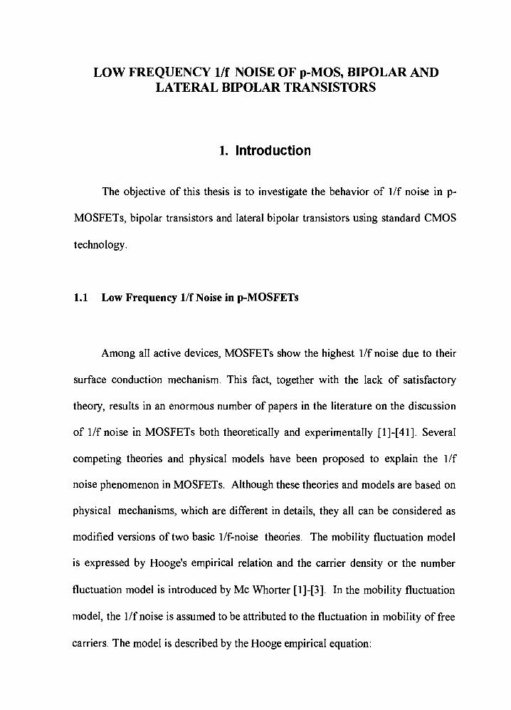
LOW FREQUENCY 1/f NOISE OF p-MOS, BIPOLAR ANDLATERAL BIPOLAR TRANSISTORS
1. Introduction
The objective of this thesis is to investigate the behavior of 1/f noise in p-
MOSFETs, bipolar transistors and lateral bipolar transistors using standard CMOS
technology.
1.1 Low Frequency 1/f Noise in p-MOSFETs
Among all active devices, MOSFETs show the highest 1/f noise due to their
surface conduction mechanism. This fact, together with the lack of satisfactory
theory, results in an enormous number of papers in the literature on the discussion
of 1/f noise in MOSFETs both theoretically and experimentally [1]-[41]. Several
competing theories and physical models have been proposed to explain the 1/f
noise phenomenon in MOSFETs. Although these theories and models are based on
physical mechanisms, which are different in details, they all can be considered as
modified versions of two basic 1/f-noise theories. The mobility fluctuation model
is expressed by Hooge's empirical relation and the carrier density or the number
fluctuation model is introduced by Mc Whorter [1]-[3]. In the mobility fluctuation
model, the 1/f noise is assumed to be attributed to the fluctuation in mobility of free
carriers. The model is described by the Hooge empirical equation:
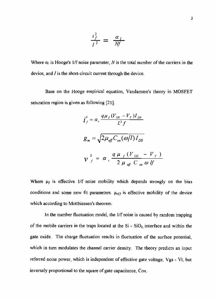
2
.2lj a1
j2Nf
Where a1 is Hooge's 1/f noise parameter, Nis the total number of the carriers in the
device, and I is the short-circuit current through the device.
Base on the Hooge empirical equation, Vandamm&s theory in MOSFET
saturation region is given as following [21].
.2=
q,u1(V VT)JDS
L2f
g,, = f2PeffCox(W/l)IDS
2 q/Jf(VGS VT)Vf= a, 2effCoxf
Where .t1 is effective 1/f noise mobility which depends strongly on the bias
conditions and some new fit parameters. Re!! is effective mobility of the device
which according to Motthiessen's theorem.
In the number fluctuation model, the 1/f noise is caused by random trapping
of the mobile carriers in the traps located at the Si - Si02, interface and within the
gate oxide. The charge fluctuation results in fluctuation of the surface potential,
which in turn modulates the channel carrier density. The theory predicts an input
referred noise power, which is independent of effective gate voltage, Vgs - Vt, but
inversely proportional to the square of gate capacitance, Cox.

3
In the last four decades, a considerable number of papers have been published
dealing with 1/f noise in MOSFETs. Research has focused on resolving these two
theories, but has not provided any satisfactory resolution. Inconsistent
experimental results were reported for both the n- and p-MOSFET devices. Also,
different 1/f noise MOSFETs models were introduced in different simulation tools,
such as P SPICE and HSPICE. None of these tools has explained which model is
more appropriate for n-MOS and p-MOS, and which one is most appropriate for
use in the MOSFETs with different effective channel lengths and operation regions.
1.2 Low Frequency 1/f Noise in PNP Bipolar Transistors
The theory of low frequency 1/f noise performance of the bipolar junction
transistor has existed for many years [42]-[44]. Although the theoretical treatment
of the 1/f noise in BJT is as difficult as it is for MOSFETs, little attention has been
paid to the fact that 1/f noise of BJT's is less than that of MOSFET's. This is
mainly due to the fact that 1/f noise in BJT is several decades lower than that in
MOSFET transistors. Low frequency noise sources of BJT transistor are shown in
figure 1.1. There are two shot noise sources in BJT junction transistor. One is in
the base area, which is parallel with the base-emitter junction of the BJT. Another
is the collector shot noise source, which is parallel to the collector-emitter terminal
of the BJT. The thermal noise source is associated with the extrinsic base
resistance of the device. The low frequency 1/f noise source of the bipolar junction

4
transistor is a flicker noise generator in parallel with the emitter-base junction of
the transistor.
Note: eb: Thermal noisei: 1/f noisei: shot
Fig. 1.1 Noise sources in bipolar transistors
As mentioned in the discussion of the 1/f noise mechanisms in MOSFETs,
two fluctuation mechanisms may be responsible for the observed 1/f noise.
Researchers trying to explain the noise in bipolar transistors have also used these
two 1/f-noise models, The application of the mobility fluctuation model to BJT is
based on the Einstein relation between mobility and the diffusion constant D as D =
kT/qp, where k, T, p, and q represent the Boltsman constant, room temperature,
mobility, and electron charge respectively. The fluctuation in mobility gives rise to
fluctuation in the diffusion constant, which in turn results in fluctuation in the
diffusion current. The application of the number fluctuation 1/f noise model
assumes that the number fluctuation is due to either a generation-recombination
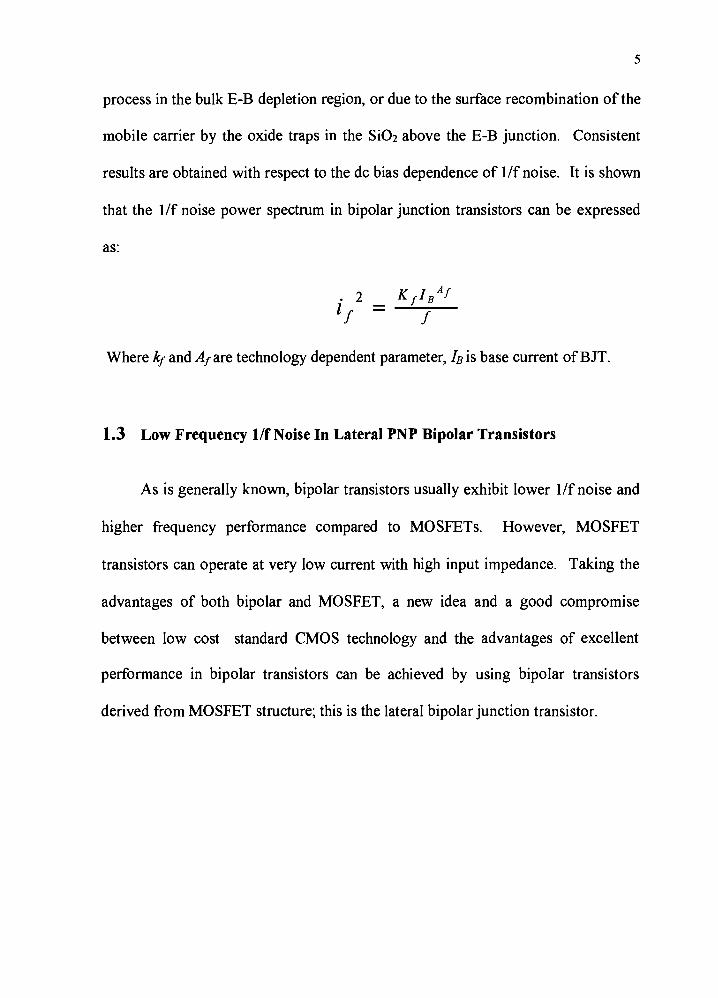
process in the bulk E-B depletion region, or due to the surface recombination of the
mobile carrier by the oxide traps in the Si02 above the E-B junction. Consistent
results are obtained with respect to the dc bias dependence of 1/f noise. It is shown
that the 1/f noise power spectrum in bipolar junction transistors can be expressed
as:
2 KJIBAfiff
Where kf and Ajare technology dependent parameter, IBiS base current of BJT.
1.3 Low Frequency 1/f Noise In Lateral PNP Bipolar Transistors
As is generally known, bipolar transistors usually exhibit lower 1/f noise and
higher frequency performance compared to MOSFETs. However, MOSFET
transistors can operate at very low current with high input impedance. Taking the
advantages of both bipolar and MOSFET, a new idea and a good compromise
between low cost standard CMOS technology and the advantages of excellent
performance in bipolar transistors can be achieved by using bipolar transistors
derived from MOSFET structure; this is the lateral bipolar junction transistor.

2. Low Frequency 1/f Noise in p-MOSFETs
2.1 Measurement Principles
The method for measuring 1/f noise in the semi-conductor devices is to
evaluate the physical quantity of noise, which can be the current or voltage of the
device under tested. One can characterise x (t) by using the Fourier transform
which is given below:
x2Q) = fs(f)df
s (1) 4fx(t)(t + s) cos(cus)th
Once s, (t) is measured, then power density can be calculated. The block
diagram for its measurement is shown in Figure 2.1.
From the Fig. 2.1, the 1/f noise is sampled on the output terminal of the first
block, then amplified on the second block, and only the low frequency 1/f noise is
passed by the third block. Finally it is checked with a multi-meter on the last
block. The sample data represents either voltage or current. Based upon the Fig
2.1, the circuit schematic used to measure 1/f noise in p-MOS transistors is given in
Figure 2.2.
The p-MOS transistor is connected with positive power supplies to its gate
(Vgg) and source (Vss), and the drain is connected to the ground by a load resistor.
This makes the dc component of the sample voltage drop on the load resistor as

7
small as possible. It also reduces power supply noise on the load resistor. The dc
part of the sample voltage can be canceled by common mode rejection of the input
of the op-amp. Then, the weak 1/f noise signal can be amplified by a first order op-
amp filter with a voltage gain of45 and corner frequency of 21 kHz. The digital
multi-meter sampling frequency is 26 Hz. A fourth order Butter-worth filter is
needed to provide a gain of 2 and corner frequency of 4.2 Hz to match the sample
rate of the DMM. The measurement system can provide a total voltage gain of 90
with 4.2 Hz corner frequency. The system background noise is measured by
turning off the p-MOS transistor. The data from the digital multi-meter is
transmitted to the computer via an IEEE BUS port, which is used to interface
between the multi-meter and the computer. The computer is used to set up the data
bus, set the sample rate for the multi-meter, read data, and save it to the data file.
The output 1/f current noise time domain and 1/f current noise density can be
calculated and displayed by a MATLAB program. The 1/f voltage noise density
can be processed and displayed by an EXCEL program.

Device Under Gain Low Pass DigitalTest Amplifier Filter Multi-Meter
Fig. 2.1 Block diagram for the theory of 1/f noise measurement
Fig. 2.2 Schematic diagram of the 1/f noise measurement system in PMOStransistors

9
2.2 p-MOSFET 1/f Noise PSPICE Simulation
The 1/f noise simulation was performed on PSPICE. Two of the noise
models were chosen. The PSPICE device level 3 model is used for the long
channel p-MOS simulation and the PSPICE device level 6 model is used for the
short channel p-MO S simulation in accordance with the P SPICE manual and recent
publications [1]-[41].
The simulation results of the DC characteristics, which include drain current
and transconductance, closely match the data from the tested devices. The noise
characteristics corresponding to the experimental results can be simulated using the
appropriate noise equation selector (NLEV), flicker noise exponent (AF) and
coefficient (KF) in SPICE (see Table 2.1 for details about the device models and
noise models).
2.3 Results and Discussions
Both the long channel p-MOS device (L = 5.0 p.m) and the short channel p-
MOS devices (L = 1.2 .tm and 0.6 m) were measured in the saturation regions of
operation.
An example of the 1/f noise current in the frequency domain is shown in
Fig. 2.3. The measurement is done with a 5-nm p-MOS transistor with Rload = 100
ohm, Vds = 1 1.3V and Ids = 1.53mA in the saturation region.
10
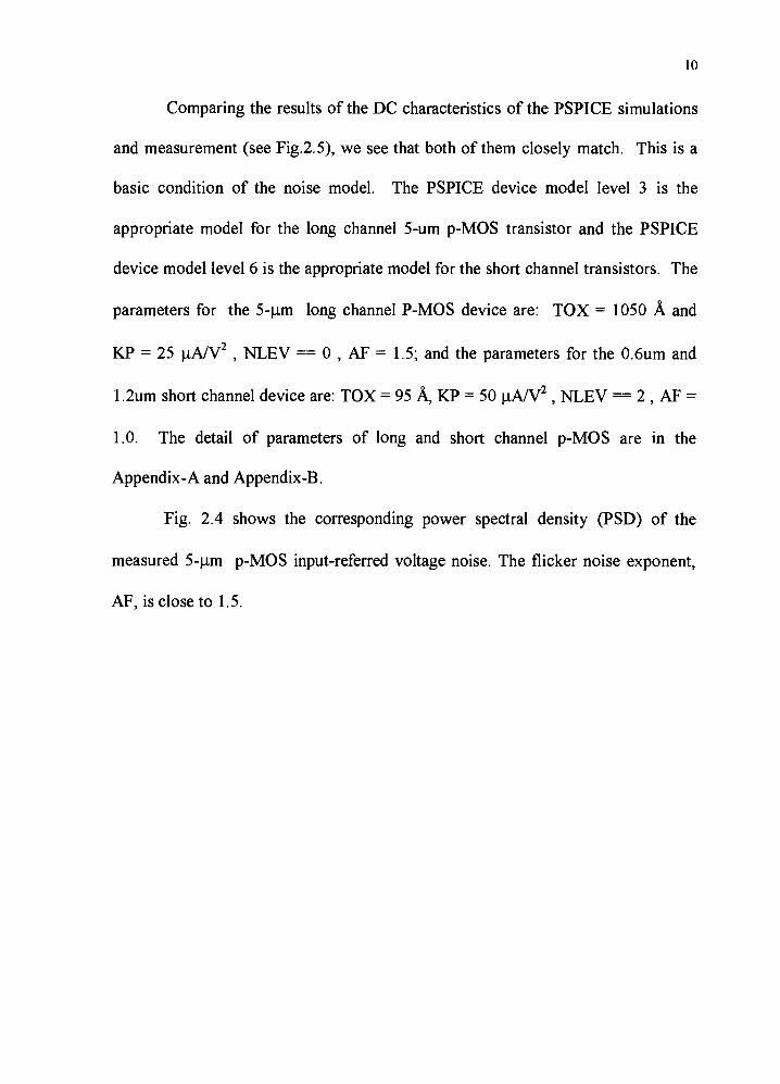
Comparing the results of the DC characteristics of the PSPICE simulations
and measurement (see Fig.2.5), we see that both of them closely match. This is a
basic condition of the noise model. The PSPICE device model level 3 is the
appropriate model for the long channel 5-urn p-MOS transistor and the PSPICE
device model level 6 is the appropriate model for the short channel transistors. The
parameters for the 5-.tm long channel P-MOS device are: TOX = 1050 A and
KP = 25 tA/V2 NLEV == 0, AF = 1.5; and the parameters for the 0.6urn and
1.2um short channel device are: TOX = 95 A, KP = 50 jiA/V2 , NLEV == 2, AF
1.0. The detail of parameters of long and short channel p-MOS are in the
Appendix-A and Appendix-B.
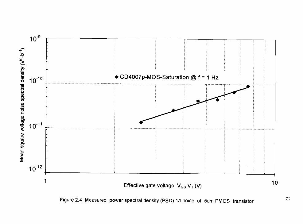
Fig. 2.4 shows the corresponding power spectral density (PSD) of the
measured 5-i.xm p-MOS input-referred voltage noise. The flicker noise exponent,
AF, is close to 1.5.

11
Table 2.1 p-MOSFET noise simulation
Simulation Tools PSPICELevel 3
Device SPICE level 3 (noise model default: NLEV = 2.)Level 6
Model BSIM 3.2 (noise model default: NLEV = 2)KE 1AF
Noise Noise EV = 0 I =COXLeff2fModel
ModelIn JçjJAF
NLEV=1I 2_nd C WeffLefffox
SPICE level 3
NLEV = 2 & 3 (default):
KF.g,2j2nd COXWeffLefffAF
BSIM3.2 Same as above

1010
RiI
-15u, 100CCa)I-
C-)
C-20
t,109-00C))
a-
1025 LbL102 10_i 100 101
Frequency (Hz)
Figure 2.3 5m PMOS 1/f drain current noise in the frequency domainPMOS: W =720 p.m, L =5 pm, Vss = 12 V. Vgs = 5V
12
io-9
NI
U)C0) -10vlO0ci
U)
ci
U)0Ca)0)Co
0>
CU
0U)
CCUa)
1012
IEffective gate voltage VGS-VT (V)
Figure 2.4 Measured power spectral density (PSD) 1/f noise of 5um PMOS transistor

0)0
C
0
10.1
102
-3
io
io50
5um-pmos-measurement
O.6um-pmos-measurement1 .2um-pmos-measurement
o 5um-pmos-simulationo 1 .2um-pmos-simulation
o O.6um-pmos-simulation
2 4 6 8
Geta voltage VGS (V)
Figure 2.5 Measured and simulated DC characteristics of (5, 0.6, 1.2) urn PMOS transistors
10
-a

15
Figure 2.6 shows the simulated and measured p-MOS mean square drain
current noise versus the square of the drain current in the saturation region for L =
5.0 p.m, 1.2 p.m and 0.6 p.m respectively at a frequency of 1.0 Hz. It shows that the
shorter the p-MOS transistor channel, the larger the mean square drain current
noise. It also demonstrates that the mean square drain current noise (md2) is
proportional to the square of the drain current (Ids).
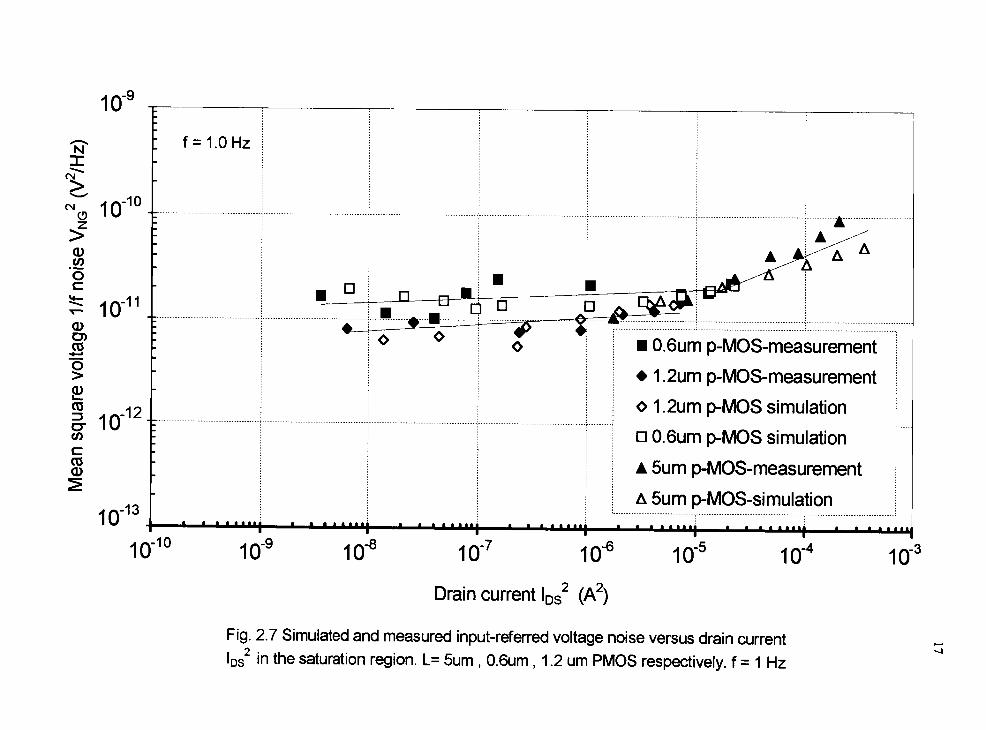
Fig. 2.7 shows the corresponding simulated and measured p-MOS input-
referred voltage noise in the saturation region. It indicates that the input-referred
voltage 1/f noise from simulation also fits that of the measurement.
For both long and short channel devices, from the measured data in Fig. 2.7,
we can see that the mobility fluctuation model (NLEV = 0) is the appropriate
model for long channel devices, since the input referred voltage noise is dependent
on the drain current, and the number fluctuation model (NLEV = 2 ) is the
appropriate model for short channel devices, since the input referred voltage noise
is independent on the drain current.
To summarize the results of simulation and measurement, the 1/f noise
current density and input-referred voltage of p-MOSFET, for long channel devices,
is approximately proportional to the DC bias current 1Ds2. This implies that the 1/f
noise of the p-MOS transistor (long channel) is consistent with the mobility
fluctuation noise model, but for short channel, it is consistent with the number
fluctuation model. Also, it is apparent that short channel transistors or p-MOS
transistors with a small gate area exhibit higher 1/f noise.

1014
Ar15:IU
1)
1O
4-C
° In-17ci)I-(U
C-Cl)
C
1O
0 5um p-MOS-measurement
AO.6um p-MOS-measurement
--H 0 1.2um p-MOS-measurement
1.2um p-MOS-simulation
A O.6um p-MOS-simulation
5um p-MOS-simulation
I flHzI
j----------------r---
.......................................
Pspice Simulation: AF = 1.55um: Level 3 nlevO, KF = 7.84e-27
Simulation: AF = 1.00.6um: Level 6 nlev2 KF = 1.6e-26I .2um: Level 6 nlev2 KF = 4.3e-27
1111111 11111111 Lilt liii IL 111111 Ii 111111 I I
I O I O I O10q
i O i o i o
Drain current lds2 (A2)
Fig. 2.6 Simulated and measured drain current noise versus lds2 in 5.0, 0.6, 1.2 urn PMOS transistors
io
N=
:
a,D)Co
0>2Co
U)
CCoa)
io-9
f1.OHz:
uDf
1013
.
O.6um p-MOS-measurement
I .2um p-MOS-measurement
1 .2um p-MOS simulation
o O.6um p-MOS simulation
A 5um p-MOS-measurement
t 5um p-MOS-simulationa .a.a.i a a a .aaa.j a a p aaa.aj a a I IIpI
I O I O i O i o i o i o i o
Drain current 'Ds (A2)
Fig. 2.7 Simulated and measured input-referred voltage noise versus drain current'DS in the saturation region. L= 5um, O.6um, 1.2 urn PMOS respectively. f = 1 Hz
I L'

18
3. Low Frequency 1/f Noise in Bipolar PNP Transistors
3.1 Measurement Principles
The principles of low frequency 1/f noise measurement in bipolar devices
are the same as with 1/f noise measurement in MOSFET devices. This is shown in
Figure 2.1, "Block diagram for the theory of 1/f noise measurements" (page 8), and
Figure 2.2, "schematic diagram of 1/f noise measurement system in p-MOS
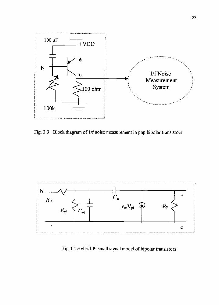
transistors" (page 8). Figure 3.1 and Figure 3.2 shows the block diagram of 1/f
noise analog measurement system for the pnp bipolar transistors. Figure 3.3 shows
the block diagram of 1/f noise automatic measurement system for the pnp bipolar
transistors.
3.2 Low Frequency 1/f Noise Models-Current Dependent Component
For system analysis, the Hybrid-Pi small signal transistor model was chosen
as for this study. (See Figure 3.4) This model provides both an accurate description
of the performance of the bipolar transistor over a wide frequency range, and
insight into the physical processes, which occur in the transistor. Figure 3.4 shows
the noise model based on the Hybrid-Pi model of the transistor. There are four
noise generators: two shot noise, one 1/f noise, and one thermal noise, which are
represented by 'b, i and eb respectively. The ib is a shot noise generator in the
base circuit and i is a shot noise generator in the collector circuit.
19
The noise expressions are as follows:
1. shot noise in the base:2
lb =2qIdf2. shot noise in the collector:
2
i =2qIdf3. thermal noise:
2
eb =4kTRBdf4. low frequency 1/f noise:
2
i., =kIdf/f
Where q: electronic charge constant, 'C collector current of BJT, 'B: base current of
BJT, 1: absolute temperature, RB: base resistor, and k: Boltzman constant.
For low frequency, the noise model of Fig. 3.5 may be considerably
simplified. At low frequency, the effects of C,1 and C are very small, and they can
be taken out of the model. Fig 3.6 shows a simplified low frequency noise small
signal-Pi bipolar transistor model. This model shows a strong correlation between
the flicker noise and non-ideal component of the base current. It was concluded
that the flicker noise could be modeled as a single noise current generator placed
between the emitter and base junctions of the device. In the formula of the low
frequency flicker noise (4), the constant K is related to the base-emitter contact
region, ii, represents the non-ideal portion of the forward base current, df is the
measurement bandwidth. The results of research shows the number fluctuation 1/f
noise model is more favorable to bipolar devices [42]-[44}. The number fluctuation
is assumed to be due to either a generation-recombination process in the bulk E-B
depletion region, or to the surface recombination of the mobile carriers by the oxide

20
traps in the Si02 above the E-B area. More recent work has suggested that trapping
at residual oxide interface, between the poly-silicon and single crystal material
contributes significantly to the noise current, and it is also known from studies of
poly-silicon resistors that grain boundary effects in the emitter can also add to the
low frequency excess noise. A summary of the noise factors shows that the most
important geometrical parameter of a BJT transistor that affects the electrical
behavior is the active emitter area, AE. The 1/f noise power spectrum in BJT can be
expressed as:
2 KJ.JBAJiff
Where Kf and Af are technological dependent parameters, and 'B is base current of
BJT.

21
+\TDD
EI3
400k C lit AnalogMeasurement
T 100 uF[
I I
System
100 ohmlOOK
Fig. 3.1 Analog 1/f noise pnp bipolar measurement system-i
+VDD
lu AnalogI Measurement
System
Fig. 3.2 Analog 1/f noise pnp bipolar measurement system-2
22
Fig. 3.3 Block diagram of 1/f noise measurement in pnp bipolar transistors
Fig 3.4 Hybrid-Pi small signal model of bipolar transistors

23
Fig 3.5 Noise model of bipolar transistors
Fig. 3.6 Low frequency noise model of bipolar transistors
24
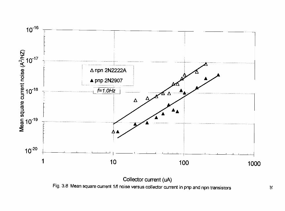
Both npn (2N2222A) and pnp (2N2907) have been measured in the
forward active regions of operation.
An example of the 1/f noise current in the frequency domain is shown as
Figure 3.7. The measurement is done with a pnp (2N2907) bipolar transistor with
Rload = 100 ohm, V = 5.15 V and I = 1 mA in the forward active region.
Figure 3.8 shows an automatic measurement of the npn and an pnp bipolar
transistor 1/f current noise versus collector current in the forward active region at a
frequency of 1.0 Hz. It shows that the results of the 1/f noise of npn and pnp
transistor are identical with the results of 1/f noise which were calculated from the
formula. As the base current goes up, both pnp and npn 1/f noise also goes up.

1010
NI
a)U)
0CCI-
C-)
0
- i-2°0 "C.)
.4-0
1025
io i02 10_i 100 101 102
Frequency (Hz)
Figure 3.7 PNP (2N2907) transistor 1/f collector current noise in thefrequency domain (Vce = 5.15 V, Ic = 1 mA)
25
1016
N17dO
Cl)
0CI-'
1018
C .ir-l9Cobci)
1020
1
A
10
A
100
Collector current (uA)
Fig. 3.8 Mean square current 1/f noise versus collector current in pnp and npn transistors
I

27
3.3 Low Frequency 1/f Noise Models-Voltage Dependent Component
Many authors have studied the low frequency 1/f noise of bipolar transistor
current dependence model. [42]-[48] One of the original references on 1/f noise in
bipolar transistors, by E.R. Chenette et al., [48] is still used as the basis for
modeling 1/f noise in bipolar transistors (see section 3.2). However, the
publication [48] also described a component, which depended on VCE or the
collector emitter voltage, although no model or equation was given for this
component. This parts of the chapter presents the collector-emitter voltage
dependence model [46]-[47].
From the 1/f noise temperature fluctuation analysis in bipolar transistors
[46]-[47], 1/f noise mean square current can be expressed as:
i=2qI( )2(AT)2(OCth)
KT/q T w
Where 2q1 is the shot noise, and Wcth is corner frequency of 1/f noise.
Let assume both (A V/VT) and (AT/i) are constant, the result is that the 1/f
noise current spectral density is proportional to Ji/ .O. From the results of analog
measurement, the corner frequency can be obtained. Then, it is easy to calculate the
1/f noise value from the analog measurement region to the automatic measurement
region. The effective device area also can be calculated by the formula
28
A2( LV )2041(VCeI)
KT/q T a
The results of the experiments from the analog and automatic measurements
show that the corner frequencies are 40 KHz and 70 KHz respectively. The active
areas are 4.386X10⁷ Cm2 and 4.573X10⁷ Cm2, which corresponding with the 40
kHz and the 70 kHz frequency, are the reasonable values for these bipolar
transistors.
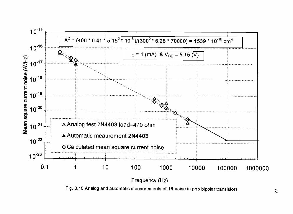
Figure 3.9 and Figure 3.10 show collector current 1/f noise frequency
domain for two pnp and one npn bipolar transistors in the (Vce=5.15V and
Ic= 1 mA) forward active region by analog and automatic measurement.
At a low frequency, i.e. f < 10 kHz, the transistor noise spectral density
shows the well known 1/f distribution. In the experiment, two of the 1/f noise
measurement methods are used to confirm the theory is consistent with the results
of measurement. The analog measurements focus on the frequency region from 700
Hz to 5 kHz, and automatic measurement focuses on the frequency region 0.5 Hz to
1 Hz. The results of the measurements show that the trend of 1/f noise in pnp and
npn bipolar transistors is consistent from the analog testing frequency region to the
automatic testing frequency region.
Fig. 3.11 shows the corresponding measured npn and pnp bipolar transistor
1/f noise power special current density in the forward active region at I kHz, while
maintaining the same collector current but varying collector voltage. The result
shows that 1/f noise mean square current depends on the collector voltage.

1015
.4I1O
I O
i ü
A2 = (400 * 0.41 * 5.152* 10)/(3002* 6.28 * 40k) = 1924 * 1016 cm4
I
k = 1 (mA) & VCE = 5 15 (V)
rULUuIIOLI LOL
Calculated mean square current noiseo Analog test 2N2222A Load=1 00 ohmiAutomatic test 2N2222A
I I I llIlj I IIIII I I II IIIIj I I I III
0.1 I 10 100 1000 10000 100000 1000000
Frequency (Hz)Fig. 3.9 Anolog and automatic measurements of 1/f noise in pnp and npn bipolar transistors
1015
1016
Ni: -17
U)
.SQ -18o10
1019
1 022
1023
0.1 1 10 100 1000 10000 100000 1000000
Frequency (Hz)
Fig. 3.10 Analog and automatic measurements of 1/f noise in pnp bipolar transistors 0

1016
4f17.-' luN
ci) IA-18U) IV0C
10
c -20
0U)
CCoci)
10-
I 0
1 10 100
Collector and emitter voltage VCE (V)
Fig. 3.11 Analog measurements of 1/f noise in pnp and npn bipolar transistors

32
3.4 Conclusion
In conclusion for this chapter, the results of 1/f noise measurement and
results of 1/f noise calculated from 1/f noise voltage dependence theory confirm the
1/f noise behavior of noise in bipolar junction transistors. It shows a 1/f
distribution in the low frequency region. The experimental data fits the theory very
well at some points from 1 Hz to 5 kHz low frequency 1/f noise region. However in
very low frequency region, such as f < 1 Hz, more research works should be done
to investigate that region. The 1/f noise is also depend on collector voltage which
was found in the 1/f noise measurement of bipolar transistor.
33
4. Low Frequency 1/f Noise in Lateral PNP Transistors
4.1 Measurement Principles
The principles applied for low frequency 1/f noise measurement on the
lateral pnp bipolar devices are the same as those used for 1/f noise measurement on
MOSFET devices. The only difference is the different configuration on the p-
MOSFET transistor, which turns off the p-MOS transistor and turns on the lateral
pnp devices. For the system configuration, refer to Figure 2.1 "Block diagram for
the theory 1/f noise measurements" (page 8), and Figure 2.2 "Schematic diagram
the 1/f noise measurement system in p-MOSFET transistors" (page 8). Figure 4.1
shows the block diagram of 1/f noise measurement system for lateral pnp bipolar
transistors.
Figure 4.1 presents the lateral pnp device in long channel p-MOSFET
transistors. The configuration of lateral pnp for the short channel p-MOSFET
transistors is the same as that of long channels ones.
4.2 DC Characteristics of Lateral PNP Transistors
Figure 4.2 shows the basic structure of the lateral pnp bipolar transistor,
which includes one lateral and two vertical parasitic bipolar transistors that are
inherently available in standard CMOS technology. Considering standard CMOS
technology, the typical structure of a lateral pnp transistor is depicted in Figure 4.2.
34
In addition to the horizontal lateral transistor, two vertical parasitic devices can be
identified in this composite structure. If the lateral transistor is biased in its forward
region, one of the vertical transistors will work in the forward region. Due to fact
that the substrate is always tied to the most negative voltage in the circuits, the
holes injected from the emitter region toward the n-well, which plays the role of the
base for both the lateral and vertical pnp, will be just partially collected at the
collector terminal of the lateral device. In fact, an appreciable fraction of them will
reach the collector of the vertical transistor, that is the substrate. Due to the
physical structure of CMOS, there are three input terminal protection diodes. In
order to make the lateral pnp work correctly, the configuration of the system will
have to solve two problems: First, the p-MOS is approximately turned off, and
second, all of the protection diodes should be close to cut off. A small DC bias
source is used to obtain the bias conditions described above. The total 1/f noise of
the lateral pnp in p-MOSFET transistor, should include the noise coming from one
of the horizontal lateral pnp and one of two vertical pnp's and depends on the
circuit bias set up.
Details of the DC bias set up of the 1/f noise measurements for lateral pnp
transistors are shown in Fig. 4.1 and Fig 4.2. From the circuit DC set up, the
emitter connects to the positive power supply, the collector connects to ground, the
base is connected through a resistor to ground, and the substrate connect to
collector. For the horizontal lateral pnp transistor, emitter is connected to VDD,
and the base voltage is about 0.7 volts lower than the emitter. The base-emitter
35
junction is forward biased, and base-collector junction is reverse biased. This puts
the lateral pnp operating in the forward active region. For left side vertical lateral
pnp, the emitter is connected to VDD, the substrate is connected to the collector,
and the base is set to about 0.7 volts lower than the emitter, the pnp transistor is
operating in the forward active region. For the right side vertical lateral pnp
transistor, the emitter is connected to ground, the base voltage is higher than the
emitter, and the substrate is connected to the collector. This lateral pnp is in the cut
off region. The total 1/f noise sample from the lateral pnp should include the
horizontal lateral pnp and one of the vertical lateral pnp transistors. The most of the
1/f noise in this lateral pnp structure come from the horizontal lateral pnp. The
reasons are as follow: n-well, source and drain form the horizontal lateral pnp;
source or drain, n-well and substrate form the vertical lateral pnp. The vertical
conduction current is much smaller than that of the horizontal one.

Rb
Gnd
- 1.5V+
+VDD
Gate (Pin 10)
Base. (Pin 14)
Collector (Pin 11)
Emitter ( Pin 12)
Substrate ( Pin 7)
1K
36
Note: 1. For turn off the p-MOS, V1 1.4V, Vos <VT : Let VGB= O.4VSince VEB = O.7V VEG = O.7V-O.4V = O.3V, p-MOS is in cutoff region.
2. Since VBG = O.4V, the protection diode between the gate toN-well is cut off.
Fig. 4.1 The circuit for 1/f noise measurements in lateral pnp transistors

Source Gate DrainSubstrat (Emitter) (Collector)
......:::::::::::.
I IP !I P+
....................Base
P
p-substrate
37
Bulk(Base)
N-well
1, Lateral bipolar transistor: Emitter (source), Collector (drain), Base (N-well)2. Vertical parasitic bipolar transistor: Emitter (source), Collector (P-sub.), Base (N-well)3. Vertical parasitic bipolar transistor: Emitter (drain), Collector (P-sub.), Base (N-well)
Fig. 4.2 Basic lateral pnp transistor structure in p-MOSFET's
38
4.3 Results and Discussions
Figure 4.3 is the plot of the lateral pnp collector current versus base voltage
using 5um, O.6um and 1 .2um p-MOS devices. The plot shows the basic DC
characteristic of the pnp bipolar transistor.
Figure 4.4. is the plot of lateral pnp gain versus base resister using 5um,
O.6um and 1 .2um p-MOS devices. This plot shows the gain results of the lateral
pnp configuration in the p-MOS devices.
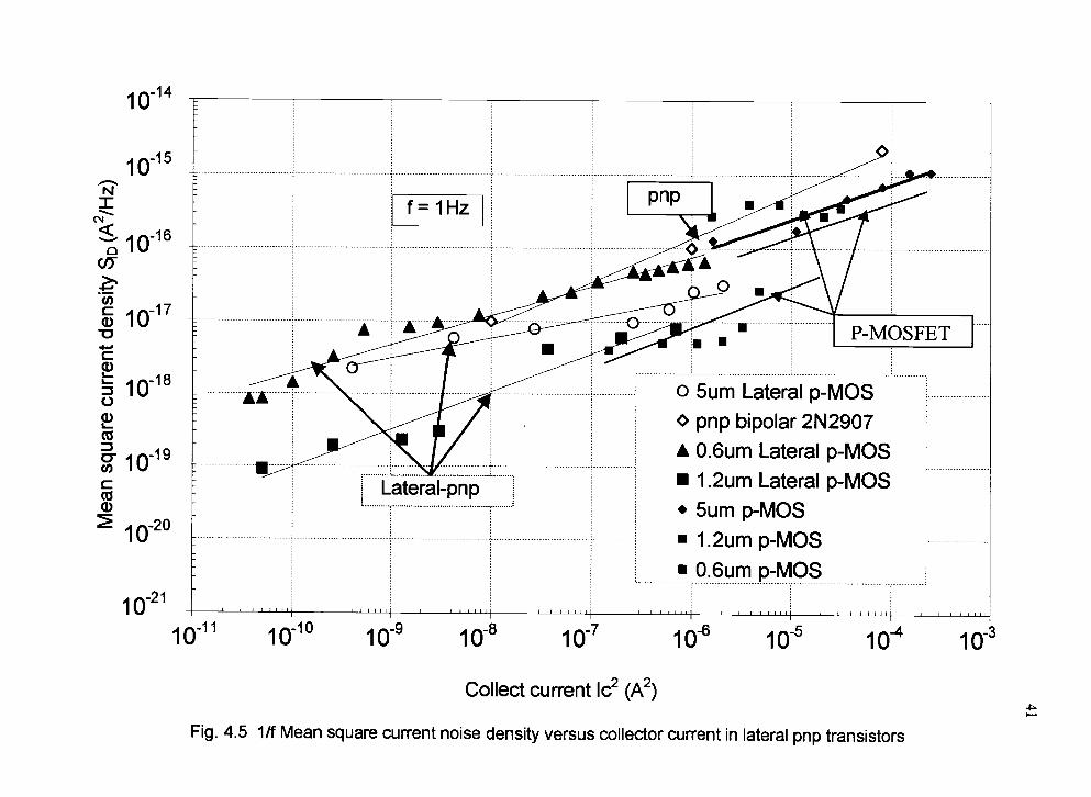
Figure 4.5 shows 1/f noise current density of the lateral pnp in p-MOS. It
compares the results of a commercial pnp device (2N2907) and long and short
channel p-MOSFET devices (CD-4007, Bpm 106 and Bpml 12 which are 5um,
0.6um and 1 .2um respectively).

10-
io
110.4
io
1O.61
0.50 0.55 0.60 0.65 0.70 0.75 0.80 0.85
Base voltage VBE (V)
Fig. 4.3 Collector current versus base voltage of lateral pnp transistors (0.6, 1.2, 5 ) urn
LI'J

(I)
0U)
U)
0C
CDI-a)4-,CD
9-0CCo
0
100
10
I
io io io io
Collect current I (A)
Fig. 4.4 Lateral pnp transistor current gain versus collector current
102
C
1014
1O
I..)liIllil 111111111 liii 11111 lIllilIll IlillIll Ill trill Ii 1111111
I41
1 I O I O i o i o i o i
Collect current Ic2 (A2)
Fig. 45 1/f Mean square current noise density versus collector current in lateral pnp transistors
io
42
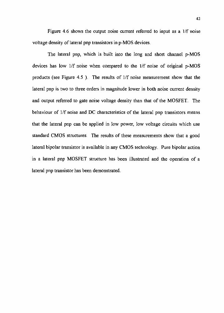
Figure 4.6 shows the output noise current referred to input as a 1/f noise
voltage density of lateral pnp transistors in p-MOS devices.
The lateral pnp, which is built into the long and short channel p-MOS
devices has low 1/f noise when compared to the 1/f noise of original p-MOS
products (see Figure 4.5 ). The results of 1/f noise measurement show that the
lateral pnp is two to three orders in magnitude lower in both noise current density
and output referred to gate noise voltage density than that of the MOSFET. The
behaviour of 1/f noise and DC characteristics of the lateral pnp transistors means
that the lateral pnp can be applied in low power, low voltage circuits which use
standard CMOS structures. The results of these measurements show that a good
lateral bipolar transistor is available in any CMOS technology. Pure bipolar action
in a lateral pnp MOSFET structure has been illustrated and the operation of a
lateral pnp transistor has been demonstrated.
io-g
Ri' jr-10II'-,(N>(N
>z1O
>%
Cl)
C1)
0G) 1rr12Q)
0Cci)
1O
1015
5urnLateralp-MOS -:0 O.6um Lateral p-MOS0 1 .2um Lateral p-MOS0 pnp bipolar 2N2907.5ump-MOSa1.2um p-MOS.O6um p-MOs
Jn
+ ---------------------------------------
f=1.OHzI
10h1 10b0 108 iO io io
Collector current Ic2 (A2)
Fig. 4.6 1/f Mean square voltage noise density versus collector current in lateral pnp transistors
io-4 io

44
Chapter 5 Conclusions
In this thesis, a If noise analysis is performed for three different
technologies: the MOSFETs, the standard bipolar transistors and the lateral pnp
bipolar transistors. From these analyses, the theoretical lowest limits of 1/f noise
levels can be achieved by the three different technologies. In order to obtain insight
into the details of the noise behavior of MOSFET transistors and BJT transistors,
both theoretical and experimental studies of 1/f noise in MOSFET and BJT are
presented. The emphasis has been to compare the results of tests with theory,
analyze them, and to draw conclusions.
Summary two of basic 1/f noise theory in MOSFET, the carrier number
fluctuation theory predicts an input referred 1/f noise power which is independent
of the effective gate voltage, but inversely proportional to the capacitance, Cox. It
is given by the PSPICE level two 1/f noise equation (NLEV = 2); the mobility
fluctuation theory predict an input referred 1/f noise power which is dependent of
the effective gate voltage, inversely proportional to the gate capacitance, Cox. It is
given by the PSPICE level zero 1/f noise equation (NILEV = 0). The results of 1/f
noise measurement and simulation indicate that the low frequency 1/f noise in long
channel p-MOSFETs is proportional effective gate voltage and the low frequency
1/f noise in short channel p-MOSFET do not depend on the effective gate voltage.
This suggests that the flicker noise in long channel p-MOSFETs follows the
mobility fluctuation and the flicker noise in short channel p-MOSFETs follows

45
carrier density fluctuation. The reason of the two different results for the long and
short channel p-MOSFETs structure might be because of the short channel effect.
For the bipolar transistor, the 1/f noise is assumed to be due to the surface
recombination of the mobile carriers by the oxide traps in the SiO2 above the E-B
junction or due to a generation-recombination process in the bulk E-B depletion
region. Since in the modem BJT transistors the total base current flows mainly in
the bulk region, the surface 1/f noise is much smaller than the generation-
recombination 1/f noise, so that the surface 1/f noise can be neglected. Therefore
the 1/f noise power spectral density of bipolar transistor depend on the magnitude
of the base current, on the area of the emitter, and on the base width.
Our results of 1/f noise measurement in bipolar transistor shows that 1/f noise
in bipolar transistor is strongly dependent of the base current or collector current.
This is the basic 1/f noise current dependence model in bipolar transistor. On the
other hand, the data from our measurement also indicates that 1/f noise in bipolar
transistor not only depends on the collector current but also depends on the
collector voltage in the frequency region 1 Hz to 1 KHz.
The measurement of 1/f noise in lateral pnp bipolar transistors in CMOS
technology is discussed. It shows that the lateral bipolar transistor has the
advantage of lower 1/f noise compared to the CMOS devices. The measurements
also give the 1/f noise dependence of discrete bipolar transistors and show that they
are comparable.

46
BIBLOGRAPHY
[1] A. L. McWhorter, "1/fnoise and germanium surface properties," SemiconductorSurface Physics, R.H. Kingston, Ed., Philadelphia, PA: Univ. of Pennsylvania Press,pp. 207-228, 1957.
[2] F. N. Hooge, "1/fnoise is no surface effect," Phys. Lelt., vol. A-29, pp. 139-140,1969.
[3] F. N. Hooge, "1/f noise," Physica, vol. 83B, pp. 14-23, 1976.
[4] L. K. J. Vandamme and H. M. M. Werd, "1/fnoise model for MOSTs biased innonohmic region," Solid-State Electronics, vol. 23, pp. 325-3 29, 1980.
[5] H. S. Park, A. Van Der Ziel and S. T. Liu, "Comparison of two 1/f noise models inMOSFETs," Solid-State Electronics, vol. 25, no. 3, pp. 213-217, 1982.
[6] G. Reimbold, "Modified 1/f trapping noise theory and experiments in MOStransistors biased from weak to strong inversion-influence of interface states," IEEETransactions on Electron Devices, vol. ED-31, no. 9, pp.1190-1 198, Sept. 1984.
[7] G. Nicollini, D. Pancini and S. Pernici, "Simulation-oriented noise model for MOSdevices," IEEE Journal of Solid-State Circuits, vol. SC-22, no. 6, pp. 1209-12 12,Dec. 1987.
[8] Y. Tsividis, "Operation and modeling of the MOS transistor," McGraw- Hill Inc., pp.340, 1987.
[9] A. van der Ziel, "Unified presentation of 1/fnoise in electronic devices: Fundamental1/f noise sources," Proc. IEEE, vol. 76, no. 3, pp.233-258, March 1988.
[10] K. K. Hung and P. K. Ko, "A Unified Model For the Flicker Noise in Metal-OxideSemiconductor Field-Effect Transistors," IEEE Transactions On ElectronDevices, vol. 37, no. 3, pp. 654-664 March 1990.
[11] T. Elewa and B. Boukriss, "Low-frequency noise in depletion-mode DIMOXMOS transistors," IEEE Transactions on Electron Devices, vol. 38, no. 2, pp. 323-327, Feb. 1991.
[12] J. T. Hsu and J. Wang, "Flicker noise in thin film depleted SOT MOSFETS," IEEEDevice Research Conference, pp. 30-3 1, 1991.
47
[13] S. Fang and J. P. McVittie, "Thin-oxide damage from gate charging during plasmaprocessing," IEEE Electron Device Letters, vol. 13, no. 5, pp. 288-290, May 1992.
[14] C. H. Cheng and C. Surya, "The effect of hot-electron injection on the propertiesof flicker noise in n-channel MOSFETs," Solid-State Electronics, vol. 36, no. 3,pp. 475-479, 1993.
[15] D. M. Fleetwood and P. S. Winokur, "Effects of oxide traps, interface traps, andborder traps on metal-oxide-semiconductor devices," J. Appl. Phys, vol. 73, no.10, pp. 5058-5072, May 15, 1993.
[16] M. Tsai and T. Ma, "1/fnoise in hot-carrier damaged MOSFET's: effects of oxidecharge and interface traps," IEEE Electron Device Letters, vol. 14, no. 5, May 1993.
[17] P. R. Gray and R. G. Meyer, "Analysis and Design of Analog Integrated Circuits,"Third edition, John Wiley & Sons, Inc., 1993.
[18] D. M. Fleetwood, 1. L. Meisenheimer and J. H. Scofield, "1/fnoise and radiationeffects in MOS devices," IEEE Trans. on Electron Devices, vol. 41, no. 11, pp.1953-1964, Nov. 1994.
[19] J. Chang, A. A. Abidi and C. R. Viswanathan, "Flicker noise in CMOS transistorsfrom subthreshold to strong inversion at various temperatures," IEEE Trans. onElectron Devices, vol. 41, no. 11, pp. 1965-1971, Nov. 1994.
[20] J. H. Scofield and N. Borland, "Reconciliation of different gate-voltagedependencies of 1/fnoise in n-MOS and p-MOS transistors," IEEE Transactionson Electron Devices, vol. 41, no. 11, pp. 1946-1952, Nov. 1994.
[21] L. K. J. Vandamme, X. Li and D. Rigaud, "1/fnoise in MOS devices, mobility ornumber fluctuations," IEEE Trans. on Electron Devices, vol. 41, no. 11, pp. 1936-1944, Nov. 1994.
[22] C. Hu and G. P. Li, "Low-frequency noise considerations for MOSFET analogcircuits," Abst. IEEE Device Research Conf, Charlottesville, VA, pp. 16-17, 1995.
[23] C. Hu, J. Zhao, G. P. Li, P. Liu, E. Worley, J. White and R. Kjar, "The effects ofplasma etching induced gate oxide degradation on MOSFET's 1/f Noise," IEEEElectron Device Letts., vol. 16, no. 2, pp. 61-63, Feb. 1995.
[24] E. Simoen and C. Claeys, "Correlation Between the Low-Frequency Noise SpectralDensity and the Static Device Parameters of Silicon-on-Insulator MOSFET's," IEEETrans. on Electron Devices, vol. 42, no. 8, pp. 1467-1472, Aug. 1995.
48
[25] M. Aoki and M. Kato, "Hole-induced 1/f noise increase in MOS transistors," IEEEElectron Device Letis., vol. 17, no. 3, pp. 118-120, March 1996.
[26] N. Lukyanchikova, M. Petrichuk, N. Garbar, E. Simoen and C. Claeys, "Back andfront interface related generation-recombination noise in buried-channel SOl p-MOSFET's, "IEEE Transactions on Electron Devices, vol. 43, no. 3, pp. 4 17-423,March 1996.
[27] J. A. Babcock, W. M. Huang, J. M. Ford, D. Ngo, D. J. Sponsor and S. Cheng,"Low-frequency noise dependence of TFSOI BiCMOS for low power RF mixed-model applications," IEEE mt. Electron Device Meeting, pp. 133-136, 1996.
[28] S. S. Chen and S. C. Lin, "Kink effect on subthreshold current conductionmechanism for n-Channel metal-oxide-silicon devices," J. App!. Phys, vol. 80, no.10, pp. 5821-5827, Nov. 15, 1996.
[29] C. Hu, G. P. Li, E. Worley and J. White, "Consideration of low-frequency noise inMOSFET's for analog performance," IEEE Electron Device Letts., vol. 17, no. 12,pp. 552-554, Dec. 1996.
[30] E. Simoen and C. Claeys, "The low-frequency noise behavior of silicon-on-insulatortechnologies," Solid-State Electronics, vol. 39, no.7, pp. 949-960, 1996.
[31] HSPICE User's Manual, Meta-Software, Inc., 1996.
[32] J. A. Babcock, C. E. Gill, J. M. Ford, D. Ngo, E. Spears, J. Ma, H. Liang, D. J.Spooner and S. Cheng, "1/f noise in graded-channel MOSFET's for low-powerlow-cost RFIC's," Abst. IEEE Device Research Conf, Fort Collins, pp. 122-123,1997.
[33] T. Boutchacha, G. Ghibando, G. Guegan and T. Skotnicki, "Low frequency noisecharacterization of 0.18 urn Si CMOS transistors," Microelectron Reliab., vol. 37,no. 10/11, pp. 1599-1602, 1997.
[34] T.Boutchacha, G. Ghibando, G. Guegan and M. Haond, "Low frequency noisecharacterization of 0.25 urn Si CMOS transistors," .1. of Non-Crystalline Solids, vol.216, pp. 192-197, 1997.
[35] M. J. Chen and J. S. Ho, "A three-parameter-only MOSFET subthreshold currentCAD model considering back-gate bias and process variation," IEEE Trans. onComputer-Aided Design of Integrated Circuits and System, vol. 16, no. 4, pp. 343-352, April 1997.
49
[36] Daniel P. Foty, "MOSFET modeling with SPICE: principles and practice,"Prentice-Hall, Inc., 1997.
[37] PSPICE Manual, Version 8.0, MicroSim Corporation, June 1997.
[38] C.T. Liu, D. Misra, K. P. Cheung, G. B. Alers, C. P. Chang, J. I. Colonell, W. Lai, C.S. Pai, R. Liu and J. 1. Clemens, "Reduced 1/f noise and gm degradation for sub-0.25um MOSFETs with 25 -50 gate oxides grown on nitrogen implanted siliconsubstrates," A bst. IEEE Device Research Conference, Fort Collins, CO. pp. 124-125,1997.
[39] J. A. Babcock, D. K. Schroder and Y. Tseng, "Low-frequency noise in nearly-fully-depleted TFSOI MOSFET's," IEEE Electron Device Letts., vol. 19, no.2, pp. 40-43,Feb. 1998.
[40] C. Jakobson, I. Bloom and Y. Nemirovsky, "1/f noise in CMOS transistors foranalog applications from subthreshold to saturation," Solid-State Electronics, vol.42. no. 10, pp. 1807-1817, 1998.
[41] T. Wang and L. P. Chiang, "Characterization of various stress-induced oxidetraps in MOSFET's by using a subthreshold transient current technique," IEEETrans. on Electron Devices, vol. 45, no. 8, pp. 179 1-1796, Aug. 1998.
[42] R C. Jaeger, "Low-Frequency Noise sources in Bipolar Junction Transistors,"IEEE Trans on Electron Devices, vol. ED-17, no. 2, pp 126-134, Feb. 1970.
[43] Michael Stoisiek and Dietrich Wolf, "Origin of noise in Bipolar Transistors, "IEEETrans on Electron Devices, vol. ED-27, no. 9, pp 1753-1756, Sep. 1980.
[44] Mario Conti, "Surface and bulk effects in Low Frequency Noise in NPN PlanarTransistors, "Solid-State Electronics, Pergamon Press, vol. 13. pp. 1461-1469,1970.
[45] W. Timothy Hoiman and J. Alvin Connelly, "A Compact Low Noise OperationalAmplifier for a 1.2 tm Digital CMOS Technology, " IEEE Journal of SolidCircuits, vol. 30, no. 6, pp 710-714, June. 1995.
[46] L. Forbes, " 1/f noise due to temperature fluctuations in heat conduction, "IEEEDevice Research Conference, Santa Barbara, pp. 46-47, June. 1996.
[47] L. Forbes, M.S. Choi and W. Cao," 1/f noise due to temperature fluctuations in heatconduction in bipolar transistors, "Microelectronic Reliability, Vol. 39, No. 9, pp.1357-1364, 1999.

50
[48] J.L. Plumb and E.R. Chenette, "Flicker noise in transistors, "IEEE Trans onElectron Devices, vol. ED-b, pp. 304-308, 1963.

51
APPENDICES

52
The following programs have been used in this research to deal with the
measured noise data and the SPICE simulations.
Appendix A MATLAB Program
This program collects the Digital Multimeter (DMM) data, which is in the
form of voltage variation (unit, V) at the drain of the PMOS transistor in time domain,
and then changes it to the drain current noise (A2IHz) by doing the fast Fourier
transform (FFT). The results were plotted in frequency domain ranging from about
0.01 Hz to 4.2 Hz. Then the average drain current noise at the 1.0 Hz of frequency was
obtained by reading from the figure. There are some notes in the program to help to
understand the program.
% PSD of pmos 1/f noise% data is taken from experimental research lab
clear all; close all
load 'plO6tla7.dat' % PMOS data from Digital Multimeter
Vout plO6tla7; % Unit = Vdate = '6/29/99'; % the date when data is taken
fs=26; % the sampling rate of DI4Ngain=90; % noise amplification ratio by LM741Rload=l0O; % load resistorVnoise = Vout./gain; % PMOS drain voltage noise (V)Inoise = ( Vnoise./Rload); % PMOS drain current noise (A)L = length(Inoise); % L is also a window size. As L get
% larger, the magnitude of fft gets% closer to theoritical val
%SETUP AXISf = fs ( O:1/L:l-1/L ); % up to f=fs (Hz)f = f(1:L/2); % up to fs/2

53
time(O:L-1)/fs;%PSD of NOISEmag = (1/(L*fsfl*abs(mag = mag(1:L/2);
figure (1)
% unit = S
fft(Inoise) ) ."2; % unit = A2/Hz% the desired mean square% drain current noise
% two figures in one page
subplot(2,1,1); % DMM output in time domainplot(time,Vout); grid on;axis([O,200,-O.024,-O.O18]); % axis need to adjusttitle(sprintf('%s (%d pts, %s) ',L,date))xlabel('Time (S)'); % label of the X axisylabel('DMM output (V)'); % label of the Y axiszoom on
subplot (2,1,2);% measured mean square drain current noise in% frquency domain (A2/Hz)
loglog(f,mag,'r'), hold on, grid on,axis([O.O1,1O,le-20,1e--13]); %axis need to adjusttitle('PSD of PMOS Darin Current Noise (A'2/Hz) at
Vgs=2 . 5v')
xlabel ('Frequency (Hz) ');ylabel('PSD of PMOS drain current noise (A''2/Hz)');hold on,loglog(f,le-16./f/'1,'b-.'), % 1/f noise linezoom ongm = 3.9e-3; % measured when Vgs = 4 V for 5-urn PMOSmagi = mag./gm/'2; % change to input-referred noise
figure (2);% measured input-referred voltage noise in frequency% domain (A2/Hz)
loglog(f,magl,'r'), hold on, grid on,axis([O.O1,1O,le-14,le-7]); %axis need to adjusttitle('Power spectral density (PSD) of measured PMOS
input-referred noise.');xlabel('Frequency (Hz)');ylabel (Measured PMOS noise (V"2/Hz) ');hold on,loglog(f,3e-11./f/'1, 'b-.'), % 1/f noise linezoom on
HOLD OFF

54
Appendix B PSPICE Simulation Program for flicker noise
The following programs are used to simulate the 0.6-urn, 1.2-urn and 5-urn
PMOS flicker noise by PSPICE level 6 and level 3. First of all, the transistor DC
characteristics, including the drain current, Ids, and the transconductance, grn, are
matched to the experimental measured data by adjusting the parameters in the PSPICE
rnodels, such as the oxide thickness, TOX, and the intrinsic transconductance
parameter, KP. After that, the noise characteristics can be simulated according to the
noise experirnental results using the appropriate noise equation selector (NLEV),
flicker noise exponent (AF) and coefficient (KF) in PSPICE.
The output file of the PSPICE simulation does not directly give the mean
square drain current noise (md2) and the input-referred voltage noise (Vng2). It gives
the value of FN (output flicker noise at the drain node, V2IHz). We can calculate the
drain current noise and the input-referred voltage noise by the following:
FN(V2 1Hz)42 1Hz) Rload2(12)1nd '/
where Rload is the drain load resistance. In our case, its value is 100 ohms,
2r 2/liz)1nd './V(V2lHz)= gm2(lIc2)
and where gm can be obtained directly from the output file of the PSPICE simulation.
This program is used to simulate the 0.6 urn PMOS flicker noise by PSPICE level 6.
VDD 4 0 dc=-5V % DC power supply at the drain nodeVGS 1 0 dc=-2V ac=1V % DC, AC power supply at the gatenodeRg 1 2 1K % resistive load at the gate nodeRd 3 4 100 % resistive load at the drain nodeCgs 2 0 lOOu % additional gate-source capacitance

ml 3 2 0 0 mosni l=0.6u w=30.8u % PMOS netlist
.MODEL mosni PMOS level=6 tox=95.Oe-lO vto=-0.7v kp=50e-06 % main parameters of DC characteristics
+ nlev=2 af=l kf=2.84e-27.ac dec 100 .01 2.NOISE V(3,0) VGS 10.dc VGS 1 3 0.5.probe % write all.op % calculate
% voltages
55
% noise model parameters% AC analysis% noise analysis% DC analysisanalysis data to output fileand print all dc nodeand voltage source currents
.END % end of PSPICE simulation input file
This program is used to simulate the 1.2 um PMOS flicker noise by PSPICE level 6.
VDD 4 0 dc=-5V % DC power supply at the drain node
VGS 1 0 dc=-2V ac=1V % DC, AC power supply at the gatenodeRg 1 2 1K % resistive load at the gate nodeRd 4 3 100 % resistive load at the drain nodeCgs 2 0 lOOu % additional gate-source capacitance
ml 3 2 0 0 mosni ll.2u w=30.8u % PMOS netlist
.MODEL mosni PMOS level=6 tox=95.Oe-l0 vto=-0.7v kp=50e-06 % main parameters of DC characteristics
+ nlev=2 af=l kf=4.3e-27.ac dec 100 .01 2.NOISE V(3,0) VGS 10.dc VGS 1 3 0.5.probe % write all.op % calculate
% voltages
% noise model parameters% AC analysis% noise analysis% DC analysisanalysis data to output fileand print all dc nodeand voltage source currents
.END % end of PSPICE simulation input file
This program is used to simulate the 5 urn PMOS flicker noise by PSPICE level 3.
VDD 4 0 dc=-12V % DC power supply at the drain node
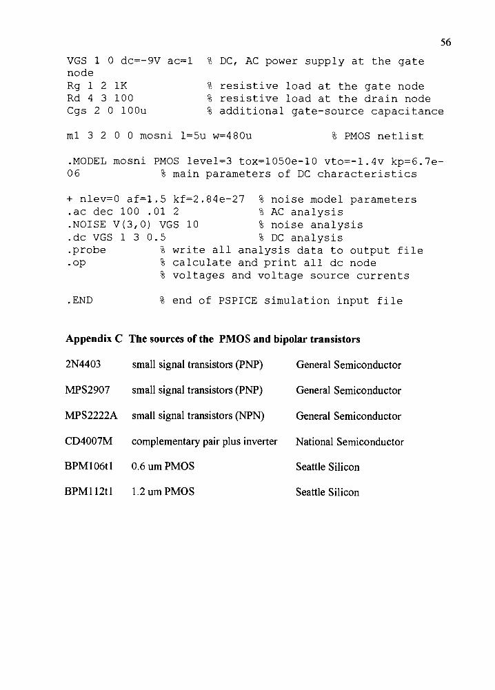
56
VGS 1 0 dc=-9V ac=1 % DC, AC power supply at the gatenodeRg 1 2 1K % resistive load at the gate nodeRd 4 3 100 % resistive load at the drain nodeCgs 2 0 lOOu % additional gate-source capacitance
ml 3 2 0 0 mosni l=5u w=480u % PMOS netlist
.MODEL mosni PMOS level=3 tox=1050e-10 vto=-1.4v kp=6.7e-06 % main parameters of DC characteristics
+ nlev=0 af=1.5.ac dec 100 .01.NOISE V(3,0) V.dc VGS 1 3 0.5.probe %
.op %00
kf=2.84e-27 % noise model parameters2 % AC analysisGS 10 % noise analysis
% DC analysiswrite all analysis data to output filecalculate and print all dc nodevoltages and voltage source currents
.END % end of PSPICE simulation input file
Appendix C The sources of the PMOS and bipolar transistors
2N4403 small signal transistors (PNP) General Semiconductor
MP52907 small signal transistors (PNP) General Semiconductor
M1PS2222A small signal transistors (NPN) General Semiconductor
CD4007M complementary pair plus inverter National Semiconductor
BPM1O6t1 0.6 um PMOS Seattle Silicon
BPM1 12t1 1.2 um PMOS Seattle Silicon