timing uncertainty in sigma-delta analog-to-digital - diva portal
TRANSCRIPT
Timing Uncertainty in Sigma-Delta Analog-to-DigitalConverters
ADAM STRAK
Doctoral DissertationKTH - Royal Institute of Technology
Stockholm, Sweden, 2006

TRITA ICT/ECS AVH 06:11ISSN 1653-6363ISRN KTH/ICT/ECS AVH-06/-12-SEISBN 91-7178-515-9
978-91-7178-515-2
KTH School of Information andCommunication Technology
Isafjordsgatan 39SE-164 40 Kista
SWEDEN
Akademisk avhandling som med tillstånd av Kungl Tekniska högskolan framläggestill offentlig granskning för avläggande av Teknologie Doktorsexamen i Elektron-iksystemkonstruktion onsdagen den 20 december 2006 klockan 13:00 i sal E, ForumIT-Universitetet, Kungl Tekniska högskolan, Isafjordsgatan 39, Kista.
© Adam Strak, December 2006
Tryck: Kista Snabbtryck AB
iii
Abstract
This dissertation presents an investigation of the causes and effects of timing uncertaintyin Sigma-Delta Analog-to-Digital Converters, with special focus on the switched-capacitorSigma-Delta type. The investigated field for cause of timing uncertainty is digital clockgeneration and the field for effect is sampling. The granularity level of the analysis in thiswork begins at behavioral level and finishes at transistor level.
The sampling circuit is the intuitive component to look for the causes to the effects oftiming uncertainty in an Analog-to-Digital Converter since the transformation from realtime to digital time takes place in the sampling circuit. Hence, the performance impactof timing uncertainties in a typical sampling circuit of a switched-capacitor Sigma-DeltaAnalog-to-Digital Converter has been thoroughly analysed, modelled, and described in thisdissertation. During the analysis process, ideas of improved sampling circuits with inherenttolerance to timing uncertainties were conceived and analysed, and are also presented. Twocases of improved sampling topologies are presented: the Parallel Sampler and the Sigma-Delta sampler. The first obtains its timing uncertainty tolerance from taking advantage ofa theorem in statistics whereas the second is tolerant against timing uncertainties becauseof spectral shaping that effectively pushes the in-band timing noise out of the signal band.
Digital clock generation is a fundamental step of generating multiple clock signalsthat are needed for example in switched-capacitor versions of Sigma-Delta Analog-to-Digital Converters. The clock generation circuitry converts a single time reference, i.e. aclock signal, usually coming from a phase-locked loop into multiple time references. Thetwo types of clock-generation circuits that are treated in this dissertation are used tocreate two nonoverlapping clocks from a single clock signal. The process that has beeninvestigated and described is how power-supply noise and substrate noise transforms intotiming uncertainty when a reference signal is passed through one of the aforementionedclock generation circuits.
The results presented in this dissertation have been obtained using different analysistechniques. The modelling and descriptions have been done from a mathematical andphysical perspective. This has the benefit of predicting the performance impact by dif-ferent circuit parameters without the need for computer based simulations. The difficultywith the mathematical and physical modelling is the balance that has to be found betweenintractability and oversimplification. The other angle of approach has been the use of com-puter based simulations for both description and verification purposes. The simulationtools that have been used in this work are MATLAB and Spectre/Cadence. As mentioned,their purpose has been both for model and description verification and also as a meansof obtaining result metrics. Generally speaking, simulation tools mentally decouple theresult from the various circuit parameters and reaching a solid performance understandingcan be difficult. However, obtaining a performance metric without full comprehension canat times be better than having no metric at all.
Keywords: timing uncertainty, clock jitter, Sigma-Delta Analog-to-Digital Converter,sampling, clock generation, power-supply noise, substrate noise.

iv
Sammanfattning
Denna avhandling presenterar en undersökning av orsakerna och effekterna av timing-osäkerhet i Sigma-Delta Analog-Digital-Omvandlare, med speciellt fokus på Sigma-Deltaav den switchade kapacitanstypen. Det undersökta området för orsakerna till timing-osäkerhet är digital klockgenerering och området för effekterna är sampling. Upplösningsnivånpå analysen i detta arbete börjar på beteendenivå och slutar på transistornivå.
Samplingskretsen är den intuitiva komponenten att söka i efter orsakerna till effekter-na av timing-osäkerhet i en Analog-Digital-Omvandlare eftersom transformationen frånreell tid till digital tid sker i samplingskretsen. Därför har prestandaeffekterna av timing-osäkerhet i den typiska samplingskretsen för switchad kapacitans Sigma-Delta Analog-Digital-Omvandlare analyserats utförligt, modellerats och beskrivits i denna avhandling.Under analysprocessen har idéer om förbättrade samplingskretsar med naturlig toler-ans mot timing-osäkerhet utvecklats och analyserats, och presenteras även. Två typer avförbättrade samplingstopologier presenteras: parallelsamplern och Sigma-Delta-samplern.Den första erhåller tolerans mot timing-osäkerhet genom att utnyttja ett teorem inomstatistiken medan den andra är tolerant mot timing-osäkerhet p.g.a. spektral formningsom trycker ut brus ur signalens frekvensband.
Digital klockgenerering är ett fundamentalt steg i genereringen av multipla klocksig-naler som behövs t.ex. i switchade kapacitansversioner av Sigma-Delta Analog-Digital-Omvandlare. Klockgeneratorkretsarna konverterar en tidsreferens, d.v.s. en klocksignal,som vanligen kommer från en faslåst loop till multipla tidsreferenser. De två typernaav klockgenereringskretsar som behandlas i denna avhandling används för att skapa tvåicke-överlappande klockor från en klocksignal. Processen som undersökts och beskrivitsär hur matningsspänningsbrus och substratbrus omvandlas till timing-osäkerhet då enreferenssignal passerar genom en av ovannämnda klockgenereringskretsar.
Resultaten i denna avhandling har erhållits genom olika analystekniker. Modelleringar-na och beskrivningarna har utförts från ett matematiskt och fysikaliskt perspektiv. Det-ta har fördelen av att kunna förutsäga prestandainfluenser som olika kretsparametrarhar utan att behöva utföra datorsimuleringar. Svårigheterna med den matematiska ochfysikaliska modelleringen är balansgången mellan olöslighet och överförenkling som måstehittas. Den andra infallsvinkeln är användandet av datorbaserade simuleringsverktyg bådeför beskrivnings- och verifieringsändamål. Simuleringsverktygen som använts är MATLABoch Spectre/Cadence. Som nämnts har deras syfte varit både som modell- och beskrivn-ingsverifiering och även som ett sätt att erhålla kvantitativa resultat. Generellt talat brytersimuleringsverktyg den mentala kopplingen mellan resultat och diverse kretsparametraroch det kan vara svårt att uppnå en solid prestandaförståelse. Dock är det ibland bättreatt erhålla ett prestandamått utan full förståelse än inget mått alls.
Nyckelord: timing-osäkerhet, klockjitter, Sigma-Delta Analog-Digital-Omvandlare, sam-pling, klockgenerering, matningsspänningsbrus, substratbrus.

v
List of Publications
[1] Adam Strak, Andreas Gothenberg, and Hannu Tenhunen, “Modified Sampling Struc-ture for Wideband Sigma-Delta Analog-to-Digital Converters”, Proceedings of the2002 IEEJ Analog VLSI Workshop, pp. 45–50, September 2002.
[2] Adam Strak, Andreas Gothenberg, and Hannu Tenhunen, “Analysis of Clock JitterEffects in Wideband Sigma-Delta Modulators for RF-Applications”, Proceedings ofthe International Conference on Electronics, Circuits and Systems (ICECS), vol. 1,pp. 339–342, September 2002.
[3] Adam Strak and Hannu Tenhunen, “Non-Ideality Analysis of Clock-Jitter Suppress-ing Sampler for Wideband Sigma-Delta Analog-to-Digital Converters”, Proceedingsof the 2003 IEEE Radio Frequency Integrated Circuits Symposium, June 2003.
[4] Adam Strak and Hannu Tenhunen, “Suppression of Jitter Effects in A/D Convertersthrough Sigma-Delta Sampling”, Proceedings of the 2004 IEEE Computer SocietyAnnual Symposium on VLSI, February 2004.
[5] Steffen Albrecht, Adam Strak, Yasuaki Sumi, and Mohammed Ismail, “FrequencyDetector Analysis for a Wireless LAN Frequency Synthesizer”, Proceedings of the2004 IEEJ Analog VLSI Workshop, pp. 106–110, October 2004.
[6] Adam Strak, Andreas Gothenberg, and Hannu Tenhunen, “Analysis of Clock Jit-ter Effects in Wideband Sigma-Delta Modulators for RF-Applications”, Analog In-tegrated Circuits and Signal Processing, An International Journal, pp. 223–236,November 2004.
[7] Adam Strak and Hannu Tenhunen, “Analysis of Timing Jitter in Inverters Inducedby Power-Supply Noise”, Proceedings of the IEEE International Conference on De-sign & Test of Integrated Systems in Nanoscale Technology (DTIS), pp. 53–56,September 2006.
[8] Adam Strak and Hannu Tenhunen, “Investigation of Timing Jitter in NAND andNOR Gates Induced by Power-Supply Noise”, Proceedings of the IEEE InternationalConference on Electronics, Circuits and Systems (ICECS), December 2006.
[9] Adam Strak and Hannu Tenhunen, “Power-Supply Noise Attributed Timing Jitterin Nonoverlapping Clock Generation Circuits”, Proceedings of the 5th IEEE DallasCircuits and Systems Workshop (DCAS), pp. 43–46, October 2006.
[10] Adam Strak, Andreas Gothenberg, and Hannu Tenhunen, “Power-Supply and Sub-strate Noise Induced Timing Jitter in Nonoverlapping Clock Generation Circuits”,Submitted to the IEEE Transactions on Circuits and Systems Part I: Regular Pa-pers, December 2006.
vi
Acknowledgments
Before I started my Ph.D. studies I had no clue as to what area in electronics I wouldfocus on. I started my path in the field of timing uncertainty, or clock jitter, in 2000when Lars Hellberg, who had been teaching a course in LSI Design I had taken,introduced me to Dr. Andreas Göthenberg who was then a Ph.D. student at theElectronic Systems Design Laboratory in the Electronics Department (now Dept.of Electronic, Computer and Software Systems) at KTH. He suggested that I domy Master Thesis at their department and when the time came in 2001 I thoughtthat would be a good idea. Andreas introduced me to prof. Hannu Tenhunenwho gave a very interesting presentation on the different research fields they wereworking on and suggested a few areas that might be interesting for me. The choiceI made which laid the foundation to this work is quite evident by the title of thisdissertation.
First I would like to thank prof. Hannu Tenhunen for giving me the possibilityto do my studies at the KTH School of Information and Communication Technologyat the ECS department. His way of tutoring Ph.D. students is quite original andnot for the undisciplined or without an inner drive. Because of him, I have obtaineda more complete picture of the different aspects of doing research: area and problemidentification, formulation, analysis and time plan creation.
Second, but in no respects less, I would like to thank Dr. Andreas Göthenbergfor his never ending support and stimulating discussions. Many of the ideas pre-sented (and not presented) in this dissertation have come from discussions together.
Also, I would like to thank all my colleagues and friends at the departmentwho have made my time at the department more enjoyable: Dr. Steffen Albrecht,Prof. Li-Rong Zheng, Jad Atallah, Dr. Wim Michielsen, Dr. Yiran Sun, SaúlRodríguez Dueñas, Jinliang Huang, Roshan Weerasekera, Tommi Torikka, JianLiu, Martin Gustafsson, Yajie Qin, Delia Rodríguez de Llera González, Dr. AnaRusu, Shirin Bahramirad, Irem Aktug, and Sezi Yamac; the system group for helpwith the computer environment, and Lena Beronius for her huge insight into theadministrative intricacies of KTH.
Finally, I would like to thank all the members of my family and friends whohave been the foundation without which this work couldn’t have been possible.
Adam Strak
vii
Abbreviations and Acronyms
AC Alternating CurrentADC Analog-to-Digital ConverterCFE Closed-Form ExpressionCGC Clock Generation CircuitCMOS Complementary Metal Oxide SemiconductorCT Continuous-TimeDAC Digital-to-Analog ConverterDR Dynamic RangeDT Discrete TimeEM ElectromagneticENOB Effective Number Of BitsGSM Global System for Mobile CommunicationsIC Integrated Circuiti.i.d. Independent Identically DistributedJTF Jitter Transfer FunctionKCL Kirchhoff’s Current LawKVL Kirchhoff’s Voltage LawLSB Least Significant BitMASH Multi-Stage Noise ShapingMOSFET Metal Oxide Semiconductor Field Effect TransistorMSB Most Significant BitNTF Noise Transfer FunctionNUS Non-Uniform SamplingOSR Oversampling RatioPAM Pulse-Amplitude ModulationPCM Pulse-Code ModulationPDF Probability Density FunctionPLL Phase-Locked LoopPO Phase OverlapPSD Power Spectral DensityPSN Power-Supply NoiseRF Radio Frequencyrms Root Mean SquareSA Successive ApproximationSC Switched-CapacitorΣΔ Sigma-DeltaSFDR Spurious-Free Dynamic RangeS/H Sample-and-Hold
viii
SJNR Signal-to-Jitter-Induced-Noise RatioSNDR Signal-to-Noise-and-Distortion RatioSNR Signal-to-Noise RatioSQNR Signal-to-Quantization Noise RatioSTF Signal Transfer FunctionVPL Varying Phase-LengthWGN White Gaussian NoiseWiMAX Worldwide Interoperability for Microwave AccessWLAN Wireless Local Area Network
Contents
Contents ix
List of Figures xi
1 Introduction 11.1 Semiconductor Electronics Background . . . . . . . . . . . . . . . . . 11.2 Brief Historical Review of Data Converters . . . . . . . . . . . . . . 3
1.2.1 The Dawn of Sigma-Delta Modulators . . . . . . . . . . . . . 51.3 The MOSFET device . . . . . . . . . . . . . . . . . . . . . . . . . . . 61.4 Timing Jitter or Phase Noise . . . . . . . . . . . . . . . . . . . . . . 101.5 Motivation of this work . . . . . . . . . . . . . . . . . . . . . . . . . 131.6 Thesis Outline . . . . . . . . . . . . . . . . . . . . . . . . . . . . . . 141.7 Author’s Contributions . . . . . . . . . . . . . . . . . . . . . . . . . . 15
2 Analog-to-Digital Conversion 192.1 Principles of Conversion between Analog and Digital . . . . . . . . . 192.2 The Necessity of Conversion . . . . . . . . . . . . . . . . . . . . . . . 202.3 Conversion Characteristics . . . . . . . . . . . . . . . . . . . . . . . . 222.4 Examples of Converters . . . . . . . . . . . . . . . . . . . . . . . . . 262.5 Sigma-Delta Analog-to-Digital Converters . . . . . . . . . . . . . . . 31
3 Jitter Effects in SC Sigma-Delta ADCs 373.1 Introduction . . . . . . . . . . . . . . . . . . . . . . . . . . . . . . . . 373.2 Analysis Framework . . . . . . . . . . . . . . . . . . . . . . . . . . . 38
3.2.1 Circuit Structures . . . . . . . . . . . . . . . . . . . . . . . . 383.2.2 Sampling Phase . . . . . . . . . . . . . . . . . . . . . . . . . . 393.2.3 Accumulation Phase . . . . . . . . . . . . . . . . . . . . . . . 403.2.4 Simulation Framework . . . . . . . . . . . . . . . . . . . . . . 41
3.3 Clock Jitter Definitions . . . . . . . . . . . . . . . . . . . . . . . . . 423.4 Non-Uniform Sampling Effects . . . . . . . . . . . . . . . . . . . . . 443.5 Varying Phase-Length Effects . . . . . . . . . . . . . . . . . . . . . . 463.6 Combined NUS and VPL Effects . . . . . . . . . . . . . . . . . . . . 513.7 Phase Overlap Effects . . . . . . . . . . . . . . . . . . . . . . . . . . 52
ix
x CONTENTS
3.8 Summary . . . . . . . . . . . . . . . . . . . . . . . . . . . . . . . . . 57
4 The Parallel Sampler 614.1 Introduction . . . . . . . . . . . . . . . . . . . . . . . . . . . . . . . . 614.2 The Parallel Sampler Idea . . . . . . . . . . . . . . . . . . . . . . . . 614.3 Topology Nonidealities . . . . . . . . . . . . . . . . . . . . . . . . . . 66
4.3.1 kBT/C Noise . . . . . . . . . . . . . . . . . . . . . . . . . . . 664.3.2 Sampling Capacitor Mismatch . . . . . . . . . . . . . . . . . 66
4.4 Delay Line Based Clock Generation . . . . . . . . . . . . . . . . . . . 684.5 A Jitter-Free Delay Line . . . . . . . . . . . . . . . . . . . . . . . . . 704.6 A Noisy Delay Line . . . . . . . . . . . . . . . . . . . . . . . . . . . . 744.7 A Noisy Delay Line with Static Delay Errors . . . . . . . . . . . . . 794.8 Simulations . . . . . . . . . . . . . . . . . . . . . . . . . . . . . . . . 824.9 Summary . . . . . . . . . . . . . . . . . . . . . . . . . . . . . . . . . 87
5 The Sigma-Delta Sampler 895.1 Introduction . . . . . . . . . . . . . . . . . . . . . . . . . . . . . . . . 895.2 Background . . . . . . . . . . . . . . . . . . . . . . . . . . . . . . . . 895.3 Simulation Framework . . . . . . . . . . . . . . . . . . . . . . . . . . 925.4 Sigma-Delta Sampler Operation . . . . . . . . . . . . . . . . . . . . . 935.5 Mismatch Effects . . . . . . . . . . . . . . . . . . . . . . . . . . . . . 1045.6 Summary . . . . . . . . . . . . . . . . . . . . . . . . . . . . . . . . . 107
6 Jitter Generation in Nonoverlapping CGCs 1096.1 Introduction . . . . . . . . . . . . . . . . . . . . . . . . . . . . . . . . 1096.2 Clock Generation Circuit Topologies . . . . . . . . . . . . . . . . . . 110
6.2.1 The Inverter and MOSFET Models . . . . . . . . . . . . . . . 1126.2.2 The NAND and NOR Blocks . . . . . . . . . . . . . . . . . . 115
6.3 Analysis and Simulation Framework . . . . . . . . . . . . . . . . . . 1156.4 Timing Jitter Generated in the Inverter . . . . . . . . . . . . . . . . 119
6.4.1 Region 1: t ∈ [0, t(n,p)] . . . . . . . . . . . . . . . . . . . . . . 1216.4.2 Region 2: t ∈ [t(n,p), τ ] . . . . . . . . . . . . . . . . . . . . . . 1226.4.3 Region 3: t ∈ [τ, tend] . . . . . . . . . . . . . . . . . . . . . . . 1246.4.4 Propagation Delay . . . . . . . . . . . . . . . . . . . . . . . . 1246.4.5 Timing Jitter . . . . . . . . . . . . . . . . . . . . . . . . . . . 127
6.5 Timing Jitter in the NAND and NOR Blocks . . . . . . . . . . . . . 1316.6 Timing Jitter in the Nonoverlapping CGCs . . . . . . . . . . . . . . 1366.7 Summary . . . . . . . . . . . . . . . . . . . . . . . . . . . . . . . . . 143
7 Conclusions 145
A Theoretical ADC Efficiency Limit 149
Bibliography 151
List of Figures
1.1 Kilby’s and Noyce’s integrated circuits. . . . . . . . . . . . . . . . . . . 21.2 Moore’s law showing evolution of Intel Microprocessors. . . . . . . . . . 21.3 Example of PCM. . . . . . . . . . . . . . . . . . . . . . . . . . . . . . . 41.4 Block diagram of Deloraine’s and Cutler’s patents. . . . . . . . . . . . . 51.5 Schematic of Hayashi’s MASH ΣΔ ADC topology. . . . . . . . . . . . . 71.6 Block diagram of Carley’s dynamic element matching DAC topology. . . 71.7 The NMOS and PMOS devices. . . . . . . . . . . . . . . . . . . . . . . . 81.8 The NMOS and PMOS current-voltage characteristics. . . . . . . . . . . 91.9 Examples of signals with phase noise. . . . . . . . . . . . . . . . . . . . 12
2.1 Visualization of relation between analog and digital quantities. . . . . . 192.2 Atmospheric EM absorption spectrum. . . . . . . . . . . . . . . . . . . . 212.3 Analog-Digital transfer function. . . . . . . . . . . . . . . . . . . . . . . 222.4 Nonideal Analog-Digital transfer function. . . . . . . . . . . . . . . . . . 242.5 Dual slope integrating ADC. . . . . . . . . . . . . . . . . . . . . . . . . 272.6 Successive approximation ADC. . . . . . . . . . . . . . . . . . . . . . . . 272.7 Flash ADC. . . . . . . . . . . . . . . . . . . . . . . . . . . . . . . . . . . 292.8 Two-step ADC. . . . . . . . . . . . . . . . . . . . . . . . . . . . . . . . . 302.9 Pipelined ADC. . . . . . . . . . . . . . . . . . . . . . . . . . . . . . . . . 302.10 Time-interleaved ADC. . . . . . . . . . . . . . . . . . . . . . . . . . . . 312.11 General Sigma-Delta ADC. . . . . . . . . . . . . . . . . . . . . . . . . . 322.12 Sigma-Delta quantization noise shaping. . . . . . . . . . . . . . . . . . . 342.13 Inband Sigma-Delta SQNR . . . . . . . . . . . . . . . . . . . . . . . . . 36
3.1 Analysed Sigma-Delta ADC. . . . . . . . . . . . . . . . . . . . . . . . . 383.2 Switched-capacitor integrator. . . . . . . . . . . . . . . . . . . . . . . . . 393.3 Examples of charging waveforms. . . . . . . . . . . . . . . . . . . . . . . 413.4 Visualization of jittery nonoverlapping clocks. . . . . . . . . . . . . . . . 433.5 Probability density function of the PO magnitude. . . . . . . . . . . . . 453.6 SJNR plot of NUS effects. . . . . . . . . . . . . . . . . . . . . . . . . . . 473.7 Amplitude distributions for input signals to SC integrators. . . . . . . . 493.8 SJNR plot of VPL effects. . . . . . . . . . . . . . . . . . . . . . . . . . . 51
xi
xii List of Figures
3.9 SJNR plot of combined NUS and VPL effects. . . . . . . . . . . . . . . 533.10 Switched-capacitor integrator configuration in a phase overlap situation. 533.11 SJNR plot of PO effects. . . . . . . . . . . . . . . . . . . . . . . . . . . . 583.12 Noise power comparison of all timing jitter effects. . . . . . . . . . . . . 58
4.1 Parallel sampler architecture. . . . . . . . . . . . . . . . . . . . . . . . . 624.2 Optimal parallel sampler performance. . . . . . . . . . . . . . . . . . . . 644.3 Block diagram of a delay line. . . . . . . . . . . . . . . . . . . . . . . . . 684.4 Replica-biased delay line. . . . . . . . . . . . . . . . . . . . . . . . . . . 694.5 Relative power spectrum of NUS noise from a perfect delay line based
parallel sampler. . . . . . . . . . . . . . . . . . . . . . . . . . . . . . . . 734.6 Relative inband NUS noise power using an ideal delay line. . . . . . . . 754.7 Relative power spectrum of NUS effects from a nonideal delay line based
parallel sampler. . . . . . . . . . . . . . . . . . . . . . . . . . . . . . . . 784.8 Relative NUS noise power depending on delay line ideality. . . . . . . . 784.9 Inband SJNR for the parallel sampler when varying the oversampling
ratio. . . . . . . . . . . . . . . . . . . . . . . . . . . . . . . . . . . . . . . 794.10 Relative NUS noise power as function of static delay errors. . . . . . . . 834.11 Power spectral density simulation results for parallel sampler. . . . . . . 844.12 Inband SJNR for the parallel sampler. . . . . . . . . . . . . . . . . . . . 854.13 Break-even point between clock jitter and delay jitter for parallel sampler. 864.14 Full band SJNR as function of static delay errors. . . . . . . . . . . . . 86
5.1 Feedback model of continuous-time ΣΔ modulator. . . . . . . . . . . . . 905.2 Feedback structure with lower jitter sensitivity. . . . . . . . . . . . . . . 915.3 The Sigma-Delta sampler structure. . . . . . . . . . . . . . . . . . . . . 925.4 Illustration of the ΣΔ sampler operation. . . . . . . . . . . . . . . . . . 935.5 The jitter-induced noise power spectrum of the ΣΔ sampler. . . . . . . 975.6 The jitter-induced noise power spectral density of the ΣΔ sampler. . . . 985.7 Inband SJNR comparison of an ordinary sampler and the ΣΔ sampler. . 1015.8 Comparison of closed-form expressions and simulations of inband SJNR
of the ΣΔ sampler. . . . . . . . . . . . . . . . . . . . . . . . . . . . . . . 1025.9 Benefit of the ΣΔ sampler depending on oversampling ratio. . . . . . . 1025.10 Comparison between ΣΔ sampler and ordinary sampler SJNR when
varying σj . . . . . . . . . . . . . . . . . . . . . . . . . . . . . . . . . . . 1055.11 Capacitor mismatch effects in the ΣΔ sampler. . . . . . . . . . . . . . . 108
6.1 Two nonoverlapping CGC topologies. . . . . . . . . . . . . . . . . . . . . 1106.2 Transition paths and timing diagram of the NOR-based CGC. . . . . . 1116.3 Transition paths and timing diagram of the NAND-based CGC. . . . . 1126.4 Schematic of inverter model. . . . . . . . . . . . . . . . . . . . . . . . . 1136.5 Comparison of reverse NMOS αP law model with SPICE. . . . . . . . . 1146.6 Comparison of forward NMOS αP law model with SPICE. . . . . . . . . 1166.7 NAND and NOR model schematics. . . . . . . . . . . . . . . . . . . . . 116
List of Figures xiii
6.8 Time-domain waveform of the power-supply noise. . . . . . . . . . . . . 1176.9 Input/output signals and circuit configuration of the jitter characterisa-
tion process. . . . . . . . . . . . . . . . . . . . . . . . . . . . . . . . . . 1186.10 Example of PMOS nonlinear, time-varying parasitic capacitances. . . . 1196.11 Example of 0.35μm inverter input/output characteristic. . . . . . . . . . 1216.12 0.35μm inverter input/output characteristic compared with CFE. . . . . 1256.13 0.35μm inverter static delay variations. . . . . . . . . . . . . . . . . . . . 1286.14 Inverter propagation delay variations and power-supply noise variations. 1306.15 Comparison of PSN vs. jitter standard deviations for CFEs and SPICE
simulations. . . . . . . . . . . . . . . . . . . . . . . . . . . . . . . . . . . 1316.16 0.35μm NAND and NOR average propagation delay deviation histograms.1336.17 0.18μm NAND and NOR average propagation delay deviation histograms.1336.18 0.35μm NAND and NOR average jitter rms as function of PSN rms. . . 1346.19 0.18μm NAND and NOR average jitter rms as function of PSN rms. . . 1356.20 NAND and NOR timing jitter standard deviation as function of PSN
cycle rate 1/τPSN. . . . . . . . . . . . . . . . . . . . . . . . . . . . . . . 1366.21 NAND-based CGC static propagation delay deviations. . . . . . . . . . 1386.22 NOR-based CGC static propagation delay deviations. . . . . . . . . . . 1386.23 LH timing jitter standard deviations for different CGC connection con-
figurations. . . . . . . . . . . . . . . . . . . . . . . . . . . . . . . . . . . 1406.24 HL timing jitter standard deviations for different CGC connection con-
figurations. . . . . . . . . . . . . . . . . . . . . . . . . . . . . . . . . . . 1406.25 LH timing jitter rms as function of PSN cycle rate 1/τPSN. . . . . . . . 1416.26 HL timing jitter rms as function of PSN cycle rate 1/τPSN. . . . . . . . 142
A.1 A simple RC filter. . . . . . . . . . . . . . . . . . . . . . . . . . . . . . . 149

Chapter 1Introduction
1.1 Semiconductor Electronics Background
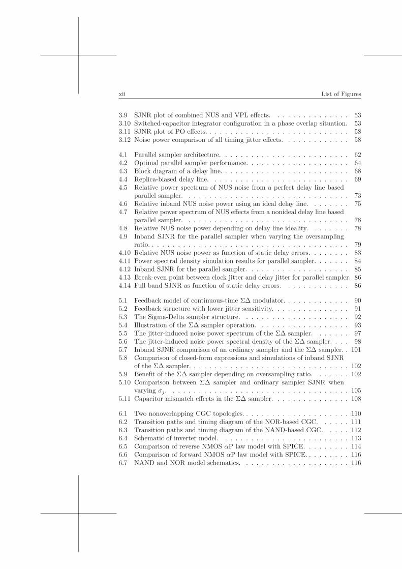
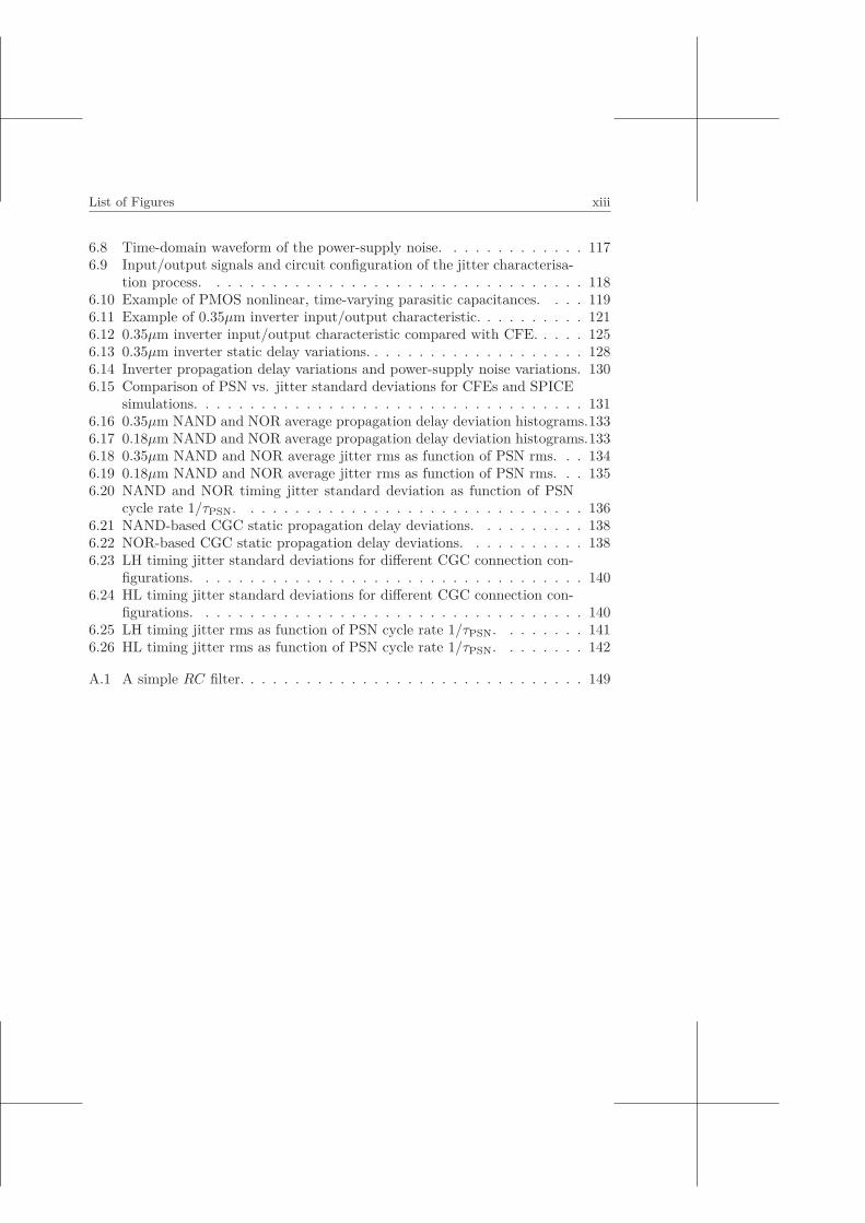
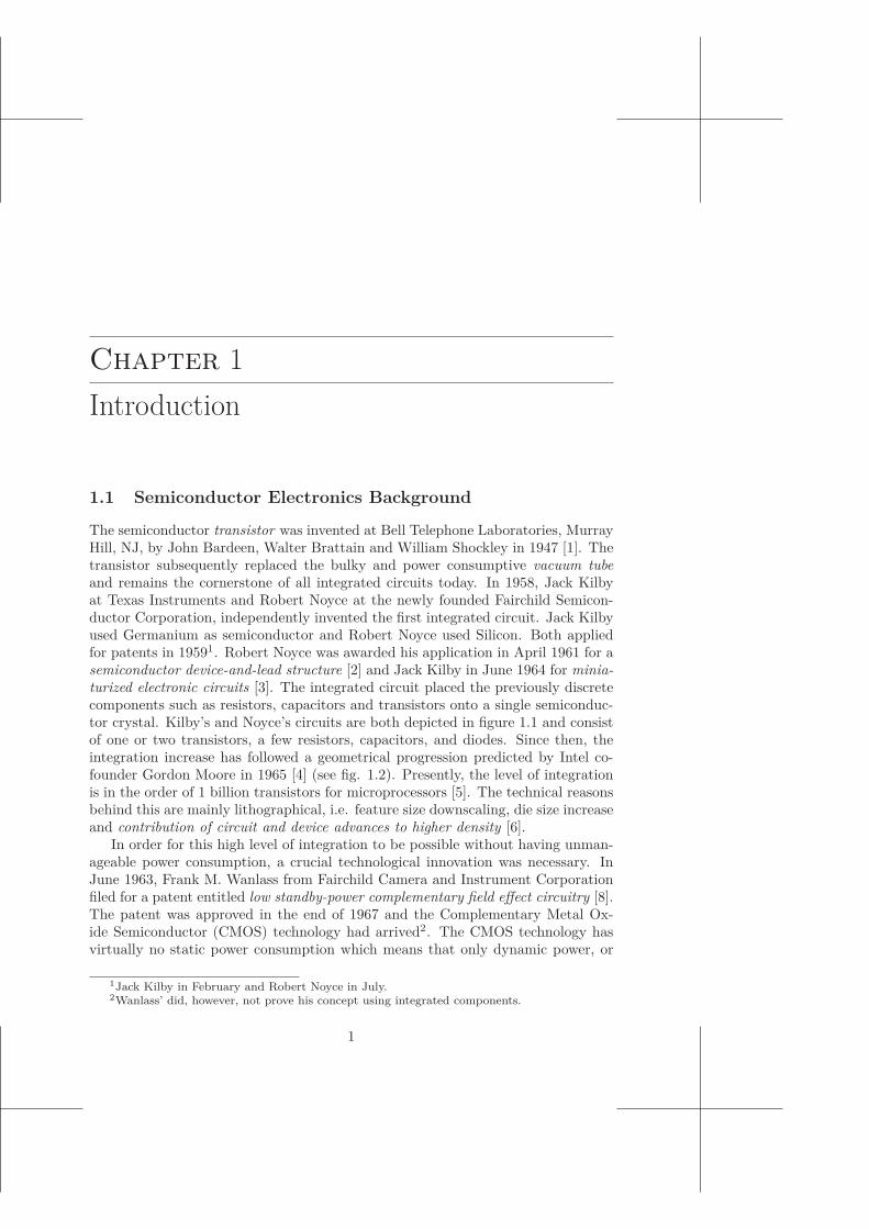
The semiconductor transistor was invented at Bell Telephone Laboratories, MurrayHill, NJ, by John Bardeen, Walter Brattain and William Shockley in 1947 [1]. Thetransistor subsequently replaced the bulky and power consumptive vacuum tubeand remains the cornerstone of all integrated circuits today. In 1958, Jack Kilbyat Texas Instruments and Robert Noyce at the newly founded Fairchild Semicon-ductor Corporation, independently invented the first integrated circuit. Jack Kilbyused Germanium as semiconductor and Robert Noyce used Silicon. Both appliedfor patents in 19591. Robert Noyce was awarded his application in April 1961 for asemiconductor device-and-lead structure [2] and Jack Kilby in June 1964 for minia-turized electronic circuits [3]. The integrated circuit placed the previously discretecomponents such as resistors, capacitors and transistors onto a single semiconduc-tor crystal. Kilby’s and Noyce’s circuits are both depicted in figure 1.1 and consistof one or two transistors, a few resistors, capacitors, and diodes. Since then, theintegration increase has followed a geometrical progression predicted by Intel co-founder Gordon Moore in 1965 [4] (see fig. 1.2). Presently, the level of integrationis in the order of 1 billion transistors for microprocessors [5]. The technical reasonsbehind this are mainly lithographical, i.e. feature size downscaling, die size increaseand contribution of circuit and device advances to higher density [6].
In order for this high level of integration to be possible without having unman-ageable power consumption, a crucial technological innovation was necessary. InJune 1963, Frank M. Wanlass from Fairchild Camera and Instrument Corporationfiled for a patent entitled low standby-power complementary field effect circuitry [8].The patent was approved in the end of 1967 and the Complementary Metal Ox-ide Semiconductor (CMOS) technology had arrived2. The CMOS technology hasvirtually no static power consumption which means that only dynamic power, or
1Jack Kilby in February and Robert Noyce in July.2Wanlass’ did, however, not prove his concept using integrated components.
1

2 CHAPTER 1. INTRODUCTION
+V
3 kΩ3 kΩ R1R2
R4 = 400 Ω
C1 = 50 μF
R8 = 1.8 kΩ
R7 = 400 ΩOutput-2
R3 = 1.8 kΩ
C2 = 50 μF
−V
Output-1
400 Ω400 Ω R5R6
GND
Input-2
Input-1
T2T1
Figure 1.1: Schematics of (left) Kilby’s [3] and (right) Noyce’s [2] integrated circuitspatented in 1964 and 1961 respectively.
2006200420022000199819961994199219901988198619841982198019781976197419721970 year
num
bero
ftra
nsist
ors
featu
resiz
e[n
m]
clock
frequ
ency
[Hz]
number of transistorsmanufacturing process feature sizeclock frequency
101
102
103
104
103
104
105
106
107
108
109
105
106
107
108
109
1010
Pentium 4
Pentium IIIPentium Pro
Pentium II
Pentium4863868028680868085808080084004
Figure 1.2: Visualizations of Moore’s law showing the evolution of Intel Microprocessors’in terms of number of transistors, clock frequency, and manufacturing process feature size[7].
1.2. BRIEF HISTORICAL REVIEW OF DATA CONVERTERS 3
switching power, is consumed. As more modern technologies were introduced andthe transistor counts reached the order of millions, the leakage currents throughthe ever thinner oxide layers increased and the tiny static power consumption be-came a more significant part of the overall power consumption. Today, static powerconsumption is at a level of 35% of total power consumption for microprocessors in90nm process technology [9].
Analog integrated circuits have not benefited to the same extent of the advancesin digital electronics integration since analog functionality is based on physical prop-erties of individual devices, such as resistance, capacitance and inductance. Theseproperties are largely decoupled from digital functionality although performancemetrics such as speed and power consumption are still governed by them. Digitalfunctionality is to a large extent independent of technology as long as the integrityand distinction of the binary representations are maintained, i.e. noise marginskept sufficiently large. However, with the performance increase of digital electron-ics and the following decrease of cost per transistor, analog design has been shiftedtowards using standard digital CMOS manufacturing technologies. The loss in per-formance by using inexpensive digital process technologies, i.e. bulk CMOS, hasbeen reclaimed through an outsourcing of functionality from the analog to the dig-ital domain and also by using clever circuit techniques and new circuit topologies[10]. However, many challenges still exist and problems mount up as the minimumfeature size continues to shrink into the nanometer range3.
1.2 Brief Historical Review of Data Converters
The first data converters had nothing to do with electronics and were conceived offar ahead of the discovery of electronic circuits. One of the first recorded digital-to-analog converter (DAC) was hydraulic and used in the 18th century in Turkey underthe Ottoman empire to meter water [11]. The advent of electronic data convertersis closely coupled with the evolution of electronic communication starting in 1753with the electric telegraph4 [12] and especially Pulse-Code Modulation (PCM) firstdescribed in a patent filed in 1921 by Paul M. Rainey [13]. Rainey’s patent includedboth an analog-to-digital converter (ADC) and a DAC which were electro-optical-mechanical. However, the patent was unfortunately forgotten until years later whenmany other PCM patents had already been issued. In 1937, Alec Harley Reeves fileda patent [14] on PCM in France5 entitled Electric Signaling System which containedone of the first electronic ADCs and DACs on record. Reeves’ converters were ofthe counting type which, for the ADC, essentially converted the analog voltageto a pulse with a width being proportional to the analog voltage. The width issubsequently digitized by counting how many clock pulses fit within the wider pulse.
3Intel will, for example, start manufacturing chips using 45nm feature size in 2007.4Even though the earliest known proposal is dated 1753, most of the development which made
the electric telegraph practical was done in the period 1825 – 1875 [12].5The first patent was filed in France but shortly after also in Britain and the U.S.
4 CHAPTER 1. INTRODUCTION
amplitude
time
analog signal
quan
tizat
ion
step
s
pulse-code modulatedrepresentation
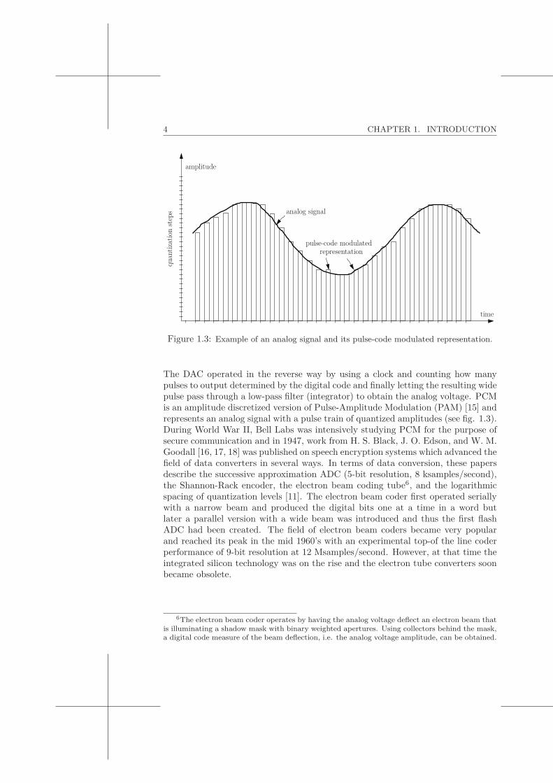
Figure 1.3: Example of an analog signal and its pulse-code modulated representation.
The DAC operated in the reverse way by using a clock and counting how manypulses to output determined by the digital code and finally letting the resulting widepulse pass through a low-pass filter (integrator) to obtain the analog voltage. PCMis an amplitude discretized version of Pulse-Amplitude Modulation (PAM) [15] andrepresents an analog signal with a pulse train of quantized amplitudes (see fig. 1.3).During World War II, Bell Labs was intensively studying PCM for the purpose ofsecure communication and in 1947, work from H. S. Black, J. O. Edson, and W. M.Goodall [16, 17, 18] was published on speech encryption systems which advanced thefield of data converters in several ways. In terms of data conversion, these papersdescribe the successive approximation ADC (5-bit resolution, 8 ksamples/second),the Shannon-Rack encoder, the electron beam coding tube6, and the logarithmicspacing of quantization levels [11]. The electron beam coder first operated seriallywith a narrow beam and produced the digital bits one at a time in a word butlater a parallel version with a wide beam was introduced and thus the first flashADC had been created. The field of electron beam coders became very popularand reached its peak in the mid 1960’s with an experimental top-of the line coderperformance of 9-bit resolution at 12 Msamples/second. However, at that time theintegrated silicon technology was on the rise and the electron tube converters soonbecame obsolete.
6The electron beam coder operates by having the analog voltage deflect an electron beam thatis illuminating a shadow mask with binary weighted apertures. Using collectors behind the mask,a digital code measure of the beam deflection, i.e. the analog voltage amplitude, can be obtained.
1.2. BRIEF HISTORICAL REVIEW OF DATA CONVERTERS 5
(b)
quantized outputwith single step
of error compensationfor transmission
subtractor
quantizer
delay
addersampler
sourcetiming
input signal
(a)
Signal amplifier
circuitAmplitude comparison
voltage generatorLocal comparison
Phase inverterPulse generator
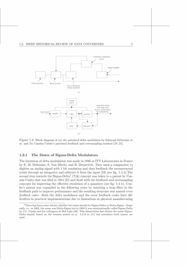
Figure 1.4: Block diagram of (a) the patented delta modulator by Edmond Deloraine etal. and (b) Cassius Cutler’s patented feedback and oversampling method [19, 21].
1.2.1 The Dawn of Sigma-Delta ModulatorsThe invention of delta modulation was made in 1946 at ITT Laboratories in Franceby E. M. Deloraine, S. Van Mierlo, and B. Derjavitch. They used a comparator todigitize an analog signal with 1 bit resolution and then feedback the reconstructedresult through an integrator and subtract it from the input [19] (see fig. 1.4 a).Thesecond step towards the Sigma-Delta7 (ΣΔ) concept was taken in a patent by Cas-sius Cutler that was filed in 1954 [21] and dealt with the feedback and oversamplingconcepts for improving the effective resolution of a quantizer (see fig. 1.4 b). Cut-ler’s patent was expanded in the following years by inserting a loop filter in thefeedback path to improve performance and the resulting structure was named errorfeedback coder. Both the delta modulator and the error feedback coder have dif-ficulties in practical implementations due to limitations in physical manufacturing
7There has been some debate whether the name should be Sigma-Delta or Delta-Sigma. Origi-nally, i.e. in 1962, the name was Delta-Sigma but in 1963 it was unintentionally called Sigma-Deltaby J.C. Candy and his colleagues at Bell Labs [20]. This dissertation has chosen the name Sigma-Delta mainly based on the reasons stated on p. 3.113 in [11] but nowadays both names areused.
6 CHAPTER 1. INTRODUCTION
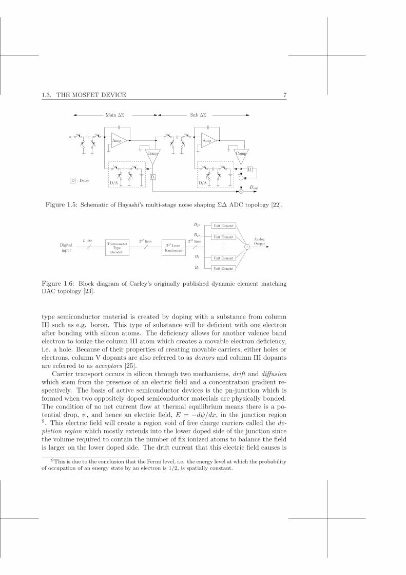
accuracy and the need of an equalizer at the receiver end. In 1962, three Japaneseresearchers, Inose, Yasuda, and Marakami, proposed an architecture named Delta-Sigma modulator which consisted of a subtracter (Δ), a loop filter, which in thesimple case was an integrator (Σ), followed by a quantizer and a 1-bit DAC in thefeedback path. The main advantage of the ΣΔ modulator compared to the deltamodulator is that the quantization noise is high-pass shaped while the signal isn’taffected. Furthermore, the feedback path is easy to realize accurately if a 1-bitDAC is used so the drawback of the error feedback coder is also overcome. Thenext important advancement in ΣΔ ADCs was in 1977 when Ritchie in his Ph.D.thesis proposed to use several integrators in the feedforward path, each with a feed-back component from the DAC. However, using more than two integrators in thefeedforward path gave stability concerns which had to be simulated numerically.Later on, higher order structures such as fourth and fifth order ΣΔ ADCs havebeen designed with the help of the design techniques presented in 1987 by Lee inhis M.Sc. thesis and by Chao et al. in his paper from 1990 “A higher order topologyfor interpolative modulators for oversampling A/D conversion”. However, in 1986a novel technique for designing higher order modulators with inherent stability waspresented by Hayashi et al. [22] named the MASH (Multi-stAge noiSe sHaping)where two or more lower order ΣΔ structures are cascaded after each other andwhere the following stages only process the quantization noise of the previous stage(see fig. 1.5). The main drawback of MASH structures is the necessity of match-ing analog and digital transfer functions for successful cancellation of lower ordershaped quantization noise. Yet another way of improving the ΣΔ ADC perfor-mance is to increase the quantizer and DAC resolutions but since any nonidealitiesin the DAC show up directly at the output this wasn’t a practical way to go untilCarley in 1989 [23] presented the use of dynamic element matching to reduce theeffects of DAC nonlinearity (see fig. 1.6).
As a sample of the evolution of analog-to-digital converters in recent years, thebandwidth (speed) of integrated flash analog-to-digital converters has evolved withbenefit from Moore’s law at an exponential rate [24] with roughly a factor of tenperformance increase every five years since 1997. However, the improvement inconversion power consumption efficiency hasn’t improved at the same rate, witha tenfold improvement in nine years. In 2002, this was more than five orders ofmagnitude higher than the theoretical8 efficiency limit [24].
1.3 The MOSFET device
An N-type semiconductor material is created by doping e.g. silicon with a substancehaving five valence electrons, i.e. from column V in the periodic table, such asarsenic or phosphorus. These substances will have the fifth electron loosely bondedafter having formed covalent bonds with other silicon atoms. Conversely, a P-
8This theoretical limit does not take active circuitry power consumption into account. It onlyconsiders thermal noise. See appendix A for a deduction of the theoretical limit.
1.3. THE MOSFET DEVICE 7
+
+ −+
Dout
D
Comp
Amp
D/AD
D/A: Delay
Comp
Amp
Sub ΔΣMain ΔΣ
D
Figure 1.5: Schematic of Hayashi’s multi-stage noise shaping ΣΔ ADC topology [22].
B2M
B2M−1
B1
B0
2M lines AnalogOutput
+
Unit Element
Unit Element
...
Unit Element
Unit Element
2M LinesRandomizer
2M linesThermometer
TypeDecoder
L bits
inputDigital
Figure 1.6: Block diagram of Carley’s originally published dynamic element matchingDAC topology [23].
type semiconductor material is created by doping with a substance from columnIII such as e.g. boron. This type of substance will be deficient with one electronafter bonding with silicon atoms. The deficiency allows for another valence bandelectron to ionize the column III atom which creates a movable electron deficiency,i.e. a hole. Because of their properties of creating movable carriers, either holes orelectrons, column V dopants are also referred to as donors and column III dopantsare referred to as acceptors [25].
Carrier transport occurs in silicon through two mechanisms, drift and diffusionwhich stem from the presence of an electric field and a concentration gradient re-spectively. The basis of active semiconductor devices is the pn-junction which isformed when two oppositely doped semiconductor materials are physically bonded.The condition of no net current flow at thermal equilibrium means there is a po-tential drop, ψ, and hence an electric field, E = −dψ/dx, in the junction region9. This electric field will create a region void of free charge carriers called the de-pletion region which mostly extends into the lower doped side of the junction sincethe volume required to contain the number of fix ionized atoms to balance the fieldis larger on the lower doped side. The drift current that this electric field causes is
9This is due to the conclusion that the Fermi level, i.e. the energy level at which the probabilityof occupation of an energy state by an electron is 1/2, is spatially constant.
8 CHAPTER 1. INTRODUCTION
BulkGate
Source
Drain
Bulk
Source
GateDrain
SourceGateDrain
Bulk
SourceGateDrain metal
PMOSNMOS
channeln-well
p+p+
pp
n+n+
channel Si
SiO2
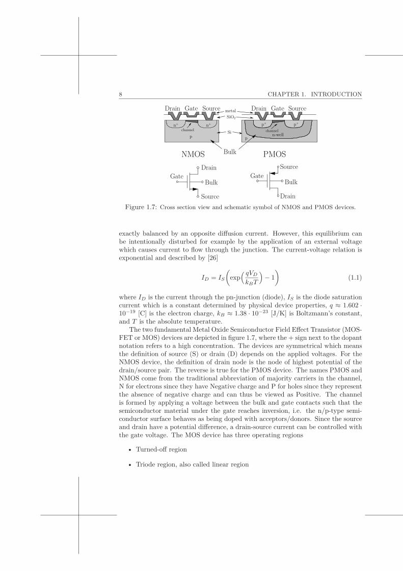
Figure 1.7: Cross section view and schematic symbol of NMOS and PMOS devices.
exactly balanced by an opposite diffusion current. However, this equilibrium canbe intentionally disturbed for example by the application of an external voltagewhich causes current to flow through the junction. The current-voltage relation isexponential and described by [26]
ID = IS
(exp
( qVD
kBT
)− 1
)(1.1)
where ID is the current through the pn-junction (diode), IS is the diode saturationcurrent which is a constant determined by physical device properties, q ≈ 1.602 ·10−19 [C] is the electron charge, kB ≈ 1.38 · 10−23 [J/K] is Boltzmann’s constant,and T is the absolute temperature.
The two fundamental Metal Oxide Semiconductor Field Effect Transistor (MOS-FET or MOS) devices are depicted in figure 1.7, where the + sign next to the dopantnotation refers to a high concentration. The devices are symmetrical which meansthe definition of source (S) or drain (D) depends on the applied voltages. For theNMOS device, the definition of drain node is the node of highest potential of thedrain/source pair. The reverse is true for the PMOS device. The names PMOS andNMOS come from the traditional abbreviation of majority carriers in the channel,N for electrons since they have Negative charge and P for holes since they representthe absence of negative charge and can thus be viewed as Positive. The channelis formed by applying a voltage between the bulk and gate contacts such that thesemiconductor material under the gate reaches inversion, i.e. the n/p-type semi-conductor surface behaves as being doped with acceptors/donors. Since the sourceand drain have a potential difference, a drain-source current can be controlled withthe gate voltage. The MOS device has three operating regions
• Turned-off region
• Triode region, also called linear region
1.3. THE MOSFET DEVICE 9
VGSn = 3.3 VVGSn = 3 V
VGSn = 2.5 V
VGSn = 2 V
VGSn = 1.5 V
VGSn = 1 V
VSGp = 3.3 V
VSGp = 3 V
VSGp = 2.5 V
VSGp = 2 VVSGp = 1.5 V
VSGp = 1 V
saturation region
triode region
saturation regiontriode region
NMOS
PMOS
VDS [V]
I DS
[mA
]
-4 -3 -2 -1 0 1 2 3 4-6
-4
-2
0
2
4
6
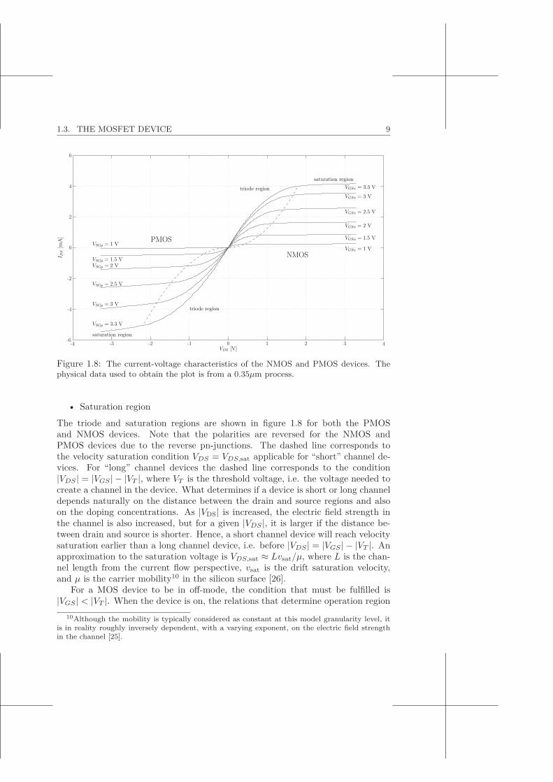
Figure 1.8: The current-voltage characteristics of the NMOS and PMOS devices. Thephysical data used to obtain the plot is from a 0.35μm process.
• Saturation region
The triode and saturation regions are shown in figure 1.8 for both the PMOSand NMOS devices. Note that the polarities are reversed for the NMOS andPMOS devices due to the reverse pn-junctions. The dashed line corresponds tothe velocity saturation condition VDS = VDS,sat applicable for “short” channel de-vices. For “long” channel devices the dashed line corresponds to the condition|VDS | = |VGS | − |VT |, where VT is the threshold voltage, i.e. the voltage needed tocreate a channel in the device. What determines if a device is short or long channeldepends naturally on the distance between the drain and source regions and alsoon the doping concentrations. As |VDS| is increased, the electric field strength inthe channel is also increased, but for a given |VDS |, it is larger if the distance be-tween drain and source is shorter. Hence, a short channel device will reach velocitysaturation earlier than a long channel device, i.e. before |VDS | = |VGS | − |VT |. Anapproximation to the saturation voltage is VDS,sat ≈ Lvsat/μ, where L is the chan-nel length from the current flow perspective, vsat is the drift saturation velocity,and μ is the carrier mobility10 in the silicon surface [26].
For a MOS device to be in off-mode, the condition that must be fulfilled is|VGS | < |VT |. When the device is on, the relations that determine operation region
10Although the mobility is typically considered as constant at this model granularity level, itis in reality roughly inversely dependent, with a varying exponent, on the electric field strengthin the channel [25].
10 CHAPTER 1. INTRODUCTION
are
Triode: |VDS | < |VDS,sat|, IDS = ±μCoxW
L
((VGS − VT )VDS − V 2
DS/2)
(1.2)
Saturation: |VDS | ≥ |VDS,sat|, IDS = ±μCoxW
2L(VGS − VT )2(1 + λVDS) (1.3)
where the negative sign is for PMOS devices and the positive is for NMOS devices.Cox is the gate capacitance per unit area, W is the width of the channel seenfrom the current flow perspective, and λ is the channel length modulation. λ isgiven by empirical data and is also inversely proportional to the channel length andaccounts for the fact that the current does increase slightly when |VDS | increasesbeyond the point of saturation. The above relations are useful for hand calculationsand approximations, but for more detailed analyses, SPICE models of differentgranularity have been developed that are suitable for computer based simulations.
The previous relations are useful for low frequencies, but at higher frequenciesparasitic capacitors between the different device terminals dominate the transistorbehavior. IC foundries typically provide device models for higher frequency behav-ior to be used by a SPICE based simulator, e.g. Spectre. There are closed formexpressions relating the parasitic capacitances to geometrical and physical proper-ties of the device but these are only useful on a larger granularity level since allparasitic capacitors are nonlinear functions of terminal voltages. Hence, computerbased simulation is the preferred choice when an accurate behavior is required.
1.4 Timing Jitter or Phase Noise
Timing Jitter or Phase Noise are two names of an uncertainty in the time instantof an event. The term timing jitter is typically used when describing phase fluc-tuations of a digital time reference whereas phase noise is used for denoting phasefluctuations of an analog time reference. Timing jitter is measured usually as eithera peak-to-peak value or an rms value (standard deviation) in seconds whereas phasenoise is measured in frequency-domain typically on a relative logarithmic densityscale at a certain frequency offset from a carrier [dBc/Hz]. A common measure ofphase noise is the single sideband noise spectral density which is a decent approxi-mation of phase noise given that amplitude noise is negligible, which is usually thecase [27].
L{Δf} = 10 log(Psideband(fc + Δf, 1 Hz)
Pcarrier
)(1.4)
Psideband is the noise power situated on the sides at a certain distance, Δf , from thecarrier frequency, fc, in a 1 Hz bandwidth and Pcarrier is the carrier signal power.
The name phase was originally used for describing the occurrence of celestialevents such as the different parts of the moon cycle [28] which were all periodic.Likewise, the modern term phase, φ(t), is defined only for periodic events and can be
1.4. TIMING JITTER OR PHASE NOISE 11
exemplified by considering the case of an ideal sinusoid, representative of a carriersignal.
Vsignal(t) = A(t) sin(φ(t)
)(1.5)
A(t) represents the possibly time variant amplitude of the signal and φ(t) is thephase growing monotonically with time according to the present time, t, dividedby the period time, Tc = 1/fc, normalized to 2π.
φ(t) = φ(0) + 2πt/Tc = φ(0) + 2πfct (1.6)
Since all periodic functions, g(t), that are bounded and piece-wise differentiablehave a Fourier Series representation [29], the above definition of phase can be ex-tended to all periodic functions.
g(t) =a0
2+
∞∑k=1
(ak cos(2πfckt) + bk sin(2πfckt)
)(1.7)
where ak and bk are given by
ak =2Tc
∫ x+Tc
x
g(t) cos(2πfckt)dt for k ≥ 0 (1.8)
bk =2Tc
∫ x+Tc
x
g(t) sin(2πfckt)dt for k ≥ 1 (1.9)
and x is any constant such that g(t) is defined over the interval [x, x + Tc]. Theintuitive interpretation is that the phase of a signal at a particular time instantrepresents a measure of how far the signal has come to reach a full cycle in itsperiod. From eq. (1.6), the relationship between frequency and phase is obtainedf = dφ/dt which is why phase noise, δφ(t), also represents a frequency uncertainty,δfc = d/dt{δφ(t)}, i.e. a spreading in the frequency spectrum around a carrier.
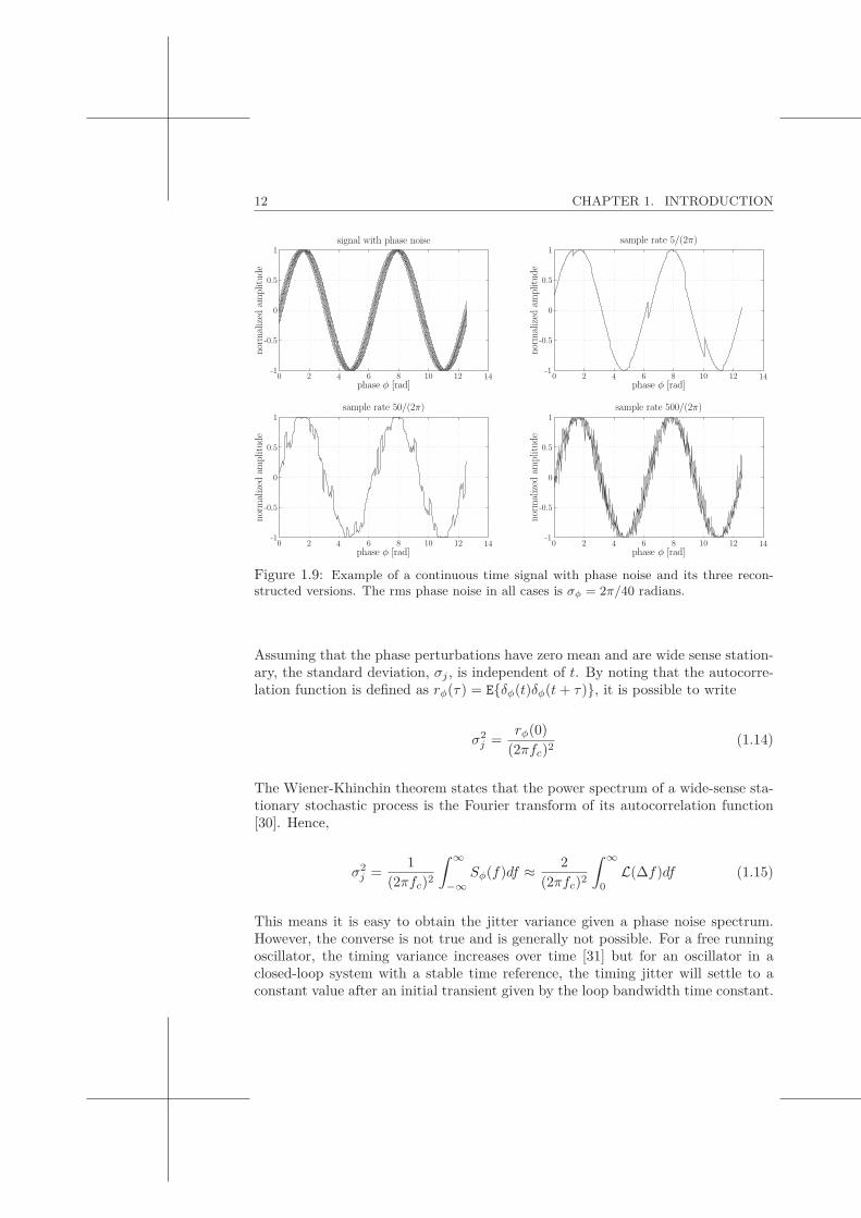
The relation between the measures of phase noise, L{Δf}, and timing jitter,σj , can be obtained by adding a phase perturbation, δφ(t), to the signal in eq. (1.5)(see fig. 1.9).
Vsignal(t) = A(t) sin(φ(t) + δφ(t)
)(1.10)
The phase perturbation can be expressed as a time deviation.
δφ(t) = 2πfcδt(t) (1.11)
This means that the perturbed signal becomes
Vsignal(t) = A(t) sin(2πfc(t+ δt(t))
)(1.12)
Taking the variance, V{·}, of the phase perturbations gives the rms jitter, σj .
σ2j = V{δt(t)} = V
{δφ(t)2πfc
}=
1(2πfc)2
(E{δ2φ(t)
}− E2{δφ(t)
})(1.13)
12 CHAPTER 1. INTRODUCTION
phase φ [rad]
norm
alize
dam
plitu
de
signal with phase noise
phase φ [rad]
norm
alize
dam
plitu
de
sample rate 5/(2π)
phase φ [rad]
norm
alize
dam
plitu
de
sample rate 50/(2π)
phase φ [rad]
norm
alize
dam
plitu
de
sample rate 500/(2π)
0 2 4 6 8 10 12 140 2 4 6 8 10 12 14
0 2 4 6 8 10 12 140 2 4 6 8 10 12 14
-1
-0.5
0
0.5
1
-1
-0.5
0
0.5
1
-1
-0.5
0
0.5
1
-1
-0.5
0
0.5
1
Figure 1.9: Example of a continuous time signal with phase noise and its three recon-structed versions. The rms phase noise in all cases is σφ = 2π/40 radians.
Assuming that the phase perturbations have zero mean and are wide sense station-ary, the standard deviation, σj , is independent of t. By noting that the autocorre-lation function is defined as rφ(τ) = E{δφ(t)δφ(t+ τ)}, it is possible to write
σ2j =
rφ(0)(2πfc)2
(1.14)
The Wiener-Khinchin theorem states that the power spectrum of a wide-sense sta-tionary stochastic process is the Fourier transform of its autocorrelation function[30]. Hence,
σ2j =
1(2πfc)2
∫ ∞
−∞Sφ(f)df ≈ 2
(2πfc)2
∫ ∞
0
L(Δf)df (1.15)
This means it is easy to obtain the jitter variance given a phase noise spectrum.However, the converse is not true and is generally not possible. For a free runningoscillator, the timing variance increases over time [31] but for an oscillator in aclosed-loop system with a stable time reference, the timing jitter will settle to aconstant value after an initial transient given by the loop bandwidth time constant.
1.5. MOTIVATION OF THIS WORK 13
1.5 Motivation of this work
This dissertation deals with timing uncertainty in Sigma-Delta (ΣΔ) Analog-to-Digital Converters. The time reference, or clock, in any ADC usually originatesfrom a crystal oscillator either on-chip or off-chip. A crystal oscillator has a veryhigh frequency accuracy but is not flexible in terms of frequency selection. Typicalphase noise figures, for a temperature compensated crystal oscillator frequency of20 MHz, is -54 dBc/Hz @ 1 Hz carrier distance, -86 dBc/Hz @ 10 Hz distance,-135 dBc/Hz @ 1 kHz distance and -151 dBc/Hz @ 100 kHz distance. For anoven (temperature) controlled crystal oscillator, popular in telecommunications,satellite, and broadcast applications, the performance is even higher, starting from-130 dBc/Hz @ 10 Hz distance and going down to -160 dBc/Hz @ 50 kHz distancefor an oscillation frequency of 10 MHz [32]. However, these oscillators have a powerdissipation of a few watts which makes them unsuitable for mobile applications.
Due to the crystal oscillator frequency inflexibility, a phase-locked loop (PLL)is usually used to upconvert the crystal oscillator signal to a desired frequency.Inherent electronic noise such as thermal, shot, and flicker noise combined withpower-supply noise and substrate noise reduce the phase noise performance of thetiming reference that is created. Generally, if the output frequency of a PLL isincreased by increasing the division ratio in the PLL feedback loop, the phase noiseor timing jitter also increases [27, 33, 34]. Hence, as technology advances andhigher ADC speeds become possible there are difficulties that arise which were notdominant at lower frequencies. This is true for any ADC architecture but is mostsignificant in types of ADCs that are on the high-end limit of the resolution rangesuch as ΣΔ ADCs. This is because the ΣΔ architecture has an operation principlewhich trades speed for resolution, i.e. the higher the oversampling ratio the higherthe resolution becomes.
Technology advancement per se is not driving the need for faster ADCs butonly facilitates it. The driving force is the desire of creating a flexible communi-cations system, i.e. a system being able to handle many different communicationsstandards, e.g. GSM, Bluetooth, WLAN, WiMAX, etc. This means being ableto handle many different carrier frequencies and bandwidths, and the conceptuallymost attractive solution would be to convert the RF signal directly to digital andthen process the signal content digitally. This utopia is what has been dubbedSoftware Radio and means a full level of reconfigurability at the software level, i.e.by programming the communications system [35]. There are many obstacles to beovercome before Software Radio can become a reality and they are primarily relatedto the ADC which is to act as RF interface. One of the critical ADC issues thatneeds to be solved, except power consumption, is how to achieve sufficient accuracyat such a high frequency (several GHz). One of the obstacles in obtaining a highaccuracy is how to operate with a nonideal time reference without losing too muchin performance. This has been the fundamental question behind this dissertation.
14 CHAPTER 1. INTRODUCTION
1.6 Thesis Outline
The work presented in this thesis aims at describing, modelling, and improving thetiming uncertainty performance limitations of Analog-to-Digital Converters withspecial focus on switched-capacitor Sigma-Delta modulators.
This dissertation is organized into seven chapters. The outline of each chapteris as follows:
Chapter 1 gives an introduction and background structure to this work, moti-vates the importance of this thesis and describes the thesis outline and the author’scontributions.
Chapter 2 introduces the concept of Analog-to-Digital Conversion and motivatesthe need of conversion together with a brief historical review of the evolution ofADCs. Moreover, this chapter gives several examples of converter architecturestogether with pros and cons. Finally, the general characteristics of Sigma-Deltamodulation and noise shaping are explained.
Chapter 3 presents three effects of timing uncertainty in switched-capacitorSigma-Delta Analog-to-Digital Converters. Each effect is analyzed and the im-pact is modelled and predicted through the development of accurate closed-formmathematical expressions. The predictions are validated through simulations anda comparison is made between the effects in order to focus the attention on thedominant effect. The chapter is based on publications [2] and [6] of the author.
Chapter 4 introduces the parallel sampler architecture which has been inventedby the author to improve the jitter performance limitation mainly of switched-capacitor Sigma-Delta modulators but the principle can be extended to other con-verter architectures. An analysis of the parallel sampler topology follows wherethe principle of operation is explained together with examples of circuit nonideal-ity effects. Moreover, a clock generation structure is suggested for supplying theparallel sampler with necessary time references. The performance of the parallelsampler is accurately modelled through mathematical closed-form expressions thatare verified through simulations. The chapter is based on publications [1] and [3]of the author.
Chapter 5 describes the Sigma-Delta sampler topology which has been inventedby the author primarily to decrease the jitter sensitivity of switched-capacitorSigma-Delta modulators but the idea can be expanded to boost the performanceof other converter architectures. The principle behind the Sigma-Delta sampleroperation is explained and the performance enhancements that are obtainable arethoroughly explored. Furthermore, mismatch effects are investigated and deter-mined to have a negligible effect on the overall sampler performance. Closed-form
1.7. AUTHOR’S CONTRIBUTIONS 15
mathematical expressions predicting the performance and limitations of the Sigma-Delta sampler are given and verified with simulations. The chapter is based onpublication [4] of the author.
Chapter 6 gives an analysis of the effects of power-supply and substrate noisein nonoverlapping clock generation circuits that are commonly used in switched-capacitor ΣΔ ADCs. Two nonoverlapping clock generation circuits are brokendown into constituent parts where each part is analyzed and characterized sepa-rately. Closed-form mathematical expressions that accurately describe the power-supply noise induced jitter properties of the inverter block are presented and verifiedthrough simulations. It is also shown that the other logical blocks have character-istics that are very similar to the inverter’s. Finally, all constituent blocks are con-nected to form the clock generation circuits and a system level analysis is performedthat qualitatively explains the overall performance obtained through simulations.The chapter is based on publications [7-10] of the author.
Chapter 7 concludes the dissertation.
1.7 Author’s Contributions
This thesis is based on the publications given in the publication list. The contentof the publications are as follows:
In [1], the author introduces and analyzes the parallel sampler architecture. Fur-thermore, closed-form mathematical expressions of the jitter suppression perfor-mance are given and verified through simulations of a fourth order 2-2 MASH ΣΔmodulator. This work is largely covered in chapter 4 in this dissertation.
In [2], the author presents the effects of timing uncertainty in a switched-capacitorSigma-Delta ADC. Three effects are distinguished, analyzed and quantified in termsof induced noise power. Closed-form expressions are developed and verified withsimulations performed on a fourth order 2-2 MASH ΣΔ ADC. This work is partlycovered in chapter 3 in this dissertation.
In [3], the author further explores the parallel sampler architecture through theanalysis of deteriorating effects from the delay line and also from capacitor mismatcheffects. Moreover, a frequency-domain treatment is made concluding that whitefrequency timing jitter transforms into colored amplitude noise as the number ofdelay elements in the delay line grows. Closed-form mathematical expressions aregiven that predict the parallel sampler performance in conjunction with a delay linethat has delay jitter and static delay errors. The accuracy of the results are verifiedthrough simulations. This publication is covered in chapter 4 in this dissertation.

16 CHAPTER 1. INTRODUCTION
In [4], the author introduces and analyzes the Sigma-Delta sampler architecture.The sampler’s principle of operation is explained and mismatch effects are exploredand determined to be of minor importance. Mathematical closed-form expressionsare given that accurately predict the Sigma-Delta sampler’s jitter suppression per-formance, both spectrally and in terms of SJNR. The accuracy of the closed-formexpressions and mathematical mismatch results are verified with simulations. Thispublication is covered in chapter 5 in this dissertation.
In [5], the author has contributed with a mathematical treatment of jitter accumu-lation effects in the analysis of a frequency detector for a wireless LAN frequencysynthesizer. It was determined that the jitter impact of the frequency detectoris reduced as the operation of the detector creates an average of the individualjitter contributors of the time reference. This publication is not covered in thisdissertation.
In [6], the author expands on the analysis performed in [2] to include SJNR metricsand an exploration of simultaneous impact of two of the effects is investigated.Closed-form mathematical expressions that accurately describe the impact of eachjitter-induced effect are given. The accuracy of the closed-form expressions areverified with simulations on a second order, single-stage ΣΔ modulator. Finally, acomparison of the three effects is made to determine if one effect dominates overthe other two. This publication is covered in chapter 3 in this dissertation.
In [7], the author presents an analysis of the transformation process from power-supply and substrate noise to timing jitter in inverters. A detailed transistor levelmathematical treatment is performed that results in accurate closed-form expres-sions. The expressions predict the input/output characteristic, static propagationdelay variations and also the induced jitter rms values based on voltage variationsin the power-supply network. The accuracy of the given closed-form expressions isthoroughly verified through simulations in Cadence. This publication is covered inchapter 6 in this dissertation.
In [8], the author extends the analysis in [7] to encompass NAND and NOR logicblocks. It is determined that a mathematical treatment is not possible as the bound-aries between different operating regions are dependent on the power-supply noiseand cannot be accurately approximated with deterministic quantities. Propagationdelay variations are obtained through co-simulations of MATLAB and Cadence andthe NAND and NOR blocks are determined to have jitter characteristics similar tothe inverter. This publication is covered in chapter 6 in this dissertation.
In [9], the author presents an investigation of two nonoverlapping clock generationcircuits which comprise of the logic blocks described in [7] and [8]. Cadence sim-ulations in conjunction with MATLAB data analysis are performed and a systemlevel analysis explaining the power-supply noise sensitivity of both clock genera-tion circuits is included. Different connection configurations of the clock generation
1.7. AUTHOR’S CONTRIBUTIONS 17
circuits are also explored and compared in terms of jitter performance and suscep-tibility to power-supply noise. Finally, a frequency sensitivity analysis is presented.This publication is covered in chapter 6 in this dissertation.
In [10], the author expands on the analyses done in [7-9] including more detailedcomparison of the two nonoverlapping clock generation circuits, both in time-domain and frequency-domain. It is concluded that constructive interference ofpower-supply noise induced timing jitter is important to avoid. One way of achiev-ing this is to make the propagation delays of the constituent logic blocks different.This publication is covered in chapter 6 in this dissertation.


Chapter 2Analog-to-Digital Conversion
2.1 Principles of Conversion between Analog and Digital
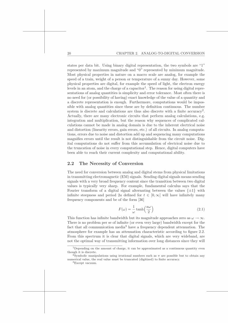
An analog quantity is defined as a quantity which can take on a continuum of valueswhereas a digital quantity can only take on a discrete and finite set of values. Analogalso refers to continuous in time whereas digital corresponds to discrete values atdiscrete points in time (see fig. 2.1). Conceptually, digitizing an analog quantity isa mapping procedure between fixed time and magnitude points and the continuousanalog quantity. Of course, if the digital quantity is to provide a fair representationof its analog version there are several criteria for granularity both in magnitude(quantizer resolution) and time (sampling frequency).
Usually, a digital quantity is represented in a binary way with only two discrete
time
magnitude
analog quantity digital quantity
Figure 2.1: Visualization of relation between analog and digital quantities.
19
20 CHAPTER 2. ANALOG-TO-DIGITAL CONVERSION
states per data bit. Using binary digital representation, the two symbols are “1”represented by maximum magnitude and “0” represented by minimum magnitude.Most physical properties in nature on a macro scale are analog, for example thespeed of a train, weight of a person or temperature of a sunny day. However, somephysical properties are digital, for example the speed of light, the electron energylevels in an atom, and the charge of a capacitor1. The reason for using digital repre-sentations of analog quantities is simplicity and error tolerance. Most often there isno need for (or possibility of having) exact knowledge of the value of a quantity anda discrete representation is enough. Furthermore, computations would be impos-sible with analog quantities since these are by definition continuous. The numbersystem is discrete and calculations are thus also discrete with a finite accuracy2.Actually, there are many electronic circuits that perform analog calculations, e.g.integration and multiplication, but the reason why sequences of complicated cal-culations cannot be made in analog domain is due to the inherent electrical noiseand distortion (linearity errors, gain errors, etc.) of all circuits. In analog computa-tions, errors due to noise and distortion add up and sequencing many computationsmagnifies errors until the result is not distinguishable from the circuit noise. Dig-ital computations do not suffer from this accumulation of electrical noise due tothe truncation of noise in every computational step. Hence, digital computers havebeen able to reach their current complexity and computational ability.
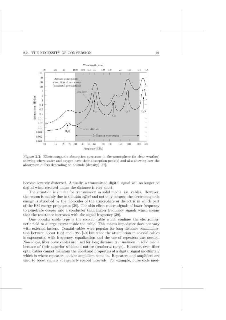
2.2 The Necessity of Conversion
The need for conversion between analog and digital stems from physical limitationsin transmitting electromagnetic (EM) signals. Sending digital signals means sendingsignals with a very broad frequency content since the transition between two digitalvalues is typically very sharp. For example, fundamental calculus says that theFourier transform of a digital signal alternating between the values {±1} withinfinite steepness and period 2a defined for t ∈ [0,∞] will have infinitely manyfrequency components and be of the form [36]
F (ω) =1ω
tanh(aω
2
)(2.1)
This function has infinite bandwidth but its magnitude approaches zero as ω → ∞.There is no problem per se of infinite (or even very large) bandwidth except for thefact that all communication media3 have a frequency dependent attenuation. Theatmosphere for example has an attenuation characteristic according to figure 2.2.From this spectrum it is clear that digital signals, which are very wideband, arenot the optimal way of transmitting information over long distances since they will
1Depending on the amount of charge, it can be approximated as a continuous quantity eventhough it is discrete.
2Symbolic manipulations using irrational numbers such as π are possible but to obtain anynumerical value, the real value must be truncated (digitized) to finite accuracy.
3Except vacuum.
2.2. THE NECESSITY OF CONVERSION 21
absorption of mm wavesAverage atmospheric
(horizontal propagation)
O2
Wavelength [mm]0.81.01.52.03.04.05.06.08.010.0152030
Millimeter wave region
4 km altitude
H2OH2O
H2O
O2
Sea level
0.0010.0020.004
0.010.020.04
0.10.20.4
12
4102040
100
Atte
nuat
ion
[dB/
km]
Frequency [GHz]4003002001501008060504030252010 15
Figure 2.2: Electromagnetic absorption spectrum in the atmosphere (in clear weather)showing where water and oxygen have their absorption peak(s) and also showing how theabsorption differs depending on altitude (density) [37].
become severely distorted. Actually, a transmitted digital signal will no longer bedigital when received unless the distance is very short.
The situation is similar for transmission in solid media, i.e. cables. However,the reason is mainly due to the skin effect and not only because the electromagneticenergy is absorbed by the molecules of the atmosphere or dielectric in which partof the EM energy propagates [38]. The skin effect causes signals of lower frequencyto penetrate deeper into a conductor than higher frequency signals which meansthat the resistance increases with the signal frequency [39].
One popular cable type is the coaxial cable which confines the electromag-netic field to a large extent inside the cable. This means impedance does not varywith external factors. Coaxial cables were popular for long distance communica-tion between about 1953 and 1986 [40] but since the attenuation in coaxial cablesis exponential with frequency, equalization and the use of repeaters was needed.Nowadays, fiber optic cables are used for long distance transmission in solid mediabecause of their superior wideband nature (terahertz range). However, even fiberoptic cables cannot maintain the wideband properties of a digital signal indefinitelywhich is where repeaters and/or amplifiers come in. Repeaters and amplifiers areused to boost signals at regularly spaced intervals. For example, pulse code mod-
22 CHAPTER 2. ANALOG-TO-DIGITAL CONVERSION
digital
analogVLSB
LSB
Figure 2.3: General representation of ideal bipolar analog to digital transfer function.
ulated electrical telephone signals through copper cable pairs in the United Statesuse repeaters every 1.8 km [11]. Fiber optic cables need repeaters approximatelyevery 100 km depending on cable type [40].
Because of the frequency dependent attenuation of transmission media and alsoto use the limited frequency spectrum more efficiently, the typical approach forlong distance communication is to use “narrowband” signals, which by definitionare analog. Hence, when transmitting digital data and receiving analog signals4,there is a need for conversion between analog and digital.
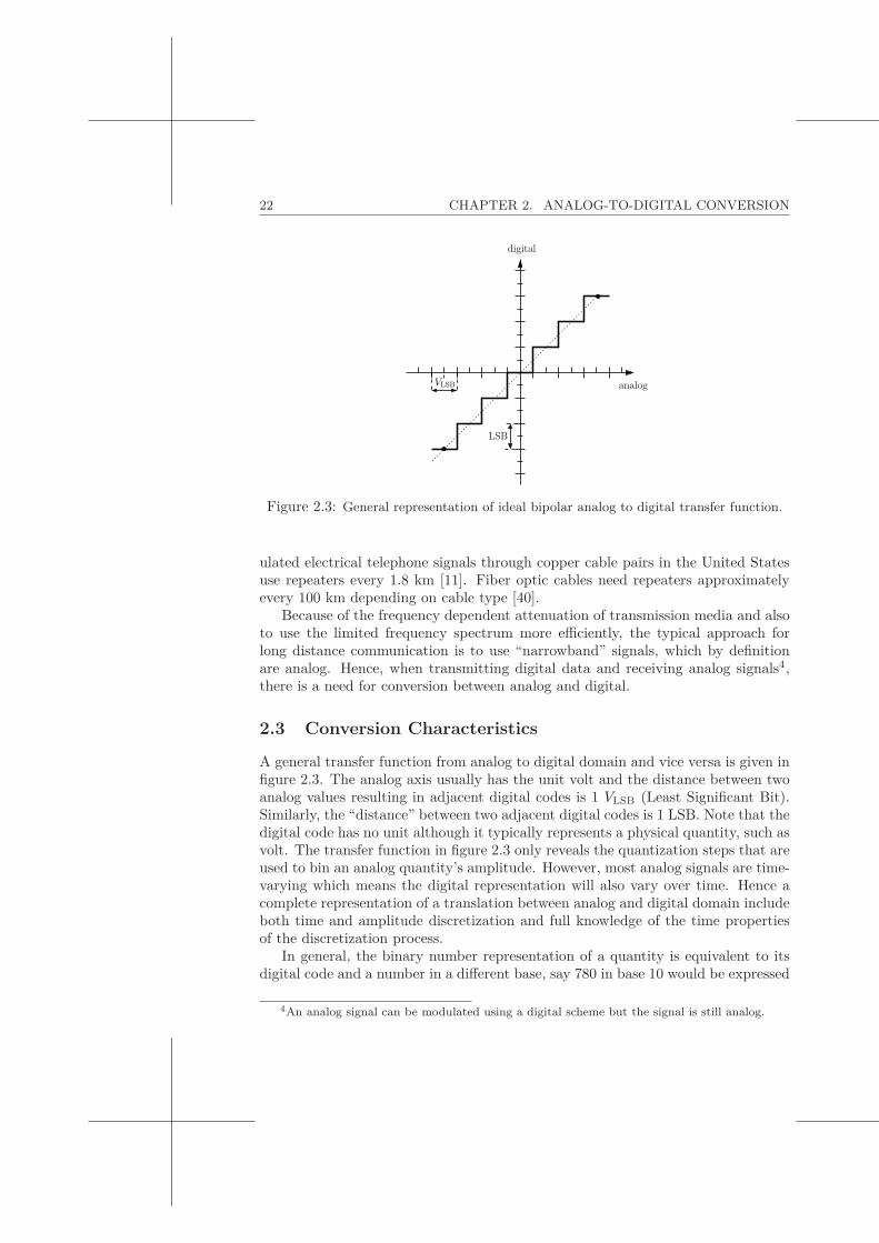
2.3 Conversion Characteristics
A general transfer function from analog to digital domain and vice versa is given infigure 2.3. The analog axis usually has the unit volt and the distance between twoanalog values resulting in adjacent digital codes is 1 VLSB (Least Significant Bit).Similarly, the “distance” between two adjacent digital codes is 1 LSB. Note that thedigital code has no unit although it typically represents a physical quantity, such asvolt. The transfer function in figure 2.3 only reveals the quantization steps that areused to bin an analog quantity’s amplitude. However, most analog signals are time-varying which means the digital representation will also vary over time. Hence acomplete representation of a translation between analog and digital domain includeboth time and amplitude discretization and full knowledge of the time propertiesof the discretization process.
In general, the binary number representation of a quantity is equivalent to itsdigital code and a number in a different base, say 780 in base 10 would be expressed
4An analog signal can be modulated using a digital scheme but the signal is still analog.

2.3. CONVERSION CHARACTERISTICS 23
as
78010 = 512 + 256 + 8 + 4 = 1 · 29 + 1 · 28 + 0 · 27 + 0 · 26+
+ 0 · 25 + 0 · 24 + 1 · 23 + 1 · 22 + 0 · 21 + 0 · 20 = 11000011002 (2.2)
However, in electronic converters the common practice is to use a fixed referenceVref as a max scale indicator and express any quantity as a base 2 fraction of thatreference, i.e.
Vanalog = Vref(b12−1 + b22−2 + · · · + bn2−n
)+ q (2.3)
where n is the resolution5 of the quantizer or converter, b1 is the most significantbit (MSB), bn is the least significant bit (LSB), and q ∈ [−VLSB/2, VLSB/2] is thequantization error. Using the notation from eq. (2.3) we also have VLSB = Vref2−n.
There are different systems for signed binary representation such as
• sign magnitude which uses the MSB for denoting sign6. This system has tworepresentations for the number 0 which means that only 2n − 1 numbers arerepresented using n bits.
• 1’s complement in which negative numbers are the complement of all the bitsin the equivalent positive number. This system also has two representationsfor the number 0.
• offset binary which is equivalent to unipolar binary representation except foran offset such that the most negative number instead of the number 0 has thezero code.
• 2’s complement is equivalent to the offset binary where the MSB denotes signin the same way as the sign magnitude system does. This system has themain advantage that addition of both positive and negative numbers is thesame as ordinary addition and no extra conversion hardware is required.
Manufacturing technology is not perfect and always has limitations in terms of geo-metrical accuracy and physical parameters. Hence, the ideal transfer characteristicshown in figure 2.3 does not reflect the transfer characteristic of a real converter.A real converter will have a transfer characteristic that deviates from the ideal one.Mathematically, an ideal converter transfer characteristic is symmetrically locatedaround a straight line (see fig. 2.3 and 2.4) with the form
D = o+ g ·A (2.4)
5Should not be confused with accuracy which is a measure of the maximum conversion error.For example, 12-bit accuracy means the conversion error is less than the full scale value dividedby 212.
60 for positive and 1 for negative.
24 CHAPTER 2. ANALOG-TO-DIGITAL CONVERSION
987654321 analog [VLSB]
11111111101110111100110111101011001110001011110110101011010010011100101000110000
000010001000011001000010100110001110100001001010100101101100011010111001111
00000
digital
10 11 12 13 14 15 16 17 18 19 20 21 22 23 24 25 26 27 28 29 30 31
ideal transfer line
real transfer line
offset
missing codes
L1 L2
L17
L18
L31
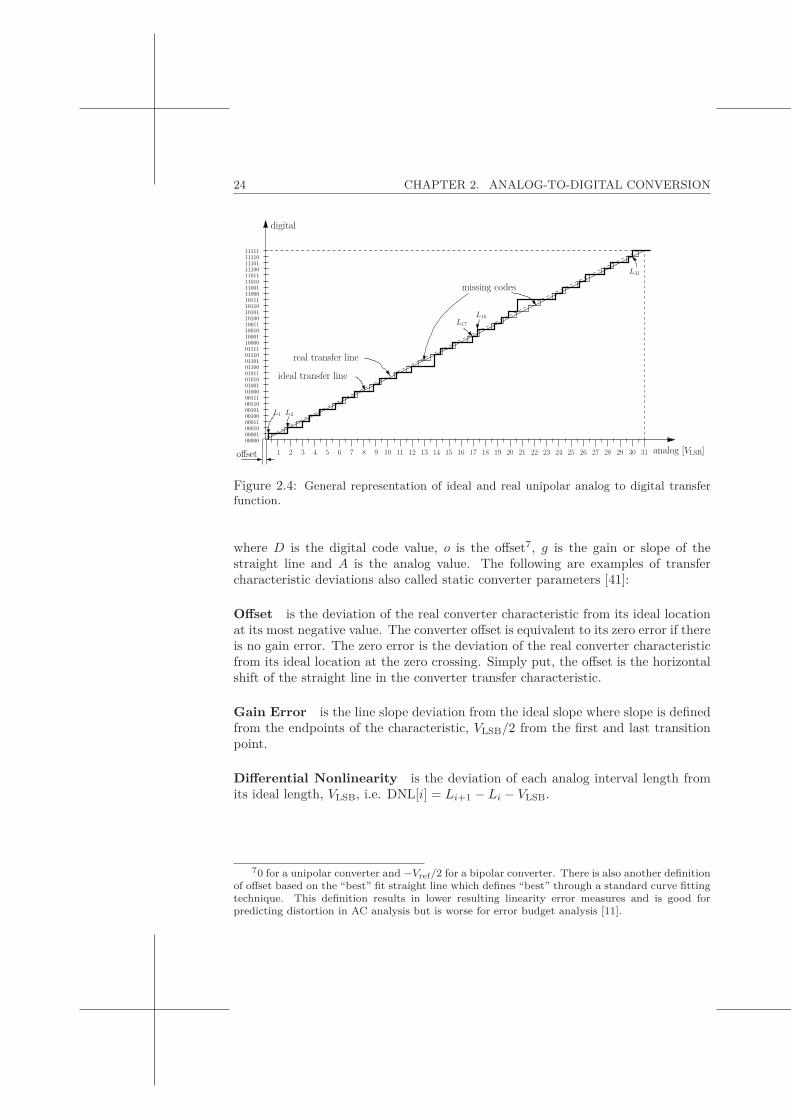
Figure 2.4: General representation of ideal and real unipolar analog to digital transferfunction.
where D is the digital code value, o is the offset7, g is the gain or slope of thestraight line and A is the analog value. The following are examples of transfercharacteristic deviations also called static converter parameters [41]:
Offset is the deviation of the real converter characteristic from its ideal locationat its most negative value. The converter offset is equivalent to its zero error if thereis no gain error. The zero error is the deviation of the real converter characteristicfrom its ideal location at the zero crossing. Simply put, the offset is the horizontalshift of the straight line in the converter transfer characteristic.
Gain Error is the line slope deviation from the ideal slope where slope is definedfrom the endpoints of the characteristic, VLSB/2 from the first and last transitionpoint.
Differential Nonlinearity is the deviation of each analog interval length fromits ideal length, VLSB, i.e. DNL[i] = Li+1 − Li − VLSB.
70 for a unipolar converter and −Vref/2 for a bipolar converter. There is also another definitionof offset based on the “best” fit straight line which defines “best” through a standard curve fittingtechnique. This definition results in lower resulting linearity error measures and is good forpredicting distortion in AC analysis but is worse for error budget analysis [11].
2.3. CONVERSION CHARACTERISTICS 25
Integral Nonlinearity is the cumulative sum of differential nonlinearity, i.e.
INL[i] =i∑
k=1
DNL[k] =i∑
k=1
(Lk+1 − Lk − VLSB
)= Li+1 − L1 − iVLSB (2.5)
Examples of dynamic or frequency domain conversion characteristics are:
Signal-to-Noise Ratio or Dynamic Range (SNR or DR) is the ratio of therms value of the maximum amplitude input signal and the rms value of the outputnoise [42, 43]. Similarly, the signal-to-noise-and-distortion ratio (SNDR8) is definedas the ratio of the rms value of the maximum amplitude input signal and the rmsvalue of the output noise plus distortion.
Spurious-Free Dynamic Range (SFDR) is the ratio of the amplitude of thesignal at the fundamental frequency and the largest spurious signal at the outputof the converter observed over the full Nyquist9 band [44].
Effective Number Of Bits (ENOB) is the representation, in bits, of SNDRgiven in dB and is defined as
ENOB =SNDR − 1.76 dB
6.02 dB/bit (2.6)
The background to this definition is an underlying assumption of quantization errorand signal independence10. By observing the converter characteristic in figs. 2.3and 2.4, it is clear that the quantization error is in the range [−VLSB/2, VLSB/2] fora nonoverloaded converter. Assuming the quantization error has equal probabilityto be anywhere in this range, its mean square value, i.e. power, is
q2RMS =1
VLSB
∫ VLSB/2
−VLSB/2
q2dq =V 2
LSB12
(2.7)
and hence the rms value is qRMS = VLSB/√
12. A full scale sinusoidal input signalhas the rms value Vin,RMS = Vref/(2
√2) = 2nVLSB/(2
√2) according to eq. (2.3)
8Also known as SINAD according to the IEEE 1241 standard [44].9The Nyquist bandwidth corresponding to a signal bandwidth of fB is defined as 2fB and
represents the theoretically lowest sampling frequency needed for being able to reconstruct ananalog signal, having a certain bandwidth, without error after sampling.
10This is obviously not true according to eq. (2.3). However, results using this assumption havebeen verified by experiments to be useful except when the input is constant or changes regularlyby multiples or submultiples of VLSB between samples [20].

26 CHAPTER 2. ANALOG-TO-DIGITAL CONVERSION
and thus the signal-to-quantization-noise ratio (SQNR) is
SQNR = 20 log(Vin,RMSqRMS
)= 20 log
( Vref√
12VLSB · 2√2
)=
= 20 log(
2n
√32
)= 1.76 + 6.02n [dB] (2.8)
The above equation is relating resolution with SQNR and hence ENOB is a measureof how much additional noise, expressed as a reduction in resolution, is in theconverter system.
A common way of comparing different converters’ power efficiency is throughthe measure of quantization energy [24] suggested in a somewhat different forminitially by the analog program committee of the IEEE International Solid-StateCircuits Conference. It takes into account resolution, power dissipation and effectiveresolution bandwidth and is expressed as (cf. Appendix A)
EQ =P
2N (2fB)(2.9)
where P is the power dissipation, N is the high frequency ENOB calculated from theSNDR, and fB is the minimum of the effective resolution bandwidth and Nyquistfrequency.
2.4 Examples of Converters
There are many types of Analog-to-Digital and Digital-to-Analog Converters withdifferences at both architecture and circuit level. This introduction will restrictitself by focusing on Analog-to-Digital Converters. Following is a brief descriptionof ADCs together with some typical characteristics [42].
Integrating Converters operate by counting time. A dual phase integratingconverter (see fig. 2.5) has an operation cycle divided into two phases. The firstphase has a fixed amount of time during which a known capacitor C is chargedby the unknown analog voltage. The second phase consists of a constant slopephase where the accumulated charge is dissipated in a controlled way and thedischarge time is measured. By comparing the discharge and charge-up times,a measure of the unknown voltage can be obtained. Nowadays, multiple phaseintegrating converters are used that operate on the same principles as the dualphase integrating converter. Integrating converters have high accuracy but onlywork for low signal frequencies and are mainly used in measurement applicationssuch as digital voltmeters.

2.4. EXAMPLES OF CONVERTERS 27
fclk
+
−
integrator
comparator
control logic
C
R
timer
digitaloutputreference
analog input
...
Figure 2.5: Block diagram of dual slope integrating Analog-to-Digital Converter.
(b)
s2
s3b1
4C 2C C C
s1s2s3
....
....bnbn−1bn−2
2n−1Csuccessive approximation
register & control logic
b1
b2
Vin
Vref
s1
....
....
......
......
bn
register & control logic
successive approximation
(a)
sample & hold
Vin
comparator
DAC
digitaloutput
s1 s2
C
......
....
Figure 2.6: Block diagram of (a) general SA ADC and (b) unipolar charge-redistributionDAC successive approximation ADC [42].
Successive Approximation Converters are popular converters due to theirreasonably fast11 conversion time and moderate circuit complexity. They operatemuch in the same way as a binary search algorithm by dividing the digital searchspace in two each time a comparison is made with the unknown analog voltage.This way, the desired data can be found in n steps if the digital search space hasa size of 2n. Example architectures of successive approximation (SA) convertersare shown in figure 2.6. The successive approximation converter operates by sam-pling the unknown signal and comparing it with its digital approximation in analog
11Recently reached the MHz range [11]
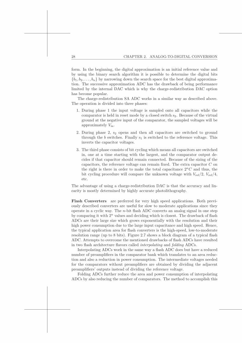
28 CHAPTER 2. ANALOG-TO-DIGITAL CONVERSION
form. In the beginning, the digital approximation is an initial reference value andby using the binary search algorithm it is possible to determine the digital bits{b1, b2, . . . , bn} by narrowing down the search space for the best digital approxima-tion. The successive approximation ADC has the drawback of being performancelimited by the internal DAC which is why the charge-redistribution DAC optionhas become popular.
The charge-redistribution SA ADC works in a similar way as described above.The operation is divided into three phases:
1. During phase 1 the input voltage is sampled onto all capacitors while thecomparator is held in reset mode by a closed switch s2. Because of the virtualground at the negative input of the comparator, the sampled voltages will beapproximately Vin.
2. During phase 2, s2 opens and then all capacitors are switched to groundthrough the b switches. Finally s1 is switched to the reference voltage. Thisinverts the capacitor voltages.
3. The third phase consists of bit cycling which means all capacitors are switchedin, one at a time starting with the largest, and the comparator output de-cides if that capacitor should remain connected. Because of the sizing of thecapacitors, the reference voltage can remain fixed. The extra capacitor C onthe right is there in order to make the total capacitance 2nC and thus, thebit cycling procedure will compare the unknown voltage with Vref/2, Vref/4,etc.
The advantage of using a charge-redistribution DAC is that the accuracy and lin-earity is mostly determined by highly accurate photolithography.
Flash Converters are preferred for very high speed applications. Both previ-ously described converters are useful for slow to moderate applications since theyoperate in a cyclic way. The n-bit flash ADC converts an analog signal in one stepby comparing it with 2n values and deciding which is closest. The drawback of flashADCs are their large size which grows exponentially with the resolution and theirhigh power consumption due to the large input capacitance and high speed. Hence,the typical application area for flash converters is the high-speed, low-to-moderateresolution range (up to 8 bits). Figure 2.7 shows a block diagram of a typical flashADC. Attempts to overcome the mentioned drawbacks of flash ADCs have resultedin two flash architecture flavors called interpolating and folding ADCs.
Interpolating ADCs work in the same way a flash ADC does but have a reducednumber of preamplifiers in the comparator bank which translates to an area reduc-tion and also a reduction in power consumption. The intermediate voltages neededfor the comparators without preamplifiers are obtained by dividing the adjacentpreamplifiers’ outputs instead of dividing the reference voltage.
Folding ADCs further reduce the area and power consumption of interpolatingADCs by also reducing the number of comparators. The method to accomplish this
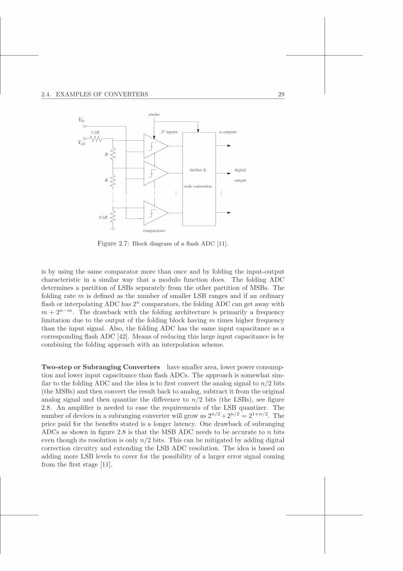
2.4. EXAMPLES OF CONVERTERS 29
strobe
Vref
Vin
output
digital
0.5R
1.5R
R
R
......
..........
n outputs2n inputs
......
......
......
code conversion
latches &
comparators
Figure 2.7: Block diagram of a flash ADC [11].
is by using the same comparator more than once and by folding the input-outputcharacteristic in a similar way that a modulo function does. The folding ADCdetermines a partition of LSBs separately from the other partition of MSBs. Thefolding rate m is defined as the number of smaller LSB ranges and if an ordinaryflash or interpolating ADC has 2n comparators, the folding ADC can get away withm + 2n−m. The drawback with the folding architecture is primarily a frequencylimitation due to the output of the folding block having m times higher frequencythan the input signal. Also, the folding ADC has the same input capacitance as acorresponding flash ADC [42]. Means of reducing this large input capacitance is bycombining the folding approach with an interpolation scheme.
Two-step or Subranging Converters have smaller area, lower power consump-tion and lower input capacitance than flash ADCs. The approach is somewhat sim-ilar to the folding ADC and the idea is to first convert the analog signal to n/2 bits(the MSBs) and then convert the result back to analog, subtract it from the originalanalog signal and then quantize the difference to n/2 bits (the LSBs), see figure2.8. An amplifier is needed to ease the requirements of the LSB quantizer. Thenumber of devices in a subranging converter will grow as 2n/2 +2n/2 = 21+n/2. Theprice paid for the benefits stated is a longer latency. One drawback of subrangingADCs as shown in figure 2.8 is that the MSB ADC needs to be accurate to n bitseven though its resolution is only n/2 bits. This can be mitigated by adding digitalcorrection circuitry and extending the LSB ADC resolution. The idea is based onadding more LSB levels to cover for the possibility of a larger error signal comingfrom the first stage [11].
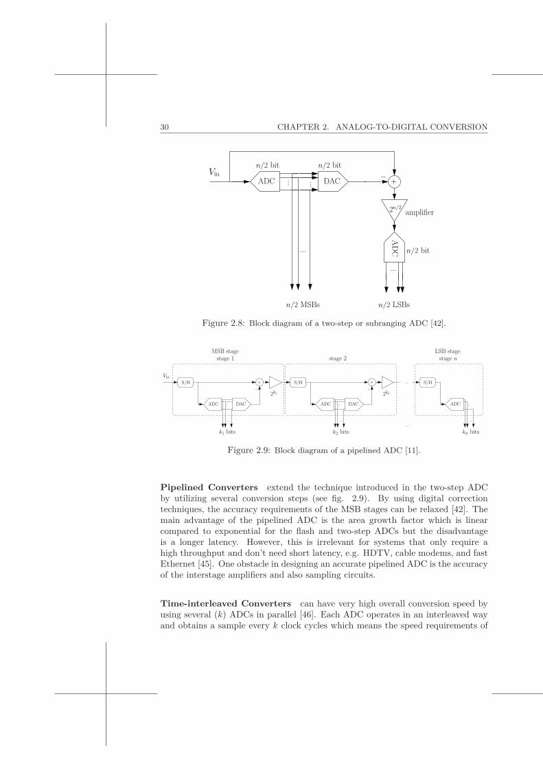
30 CHAPTER 2. ANALOG-TO-DIGITAL CONVERSION
...
AD
C
DAC...ADC ......
n/2 bit
n/2 MSBs
+−
n/2 LSBs
n/2 bit
n/2 bit
Vin
amplifier2n/2
Figure 2.8: Block diagram of a two-step or subranging ADC [42].
LSB stageMSB stagestage 1
VinS/H
...ADC DAC
+
−
...
stage 2
... S/H
...
stage n
ADC ...
......
−+
DACADC ...
S/H
2k1 2k2
k1 bits k2 bits kn bits
Figure 2.9: Block diagram of a pipelined ADC [11].
Pipelined Converters extend the technique introduced in the two-step ADCby utilizing several conversion steps (see fig. 2.9). By using digital correctiontechniques, the accuracy requirements of the MSB stages can be relaxed [42]. Themain advantage of the pipelined ADC is the area growth factor which is linearcompared to exponential for the flash and two-step ADCs but the disadvantageis a longer latency. However, this is irrelevant for systems that only require ahigh throughput and don’t need short latency, e.g. HDTV, cable modems, and fastEthernet [45]. One obstacle in designing an accurate pipelined ADC is the accuracyof the interstage amplifiers and also sampling circuits.
Time-interleaved Converters can have very high overall conversion speed byusing several (k) ADCs in parallel [46]. Each ADC operates in an interleaved wayand obtains a sample every k clock cycles which means the speed requirements of
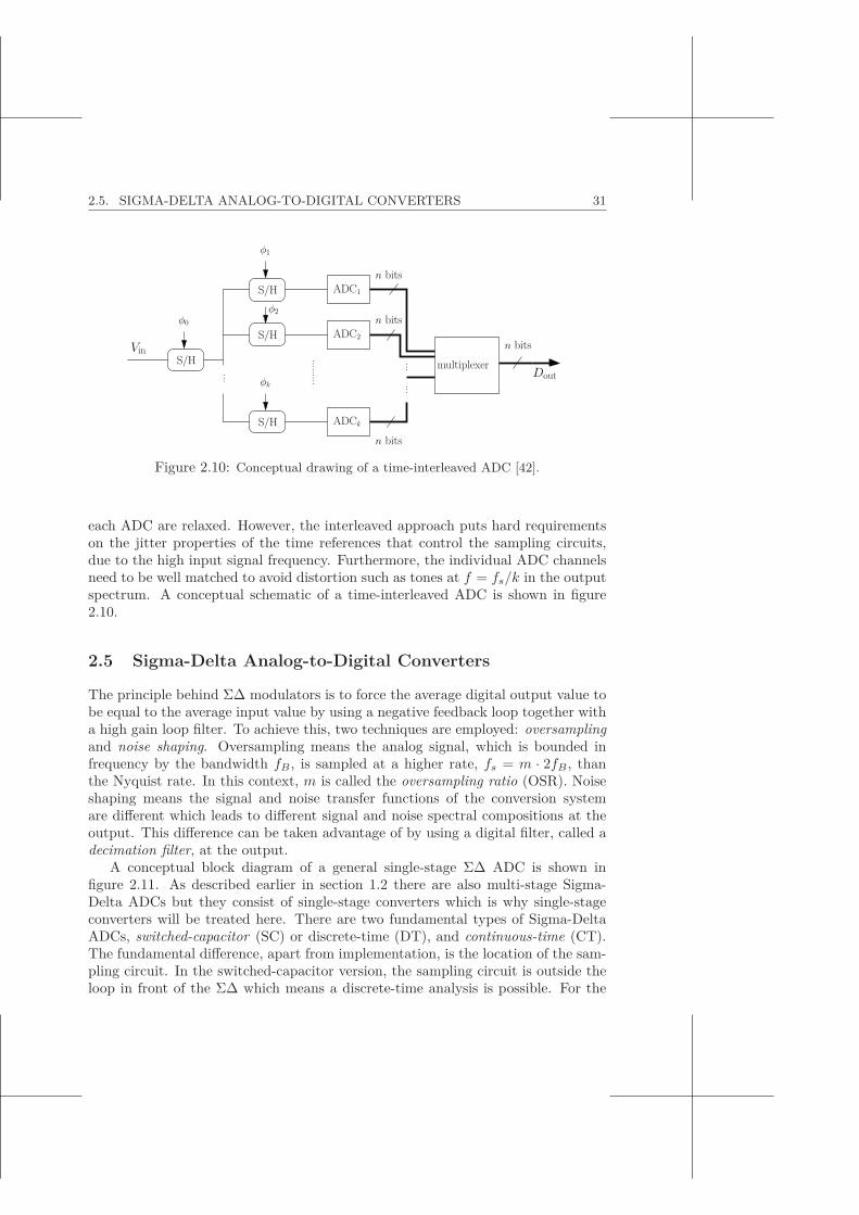
2.5. SIGMA-DELTA ANALOG-TO-DIGITAL CONVERTERS 31
Dout
Vin
ADCk
n bits
n bits
n bits
n bits
φk
φ2
φ1
φ0
multiplexer......
ADC2
ADC1
... ......
...
S/H
S/H
S/H
S/H
Figure 2.10: Conceptual drawing of a time-interleaved ADC [42].
each ADC are relaxed. However, the interleaved approach puts hard requirementson the jitter properties of the time references that control the sampling circuits,due to the high input signal frequency. Furthermore, the individual ADC channelsneed to be well matched to avoid distortion such as tones at f = fs/k in the outputspectrum. A conceptual schematic of a time-interleaved ADC is shown in figure2.10.
2.5 Sigma-Delta Analog-to-Digital Converters
The principle behind ΣΔ modulators is to force the average digital output value tobe equal to the average input value by using a negative feedback loop together witha high gain loop filter. To achieve this, two techniques are employed: oversamplingand noise shaping. Oversampling means the analog signal, which is bounded infrequency by the bandwidth fB , is sampled at a higher rate, fs = m · 2fB , thanthe Nyquist rate. In this context, m is called the oversampling ratio (OSR). Noiseshaping means the signal and noise transfer functions of the conversion systemare different which leads to different signal and noise spectral compositions at theoutput. This difference can be taken advantage of by using a digital filter, called adecimation filter, at the output.
A conceptual block diagram of a general single-stage ΣΔ ADC is shown infigure 2.11. As described earlier in section 1.2 there are also multi-stage Sigma-Delta ADCs but they consist of single-stage converters which is why single-stageconverters will be treated here. There are two fundamental types of Sigma-DeltaADCs, switched-capacitor (SC) or discrete-time (DT), and continuous-time (CT).The fundamental difference, apart from implementation, is the location of the sam-pling circuit. In the switched-capacitor version, the sampling circuit is outside theloop in front of the ΣΔ which means a discrete-time analysis is possible. For the
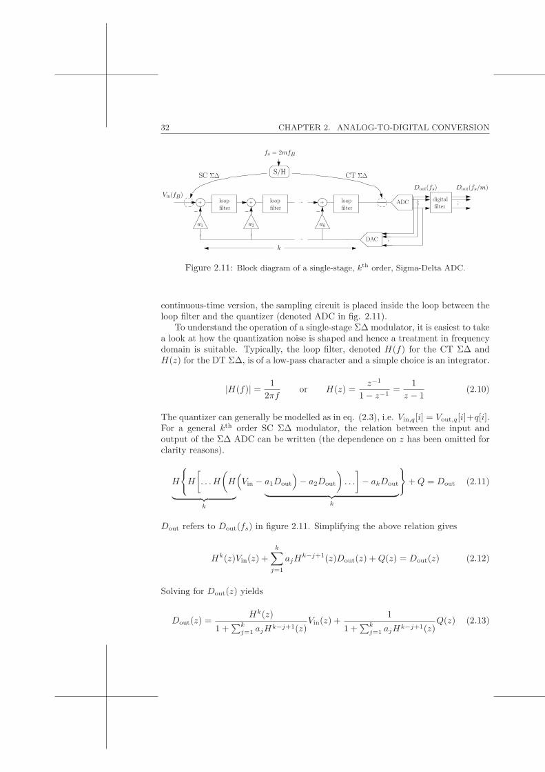
32 CHAPTER 2. ANALOG-TO-DIGITAL CONVERSION
fs = 2mfB
+
−loopfilter
+ loopfilter−
...
...
− filterloop ...ADC
...DAC
+
SC ΣΔ CT ΣΔ
k
Vin(fB)Dout(fs/m)
...
filterdigital
Dout(fs)
S/H
a1 a2 ak
Figure 2.11: Block diagram of a single-stage, kth order, Sigma-Delta ADC.
continuous-time version, the sampling circuit is placed inside the loop between theloop filter and the quantizer (denoted ADC in fig. 2.11).
To understand the operation of a single-stage ΣΔ modulator, it is easiest to takea look at how the quantization noise is shaped and hence a treatment in frequencydomain is suitable. Typically, the loop filter, denoted H(f) for the CT ΣΔ andH(z) for the DT ΣΔ, is of a low-pass character and a simple choice is an integrator.
|H(f)| =1
2πfor H(z) =
z−1
1 − z−1=
1z − 1
(2.10)
The quantizer can generally be modelled as in eq. (2.3), i.e. Vin,q[i] = Vout,q[i]+q[i].For a general kth order SC ΣΔ modulator, the relation between the input andoutput of the ΣΔ ADC can be written (the dependence on z has been omitted forclarity reasons).
H
{H
[. . . H
(H
︸ ︷︷ ︸k
(Vin − a1Dout
)− a2Dout
). . .
]− akDout︸ ︷︷ ︸
k
}+Q = Dout (2.11)
Dout refers to Dout(fs) in figure 2.11. Simplifying the above relation gives
Hk(z)Vin(z) +k∑
j=1
ajHk−j+1(z)Dout(z) +Q(z) = Dout(z) (2.12)
Solving for Dout(z) yields
Dout(z) =Hk(z)
1 +∑k
j=1 ajHk−j+1(z)Vin(z) +
1
1 +∑k
j=1 ajHk−j+1(z)Q(z) (2.13)
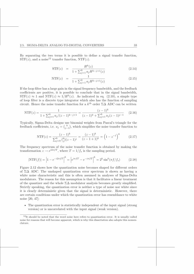
2.5. SIGMA-DELTA ANALOG-TO-DIGITAL CONVERTERS 33
By separating the two terms it is possible to define a signal transfer function,STF(z), and a noise12 transfer function, NTF(z).
STF(z) =Hk(z)
1 +∑k
j=1 ajHk−j+1(z)(2.14)
NTF(z) =1
1 +∑k
j=1 ajHk−j+1(z)(2.15)
If the loop filter has a large gain in the signal frequency bandwidth, and the feedbackcoefficients are positive, it is possible to conclude that in the signal bandwidth,STF(z) ≈ 1 and NTF(z) ≈ 1/Hk(z). As indicated in eq. (2.10), a simple typeof loop filter is a discrete type integrator which also has the function of samplingcircuit. Hence the noise transfer function for a kth order ΣΔ ADC can be written
NTF(z) =1
1 +∑k
j=1 aj/(z − 1)k−j+1=
(z − 1)k
(z − 1)k +∑k
j=1 aj(z − 1)j−1(2.16)
Typically, Sigma-Delta designs use binomial weights from Pascal’s triangle for thefeedback coefficients, i.e. aj =
(k
j−1
), which simplifies the noise transfer function to
NTF(z) =(z − 1)k∑k
j=0
(kj
)(z − 1)j
=(z − 1)k
(z − 1 + 1)k=
(1 − z−1
)k
(2.17)
The frequency spectrum of the noise transfer function is obtained by making thetransformation z → ei2πfT , where T = 1/fs is the sampling period.
|NTF(f)| =∣∣∣1 − e−i2πfT
∣∣∣k =∣∣∣eiπfT − e−iπfT
∣∣∣k = 2k sink(πf/fs) (2.18)
Figure 2.12 shows how the quantization noise becomes shaped for different ordersof ΣΔ ADC. The unshaped quantization error spectrum is shown as having awhite noise characteristic and this is often assumed in analyses of Sigma-Deltamodulators. The reason for this assumption is that it facilitates a linear treatmentof the quantizer and the whole ΣΔ modulator analysis becomes greatly simplified.Strictly speaking, the quantization error is neither a type of noise nor white sinceit is clearly deterministic given that the signal is deterministic. However, thereare certain conditions under which the quantization error has resemblance to whitenoise [20, 47]:
• The quantization error is statistically independent of the input signal (strongversion) or is uncorrelated with the input signal (weak version).
12It should be noted that the word noise here refers to quantization error. It is usually callednoise for reasons that will become apparent, which is why this dissertation also adopts this nomen-clature.
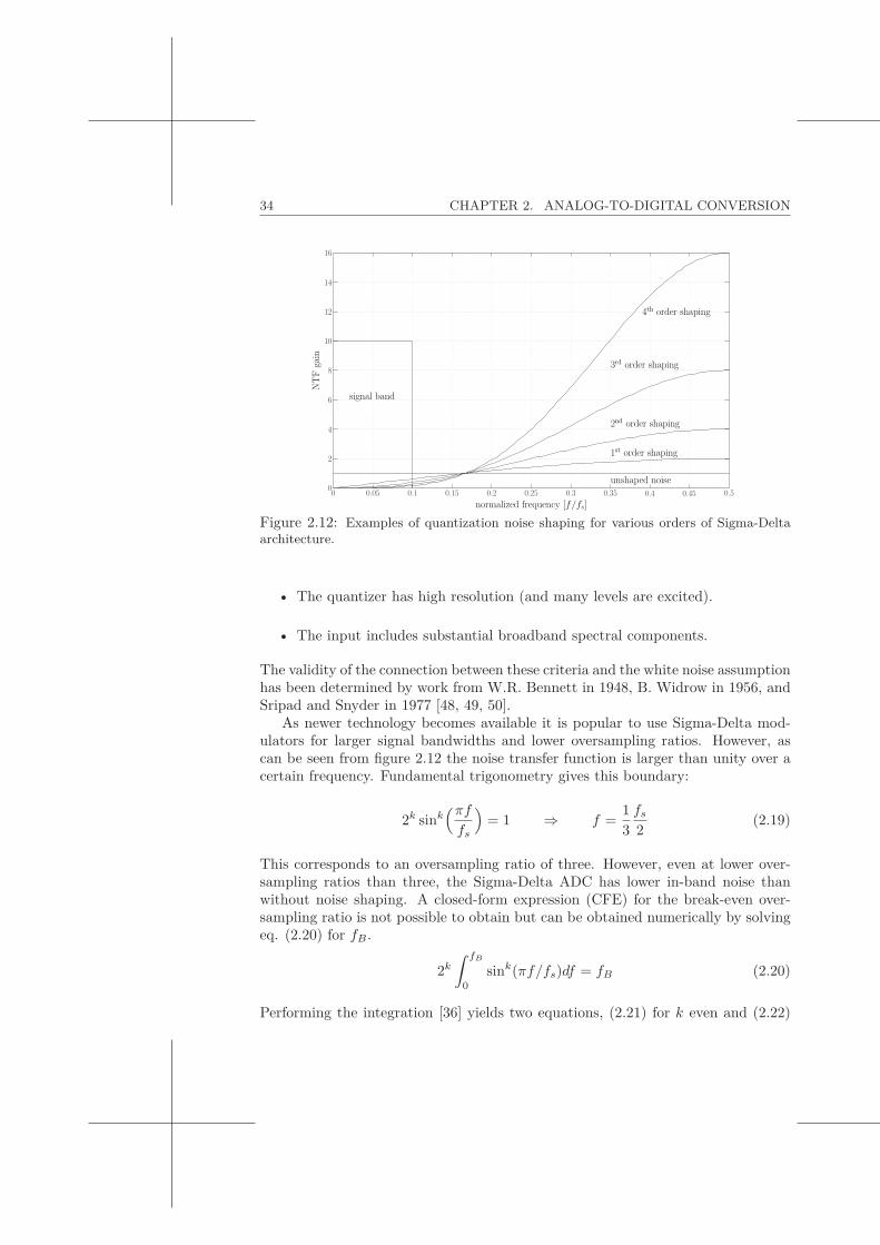
34 CHAPTER 2. ANALOG-TO-DIGITAL CONVERSION
normalized frequency [f/fs]
NTF
gain
unshaped noise
1st order shaping
2nd order shaping
3rd order shaping
signal band
4th order shaping
0 0.05 0.1 0.15 0.2 0.25 0.3 0.35 0.4 0.45 0.50
2
4
6
8
10
12
14
16
Figure 2.12: Examples of quantization noise shaping for various orders of Sigma-Deltaarchitecture.
• The quantizer has high resolution (and many levels are excited).
• The input includes substantial broadband spectral components.
The validity of the connection between these criteria and the white noise assumptionhas been determined by work from W.R. Bennett in 1948, B. Widrow in 1956, andSripad and Snyder in 1977 [48, 49, 50].
As newer technology becomes available it is popular to use Sigma-Delta mod-ulators for larger signal bandwidths and lower oversampling ratios. However, ascan be seen from figure 2.12 the noise transfer function is larger than unity over acertain frequency. Fundamental trigonometry gives this boundary:
2k sink(πffs
)= 1 ⇒ f =
13fs
2(2.19)
This corresponds to an oversampling ratio of three. However, even at lower over-sampling ratios than three, the Sigma-Delta ADC has lower in-band noise thanwithout noise shaping. A closed-form expression (CFE) for the break-even over-sampling ratio is not possible to obtain but can be obtained numerically by solvingeq. (2.20) for fB .
2k
∫ fB
0
sink(πf/fs)df = fB (2.20)
Performing the integration [36] yields two equations, (2.21) for k even and (2.22)
2.5. SIGMA-DELTA ANALOG-TO-DIGITAL CONVERTERS 35
Table 2.1: Break Even OSR and signal bandwidth
order k OSR bandwidth [fs]k = 1 m ≈ 1.41 fB ≈ 0.36k = 2 m ≈ 1.66 fB ≈ 0.3k = 3 m ≈ 1.82 fB ≈ 0.275k = 4 m ≈ 1.95 fB ≈ 0.257k = 5 m ≈ 2.04 fB ≈ 0.245
for k odd:
(k
k/2
)fB + 2(−1)k/2
( k2−1∑j=0
(−1)j
(k
j
)sin
((k − 2j)πfB/fs
)(k − 2j)π/fs
)= fB (2.21)
2(−1)(k−1)/2
((k−1)/2∑
j=0
(−1)j
(k
j
)1 − cos
((k − 2j)πfB/fs
)(k − 2j)π/fs
)= fB (2.22)
The solutions to these equations for the first five noise shaping orders are given intable 2.1. Obviously, for higher noise shaping orders, the tolerance for wide signalbandwidth goes down. However, typical oversampling ratios are larger than eightwhich means there are apparent benefits of noise shaping order increase.
To calculate the inband SQNR for a Sigma-Delta modulator of arbitrary order,it is assumed that the quantization noise has white noise properties. Hence, itssingle sided spectral density can be obtained from eq. (2.7).
Q(f) =qRMS√fs/2
=VLSB√
6fs
(2.23)
The total inband quantization noise power is given by
Pq,inband =∫ fB
0
Q2(f)NTF2(f)df
=∫ fB
0
V 2LSB6fs
22k sin2k(πf/fs)df (2.24)
For a general expression, the approach from eqs. (2.21) and (2.22) can be used.However, to simplify matters it is assumed that the oversampling ratio m ≥ 8. Atthis OSR, the approximation sin(πf/fs) ≈ πf/fs is fairly accurate for f ∈ [0, fB ]

36 CHAPTER 2. ANALOG-TO-DIGITAL CONVERSION
OSR morder k
SQN
R[d
B]
quantizer resolution n = 1
5 10 15 20 25 30 35 40 45 50
11.522.533.544.5520
40
60
80
100
120
140
160
Figure 2.13: Inband SQNR dependence on noise shaping order, k, and oversamplingratio, m for a single stage Sigma-Delta modulator with a 1 bit quantizer.
and the result becomes
Pq,inband ≈∫ fB
0
V 2LSB6fs
22k(πf/fs)2kdf
≈ π2k V 2LSB
12(2k + 1)
(2fB
fs
)2k+1
≈ π2k
m2k+1
V 2LSB
12(2k + 1)(2.25)
Assuming, without loss of generality, that the Sigma-Delta modulator has an nbit quantizer, then VLSB = Vref/2n. Furthermore, a full scale sinusoid has anamplitude of Vref/2 with the power Psignal = V 2
ref/8 which means the inband signal-to-quantization noise ratio becomes
SQNRinband ≈ 32
2n(2k + 1)π2k
m2k+1 (2.26)
N.B. this relation is approximately true only for m ≥ 8. Figure 2.13 shows how thesignal-to-quantization noise ratio changes when varying the oversampling ratio andnoise shaping order for a 1 bit quantizer resolution13.
13A different resolution will have exactly the same characteristic shape but with a 6 dB upwardshift for every added resolution bit.
Chapter 3Clock Jitter Effects in Switched-CapacitorSigma-Delta ADCs
3.1 Introduction
As previously mentioned, increasing the clock frequency means an increase in tim-ing uncertainty, if the increased frequency is obtained through an increase in thedivision ratio in a PLL. An uncertainty in the time information of the samplestaken from a time-varying analog waveform is equivalent to an uncertainty of thesame waveform’s amplitude since reconstruction is based on known sampling in-stants. Figure 1.9 shows three examples of signals with phase noise that have beenreconstructed at jitter-free time instants. The result is equivalent to a jitter-freesignal sampled and reconstructed by a time reference having uncertainty in thesampling instants. The analog signal contains time information through the am-plitude value’s relation with previous values. In digital form, this information isretained through the known sampling instants since there is no longer a continuouswaveform that determines the behavior of the signal.
The sources of timing or phase noise include any dynamic nonidealities in the en-vironment surrounding the path between the time reference generator and samplingcircuit. Examples are device noise inherent in transistors and resistive elements, am-bient temperature variations, electromagnetic coupling from nearby circuits and/orexternal sources, and coupling through the supply lines or the silicon substrate[51, 52].
Previously published work describing the effects of clock jitter [20, 53, 54] havetreated the sampling circuit as an ideal switch and not considered a real sampler.This approach has several limitations since circuit effects cannot be accounted for.
This chapter presents an analysis of clock jitter effects in a switched-capacitorSigma-Delta modulator at a granularity level one step finer than previous work.The results are easily extended to any ADC utilizing a similar sampling circuit.The author’s publications describing the results in this chapter are [2] and [6] in
37

38 CHAPTER 3. JITTER EFFECTS IN SC SIGMA-DELTA ADCS
Dout[i]V ′
1[i] V2[i] V ′2[i] Vk[i] V ′
k[i]Vin(t)+
−
V1(t)
SC int +
−SC int SC int...
...
−
...ADC
...DAC
+
k
a1 a2 ak
Figure 3.1: Block diagram of the analysed single-stage, kth order, SC Sigma-Delta ADC.
the list of publications.
3.2 Analysis Framework
3.2.1 Circuit StructuresFor verification purposes, a second order switched-capacitor Sigma-Delta ADC hasbeen the simulation basis of this analysis but the theoretical analysis is for a kth
order, single stage structure (see fig. 3.1). The feedback coefficients have beenchosen according to the binomial weights in Pascal’s triangle, as described in theprevious chapter, which means the simulations have used {a1, a2} = {1, 2}.
The loop filters, which also serve as sampling circuits, are switched-capacitorintegrators as shown in figure 3.2. There are several implementation variations forthe feedback mechanism in a SC integrator but this dissertation assumes to havethe following input at time t, during φ1 clock cycle i:
V1(t) = Vin(t) − a1Vfb[i] , j = 1 (3.1)Vj [i] = V ′
j−1[i] − ajVfb[i] , j = 2, 3, . . . , k (3.2)
A circuit level implementation of this functionality is shown e.g. in [55] (fig. 9) or[56] (fig. 4). The location of the integrator, within the ΣΔ modulator, is denotedby j, where j = 1 denotes up-front and j = k denotes in front of the quantizer.It is assumed here and throughout this dissertation, if not otherwise stated, thatthe amplifier is ideal with Zin = ∞ Ω and infinite amplification. The integra-tor operates together with a nonoverlapping clock system consisting of two clocksignals1 {φ1, φ2}. The operation of the integrator is thus divided into two phases:sampling phase and accumulation phase. The switches are modelled as NMOS tran-sistor switches. Hence, the sampling phase is defined as the time intervals duringwhich the φ1 time reference signal is high and the accumulation phase is definedequivalently for the clock signal φ2.
1A thorough analysis of the circuit structure creating two nonoverlapping clock signals froma single clock is described in chapter 6.
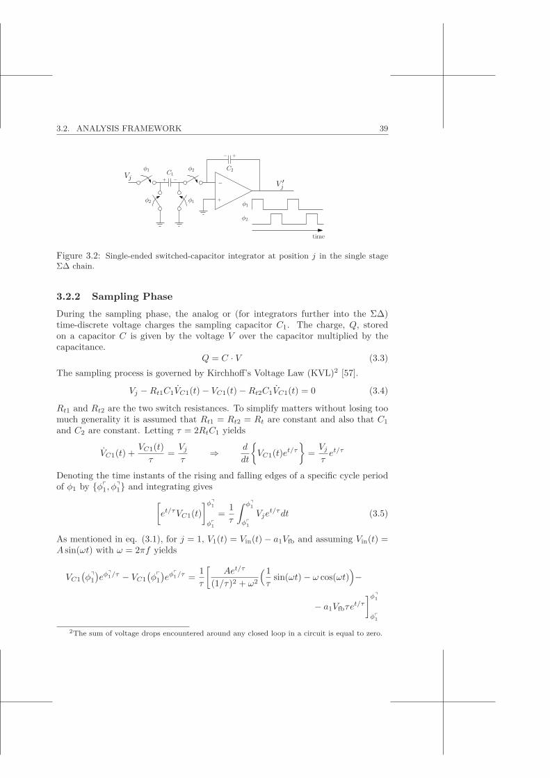
3.2. ANALYSIS FRAMEWORK 39
−
+
+ −
+−
V ′j
VjC1
C2φ1
φ1φ2
φ2
time
φ1
φ2
Figure 3.2: Single-ended switched-capacitor integrator at position j in the single stageΣΔ chain.
3.2.2 Sampling PhaseDuring the sampling phase, the analog or (for integrators further into the ΣΔ)time-discrete voltage charges the sampling capacitor C1. The charge, Q, storedon a capacitor C is given by the voltage V over the capacitor multiplied by thecapacitance.
Q = C · V (3.3)The sampling process is governed by Kirchhoff’s Voltage Law (KVL)2 [57].
Vj −Rt1C1VC1(t) − VC1(t) −Rt2C1VC1(t) = 0 (3.4)
Rt1 and Rt2 are the two switch resistances. To simplify matters without losing toomuch generality it is assumed that Rt1 = Rt2 = Rt are constant and also that C1
and C2 are constant. Letting τ = 2RtC1 yields
VC1(t) +VC1(t)τ
=Vj
τ⇒ d
dt
{VC1(t)et/τ
}=Vj
τet/τ
Denoting the time instants of the rising and falling edges of a specific cycle periodof φ1 by {φ�
1, φ�1} and integrating gives[
et/τVC1(t)]φ�
1
φ�1
=1τ
∫ φ�1
φ�1
Vjet/τdt (3.5)
As mentioned in eq. (3.1), for j = 1, V1(t) = Vin(t) − a1Vfb and assuming Vin(t) =A sin(ωt) with ω = 2πf yields
VC1
(φ�
1
)eφ�
1/τ − VC1
(φ�
1
)eφ�
1/τ =1τ
[Aet/τ
(1/τ)2 + ω2
(1τ
sin(ωt) − ω cos(ωt))−
− a1Vfbτet/τ
]φ�1
φ�1
2The sum of voltage drops encountered around any closed loop in a circuit is equal to zero.
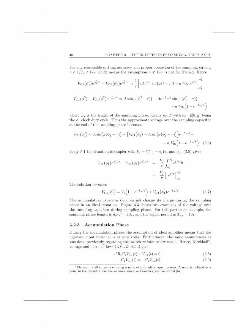
40 CHAPTER 3. JITTER EFFECTS IN SC SIGMA-DELTA ADCS
For any reasonable settling accuracy and proper operation of the sampling circuit,τ < 1/fs < 1/ω which means the assumption τ 1/ω is not far fetched. Hence
VC1
(φ�
1
)eφ�
1/τ − VC1
(φ�
1
)eφ�
1/τ ≈ 1τ
[τAet/τ sin
(ω(t− τ)
)− a1Vfbτet/τ
]φ�1
φ�1
VC1
(φ�
1
)− VC1
(φ�
1
)e−Ls/τ ≈ A sin
(ω(φ�
1 − τ))−Ae−Ls/τ sin
(ω(φ�
1 − τ))−
− a1Vfb
(1 − e−Ls/τ
)where Ls is the length of the sampling phase, ideally dφ1T with dφ1 ∈]0, 1
2 [ beingthe φ1 clock duty cycle. Thus the approximate voltage over the sampling capacitorat the end of the sampling phase becomes
VC1
(φ�
1
) ≈ A sin(ω(φ�
1 − τ))
+(VC1
(φ�
1
)−A sin(ω(φ�
1 − τ)))e−Ls/τ−
− a1Vfb
(1 − e−Ls/τ
)(3.6)
For j �= 1 the situation is simpler with Vj = V ′j−1 − ajVfb and eq. (3.5) gives
VC1
(φ�
1
)eφ�
1/τ − VC1
(φ�
1
)eφ�
1/τ =Vj
τ
∫ φ�1
φ�1
et/τdt
=Vj
τ
[τet/τ
]φ�1
φ�1
The solution becomes
VC1
(φ�
1
)= Vj
(1 − e−Ls/τ
)+ VC1
(φ�
1
)e−Ls/τ (3.7)
The accumulation capacitor C2 does not change its charge during the samplingphase in an ideal situation. Figure 3.3 shows two examples of the voltage overthe sampling capacitor during sampling phase. For this particular example, thesampling phase length is dφ1T = 10τ , and the signal period is Tsig = 10T .
3.2.3 Accumulation PhaseDuring the accumulation phase, the assumption of ideal amplifier means that thenegative input terminal is at zero volts. Furthermore, the same assumptions aswas done previously regarding the switch resistance are made. Hence, Kirchhoff’svoltage and current3 laws (KVL & KCL) give
−2RtC1VC1(t) − VC1(t) = 0 (3.8)C1VC1(t) = −C2VC2(t) (3.9)
3The sum of all currents entering a node of a circuit is equal to zero. A node is defined as apoint in the circuit where two or more wires, or branches, are connected [57].
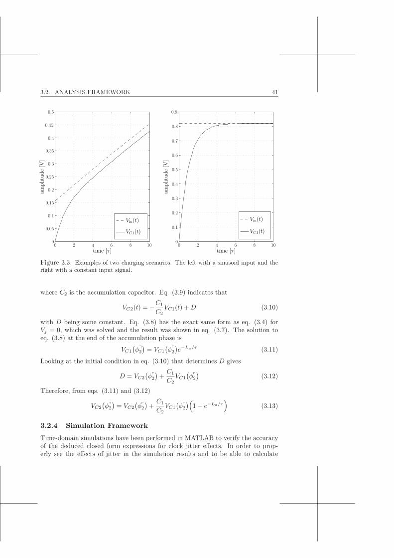
3.2. ANALYSIS FRAMEWORK 41
time [τ ]
ampl
itude
[V]
time [τ ]
ampl
itude
[V]
Vin(t)
VC1(t)
Vin(t)
VC1(t)
0 2 4 6 8 100 2 4 6 8 100
0.1
0.2
0.3
0.4
0.5
0.6
0.7
0.8
0.9
0
0.05
0.1
0.15
0.2
0.25
0.3
0.35
0.4
0.45
0.5
Figure 3.3: Examples of two charging scenarios. The left with a sinusoid input and theright with a constant input signal.
where C2 is the accumulation capacitor. Eq. (3.9) indicates that
VC2(t) = −C1
C2VC1(t) +D (3.10)
with D being some constant. Eq. (3.8) has the exact same form as eq. (3.4) forVj = 0, which was solved and the result was shown in eq. (3.7). The solution toeq. (3.8) at the end of the accumulation phase is
VC1
(φ�
2
)= VC1
(φ�
2
)e−La/τ (3.11)
Looking at the initial condition in eq. (3.10) that determines D gives
D = VC2
(φ�
2
)+C1
C2VC1
(φ�
2
)(3.12)
Therefore, from eqs. (3.11) and (3.12)
VC2
(φ�
2
)= VC2
(φ�
2
)+C1
C2VC1
(φ�
2
)(1 − e−La/τ
)(3.13)
3.2.4 Simulation FrameworkTime-domain simulations have been performed in MATLAB to verify the accuracyof the deduced closed form expressions for clock jitter effects. In order to prop-erly see the effects of jitter in the simulation results and to be able to calculate
42 CHAPTER 3. JITTER EFFECTS IN SC SIGMA-DELTA ADCS
reliable SJNR, the quantization noise has been removed by removing its source,the quantizer. All SJNR calculations have been made using a signal bandwidth offB = fs/2, to maintain generality. However, this means that given white Gaussiannoise (WGN) jitter, the inband SJNR is a factor m higher.
As in the theoretical deductions, it was assumed in the simulations that theintegration amplifiers are ideal. Furthermore, the capacitors in the integrators werescaled such that C1 = C2 = C and the switches were modelled as resistors, havingconstant on-resistance. The sampling frequency was chosen as fs = 96 MHz, theoversampling ratio m = 16, and the clock duty cycle dφ1 = dφ2 = 25%. The analoginput signal was a sinusoid with frequency f = 1.125 MHz and amplitude A = 0.1V, which was 10% of the reference voltage Vref.
The timing jitter has been modelled as WGN with zero mean and constantvariance σ2
j , which modulates the timing instant of each clock edge. Equations (3.6),(3.7), (3.11), and (3.13) were used for modelling the switched-capacitor transferfunction in MATLAB. This allows for a realistic, continuous-time treatment of thetiming uncertainty while the ΣΔ modulator operation, on a macro scale, is modelledin a typical time-discrete way.
3.3 Clock Jitter Definitions
As mentioned in section 1.4, timing jitter is defined as a random fluctuation inthe time instant of an event. Consequently, clock jitter consists of the randomfluctuations of a clock signal’s rise and fall time instants. These instants are relevantsince they control the operation of the switches in a sampling circuit. Figure 3.4shows the two nonoverlapping clock signals {φ1, φ2} together with nomenclature oftiming errors. The transition instants are defined as
φ�1[i] = iT + γ�
φ1[i] φ�1[i] = (i− dφ1)T + γ�
φ1[i] (3.14)φ�
2[i] = (i+ 1/2)T + γ�φ2[i] φ�
2[i] = (i+ 1/2 − dφ2)T + γ�φ2[i] (3.15)
Furthermore, the length of the phases, in a nonoverlap situation, are given by
Ls[i] = φ�1[i] − φ�
1[i] = dφ1T + γ�φ1[i] − γ�
φ1[i] (3.16)La[i] = φ�
2[i] − φ�2[i] = dφ2T + γ�
φ2[i] − γ�φ2[i] (3.17)
Comparing with figure 3.4 the phase length deviations are defined as
δφ1[i] = γ�φ1[i] − γ�
φ1[i] and δφ2[i] = γ�φ2[i] − γ�
φ2[i] (3.18)
There are three distinct effects that can be attributed to the timing uncertaintiesof the combined nonoverlapping clock system:
1. Non-uniform sampling (NUS) effects account for the fact that the samplinginstants, φ�
1, vary stochastically over time.
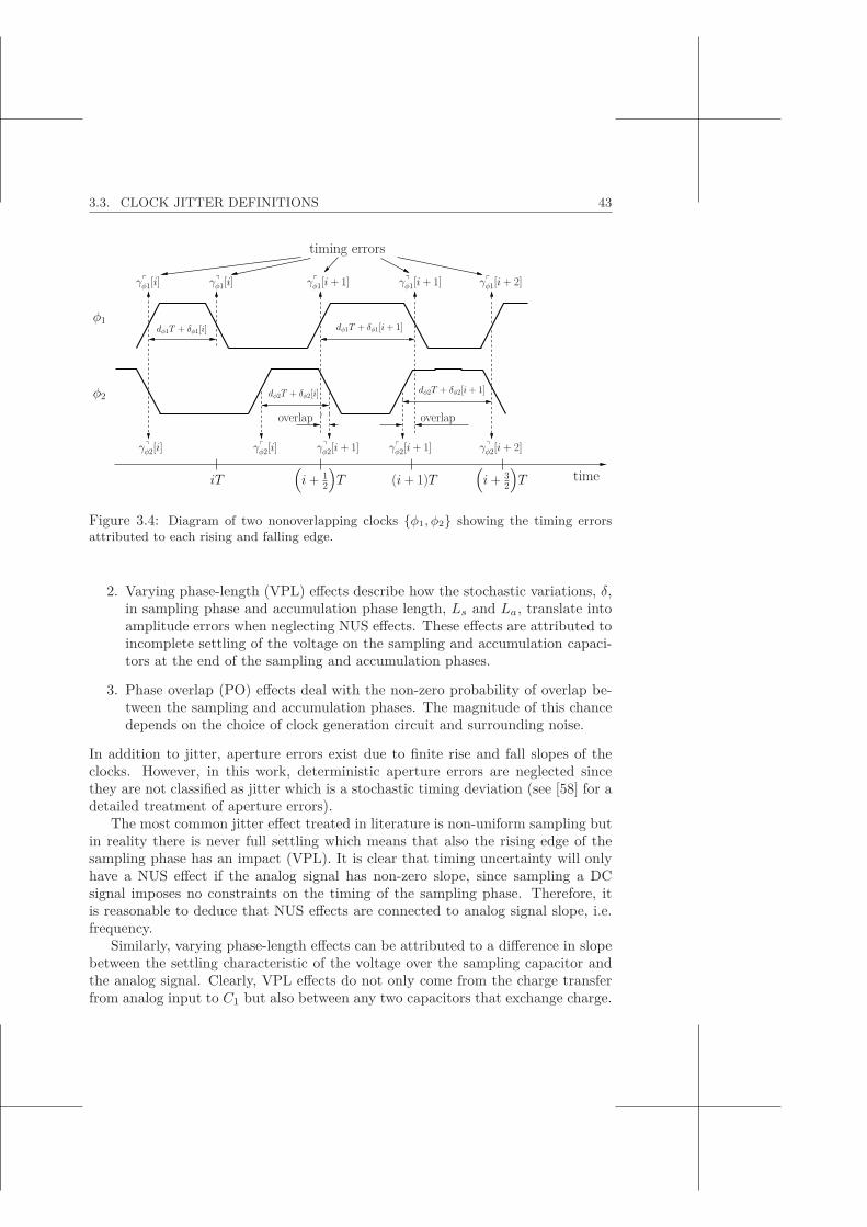
3.3. CLOCK JITTER DEFINITIONS 43
φ2
φ1
(i + 3
2
)T(i + 1)T
(i + 1
2
)TiT
dφ1T + δφ1[i + 1]dφ1T + δφ1[i]
timing errors
dφ2T + δφ2[i + 1]dφ2T + δφ2[i]
overlap overlap
time
γ�φ2[i + 2]γ�
φ2[i + 1]γ�φ2[i + 1]γ�
φ2[i]γ�φ2[i]
γ�φ1[i + 2]γ�
φ1[i + 1]γ�φ1[i] γ�
φ1[i + 1]γ�φ1[i]
Figure 3.4: Diagram of two nonoverlapping clocks {φ1, φ2} showing the timing errorsattributed to each rising and falling edge.
2. Varying phase-length (VPL) effects describe how the stochastic variations, δ,in sampling phase and accumulation phase length, Ls and La, translate intoamplitude errors when neglecting NUS effects. These effects are attributed toincomplete settling of the voltage on the sampling and accumulation capaci-tors at the end of the sampling and accumulation phases.
3. Phase overlap (PO) effects deal with the non-zero probability of overlap be-tween the sampling and accumulation phases. The magnitude of this chancedepends on the choice of clock generation circuit and surrounding noise.
In addition to jitter, aperture errors exist due to finite rise and fall slopes of theclocks. However, in this work, deterministic aperture errors are neglected sincethey are not classified as jitter which is a stochastic timing deviation (see [58] for adetailed treatment of aperture errors).
The most common jitter effect treated in literature is non-uniform sampling butin reality there is never full settling which means that also the rising edge of thesampling phase has an impact (VPL). It is clear that timing uncertainty will onlyhave a NUS effect if the analog signal has non-zero slope, since sampling a DCsignal imposes no constraints on the timing of the sampling phase. Therefore, itis reasonable to deduce that NUS effects are connected to analog signal slope, i.e.frequency.
Similarly, varying phase-length effects can be attributed to a difference in slopebetween the settling characteristic of the voltage over the sampling capacitor andthe analog signal. Clearly, VPL effects do not only come from the charge transferfrom analog input to C1 but also between any two capacitors that exchange charge.

44 CHAPTER 3. JITTER EFFECTS IN SC SIGMA-DELTA ADCS
The settling time constant, τ , determines how accurate the settling is, given a fixedwindow of time for the charge transfer. Of course, a different sampling topologyas the one shown in figure 3.2 might have a different settling characteristic whichmeans that the results presented here might not be applicable in such a case.
Phase overlap is a phenomenon that occurs when the sampling and accumulationphases overlap. How often phase overlap occurs is mainly determined by how severethe timing uncertainty is and the duty cycles of φ1 and φ2. Also, the nonoverlappingclock generation circuit plays a large role in the phase overlap immunity of theclock system. A sufficient combination of negative and positive jitter contributionsin different circuit blocks which process the clocks will give rise to phase overlap.Due to the increasing amount of digital content in deep submicron CMOS, thejitter-inducing power-supply noise and electromagnetic noise levels increase whichleads to higher probability of phase overlap.
From figure 3.4 it is clear that overlap will occur if, considering one clock period,the end of the sampling phase comes later than the beginning of the accumulationphase (case 1) or, vice versa, the end of the accumulation phase comes later thanthe beginning of the sampling phase (case 2). Using the notation from figure 3.4 itis possible to formalize the criterion of phase overlap
φ�1[i] > φ�
2[i] ⇔ γ�φ1[i] − γ�
φ2[i] >(1
2− dφ2
)T (3.19)
φ�2[i] > φ�
1[i+ 1] ⇔ γ�φ2[i] − γ�
φ1[i+ 1] >(1
2− dφ1
)T (3.20)
Defining ε as a measure of the phase overlap magnitude for each period yields
ε1[i] = γ�φ1[i] − γ�
φ2[i] −(1
2− dφ2
)T (3.21)
ε2[i] = γ�φ2[i] − γ�
φ1[i+ 1] −(1
2− dφ1
)T (3.22)
It is assumed, due to the normally small phase overlap probability, that the eventsε1[i] > 0 and ε2[i] > 0 do not occur during the same clock period. Figure 3.5shows the probability density function (PDF) of ε(1,2)[i] with the highlighted areamarking the probability of overlap, i.e. ε(1,2)[i] > 0. The expectation value andvariance of ε(1,2)[i] are trivially obtained from eqs. (3.21) and (3.22).
E{ε(1,2)[i]
}= −
(12− dφ(1,2)
)T V
{ε(1,2)[i]
}= 2σ2
j (3.23)
3.4 Non-Uniform Sampling Effects
Isolating the effects of NUS by neglecting the possibility of phase overlap and as-suming full settling, i.e. no varying phase-length effects, the process of analysingthe non-uniform sampling becomes straightforward. Note that NUS only has animpact in the first integrator since no other sampling circuit operates on an analog

3.4. NON-UNIFORM SAMPLING EFFECTS 45
ε(1,2)[i]
PDF(ε(1,2)[i]
)
−(
12 − dφ(1,2)
)T 0
overlap probability
Figure 3.5: Probability density function of the measure of phase overlap magnitude ε.
signal. Assuming the analog signal is Vin(t) = A sin(ωt), with ω = 2πfsig, whichis sampled at ideal time instants {T, 2T, . . .}, the voltage stored on the samplingcapacitor C1 at the end of sampling phase i is obtained from eq. (3.6) 4
VC1[i] ≈ A sin(ω(iT − τ)
)− a1Vfb[i] (3.24)
During the accumulation phase, this voltage is added onto the existing voltage onthe accumulation capacitor C2. However, for the same reason as why only theup-front integrator matters for NUS effects, the accumulation operation does notintroduce NUS effects. The non-uniform sampling case is similar to eq. (3.24):
VC1[i] ≈ A sin(ω(iT + γ�
φ1[i] − τ))− a1Vfb[i] (3.25)
V is used to denote the nonideal version of V . The difference between eq. (3.25)and eq. (3.24) is the input-referred error signal since this is the input error of anideally clocked SC integrator needed to produce the same output as a non-uniformlysampled SC integrator. Assuming that γ�
φ1[i] is small for all i, an approximation toeq. (3.25) can be made using a first order Taylor expansion around t = iT − τ .
VC1[i] ≈ A sin(ω(iT − τ)
)+Aωγ�
φ1[i] cos(ω(iT − τ)
)− a1Vfb[i] (3.26)
The approximation error of the expansion is bound by
Rmax =A(ωγ�
φ1[i])2
2max
t
{sin(ωt)
}, for t ∈ [
iT − τ, iT − τ + γ�φ1[i]
](3.27)
For jitter magnitudes in the order of 0.1/fs and oversampling ratio m ≥ 8, theapproximation error bound is less than 7.7 · 10−4 · A which is sufficiently accurate
4It should be noted that t[i] and V [i] refer to time t in clock cycle i and voltage value V atthe end of sampling phase i. Similarly, V [i+1/2] refers to voltage value V at end of accumulationphase i.
46 CHAPTER 3. JITTER EFFECTS IN SC SIGMA-DELTA ADCS
for the purposes of this analysis. Therefore, the input-referred error of the integratoris
ΔV1[i] = VC1[i] − VC1[i] ≈ Aωγ�φ1[i] cos
(ω(iT − τ
)+ a1
(Vfb[i] − Vfb[i]
)(3.28)
The second term is a remainder of the memory effects of the ΣΔ modulator and isnot attributed to the injected error at clock cycle i. Thus the jitter-induced errordue to non-uniform sampling becomes
VNUS,in[i] ≈ Aωγ�φ1[i] cos
(ω(iT − τ
)(3.29)
As mentioned before, the following SC integrators in the ΣΔ modulator do not con-tribute to the NUS error power since their input signals are already time-discrete.Therefore, the total input-referred error power is
PNUS,in ≈ (Aω)2V{γ�
φ1[i]}cos2
(ω(iT − τ)
)=
(Aωσj)2
2(3.30)
Thus, the non-uniform error power at the Sigma-Delta modulator output is approx-imately
PNUS,out =PNUS,infs
∫ fs/2
−fs/2
∣∣JTFk(f)∣∣2df = PNUS,in ≈ (Aωσj)2
2(3.31)
where JTFk(f) = 1 is the Jitter Transfer Function from the jitter injection point tothe ΣΔ modulator output. This results in the following approximate SJNR whenassuming full settling and zero probability of phase overlap.
SJNRNUS ≈ 1(ωσj)2
(3.32)
A comparison between eq. (3.32) and simulations performed in MATLAB is shownin figure 3.6. Clearly, the closed-form expression (CFE) accurately predicts theSJNRNUS performance metric.
3.5 Varying Phase-Length Effects
In this section, only VPL effects are considered by neglecting overlap possibilitiesand also NUS effects. When an analog or time-discrete signal is sampled with anideal time reference in a SC integrator of the type shown in figure 3.2, the voltageover the sampling capacitors can be obtained from eqs. (3.6) and (3.7).
VC1[i] ≈ Vin(iT − τ) +(VC1
((i− dφ1)T
)− Vin((i− dφ1)T − τ
))e−dφ1T/τ−
− a1Vfb[i](1 − e−dφ1T/τ
)(3.33)
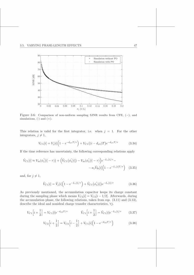
3.5. VARYING PHASE-LENGTH EFFECTS 47
σj [1/fs]
SJN
R[d
B]
Simulation without POSimulation with PO
0 0.02 0.04 0.06 0.08 0.1 0.12 0.14 0.16 0.18 0.220
30
40
50
60
70
80
90
Figure 3.6: Comparison of non-uniform sampling SJNR results from CFE, (−), andsimulations, (·) and (+).
This relation is valid for the first integrator, i.e. when j = 1. For the otherintegrators, j �= 1,
VC1[i] = Vj [i](1 − e−dφ1T/τ
)+ VC1
((i− dφ1)T
)e−dφ1T/τ (3.34)
If the time reference has uncertainty, the following corresponding relations apply
VC1[i] ≈ Vin(φ�1[i] − τ)
)+
(VC1
(φ�
1[i])− Vin(φ�
1[i] − τ))e−Ls[i]/τ−
− a1Vfb[i](1 − e−Ls[i]T/τ
)(3.35)
and, for j �= 1,
VC1[i] = Vj [i](1 − e−Ls[i]/τ
)+ VC1
(φ�
1[i])e−Ls[i]/τ (3.36)
As previously mentioned, the accumulation capacitor keeps its charge constantduring the sampling phase which means VC2[i] = VC2[i− 1/2]. Afterwards, duringthe accumulation phase, the following relations, taken from eqs. (3.11) and (3.13),describe the ideal and nonideal charge transfer characteristics, ∀j.
VC1
[i+
12
]= VC1[i]e−dφ2T/τ VC1
[i+
12
]= VC1[i]e−La[i]/τ (3.37)
VC2
[i+
12
]= VC2
[i− 1
2
]+ VC1[i]
(1 − e−dφ2T/τ
)(3.38)

48 CHAPTER 3. JITTER EFFECTS IN SC SIGMA-DELTA ADCS
VC2
[i+
12
]= VC2
[i− 1
2
]+ VC1[i]
(1 − e−La[i]/τ
)(3.39)
By adopting the notation
Acc1 = e−dφ1T/τ s[i] = e−δφ1[i]/τ (3.40)Acc2 = e−dφ2T/τ a[i] = e−δφ2[i]/τ (3.41)
and noting that VC2[i + 1/2] = VC2[i + 1] = V ′j [i + 1], and using the previous
relations, the ideal and nonideal input-output voltage relations for the first SCintegrator (j = 1) are obtained.
V ′1 [i+ 1] ≈ V ′
1 [i] +[Vin(iT − τ) − Vin
((i− dφ1)T − τ
)Acc1−
− a1Vfb[i](1 −Acc1)](1 −Acc2) (3.42)
V ′1 [i+ 1] ≈ V ′
1 [i] +[Vin(φ�
1[i] − τ) − Vin(φ�
1[i] − τ)Acc1s[i]−
− a1Vfb[i](1 −Acc1s[i]
)](1 −Acc2a[i]) (3.43)
Here, the assumption that VC1[i− 1]Acc2Acc1 is very small has been made. Hence,the injected error in the first SC integrator becomes
Verr,1[i] = ΔV ′1 [i] − ΔV ′
1 [i] =(V ′
1 [i+ 1] − V ′1 [i]
)−
(V ′
1 [i+ 1] − V ′1 [i]
)=
= Vin(φ�1[i] − τ)
(1 −Acc2a[i]
)− Vin(iT − τ)(1 −Acc2)−− Vin(φ�
1[i] − τ)(1 −Acc2a[i]
)Acc1s[i] + Vin
((i− dφ1)T − τ
)Acc1(1 −Acc2)−
− a1Vfb[i](1 −Acc1s[i]
)(1 −Acc2a[i]
)+ a1Vfb[i](1 −Acc1)(1 −Acc2) (3.44)
By neglecting the ΣΔ memory effect terms Vfb[i]− Vfb[i] and non-uniform samplingeffects that are due to input signal slope and also assuming Acc1 ≈ Acc2 = Acc, theinjected error is
Verr,1[i] ≈ Vin(iT − τ)Acc
(1 − a[i]
)+ Vin
((i− dφ1)T − τ
)Acc
(1 − s[i]
)−− a1Vfb[i]Acc
(2 − a[i] − s[i]
)(3.45)
Finally, by recognizing that typically the oversampling ratio is at least 8, the ap-proximation Vin(iT ) ≈ Vin((i− dφ1)T ) is not far fetched. Hence,
Verr,1[i] ≈ Acc
(Vin[i] − a1Vfb[i]
)[2 − a[i] − s[i]
](3.46)
The difficulty in making an accurate estimate of the varying phase-length impactlies in accurately estimating the integrator input signals, e.g. Vin[i] − a1Vfb[i] for
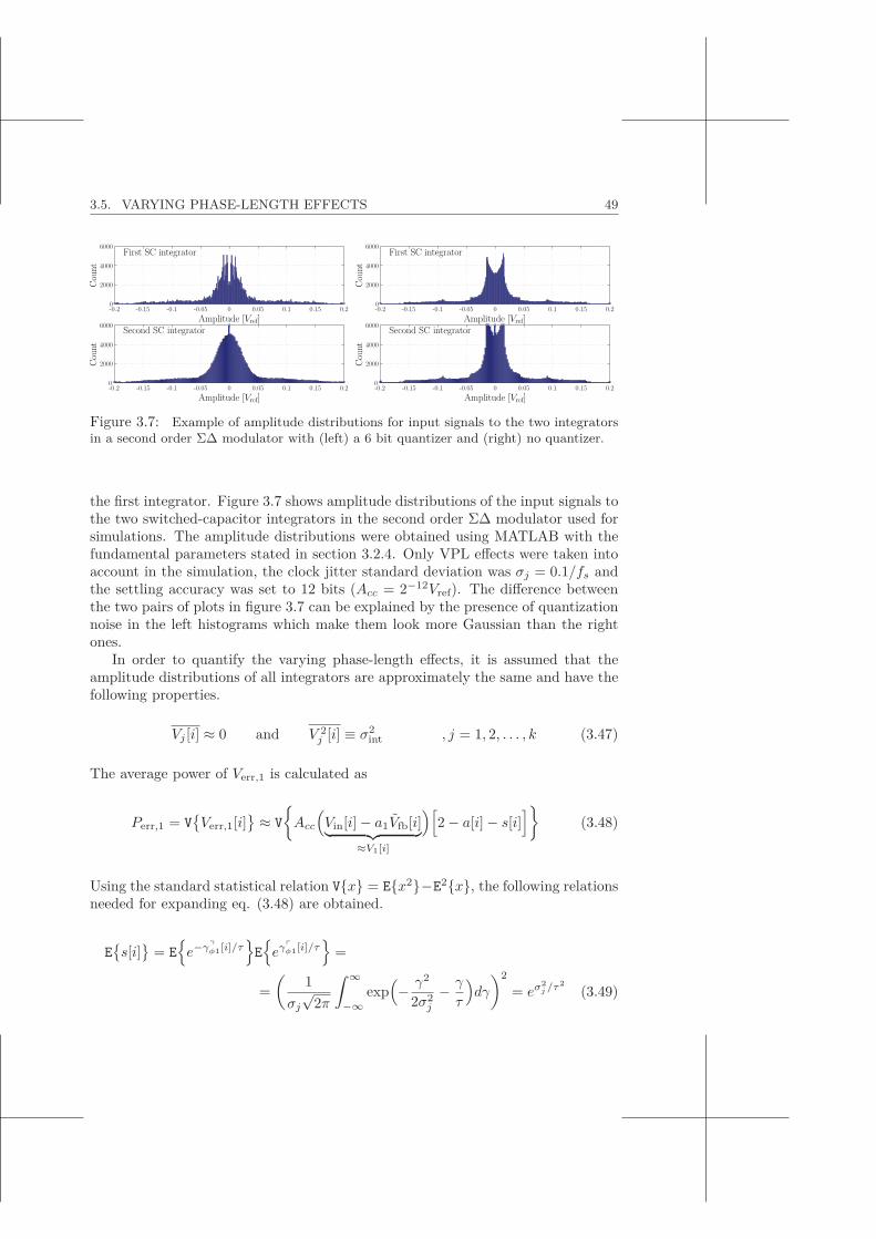
3.5. VARYING PHASE-LENGTH EFFECTS 49
Amplitude [Vref]
Coun
t
Amplitude [Vref]
Coun
t
First SC integrator
Second SC integrator
-0.2 -0.15 -0.1 -0.05 0 0.05 0.1 0.15 0.2
-0.2 -0.15 -0.1 -0.05 0 0.05 0.1 0.15 0.2
0
2000
4000
6000
0
2000
4000
6000
Amplitude [Vref]
Coun
t
Amplitude [Vref]
Coun
t
First SC integrator
Second SC integrator
-0.2 -0.15 -0.1 -0.05 0 0.05 0.1 0.15 0.2
-0.2 -0.15 -0.1 -0.05 0 0.05 0.1 0.15 0.2
0
2000
4000
6000
0
2000
4000
6000
Figure 3.7: Example of amplitude distributions for input signals to the two integratorsin a second order ΣΔ modulator with (left) a 6 bit quantizer and (right) no quantizer.
the first integrator. Figure 3.7 shows amplitude distributions of the input signals tothe two switched-capacitor integrators in the second order ΣΔ modulator used forsimulations. The amplitude distributions were obtained using MATLAB with thefundamental parameters stated in section 3.2.4. Only VPL effects were taken intoaccount in the simulation, the clock jitter standard deviation was σj = 0.1/fs andthe settling accuracy was set to 12 bits (Acc = 2−12Vref). The difference betweenthe two pairs of plots in figure 3.7 can be explained by the presence of quantizationnoise in the left histograms which make them look more Gaussian than the rightones.
In order to quantify the varying phase-length effects, it is assumed that theamplitude distributions of all integrators are approximately the same and have thefollowing properties.
Vj [i] ≈ 0 and V 2j [i] ≡ σ2
int , j = 1, 2, . . . , k (3.47)
The average power of Verr,1 is calculated as
Perr,1 = V{Verr,1[i]
} ≈ V
{Acc
(Vin[i] − a1Vfb[i]︸ ︷︷ ︸
≈V1[i]
)[2 − a[i] − s[i]
]}(3.48)
Using the standard statistical relation V{x} = E{x2}−E2{x}, the following relationsneeded for expanding eq. (3.48) are obtained.
E{s[i]
}= E
{e−γ�
φ1[i]/τ}E{eγ�
φ1[i]/τ}
=
=(
1σj
√2π
∫ ∞
−∞exp
(− γ2
2σ2j
− γ
τ
)dγ
)2
= eσ2j /τ2
(3.49)
50 CHAPTER 3. JITTER EFFECTS IN SC SIGMA-DELTA ADCS
E{s2[i]
}= E
{e−2γ�
φ1[i]/τ}E{e2γ�
φ1[i]/τ}
=
=(
1σj
√2π
∫ ∞
−∞exp
(− γ2
2σ2j
− 2γτ
)dγ
)2
= e4σ2j /τ2
(3.50)
Since the timing uncertainties of both φ1 and φ2 are assumed to have the samestatistical properties, the relations (3.49) and (3.50) also apply to a[i]. Hence
E2{2 − a[i] − s[i]
}= 4
(1 + e2σ2
j /τ2 − 2eσ2j /τ2
)(3.51)
E{(
2 − a[i] − s[i])2
}= 4 − 8eσ2
j /τ2+ 2e2σ2
j /τ2+ 2e4σ2
j /τ2(3.52)
Thus the power of the jitter-induced varying phase-length effects from the firstswitched-capacitor integrator becomes
Perr,1 = 2A2ccσ
2inte
2σ2j /τ2
(e2σ2
j /τ2 − 1)
(3.53)
A similar deduction can be made for the other switched-capacitor integrators (j =2, 3, . . . , k) with the help of eqs. (3.34) and (3.36). The result is that the errorpowers induced in all switched-capacitor integrators are approximately equal sincetheir input signals are assumed to have approximately equal amplitude distribu-tions. Each integrator has a different delay and error transfer function from injec-tion point to output. Since, the deduction of the injected error also excludes anymemory effects, there is no correlation at the output between errors coming fromdifferent integrators. Hence, the total error power at the kth order ΣΔ modulatoroutput is given by
PVPL,out(k) ≈ 2A2ccσ
2inte
2σ2j /τ2
(e2σ2
j /τ2 − 1) 1fs
∫ fs/2
−fs/2
k∑j=1
∣∣JTFj(f)∣∣2df (3.54)
where JTFj(f) is the Jitter Transfer Function from the injection point, i.e. in frontof integrator j, to the output. These transfer functions are easily identified withthe quantization noise transfer function of order j − 1. For example, the secondorder ΣΔ modulator used for simulations with binomial feedback coefficients havethe following jitter transfer functions.
JTF1(f) = 1 and JTF2(f) = 2 sin(πf/fs) (3.55)
Thus, for the second order Sigma-Delta modulator, the noise power and SJNR, dueto timing jitter, at the output are
PVPL,out(2) ≈ 6A2ccσ
2inte
2σ2j /τ2
(e2σ2
j /τ2 − 1)
(3.56)
SJNRVPL ≈ A2
12A2ccσ
2inte
2σ2j /τ2
(e2σ2
j /τ2 − 1) (3.57)
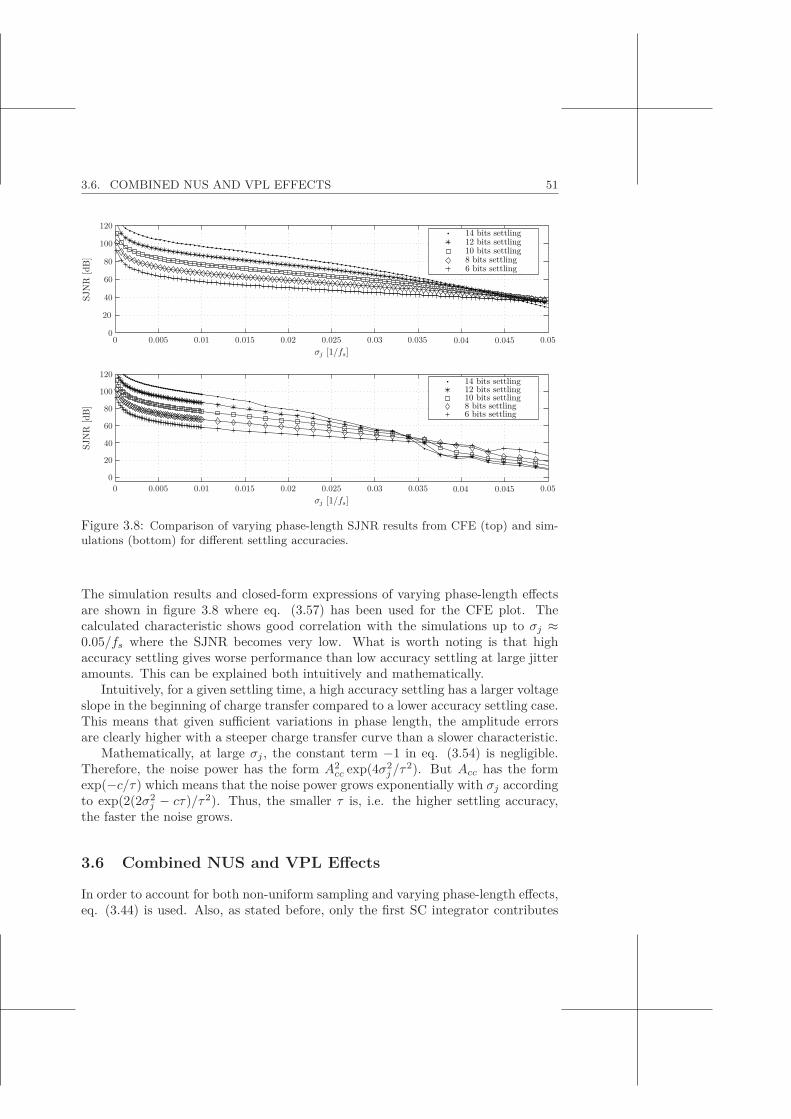
3.6. COMBINED NUS AND VPL EFFECTS 51
σj [1/fs]
SJN
R[d
B]
σj [1/fs]
SJN
R[d
B]
14 bits settling12 bits settling10 bits settling8 bits settling6 bits settling
14 bits settling12 bits settling10 bits settling8 bits settling6 bits settling
0 0.005 0.01 0.015 0.02 0.025 0.03 0.035 0.04 0.045 0.05
0 0.005 0.01 0.015 0.02 0.025 0.03 0.035 0.04 0.045 0.05
0
20
40
60
80
100
120
0
20
40
60
80
100
120
Figure 3.8: Comparison of varying phase-length SJNR results from CFE (top) and sim-ulations (bottom) for different settling accuracies.
The simulation results and closed-form expressions of varying phase-length effectsare shown in figure 3.8 where eq. (3.57) has been used for the CFE plot. Thecalculated characteristic shows good correlation with the simulations up to σj ≈0.05/fs where the SJNR becomes very low. What is worth noting is that highaccuracy settling gives worse performance than low accuracy settling at large jitteramounts. This can be explained both intuitively and mathematically.
Intuitively, for a given settling time, a high accuracy settling has a larger voltageslope in the beginning of charge transfer compared to a lower accuracy settling case.This means that given sufficient variations in phase length, the amplitude errorsare clearly higher with a steeper charge transfer curve than a slower characteristic.
Mathematically, at large σj , the constant term −1 in eq. (3.54) is negligible.Therefore, the noise power has the form A2
cc exp(4σ2j /τ
2). But Acc has the formexp(−c/τ) which means that the noise power grows exponentially with σj accordingto exp(2(2σ2
j − cτ)/τ2). Thus, the smaller τ is, i.e. the higher settling accuracy,the faster the noise grows.
3.6 Combined NUS and VPL Effects
In order to account for both non-uniform sampling and varying phase-length effects,eq. (3.44) is used. Also, as stated before, only the first SC integrator contributes

52 CHAPTER 3. JITTER EFFECTS IN SC SIGMA-DELTA ADCS
to the non-uniform sampling effects. Therefore, the other integrators will not con-tribute to any difference in impact when also NUS effects are included.
Verr,1[i] ≈ Vin[i]γ�φ1[i]
(1 −Acca[i]
)+Acc
(Vin[i] − a1Vfb[i]
)[2 − a[i] − s[i]
](3.58)
Noting the previous assumption on independent timing jitter on φ1 and φ2 it isclear that γ�
φ1[i] and a[i] are also independent. Hence, the injected error power dueto timing jitter from the first SC integrator is
Perr,1 ≈ (Aωσj)2
2+ 2A2
ccσ2inte
2σ2j /τ2
(e2σ2
j /τ2 − 1)
(3.59)
The total error power due to NUS and VPL effects at the ΣΔ modulator output isobtained as before
PNUS & VPL,out(k) ≈ (Aωσj)2
2+
+ 2A2ccσ
2inte
2σ2j /τ2
(e2σ2
j /τ2 − 1) 1fs
∫ fs/2
−fs/2
k∑j=1
∣∣JTFj(f)∣∣2df (3.60)
Figure 3.9 shows the signal-to-jitter-noise-ratio versus the jitter rms value for si-multaneous NUS and VPL effects. A lower settling accuracy clearly gives worseperformance but for accuracies higher than 10 bits, for the given input signal fre-quency fsig = 1.125 MHz, there is no extra benefit, in terms of higher SJNR, intrying to improve the settling accuracy. This is because the improvements aremasked by the NUS effects which dominate at higher settling accuracies.
3.7 Phase Overlap Effects
Phase overlap may occur if there are large amounts of jitter in the clock system.During overlap, all switches in the SC integrators are conducting as shown in figure3.10. Modelling the transistor resistances as constant and equal as before, two KVLand KCL relations can be written
Vj − i1Rt − i2Rt = 0 (3.61)i2Rt − VC1 − i3Rt = 0 (3.62)
i1 − i2 = CVC1 (3.63)i3 − CVC2 = CVC1 (3.64)
In the above relations, the previous capacitor assumption C1 = C2 = C has beendone. Since the amplifier is assumed to be ideal, the negative amplifier terminal isat zero volts potential. Hence, the voltage drops over the two switches closest tothe amplifier are equal which means they carry equal current, i3. Thus, the currentthrough C1 is twice as high as the current through C2. This can be stated as
VC1 = −2VC2 ⇒ VC1(t) = −2VC2(t) +D (3.65)

3.7. PHASE OVERLAP EFFECTS 53
σj [1/fs]
SJN
R[d
B]
σj [1/fs]
SJN
R[d
B]
[8, 10, 12, 14] bits settling
6 bits settling
[8, 10, 12, 14] bits settling
6 bits settling
0 0.005 0.01 0.015 0.02 0.025 0.03 0.035 0.04 0.045 0.05
0 0.005 0.01 0.015 0.02 0.025 0.03 0.035 0.04 0.045 0.05
0
20
40
60
80
100
120
0
20
40
60
80
100
120
Figure 3.9: Comparison of CFE (top) and simulated (bottom) SJNR from combined NUSand VPL effects for different settling accuracies.
− +
−+
+
−
i3i2i1
φ2
φ1
time
C2C1Vj
V ′j
Figure 3.10: Phase overlap situation in a single ended switched-capacitor integrator atposition j in the single stage ΣΔ chain.
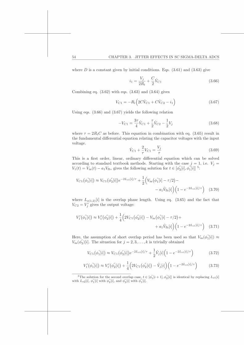
54 CHAPTER 3. JITTER EFFECTS IN SC SIGMA-DELTA ADCS
where D is a constant given by initial conditions. Eqs. (3.61) and (3.63) give
i1 =Vj
2Rt+C
2VC1 (3.66)
Combining eq. (3.62) with eqs. (3.63) and (3.64) gives
VC1 = −Rt
(2CVC1 + CVC2 − i1
)(3.67)
Using eqs. (3.66) and (3.67) yields the following relation
−VC1 =3τ4VC1 +
τ
2VC2 − 1
2Vj (3.68)
where τ = 2RtC as before. This equation in combination with eq. (3.65) result inthe fundamental differential equation relating the capacitor voltages with the inputvoltage.
VC1 +2τVC1 =
Vj
τ(3.69)
This is a first order, linear, ordinary differential equation which can be solvedaccording to standard textbook methods. Starting with the case j = 1, i.e. Vj =V1(t) = Vin(t) − a1Vfb, gives the following solution for t ∈ [φ�
2[i], φ�1[i]]
5:
VC1
(φ�
1[i]) ≈ VC1
(φ�
2[i])e−2Lo1[i]/τ +
12
(Vin
(φ�
1[i] − τ/2)−
− a1Vfb[i])(
1 − e−2Lo1[i]/τ)
(3.70)
where Lo(1,2)[i] is the overlap phase length. Using eq. (3.65) and the fact thatVC2 = V ′
j gives the output voltage:
V ′1
(φ�
1[i]) ≈ V ′
1
(φ�
2[i])
+14
(2VC1
(φ�
2[i])− Vin
(φ�
1[i] − τ/2)+
+ a1Vfb[i])(
1 − e−2Lo1[i]/τ)
(3.71)
Here, the assumption of short overlap period has been used so that Vin(φ�1[i]) ≈
Vin(φ�2)[i]. The situation for j = 2, 3, . . . , k is trivially obtained
VC1
(φ�
1[i]) ≈ VC1
(φ�
2[i])e−2Lo1[i]/τ +
12Vj [i]
(1 − e−2Lo1[i]/τ
)(3.72)
V ′1
(φ�
1[i]) ≈ V ′
1
(φ�
2[i])
+14
(2VC1
(φ�
2[i])− Vj [i]
)(1 − e−2Lo1[i]/τ
)(3.73)
5The solution for the second overlap case, t ∈ [φ�1[i + 1], φ�
2[i]] is identical by replacing Lo1[i]with Lo2[i], φ�
1[i] with φ�2[i], and φ�
2[i] with φ�1[i].
3.7. PHASE OVERLAP EFFECTS 55
In order to compare with the ideal situation, i.e. nonoverlap situation, it is firstrecognized that in such a case, ∀j,
VC1
(φ�
1[i])
= VC1
(φ�
2[i])
and V ′j
(φ�
1[i])
= V ′j
(φ�
2[i])
(3.74)
Because of the integration operation, the injected error due to overlap is measuredby the cumulative error on C1 and C2. Furthermore, it is assumed, as stated before,that only one overlap occurrence is possible per clock cycle and SC integrator. Also,effects from non-uniform sampling and varying phase-length are neglected. Withoutlosing generality, the overlap is assumed to be between the falling edge of φ1 andthe rising edge of φ2 during clock cycle i. Hence, the error may be written
Verr,1[i] =[VC1
(φ�
2[i])− VC1
(φ�
1[i])︸ ︷︷ ︸
error on C1
]+
[V ′
1
(φ�
2[i])− V ′
1
(φ�
1[i])︸ ︷︷ ︸
error on C2
](3.75)
Expanding this relation by using eqs. (3.70)-(3.73) yields the following:
Verr,1[i] =(1
2VC1
(φ�
2[i])− 1
4Vin
(φ�
2[i] − τ/2)
+14a1Vfb[i]
)(1 − e−2Lo1[i]/τ
)(3.76)
If full settling is assumed, i.e. τ is very small, it is possible to write the first termin (3.76) as
VC1
(φ�
2[i])
= Vin(φ�
2[i] − τ)− a1Vfb[i] ≈ Vin
(φ�
1[i] − τ/2)− a1Vfb[i] (3.77)
Therefore, by neglecting memory effects in the ΣΔ modulator, the jitter-inducederror due to phase overlap in the first SC integrator is
Verr,1[i] ≈ V1[i]4
(1 − e−2Lo1[i]/τ
)(3.78)
An equivalent deduction for the other SC integrators give the same result for allintegrators
Verr,j[i] ≈ Vj [i]4
(1 − e−2Lo1[i]/τ
)(3.79)
The average power of the phase overlap error injected in each switched-capacitorintegrator is given by
Perr,j ≈ σ2int16
V{
1 − e−2Lo1[i]/τ}
(3.80)
≈ σ2int16
(E{e−4Lo1[i]/τ
}− E2
{e−2Lo1[i]/τ
})(3.81)
The statistical properties of the measure of overlap, ε(1,2)[i], defined in section 3.3 ineq. (3.23) are not the properties of Lo(1,2)[i] since they do not take the probabilityof overlap into account and hence cannot be used directly for power calculations.
56 CHAPTER 3. JITTER EFFECTS IN SC SIGMA-DELTA ADCS
However, by defining the overlap lengths according to the following relation it ispossible to deduce the phase overlap probability dependent error power.
Lo(1,2)[i] ≡ f(ε(1,2)[i]
)=
{0 , if ε(1,2)[i] ≤ 0ε(1,2)[i] , if ε(1,2)[i] > 0
(3.82)
With this definition, the fact that only a small number of clock cycles have phaseoverlap can be taken into account. The following relations describe the definitionsof the terms in eq. (3.81).
f4(ε1[i]
) ≡ e−4Lo1[i]/τ = e−4f(ε1[i])/τ =
{1 , if ε1[i] ≤ 0e−4ε1[i]/τ , if ε1[i] > 0
(3.83)
f2(ε1[i]
) ≡ e−2Lo1[i]/τ = e−2f(ε1[i])/τ =
{1 , if ε1[i] ≤ 0e−2ε1[i]/τ , if ε1[i] > 0
(3.84)
Thus it is now possible to calculate the expectation values needed in eq. (3.81).
E{e−4Lo1[i]/τ
}=
1σ√
2π
∫ ∞
−∞f4(x) exp
[−(x+ (0.5 − dφ1)T
σ√
2
)2]dx
= Φ( aσ
)+ exp
(8σ2 + 4aττ2
)[1 − Φ
(4σ2 + aτ
στ
)](3.85)
E{e−2Lo1[i]/τ
}=
1σ√
2π
∫ ∞
−∞f2(x) exp
[−(x+ (0.5 − dc)T
σ√
2
)2]dx
= Φ( aσ
)+ exp
(2σ2 + 2aττ2
)[1 − Φ
(2σ2 + aτ
στ
)](3.86)
Here, the standard deviation σ = 2σj and a = (0.5 − dφ1)T . Furthermore, Φ(x) isdefined as
Φ(x) =1√2π
∫ x
−∞e−t2/2dt (3.87)
For the case 2 overlap, dφ1 is simply substituted with dφ2. With the above relationsit is now trivial to deduce the injected error power due to phase overlap at each SCintegrator.
Perr,j ≈ σ2int16
[Φ( aσ
)− Φ2
( aσ
)+ e(8σ2+4aτ)/τ2
(1 − Φ
(4σ2 + aτ
στ
))−
−e(4σ2+4aτ)/τ2(
1−Φ(2σ2 + aτ
στ
))2
−2Φ( aσ
)e(2σ2+2aτ)/τ2
(1−Φ
(2σ2 + aτ
στ
))](3.88)

3.8. SUMMARY 57
The total error power at the ΣΔ modulator output is obtained as in the previoussections
PPO,out(k) ≈ Perr,jfs
∫ fs/2
−fs/2
k∑j=1
∣∣JTFj(f)∣∣2df (3.89)
Often, the values of a, σ, and τ are such that (4σ2 + aτ)/στ and (2σ2 + aτ)/στare large, e.g. when dφ1 = 25%, 20 bits settling, and σ = 0.1/fs. In this case, it istypically not possible to calculate the error power with eq. (3.88) due to numericalreasons. Instead, the following approximation can be made:
1 − Φ(x) ≈ 1x√
2πe−x2/2 (3.90)
Thus, an approximation to the injected error power due to phase overlap at eachSC integrator is
Perr,j ≈ σ2int16
[Φ( aσ
)− Φ2
( aσ
)+
1√2πe−a2/2σ2 στ
4σ2 + aτ−
− 12πe−a2/σ2
( στ
2σ2 + aτ
)2
− 2Φ( aσ
) 1√2πe−a2/2σ2
( στ
2σ2 + aτ
)](3.91)
Figure 3.11 shows a comparison between the expression given above and the simu-lation results, at a settling accuracy of 14 bits, for a second order single stage ΣΔmodulator, indicating close correspondence. The flat region in the left part of theplot is when the probability of overlap is low enough for phase overlap to not occurduring the given simulation time.
3.8 Summary
Timing jitter is increasing in magnitude with faster sampling frequencies and theeffects of jitter increase with higher signal frequencies. At some point in this dualincrease in frequency, the timing jitter effects will overtake the traditionally dom-inant effects of quantization noise. This point is expected to be reached at anearly stage specifically for Sigma-Delta modulators which suppress the effects ofquantization noise within the signal bandwidth.
The three jitter effects, non-uniform sampling, varying phase-length, and phaseoverlap have been presented in an isolated way in order to reach an understand-ing of their individual contributions to the noise impact. The novel closed-formexpressions show good agreement with the simulation results. However, a realisticsituation naturally incorporates all three effects simultaneously. In this respect, itis interesting to compare the three effects to determine if one is dominant over theother. Figure 3.12 shows such a comparison in terms of noise power for various sig-nal frequencies and settling accuracies. From this figure it is clear that if a sufficientsettling accuracy is maintained, non-uniform sampling effects will be dominant as

58 CHAPTER 3. JITTER EFFECTS IN SC SIGMA-DELTA ADCS
σj [1/fs]
SJN
R[d
B]
simulationCFE
0.02 0.04 0.06 0.08 0.1 0.12 0.14 0.16 0.18 0.20
20
40
60
80
100
120
140
160
180
Figure 3.11: Comparison of CFE (·) and simulated (−) SJNR from phase overlap effectsfor a settling accuracy of 14 bits.
σj [1/fs]
Per
r,ou
t[d
B]
VPL 14 bits settlingVPL 10 bits settlingVPL 6 bits settlingPO 14 bits settlingPO 10 bits settlingPO 6 bits settlingNUS fsig = 3 MHzNUS fsig = 1 MHzNUS fsig = 100 kHz
0 0.005 0.01 0.015 0.02 0.025 0.03 0.035 0.04 0.045 0.05-220
-200
-180
-160
-140
-120
-100
-80
-60
-40
Figure 3.12: Comparison between noise power of the three types of timing jitter effects,non-uniform sampling (NUS), varying phase-lengths (VPL), and phase overlap (PO).
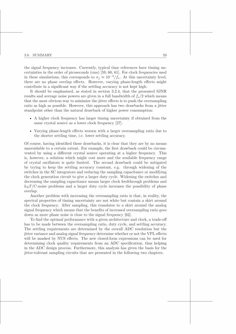
3.8. SUMMARY 59
the signal frequency increases. Currently, typical time references have timing un-certainties in the order of picoseconds (rms) [59, 60, 61]. For clock frequencies usedin these simulations, this corresponds to σj ≈ 10−4/fs. At this uncertainty level,there are no phase overlap effects. However, varying phase-length effects mightcontribute in a significant way if the settling accuracy is not kept high.
It should be emphasized, as stated in section 3.2.4, that the presented SJNRresults and average noise powers are given in a full bandwidth of fs/2 which meansthat the most obvious way to minimize the jitter effects is to push the oversamplingratio as high as possible. However, this approach has two drawbacks from a jitterstandpoint other than the natural drawback of higher power consumption:
• A higher clock frequency has larger timing uncertainty if obtained from thesame crystal source as a lower clock frequency [27].
• Varying phase-length effects worsen with a larger oversampling ratio due tothe shorter settling time, i.e. lower settling accuracy.
Of course, having identified these drawbacks, it is clear that they are by no meansunavoidable to a certain extent. For example, the first drawback could be circum-vented by using a different crystal source operating at a higher frequency. Thisis, however, a solution which might cost more and the available frequency rangeof crystal oscillators is quite limited. The second drawback could be mitigatedby trying to keep the settling accuracy constant, e.g. through widening of theswitches in the SC integrators and reducing the sampling capacitance or modifyingthe clock generation circuit to give a larger duty cycle. Widening the switches anddecreasing the sampling capacitance means larger clock feedthrough problems andkBT/C-noise problems and a larger duty cycle increases the possibility of phaseoverlap.
Another problem with increasing the oversampling ratio is that, in reality, thespectral properties of timing uncertainty are not white but contain a skirt aroundthe clock frequency. After sampling, this translates to a skirt around the analogsignal frequency which means that the benefits of increased oversampling ratio goesdown as more phase noise is close to the signal frequency [62].
To find the optimal performance with a given architecture and clock, a trade-offhas to be made between the oversampling ratio, duty cycle, and settling accuracy.The settling requirements are determined by the overall ADC resolution but thejitter variance and analog signal frequency determine whether or not the VPL effectswill be masked by NUS effects. The new closed-form expressions can be used fordetermining clock quality requirements from an ADC specification, thus helpingin the ADC design process. Furthermore, this analysis has given the basis for thejitter-tolerant sampling circuits that are presented in the following two chapters.


Chapter 4The Parallel Sampler
4.1 Introduction
The previous chapter presented a description of the effects a nonideal time referencehas on the output of a single stage switched-capacitor Sigma-Delta modulator. Thenon-uniform sampling (NUS) effect was shown to be the most detrimental of thethree presented effects as signal frequencies become larger in the pursuit of SoftwareRadio. For reference, the impact of non-uniform sampling effects on the output isrepeated from eq. (3.32):
SJNRNUS ≈ 1(2πfσj)2
(4.1)
The signal frequency cannot be altered since it is determined by the transceiverarchitecture and application. Hence, this chapter will mainly focus on presentingand analysing a sampling topology which experiences a reduced timing uncertainty.The basis of this chapter is from [1] and [3] in the list of publications.
4.2 The Parallel Sampler Idea
A well-known technique to reduce the variance of a stochastic variable is averaging.This is used for example to reduce random variations in process parameters throughlayout techniques such as interdigitization [63]. The averaging technique is basedon a fundamental theorem in statistics named the Central Limit Theorem. Thistheorem states the following [64]:
Central Limit Theorem. Given n independent identically distributed (i.i.d.) sto-chastic variables, xi, with mean m and standard deviation σ. Then, the distributionof
x =1n
(x1 + x2 + · · · + xn
)(4.2)
61
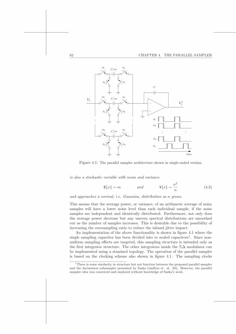
62 CHAPTER 4. THE PARALLEL SAMPLER
... ...
+
−
... ...
φ1
φ1φa
φa
φa
φa
φa
φa
φ2
φ2
φm
φm
C
C/m
C/m
C/m
φ1
time
φa
φ2
φm
V1V ′
1
Figure 4.1: The parallel sampler architecture shown in single-ended version.
is also a stochastic variable with mean and variance
E{x} = m and V{x} =σ2
n(4.3)
and approaches a normal, i.e. Gaussian, distribution as n grows.
This means that the average power, or variance, of an arithmetic average of noisysamples will have a lower noise level than each individual sample, if the noisesamples are independent and identically distributed. Furthermore, not only doesthe average power decrease but any uneven spectral distributions are smoothedout as the number of samples increases. This is desirable due to the possibility ofincreasing the oversampling ratio to reduce the inband jitter impact.
An implementation of the above functionality is shown in figure 4.1 where thesingle sampling capacitor has been divided into m scaled capacitors1. Since non-uniform sampling effects are targeted, this sampling structure is intended only asthe first integrator structure. The other integrators inside the ΣΔ modulator canbe implemented using a standard topology. The operation of the parallel sampleris based on the clocking scheme also shown in figure 4.1. The sampling clocks
1There is some similarity in structure but not function between the proposed parallel samplerand the decimation subsampler presented by Saska Lindfors et. al. [65]. However, the parallelsampler idea was conceived and analysed without knowledge of Saska’s work.

4.2. THE PARALLEL SAMPLER IDEA 63
{φ1, φ2, . . . , φm} are ideally identical but have independent jitter properties. Theaccumulation clock φa operates as in a standard switched-capacitor integrator, al-lowing the sampled charge to be transferred onto the accumulation capacitor. As-suming full settling and no phase overlap between sampling phase and accumulationphase, the relation describing the voltage change over the accumulation capacitorat each clock cycle is given by
ΔV ′1 [i] =
1m
m−1∑k=0
Vin(iT + γ�
φ(k+1)[i])
(4.4)
where the constant phase shift −ωτ from eq. (3.6) in section 3.2.2 has been ne-glected since it is a constant term and doesn’t affect the jitter impact. Furthermore,the feedback term −a1Vfb[i] has also been neglected since it is a piecewise constantsignal which doesn’t contribute to the jitter effects. Assuming, as before, thatγ�
φ(k+1)[i] is small for all i and k it is straightforward to make a Taylor expansionaround t = iT to obtain
ΔV ′1 [i] ≈ 1
m
m−1∑k=0
Vin[i] + γ�φ(k+1)[i]Vin[i] (4.5)
Simplifying this relation by noting that only the stochastic term is dependent on kgives
ΔV ′1 [i] ≈ Vin[i] + VNUS[i] (4.6)
where VNUS[i] is the injected error due to timing jitter and is given by
VNUS[i] ≈ Vin[i]m
m−1∑k=0
γ�φ(k+1)[i] (4.7)
From this relation it is clear that the average noise power in the full fs/2 bandwidthis
PNUS,out ≈ V 2in[i]
1m2
V
{m−1∑k=0
γ�φ(k+1)[i]
}(4.8)
If the timing uncertainties are independent, V{∑xi} =∑
V{xi}. If they are alsoidentically distributed with standard deviation σj , the average noise power becomes
PNUS,out ≈ V 2in[i]
σ2j
m=
(Aωσj)2
2m(4.9)
given Vin(t) = A sin(ωt). Figure 4.2 shows the decrease of noise power at the ΣΔmodulator output as a function of the number of sampling capacitors, m, in theideal case of i.i.d. jitter on {φ1, φ2, . . . , φm}. The translation to extra bit resolutionhas been done with eq. (2.6) in section 2.3. Also, the reference level for the relativeordinate scale is set to 0 dB for m = 1. Naturally, using many sampling capacitorsalso has several drawbacks, some of which are
64 CHAPTER 4. THE PARALLEL SAMPLER
Number of capacitors m
Rel
ativ
eer
ror
powe
r[d
B]
4 capacitors ⇒ 1 bit extra
16 capacitors ⇒ 2 bits extra
64 capacitors ⇒ 3 bits extra
0 10 20 30 40 50 60 70 80 90 100-20
-18
-16
-14
-12
-10
-8
-6
-4
-2
0
Figure 4.2: Optimal parallel sampler performance with ideal devices and i.i.d. jitter onthe sampling phases.
• Larger uncertainty of the individual capacitor charge due to smaller size stem-ming from clock feedthrough and charge injection. This can be mitigated byscaling the MOS transistor switches down with the capacitors.
• Larger area occupied by interconnects and switches creating higher probabil-ity of crosstalk.
• Difficulty in having enough statistically independent and synchronized clocksources. Individual PLLs for each clock signal occupies a lot of space andconsumes a lot of extra power.
To see how the noise power is distributed in frequency, the power spectrum can beobtained with the Wiener-Khinchin theorem [30, 66], briefly stated in section 1.4.
Wiener-Khinchin Theorem. The power spectrum S(f) of a wide-sense station-ary, i.e. weakly stationary, continuous stochastic process x(t) is the Fourier trans-form of its autocorrelation function rx(τ).
rx(τ) = C{x(t+ τ), x(t)
}= E
{x(t+ τ)x(t)
}− E{x(t+ τ)
}E{x(t)
}(4.10)
S(f) = F{rx(τ)} =∫ ∞
−∞rx(τ)e−j2πfτdτ (4.11)
Hence, the autocorrelation function of the injected error in eq. (4.7) is
rNUS[i, p] = C{VNUS[i+ p], VNUS[i]
}(4.12)
= E{VNUS[i+ p]VNUS[i]
}− E{VNUS[i+ p]
}E{VNUS[i]
}(4.13)
4.2. THE PARALLEL SAMPLER IDEA 65
Assuming the elements in the sequence {γ�φ(k+1)}, k = 0, 1, . . . ,m− 1 are indepen-
dent with zero mean and standard deviation σj , it is clear that
E{VNUS[i]
}= E
{Vin[i]m
m−1∑k=0
γ�φ(k+1)[i]
}=Vin[i]m
m−1∑k=0
E{γ�
φ(k+1)[i]}
= 0 (4.14)
Therefore
rNUS[i, p] = E{VNUS[i+ p]VNUS[i]
}(4.15)
= E
{Vin[i+ p]Vin[i]
m2
m−1∑k1=0
γ�φ(k1+1)[i+ p]
m−1∑k2=0
γ�φ(k2+1)[i]
}(4.16)
=Vin[i+ p]Vin[i]
m2
m−1∑k1=0
m−1∑k2=0
E{γ�
φ(k1+1)[i+ p]γ�φ(k2+1)[i]
}(4.17)
Since it was assumed that the jitter has zero mean
E{γ�φ(k1+1)[i+ p]γ�
φ(k2+1)[i]} =
{σ2
j , if k1 = k2 and p = 00 , otherwise
(4.18)
Thus
rNUS[i, p] =
{σ2
j V2
in[i]/m , if p = 00 , otherwise
(4.19)
Clearly, rNUS[i, p] is not wide-sense stationary since the autocorrelation depends oni. However, if Vin[i] = A sin(ωiT ) it is possible to approximate the autocorrelationfunction with a time average.
rNUS[i, p] =
{(Aωσj)2 cos2(ωiT )/m , if p = 00 , otherwise
(4.20)
rNUS[p] =
{(Aωσj)2/2m , if p = 00 , otherwise
(4.21)
This approximation is wide-sense stationary and as such it is possible to calculatethe power spectrum by means of time-discrete Fourier transformation.
SNUS(fd) = Ftd{rNUS[p]
}=
∞∑p=−∞
rNUS[p]e−j2πfdp (4.22)
where fd = f/fs ∈ [−0.5, 0.5]. Since rNUS[p] = 0 for all p �= 0, this is equivalent toan impulse function which means the power spectrum is constant for all frequencies.
SNUS(fd) =(Aωσj)2
2m(4.23)
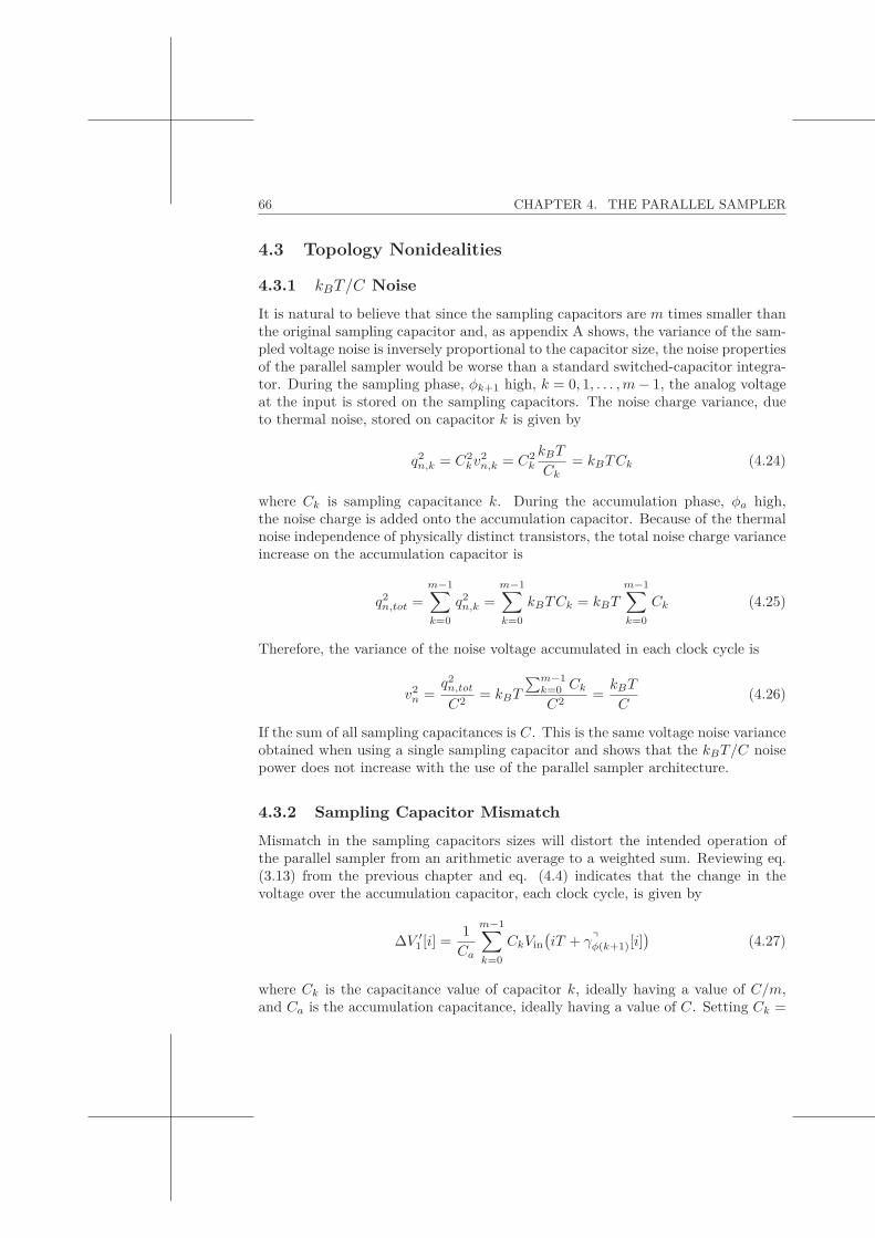
66 CHAPTER 4. THE PARALLEL SAMPLER
4.3 Topology Nonidealities
4.3.1 kBT/C Noise
It is natural to believe that since the sampling capacitors are m times smaller thanthe original sampling capacitor and, as appendix A shows, the variance of the sam-pled voltage noise is inversely proportional to the capacitor size, the noise propertiesof the parallel sampler would be worse than a standard switched-capacitor integra-tor. During the sampling phase, φk+1 high, k = 0, 1, . . . ,m− 1, the analog voltageat the input is stored on the sampling capacitors. The noise charge variance, dueto thermal noise, stored on capacitor k is given by
q2n,k = C2kv
2n,k = C2
k
kBT
Ck= kBTCk (4.24)
where Ck is sampling capacitance k. During the accumulation phase, φa high,the noise charge is added onto the accumulation capacitor. Because of the thermalnoise independence of physically distinct transistors, the total noise charge varianceincrease on the accumulation capacitor is
q2n,tot =m−1∑k=0
q2n,k =m−1∑k=0
kBTCk = kBT
m−1∑k=0
Ck (4.25)
Therefore, the variance of the noise voltage accumulated in each clock cycle is
v2n =
q2n,tot
C2= kBT
∑m−1k=0 Ck
C2=kBT
C(4.26)
If the sum of all sampling capacitances is C. This is the same voltage noise varianceobtained when using a single sampling capacitor and shows that the kBT/C noisepower does not increase with the use of the parallel sampler architecture.
4.3.2 Sampling Capacitor Mismatch
Mismatch in the sampling capacitors sizes will distort the intended operation ofthe parallel sampler from an arithmetic average to a weighted sum. Reviewing eq.(3.13) from the previous chapter and eq. (4.4) indicates that the change in thevoltage over the accumulation capacitor, each clock cycle, is given by
ΔV ′1 [i] =
1Ca
m−1∑k=0
CkVin(iT + γ�
φ(k+1)[i])
(4.27)
where Ck is the capacitance value of capacitor k, ideally having a value of C/m,and Ca is the accumulation capacitance, ideally having a value of C. Setting Ck =
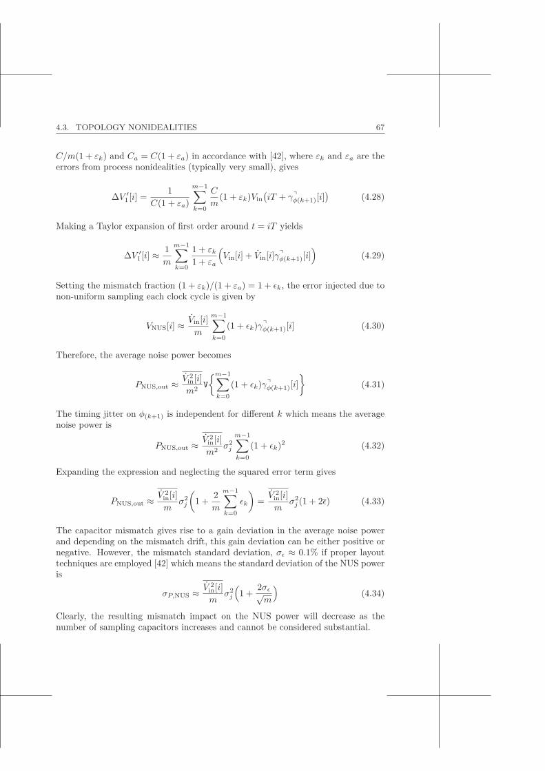
4.3. TOPOLOGY NONIDEALITIES 67
C/m(1 + εk) and Ca = C(1 + εa) in accordance with [42], where εk and εa are theerrors from process nonidealities (typically very small), gives
ΔV ′1 [i] =
1C(1 + εa)
m−1∑k=0
C
m(1 + εk)Vin
(iT + γ�
φ(k+1)[i])
(4.28)
Making a Taylor expansion of first order around t = iT yields
ΔV ′1 [i] ≈ 1
m
m−1∑k=0
1 + εk
1 + εa
(Vin[i] + Vin[i]γ�
φ(k+1)[i])
(4.29)
Setting the mismatch fraction (1 + εk)/(1 + εa) = 1 + εk, the error injected due tonon-uniform sampling each clock cycle is given by
VNUS[i] ≈ Vin[i]m
m−1∑k=0
(1 + εk)γ�φ(k+1)[i] (4.30)
Therefore, the average noise power becomes
PNUS,out ≈ V 2in[i]m2
V
{m−1∑k=0
(1 + εk)γ�φ(k+1)[i]
}(4.31)
The timing jitter on φ(k+1) is independent for different k which means the averagenoise power is
PNUS,out ≈ V 2in[i]m2
σ2j
m−1∑k=0
(1 + εk)2 (4.32)
Expanding the expression and neglecting the squared error term gives
PNUS,out ≈ V 2in[i]m
σ2j
(1 +
2m
m−1∑k=0
εk
)=V 2
in[i]m
σ2j (1 + 2ε) (4.33)
The capacitor mismatch gives rise to a gain deviation in the average noise powerand depending on the mismatch drift, this gain deviation can be either positive ornegative. However, the mismatch standard deviation, σε ≈ 0.1% if proper layouttechniques are employed [42] which means the standard deviation of the NUS poweris
σP,NUS ≈ V 2in[i]m
σ2j
(1 +
2σε√m
)(4.34)
Clearly, the resulting mismatch impact on the NUS power will decrease as thenumber of sampling capacitors increases and cannot be considered substantial.
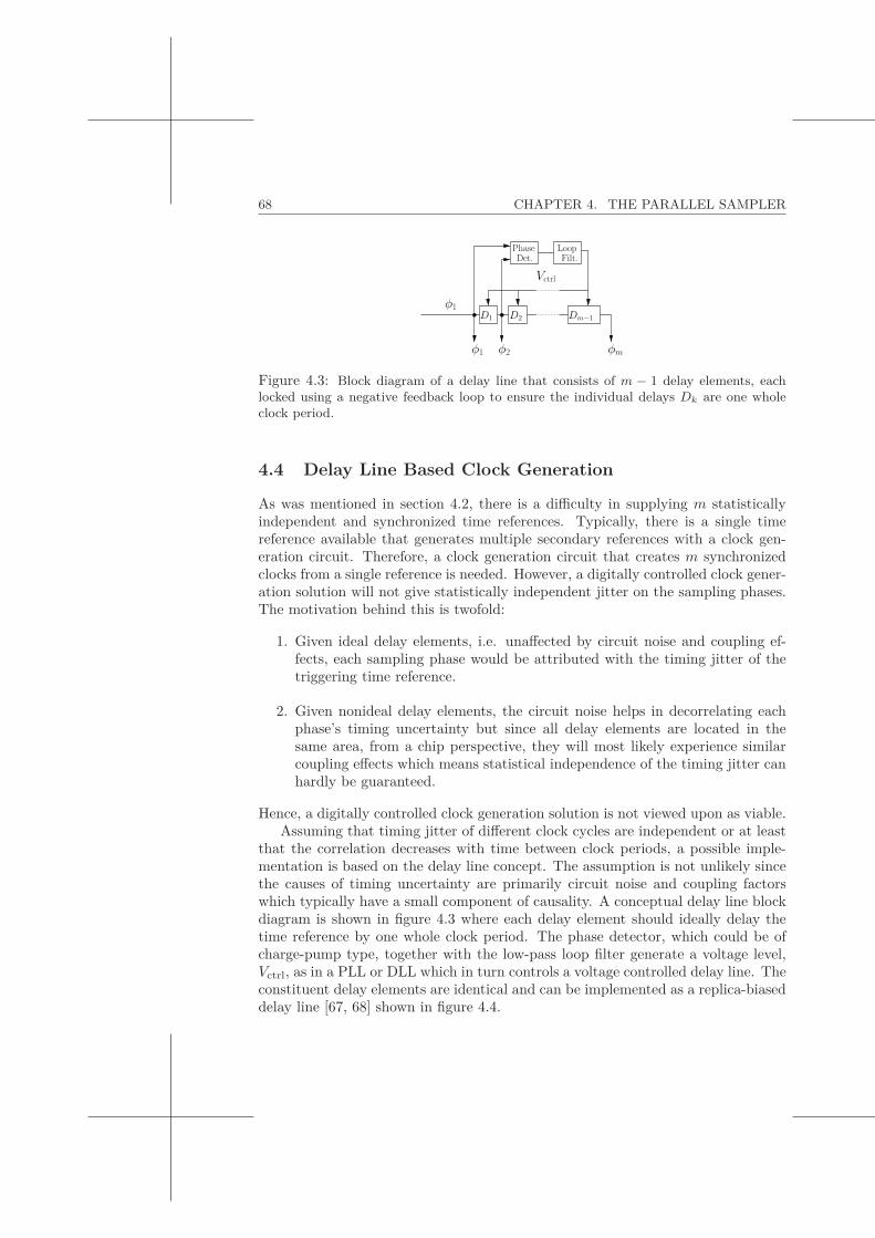
68 CHAPTER 4. THE PARALLEL SAMPLER
φmφ2φ1
φ1Dm−1D2D1
Vctrl
Filt.Loop
Det.Phase
Figure 4.3: Block diagram of a delay line that consists of m − 1 delay elements, eachlocked using a negative feedback loop to ensure the individual delays Dk are one wholeclock period.
4.4 Delay Line Based Clock Generation
As was mentioned in section 4.2, there is a difficulty in supplying m statisticallyindependent and synchronized time references. Typically, there is a single timereference available that generates multiple secondary references with a clock gen-eration circuit. Therefore, a clock generation circuit that creates m synchronizedclocks from a single reference is needed. However, a digitally controlled clock gener-ation solution will not give statistically independent jitter on the sampling phases.The motivation behind this is twofold:
1. Given ideal delay elements, i.e. unaffected by circuit noise and coupling ef-fects, each sampling phase would be attributed with the timing jitter of thetriggering time reference.
2. Given nonideal delay elements, the circuit noise helps in decorrelating eachphase’s timing uncertainty but since all delay elements are located in thesame area, from a chip perspective, they will most likely experience similarcoupling effects which means statistical independence of the timing jitter canhardly be guaranteed.
Hence, a digitally controlled clock generation solution is not viewed upon as viable.Assuming that timing jitter of different clock cycles are independent or at least
that the correlation decreases with time between clock periods, a possible imple-mentation is based on the delay line concept. The assumption is not unlikely sincethe causes of timing uncertainty are primarily circuit noise and coupling factorswhich typically have a small component of causality. A conceptual delay line blockdiagram is shown in figure 4.3 where each delay element should ideally delay thetime reference by one whole clock period. The phase detector, which could be ofcharge-pump type, together with the low-pass loop filter generate a voltage level,Vctrl, as in a PLL or DLL which in turn controls a voltage controlled delay line. Theconstituent delay elements are identical and can be implemented as a replica-biaseddelay line [67, 68] shown in figure 4.4.
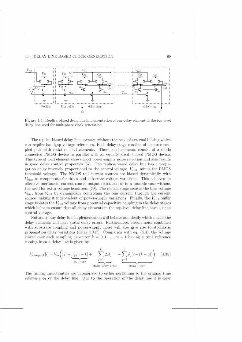
4.4. DELAY LINE BASED CLOCK GENERATION 69
−
+
Vdd
Vctrl
Replica Vctrl buffer delay stage
VddVdd
VddVdd
+Vc
Vbias
in+
in−out+out−
Vdd
V ′ctrl
φ1
Vbias
delay stage
in+ in−out+out−
Vdd
V ′ctrl
Vdd
φ2
Figure 4.4: Replica-biased delay line implementation of one delay element in the top-leveldelay line used for multiphase clock generation.
The replica-biased delay line operates without the need of external biasing whichcan require bandgap voltage references. Each delay stage consists of a source cou-pled pair with resistive load elements. These load elements consist of a diodeconnected PMOS device in parallel with an equally sized, biased PMOS device.This type of load element shows good power-supply noise rejection and also resultsin good delay control properties [67]. The replica-biased delay line has a propa-gation delay inversely proportional to the control voltage, Vctrl, minus the PMOSthreshold voltage. The NMOS tail current sources are biased dynamically withVbias to compensate for drain and substrate voltage variations. This achieves aneffective increase in current source output resistance as in a cascode case withoutthe need for extra voltage headroom [69]. The replica stage creates the bias voltageVbias from Vctrl by dynamically controlling the bias current through the currentsource making it independent of power-supply variations. Finally, the Vctrl bufferstage isolates the Vctrl voltage from potential capacitive coupling in the delay stageswhich helps to ensure that all delay elements in the top-level delay line have a cleancontrol voltage.
Naturally, any delay line implementation will behave nonideally which means thedelay elements will have static delay errors. Furthermore, circuit noise combinedwith substrate coupling and power-supply noise will also give rise to stochasticpropagation delay variations (delay jitter). Comparing with eq. (4.4), the voltagestored over each sampling capacitor k = 0, 1, . . . ,m − 1 having a time referencecoming from a delay line is given by
Vsample,k[i] = Vin
(iT + γ�
φ1[i− k]︸ ︷︷ ︸φ1 jitter
+k∑
j=1
Δdj
︸ ︷︷ ︸static delay error
+k∑
q=1
δq[i− (k − q)]
︸ ︷︷ ︸delay jitter
)(4.35)
The timing uncertainties are categorized to either pertaining to the original timereference φ1 or the delay line. Due to the operation of the delay line it is clear

70 CHAPTER 4. THE PARALLEL SAMPLER
that φ(k+1) is a copy of φ1 that has been delayed k clock cycles. Furthermore, eachdelay element is associated with a static delay error, Δdk for k = 1, 2, . . . ,m − 1which represents a constant shift of the propagation delay. Finally, any dynamicpropagation delay variations are assumed to be stochastic and are bundled into adelay element dependent and time dependent term δk[i].
Assuming the static delay errors can be neglected and the stochastic time vari-ations in eq. (4.35) are sufficiently small, a good approximation to the sampledvoltage is given by a Taylor expansion around t = iT :
Vsample,k[i] ≈ Vin[i] + Vin[i](γ�
φ1[i− k] +k∑
q=1
δp[i− (k − q)])
(4.36)
4.5 A Jitter-Free Delay Line
Starting with analysing the case of a jitter-free delay line, δk[i] = 0 for all k, i,means the non-uniform sampling error at the output of the parallel sampler is
VNUS[i] ≈ Vin[i]m
m−1∑k=0
γ�φ1[i− k] (4.37)
The power spectrum is obtained as before by forming the autocorrelation function
rNUS[i, p] = C{VNUS[i+ p], VNUS[i]
}= E
{VNUS[i+ p]VNUS[i]
}(4.38)
Therefore
rNUS[i, p] = E
{Vin[i+ p]Vin[i]
m2
m−1∑k1=0
γ�φ1[i+ p− k1]
m−1∑k2=0
γ�φ1[i− k2]
}(4.39)
=Vin[i+ p]Vin[i]
m2
m−1∑k1=0
m−1∑k2=0
E{γ�
φ1[i+ p− k1]γ�φ1[i− k2]
}(4.40)
By remembering the previous assumption of inter-cycle independence, the autocor-relation becomes
rNUS[i, p] =
{(m− |p|)σ2
j Vin[i+ p]Vin[i]/m2 , if |p| ≤ m− 10 , otherwise
(4.41)
Clearly, the autocorrelation function is not wide-sense stationary which means anapproximation needs to be made. Following the example in eqs. (4.20) and (4.21)it is possible to write
rNUS[i, p] =
{(m− |p|)(Aωσj)2 cos
((i+ p)ωT
)cos
(ωiT
)/m2 , if |p| ≤ m− 1
0 , otherwise(4.42)
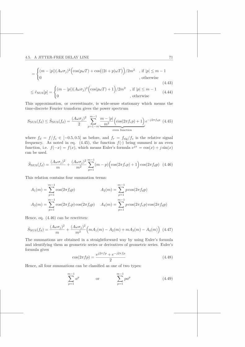
4.5. A JITTER-FREE DELAY LINE 71
=
{(m− |p|)(Aωσj)2
(cos(pωT ) + cos
((2i+ p)ωT
))/2m2 , if |p| ≤ m− 1
0 , otherwise(4.43)
≤ rNUS[p] =
{(m− |p|)(Aωσj)2
(cos(pωT ) + 1
)/2m2 , if |p| ≤ m− 1
0 , otherwise(4.44)
This approximation, or overestimate, is wide-sense stationary which means thetime-discrete Fourier transform gives the power spectrum
SNUS(fd) ≤ SNUS(fd) =(Aωσj)2
2
m−1∑p=1−m
m− |p|m2
(cos(2πfrp) + 1
)︸ ︷︷ ︸
even function
e−j2πfdp (4.45)
where fd = f/fs ∈ [−0.5, 0.5] as before, and fr = fsig/fs is the relative signalfrequency. As noted in eq. (4.45), the function f(·) being summed is an evenfunction, i.e. f(−x) = f(x), which means Euler’s formula ejx = cos(x) + j sin(x)can be used.
SNUS(fd) =(Aωσj)2
m+
(Aωσj)2
m2
m−1∑p=1
(m− p)(cos(2πfrp) + 1
)cos(2πfdp) (4.46)
This relation contains four summation terms:
A1(m) =m−1∑p=1
cos(2πfdp) A2(m) =m−1∑p=1
p cos(2πfdp)
A3(m) =m−1∑p=1
cos(2πfrp) cos(2πfdp) A4(m) =m−1∑p=1
p cos(2πfrp) cos(2πfdp)
Hence, eq. (4.46) can be rewritten:
SNUS(fd) =(Aωσj)2
m+
(Aωσj)2
m2
(mA1(m) −A2(m) +mA3(m) −A4(m)
)(4.47)
The summations are obtained in a straightforward way by using Euler’s formulaand identifying them as geometric series or derivatives of geometric series. Euler’sformula gives
cos(2πfp) =ej2πfp + e−j2πfp
2(4.48)
Hence, all four summations can be classified as one of two types:
m−1∑p=1
ap orm−1∑p=1
pap (4.49)
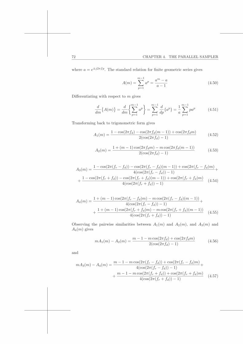
72 CHAPTER 4. THE PARALLEL SAMPLER
where a = e±j2πfp. The standard relation for finite geometric series gives
A(m) =m−1∑p=1
ap =am − a
a− 1(4.50)
Differentiating with respect to m gives
d
dm
{A(m)
}=
d
dm
{m−1∑p=1
ap
}=
m−1∑p=1
d
dp{ap} =
1a
m−1∑p=1
pap (4.51)
Transforming back to trigonometric form gives
A1(m) =1 − cos(2πfd) − cos(2πfd(m− 1)) + cos(2πfdm)
2(cos(2πfd) − 1)(4.52)
A2(m) =1 + (m− 1) cos(2πfdm) −m cos(2πfd(m− 1))
2(cos(2πfd) − 1)(4.53)
A3(m) =1 − cos(2π(fr − fd)) − cos(2π(fr − fd)(m− 1)) + cos(2π(fr − fd)m)
4(cos(2π(fr − fd)) − 1)+
+1 − cos(2π(fr + fd)) − cos(2π(fr + fd)(m− 1)) + cos(2π(fr + fd)m)
4(cos(2π(fr + fd)) − 1)(4.54)
A4(m) =1 + (m− 1) cos(2π(fr − fd)m) −m cos(2π(fr − fd)(m− 1))
4(cos(2π(fr − fd)) − 1)+
+1 + (m− 1) cos(2π(fr + fd)m) −m cos(2π(fr + fd)(m− 1))
4(cos(2π(fr + fd)) − 1)(4.55)
Observing the pairwise similarities between A1(m) and A2(m), and A3(m) andA4(m) gives
mA1(m) −A2(m) =m− 1 −m cos(2πfd) + cos(2πfdm)
2(cos(2πfd) − 1)(4.56)
and
mA3(m) −A4(m) =m− 1 −m cos(2π(fr − fd)) + cos(2π(fr − fd)m)
4(cos(2π(fr − fd)) − 1)+
+m− 1 −m cos(2π(fr + fd)) + cos(2π(fr + fd)m)
4(cos(2π(fr + fd)) − 1)(4.57)
4.5. A JITTER-FREE DELAY LINE 73
fd
m
SN
US
[dB]
fr = 0.01
fd
mS
NU
S[d
B]
fr = 0.1
fd
m
SN
US
[dB]
fr = 0.2
fd
m
SN
US
[dB]
fr = 0.4
00.1
0.20.3
0.40.5
00.1
0.20.3
0.40.5
00.1
0.20.3
0.40.5
00.1
0.20.3
0.40.5
1020
3040
50
1020
3040
50
1020
3040
50
1020
3040
50
-40
-200
20
-40
-200
20
-40
-200
20
-40
-200
20
Figure 4.5: Relative power spectrum of NUS noise from a delay line based parallel samplerwith perfect delay elements.
By using the fundamental trigonometric relation cos(2x) = 1 − 2 sin2(x) and sim-plifying, the power spectrum estimate for a jitter-free delay line is obtained.
SNUS(fd) =(Aωσj)2
2m2
[sin2(π(fr − fd)m)2 sin2(π(fr − fd))
+sin2(π(fr + fd)m)2 sin2(π(fr + fd))
+sin2(πfdm)sin2(πfd)
](4.58)
Figure 4.5 shows the relative power spectrum for varying number of sampling capac-itorsm = {1, 2, . . . , 50} and four different signal frequencies fr = {0.01, 0.1, 0.2, 0.4}.The reference level 0 dB has been set to the ideal case as described by eq. (4.23)when all the clocks’ timing uncertainties are independent and also cycle-to-cycleindependent for each individual clock. The difference of 3 dB especially visible atm = 1 is due to the two different approaches in calculating the power spectrum(approximation by time average vs. overestimate). The power spectrum showsamplification of the noise level around the signal frequency fr as the number ofsampling capacitors m increases. Furthermore, the width of the noise skirt aroundthe signal decreases as m increases which can be intuitively explained by the factthat the autocorrelation remains above zero for a longer period of time which cor-responds to a narrower peak in frequency domain.
To see how the total noise power depends on the number of sampling capacitorsit is noted that V{x} = rx[0]. Hence, setting p = 0 in eq. (4.42) and making a time

74 CHAPTER 4. THE PARALLEL SAMPLER
average gives an equivalent result as the ideal case in eq. (4.23):
PNUS ≈ (Aωσj)2
2m(4.59)
This means the full bandwidth noise suppression remains unchanged compared tothe ideal case. However, since the bandwidth of the signal is much smaller in reality,the inband NUS noise suppression decreases as m increases. To see the bandwidthdependent NUS noise power, it is observed that the inband noise power is given by
PNUS(fB) ≈ 1fs
∫ fB
−fB
SNUS(fd)df (4.60)
Furthermore, the ideal inband NUS noise power is obtained from eq. (4.23)
PNUS,ideal(fB) ≈ 1fs
∫ fB
−fB
SNUS(fd)df =(Aωσj)2
2m2fB
fs(4.61)
The relative bandwidth dependent NUS noise power is then formed by
Pr,NUS(fB) =PNUS(fB)
2PNUS,ideal(fB)(4.62)
This relation shows how the inband noise power compares with the ideal inbandnoise power and gives a measure of how the power distribution distorts as the num-ber of sampling capacitors increases and the signal bandwidth varies. The reasonfor dividing by two is simply because the ideal noise power has been obtained byapproximation by a time average whereas the delay line based power spectrum hasbeen calculated using an upper bound. The mismatch between the two approachesis a factor of two. Figure 4.6 shows how the relative inband NUS noise power dropsas the signal bandwidth approaches fs/2 for the same four signal frequencies fr asbefore. It is clear that the noise skirt around the signal frequency has a large effecton the inband noise power which means that a larger oversampling ratio decreasesthe benefit of using the delay line clock generation approach.
4.6 A Noisy Delay Line
In reality, the situation is not as has been analyzed in the previous section. Thedelay line also adds timing uncertainty to the delayed clock signals. As the clock,φ1, goes through more delay elements, it is natural to presume that the timinguncertainty of the delayed clocks {φk} grows as k grows. Equation (4.36) gives thenon-uniform sampling voltage error injected in clock cycle i:
VNUS[i] ≈ Vin[i]m
m−1∑k=0
γ�φ1[i− k]
︸ ︷︷ ︸Bγ [i]
+Vin[i]m
m−1∑k=0
k∑q=1
δq[i− (k − q)]
︸ ︷︷ ︸Bδ[i]
(4.63)
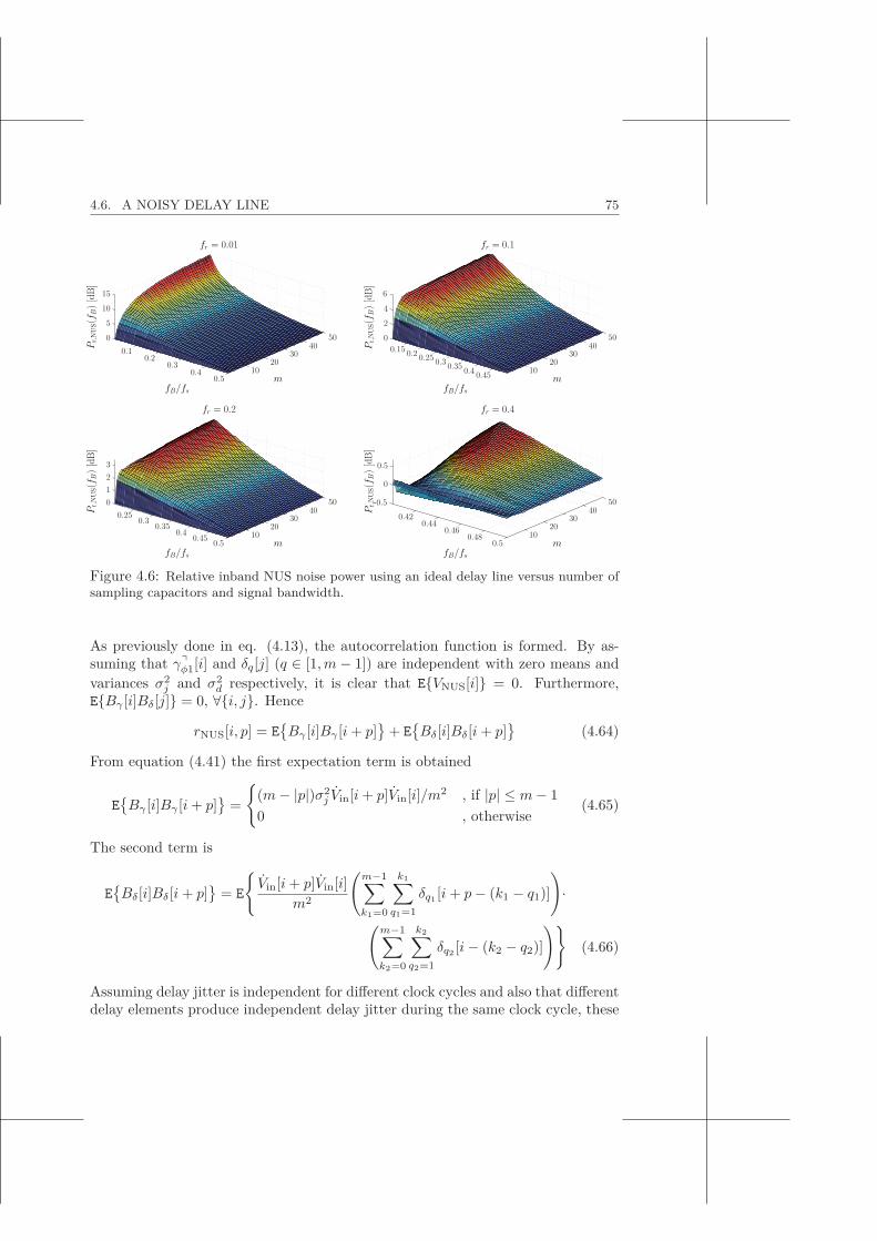
4.6. A NOISY DELAY LINE 75
fB/fs
m
Pr,N
US(
f B)
[dB]
fr = 0.01
fB/fs
mP
r,NU
S(f B
)[d
B]
fr = 0.1
fB/fs
m
Pr,N
US(
f B)
[dB]
fr = 0.2
fB/fs
m
Pr,N
US(
f B)
[dB]
fr = 0.4
0.420.44
0.460.48
0.5
0.25 0.3 0.350.4 0.45 0.5
0.15 0.2 0.25 0.3 0.35 0.4 0.45
0.10.2
0.30.4
0.5
1020
3040
50
1020
3040
50
1020
3040
50
1020
3040
50
-0.5
0
0.5
0123
024
6
05
1015
Figure 4.6: Relative inband NUS noise power using an ideal delay line versus number ofsampling capacitors and signal bandwidth.
As previously done in eq. (4.13), the autocorrelation function is formed. By as-suming that γ�
φ1[i] and δq[j] (q ∈ [1,m− 1]) are independent with zero means andvariances σ2
j and σ2d respectively, it is clear that E{VNUS[i]} = 0. Furthermore,
E{Bγ [i]Bδ[j]} = 0, ∀{i, j}. Hence
rNUS[i, p] = E{Bγ [i]Bγ [i+ p]
}+ E
{Bδ[i]Bδ[i+ p]
}(4.64)
From equation (4.41) the first expectation term is obtained
E{Bγ [i]Bγ [i+ p]
}=
{(m− |p|)σ2
j Vin[i+ p]Vin[i]/m2 , if |p| ≤ m− 10 , otherwise
(4.65)
The second term is
E{Bδ[i]Bδ[i+ p]
}= E
{Vin[i+ p]Vin[i]
m2
(m−1∑k1=0
k1∑q1=1
δq1 [i+ p− (k1 − q1)]
)·
(m−1∑k2=0
k2∑q2=1
δq2 [i− (k2 − q2)]
)}(4.66)
Assuming delay jitter is independent for different clock cycles and also that differentdelay elements produce independent delay jitter during the same clock cycle, these
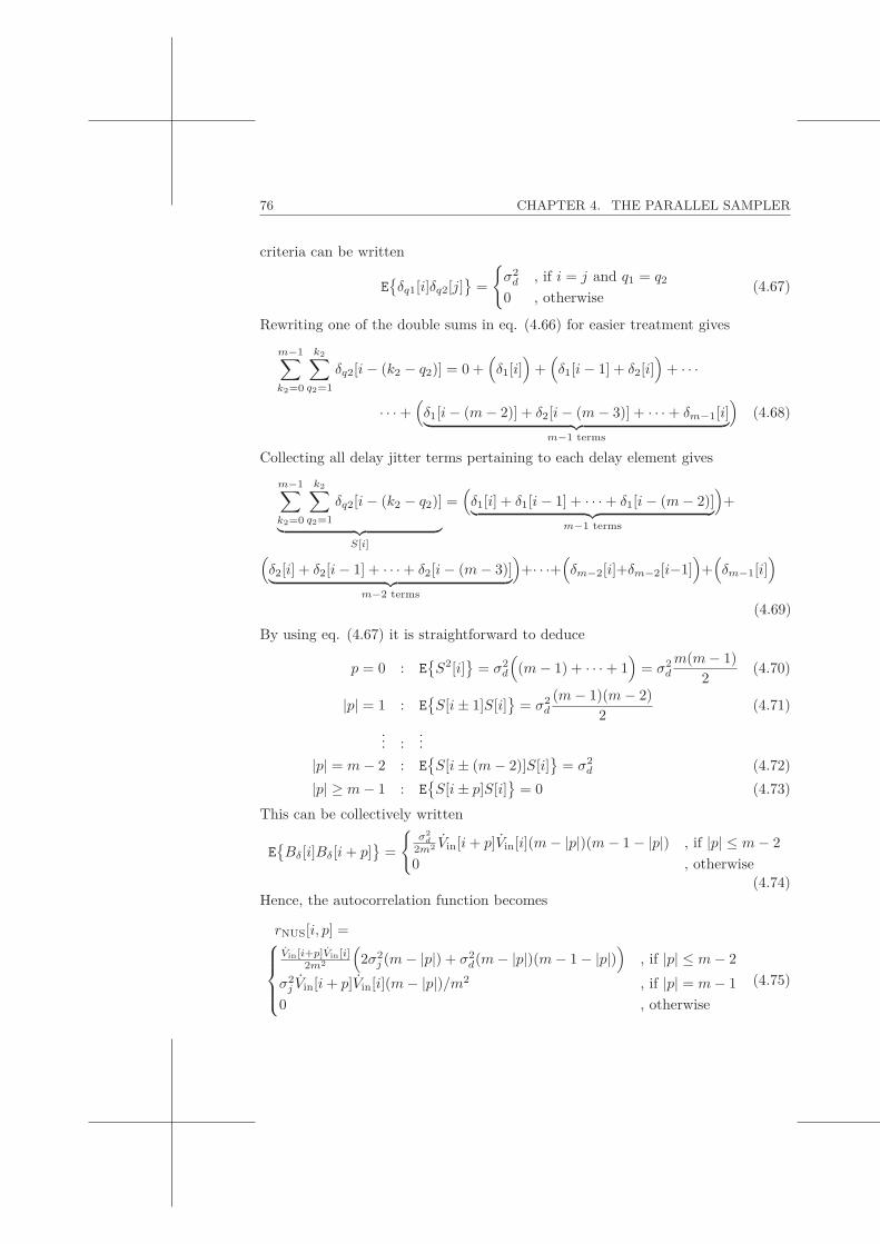
76 CHAPTER 4. THE PARALLEL SAMPLER
criteria can be written
E{δq1[i]δq2[j]
}=
{σ2
d , if i = j and q1 = q2
0 , otherwise(4.67)
Rewriting one of the double sums in eq. (4.66) for easier treatment gives
m−1∑k2=0
k2∑q2=1
δq2[i− (k2 − q2)] = 0 +(δ1[i]
)+
(δ1[i− 1] + δ2[i]
)+ · · ·
· · · +(δ1[i− (m− 2)] + δ2[i− (m− 3)] + · · · + δm−1[i]︸ ︷︷ ︸
m−1 terms
)(4.68)
Collecting all delay jitter terms pertaining to each delay element givesm−1∑k2=0
k2∑q2=1
δq2[i− (k2 − q2)]
︸ ︷︷ ︸S[i]
=(δ1[i] + δ1[i− 1] + · · · + δ1[i− (m− 2)]︸ ︷︷ ︸
m−1 terms
)+
(δ2[i] + δ2[i− 1] + · · · + δ2[i− (m− 3)]︸ ︷︷ ︸
m−2 terms
)+· · ·+
(δm−2[i]+δm−2[i−1]
)+(δm−1[i]
)(4.69)
By using eq. (4.67) it is straightforward to deduce
p = 0 : E{S2[i]
}= σ2
d
((m− 1) + · · · + 1
)= σ2
d
m(m− 1)2
(4.70)
|p| = 1 : E{S[i± 1]S[i]
}= σ2
d
(m− 1)(m− 2)2
(4.71)
... :...
|p| = m− 2 : E{S[i± (m− 2)]S[i]
}= σ2
d (4.72)|p| ≥ m− 1 : E
{S[i± p]S[i]
}= 0 (4.73)
This can be collectively written
E{Bδ[i]Bδ[i+ p]
}=
{σ2
d
2m2 Vin[i+ p]Vin[i](m− |p|)(m− 1 − |p|) , if |p| ≤ m− 20 , otherwise
(4.74)Hence, the autocorrelation function becomes
rNUS[i, p] =⎧⎪⎪⎨⎪⎪⎩
Vin[i+p]Vin[i]2m2
(2σ2
j (m− |p|) + σ2d(m− |p|)(m− 1 − |p|)
), if |p| ≤ m− 2
σ2j Vin[i+ p]Vin[i](m− |p|)/m2 , if |p| = m− 1
0 , otherwise(4.75)

4.6. A NOISY DELAY LINE 77
By, once again, setting Vin[i] = A sin(2πfri), with fr = fsig/fs, the autocorrelationis overestimated to give wide-sense stationarity.
rNUS[p] =
⎧⎪⎪⎪⎪⎪⎨⎪⎪⎪⎪⎪⎩
(Aω)2
4m2
(cos(2πfrp) + 1
)(2σ2
j (m− |p|)++σ2
d(m− |p|)(m− 1 − |p|))
, if |p| ≤ m− 2
(Aωσj)2(cos(2πfrp) + 1
)(m− |p|)/2m2 , if |p| = m− 1
0 , otherwise
(4.76)
It is clear that rNUS[p] is an even function which means that the power spectrumcan be written as
SNUS(fd) =(Aωm
)2(mσ2
j +σ2
d
2m(m− 1)
)+
(Aωm
)2 m−1∑p=1
(cos(2πfrp) + 1
)(σ2
j (m− p) +σ2
d
2(m− p)(m− 1 − p)
)cos(2πfdp)
(4.77)
Figure 4.7 shows the power spectrum for a signal frequency of fr = 0.05 and fourdelay jitter magnitudes σd = {0, 0.33, 0.66, 1}σj as the number of sampling capac-itors is varied. The 0 dB level has again been chosen according to eq. (4.23). Asthe delay jitter increases, the suppression of non-uniform sampling effects decreasesand the noise spectrum also gets smoothed out. The delay line plays an impor-tant role in the suppression level obtainable and increasing the number of samplingcapacitors doesn’t necessarily mean a decrease of the NUS noise power. This isevident from calculating the average noise power, rNUS[0], for m > 1:
PNUS ≈ (Aω)2(σ2
j
m+σ2
d
2
(1 − 1
m
))(4.78)
Comparing with twice the ideal full band noise power given by eq. (4.23) shows thatthe crossover point for worse than ideal suppression lies at σd = 1.4σj . Figure 4.8shows the relation between NUS noise power, number of sampling capacitors andfraction between delay jitter and clock jitter. Since the noise power is not evenlydistributed in frequency but more focused around the signal frequency, the delay jit-ter crossover point is substantially lower than 1.4σj when considering only inbandjitter-induced noise. The actual crossover point depends on both the signal fre-quency, bandwidth, and sampling frequency. This will be shown in the simulationssection 4.8. An example of this can be shown by observing the inband SJNR whenvarying the oversampling ratio. For this example, fr = 0.00078 (fsig = 750 kHz,fs = 96 MHz), m = {2, 4, 8, 16, 32, 64}, σd = {0.01, 0.1, 0.3, 1}σj , and σj = 0.1/fs.Figure 4.9 shows that the best NUS noise suppression is obtained for low oversam-pling ratios which means wideband applications are natural targets of the parallelsampling technique.
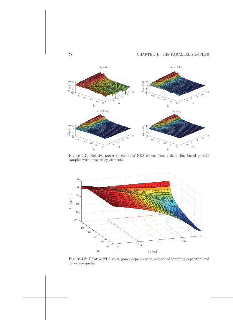
78 CHAPTER 4. THE PARALLEL SAMPLER
fd
m
SN
US
[dB]
σd = 0
fd
m
SN
US
[dB]
σd = 0.33σj
fd
m
SN
US
[dB]
σd = 0.66σj
fd
m
SN
US
[dB]
σd = σj
00.1
0.20.3
0.40.5
00.1
0.20.3
0.40.5
00.1
0.20.3
0.40.5
00.1
0.20.3
0.40.5
1020
3040
50
1020
3040
50
1020
3040
50
1020
3040
50
-40-20
020
-40-20
020
-40-20
020
-40-20
020
Figure 4.7: Relative power spectrum of NUS effects from a delay line based parallelsampler with noisy delay elements.
σd [σj ]m
Pr,
NU
S[d
B]
00.5
11.5
2
1020
3040
50
-20
-15
-10
-5
0
5
Figure 4.8: Relative NUS noise power depending on number of sampling capacitors anddelay line quality.
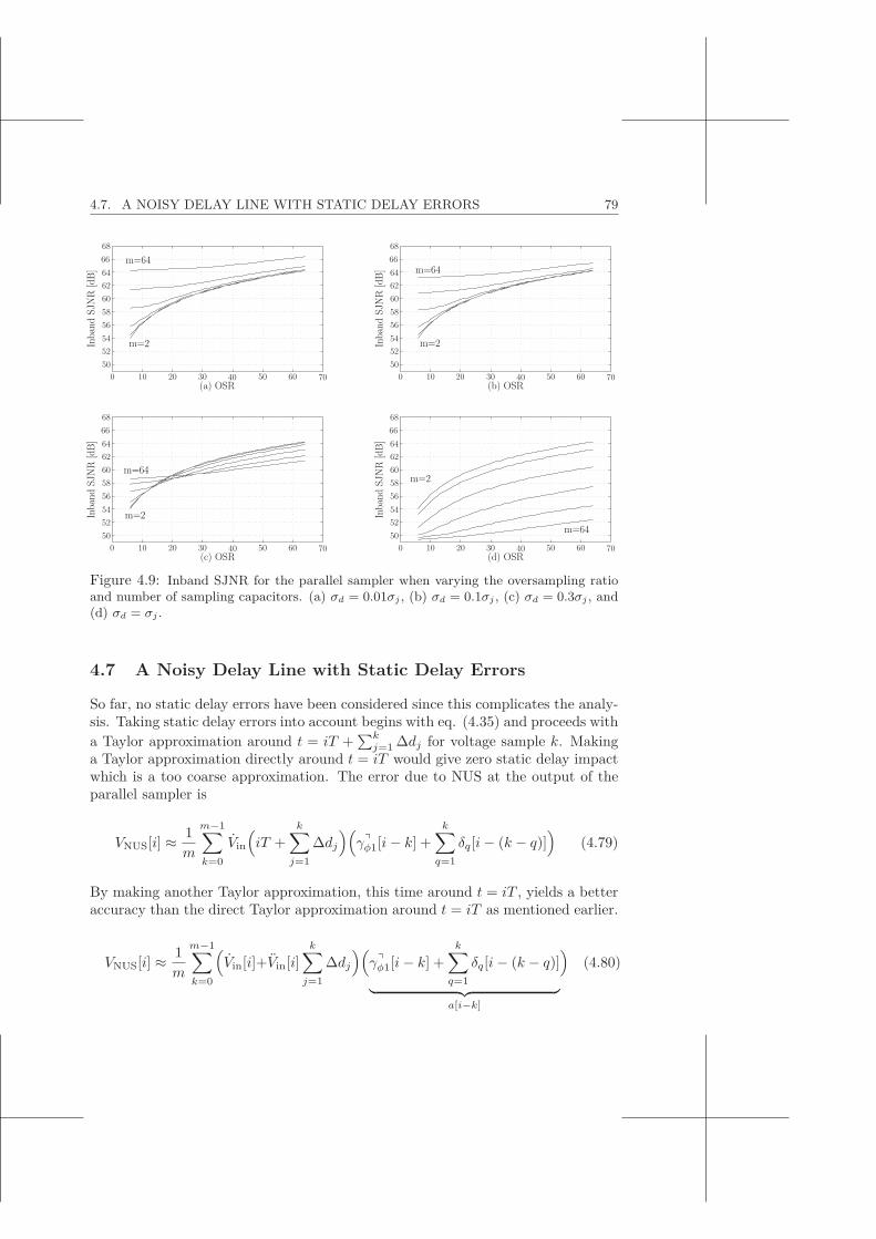
4.7. A NOISY DELAY LINE WITH STATIC DELAY ERRORS 79
(a) OSR
Inba
ndSJ
NR
[dB]
(b) OSRIn
band
SJN
R[d
B]
(c) OSR
Inba
ndSJ
NR
[dB]
(d) OSR
Inba
ndSJ
NR
[dB]
m=64
m=2
m=2
m=64m=64
m=64
m=2
m=2
0 10 20 30 40 50 60 700 10 20 30 40 50 60 70
0 10 20 30 40 50 60 700 10 20 30 40 50 60 70
50525456586062646668
50525456586062646668
50525456586062646668
50525456586062646668
Figure 4.9: Inband SJNR for the parallel sampler when varying the oversampling ratioand number of sampling capacitors. (a) σd = 0.01σj , (b) σd = 0.1σj , (c) σd = 0.3σj , and(d) σd = σj .
4.7 A Noisy Delay Line with Static Delay Errors
So far, no static delay errors have been considered since this complicates the analy-sis. Taking static delay errors into account begins with eq. (4.35) and proceeds witha Taylor approximation around t = iT +
∑kj=1 Δdj for voltage sample k. Making
a Taylor approximation directly around t = iT would give zero static delay impactwhich is a too coarse approximation. The error due to NUS at the output of theparallel sampler is
VNUS[i] ≈ 1m
m−1∑k=0
Vin
(iT +
k∑j=1
Δdj
)(γ�
φ1[i− k] +k∑
q=1
δq[i− (k − q)])
(4.79)
By making another Taylor approximation, this time around t = iT , yields a betteraccuracy than the direct Taylor approximation around t = iT as mentioned earlier.
VNUS[i] ≈ 1m
m−1∑k=0
(Vin[i]+Vin[i]
k∑j=1
Δdj
)(γ�
φ1[i− k] +k∑
q=1
δq[i− (k − q)]
︸ ︷︷ ︸a[i−k]
)(4.80)
80 CHAPTER 4. THE PARALLEL SAMPLER
This approximation is only good if ω∑k
j=1 Δdj 1 for all k which is quite likelysince the sampling frequency is at least one order of magnitude greater than thesignal bandwidth and the static delay errors shouldn’t be more than a few percentof the entire clock period to ensure the phase overlap probability remains low. Theaverage NUS error power is obtained using the variance operator
PNUS = V{VNUS[i]
}= E
{V 2
NUS[i]}− E2
{VNUS[i]
}︸ ︷︷ ︸=0
(4.81)
The second term is zero given zero mean stochastic variables, γ and δ, as assumedin the previous section. Hence the average power is given by the second momentof the error voltage. By writing the input signal Vin[i] = A sin(ωiT ) as before, thevoltage error becomes
VNUS[i] ≈ Aω
mcos(ωiT )
(m−1∑k=0
a[i− k])− Aω2
msin(ωiT )
(m−1∑k=0
a[i− k]k∑
j=1
Δdj
)(4.82)
The fundamental trigonometric identity a cos(x) + b sin(x) =√a2 + b2 sin(x + ϕ)
gives an opportunity to overestimate the voltage error in the following way.
V 2NUS[i] ≤
(Aωm
)2[(m−1∑
k=0
a[i− k])2
+ ω2
(m−1∑k=0
a[i− k]k∑
j=1
Δdj
︸ ︷︷ ︸x[i,k]
)2]
(4.83)
The multinomial formula enables the expansion of the above relation which meansthe average power becomes
PNUS ≤(Aωm
)2[E
{ ∑k0+···+km−1=2
2!k0! · · · km−1!
a[i]k0 · · · a[i− (m− 1]]km−1
}+
+ ω2E
{ ∑k0+···+km−1=2
2!k0! · · · km−1!
x[i, 0]k0 · · ·x[i,m− 1]km−1
}](4.84)
Using the linearity property of the expectation operator means
PNUS ≤(Aωm
)2[ ∑
k0+···+km−1=2
2!k0! · · · km−1!
E
{m−1∏p=0
a[i− p]kp
}+
+ ω2∑
k0+···+km−1=2
2!k0! · · · km−1!
E
{m−1∏p=0
x[i, p]kp
}](4.85)
Clearly, since {k0, k1, . . . , km−1} are non-negative integers such that their sum is 2,kp = {0, 1, 2} are the only possible values. Starting with the first expectation term

4.7. A NOISY DELAY LINE WITH STATIC DELAY ERRORS 81
gives
E
{m−1∏p=0
a[i− p]kp
}= E
{m−1∏p=0
(γ�
φ1[i− p] +p∑
q=1
δq[i− (p− q)])kp
}(4.86)
The individual factors within the expectation operator are independent given theearlier assumptions in the previous section. Hence,
E
{m−1∏p=0
a[i− p]kp
}=
m−1∏p=0
E
{(γ�
φ1[i− p] +p∑
q=1
δq[i− (p− q)])kp
}(4.87)
For arbitrary p1 and p2, such that kp1 = kp2 = 1, all other kp = 0 which meansthe product in eq. (4.87) is zero. Hence, then only combination of kp variablesgiving a non-zero product is kp1 = 2 for an arbitrary p1 and kp = 0 for all other p.Therefore, the noise power becomes
PNUS ≤(Aωm
)2[
m−1∑p=0
E{a[i− p]2
}+
+ ω2∑
k0+···+km−1=2
2!k0! · · · km−1!
E
{m−1∏p=0
x[i, p]kp
}](4.88)
Expanding the first term in eq. (4.88) gives
E{a[i− p]2
}= E
{(γ�
φ1[i− p] +p∑
q=1
δq[i− (p− q)])2
}= σ2
j + pσ2d (4.89)
The second expectation term in eq. (4.88) is
E
{m−1∏p=0
x[i, p]kp
}= E
{m−1∏p=0
a[i− p]kp
( p∑j=1
Δdj
)kp}
(4.90)
It was earlier determined that a[i − p1] and a[i − p2] are independent for p1 �= p2
and the extra factors of static delay errors do not affect this. Hence,
E
{m−1∏p=0
x[i, p]kp
}=
m−1∏p=0
E{a[i− p]kp
}( p∑j=1
Δdj
)kp
(4.91)
As previously deduced, the product in eq. (4.91) is zero if kp = 1 for an arbitraryp. Therefore, the only combination of kp variables giving a non-zero product iskp1 = 2 for an arbitrary p1 and kp = 0 for all other p. Therefore, the noise powerbecomes
PNUS ≤(Aωm
)2[
m−1∑p=0
(σ2
j + pσ2d
)+ ω2
m−1∑p=0
(σ2
j + pσ2d
)( p∑j=1
Δdj
︸ ︷︷ ︸D[p]
)2]
(4.92)
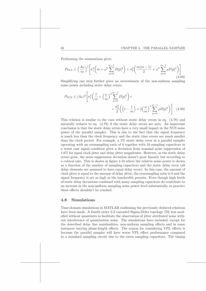
82 CHAPTER 4. THE PARALLEL SAMPLER
Performing the summations gives
PNUS ≤(Aωm
)2[σ2
j
(m+ ω2
m−1∑p=0
D[p]2)
+ σ2d
(m(m− 1)
2+ ω2
m−1∑p=0
pD[p]2)](4.93)
Simplifying one step further gives an overestimate of the non-uniform samplingnoise power including static delay errors.
PNUS ≤ (Aω)2[σ2
j
(1m
+( ωm
)2 m−1∑p=0
D[p]2)
+
+σ2
d
2
((1 − 1
m
)+ 2
( ωm
)2 m−1∑p=0
pD[p]2)]
(4.94)
This relation is similar to the case without static delay errors in eq. (4.78) andnaturally reduces to eq. (4.78) if the static delay errors are zero. An importantconclusion is that the static delay errors have a very small impact in the NUS noisepower of the parallel sampler. This is due to the fact that the signal frequencyis much less than the clock frequency and the static time errors are much smallerthan the clock period. For example, a 5% static delay error in a parallel sampleroperating with an oversampling ratio of 8 together with 10 sampling capacitors ina worst case signal condition gives a deviation from nominal noise suppression of1.6% for equal clock jitter and delay jitter magnitudes. However, as the static delayerrors grow, the noise suppression deviation doesn’t grow linearly but according toa cubical rate. This is shown in figure 4.10 where the relative noise power is shownas a function of the number of sampling capacitors and the static delay error (alldelay elements are assumed to have equal delay error). In this case, the amount ofclock jitter is equal to the amount of delay jitter, the oversampling ratio is 8 and thesignal frequency is set as high as the bandwidth permits. Even though high levelsof static delay deviations combined with many sampling capacitors do contribute toan increase in the non-uniform sampling noise power level substantially, in practicethese effects shouldn’t be reached.
4.8 Simulations
Time-domain simulations in MATLAB confirming the previously deduced relationshave been made. A fourth order 2-2 cascaded Sigma-Delta topology [70] was mod-elled without quantizers to facilitate the observation of jitter attributed noise with-out interference of quantization noise. The simulations have included, except forthe described delay line nonidealities, non-uniform sampling effects and in someinstances varying phase-length effects. The reason for considering VPL effects isbecause the parallel sampler will have worse VPL effect performance comparedto a standard sampling circuit due to the extra sampling capacitors. The timing

4.8. SIMULATIONS 83
mΔd [1/fs]
Rel
ativ
eN
oise
Powe
r
0 10 20 30 4050
0
0.05
0.11
1.5
2
2.5
3
Figure 4.10: NUS noise power relative to the nominal case as function of static delayerrors and number of capacitors.
uncertainties were modelled as independent stochastic variables having Gaussiandistributions with zero mean. The effects of NUS and VPL were modelled as comingfrom separate timing uncertainties with individual standard deviations σj = σNUSand σVPL respectively although they in reality are stemming from the same timinguncertainty. Moreover, the signal amplitude has been A = 0.1 V with a frequencyfsig = 1.125 MHz. The clock signals have had a duty cycle of 25%, frequencyfs = 96 MHz and an oversampling ratio of 16. Static delay errors were also takenfrom a set with Gaussian distribution having standard deviation σΔd and zero mean.Phase overlaps were not considered since this phenomenon only appears when usinghigh duty-cycle clocks and/or clocks with very poor jitter characteristics. Neitherof these situations were deemed relevant for this analysis.
A power spectral density plot of the ΣΔ output for different numbers of inputcapacitors is shown in figure 4.11 and also varying levels of delay jitter but nottaking static delay errors into account. This plot clearly shows how the noisebecomes more colored as the number of sampling capacitors increases. Moreover,the suppression is bandwidth dependent although the total NUS noise power fallsas 1/m. There is a high degree of similarity between the simulation results shownin figure 4.11 and the closed-form expression (CFE) results shown in figures 4.5 and4.7.
Further simulation results deal with how the inband SJNR is affected by havingdifferent number of sampling capacitors versus different amounts of delay jitterand static delay errors. The delay jitter was chosen according to four levels, σd =
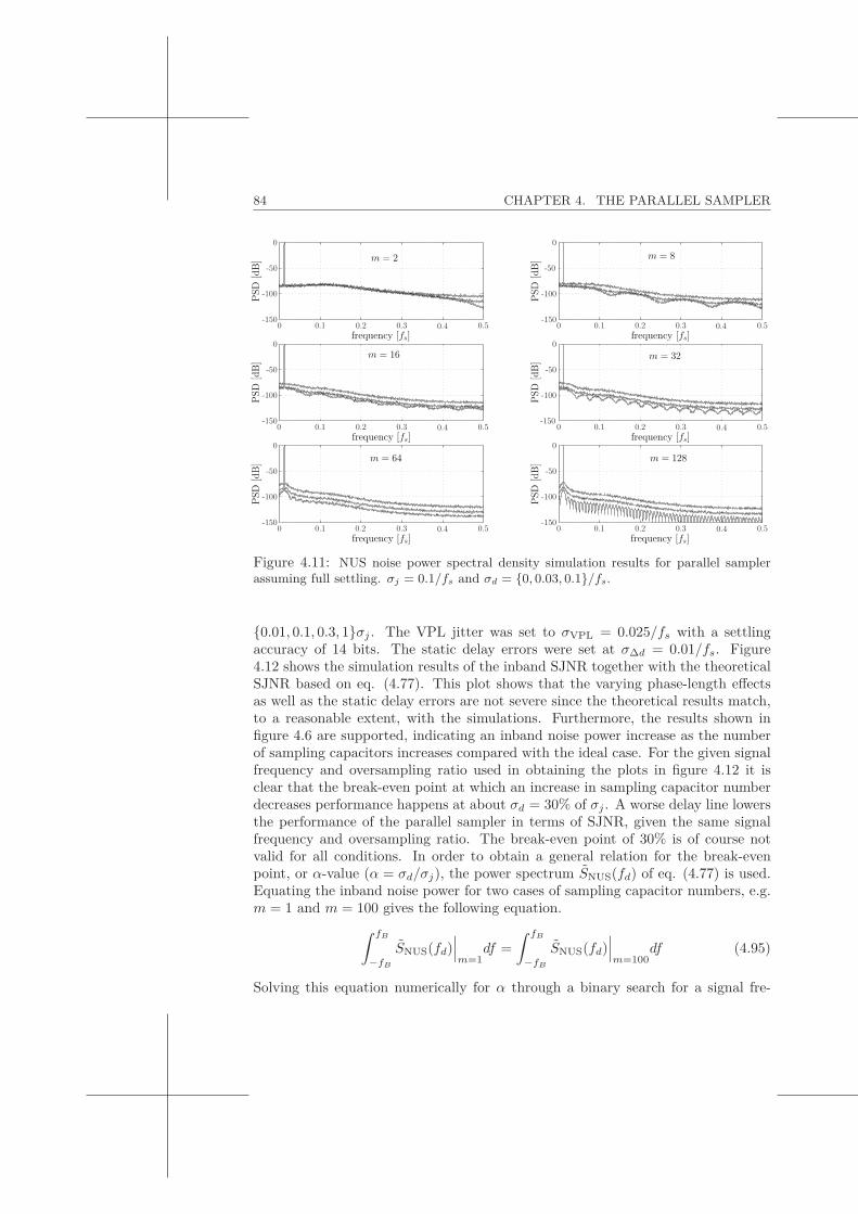
84 CHAPTER 4. THE PARALLEL SAMPLER
frequency [fs]
PSD
[dB]
frequency [fs]
PSD
[dB]
frequency [fs]
PSD
[dB]
frequency [fs]
PSD
[dB]
frequency [fs]
PSD
[dB]
frequency [fs]PS
D[d
B]
m = 2 m = 8
m = 16 m = 32
m = 64 m = 128
0 0.1 0.2 0.3 0.4 0.50 0.1 0.2 0.3 0.4 0.5
0 0.1 0.2 0.3 0.4 0.50 0.1 0.2 0.3 0.4 0.5
0 0.1 0.2 0.3 0.4 0.50 0.1 0.2 0.3 0.4 0.5
-150
-100
-50
0
-150
-100
-50
0
-150
-100
-50
0
-150
-100
-50
0
-150
-100
-50
0
-150
-100
-50
0
Figure 4.11: NUS noise power spectral density simulation results for parallel samplerassuming full settling. σj = 0.1/fs and σd = {0, 0.03, 0.1}/fs.
{0.01, 0.1, 0.3, 1}σj . The VPL jitter was set to σVPL = 0.025/fs with a settlingaccuracy of 14 bits. The static delay errors were set at σΔd = 0.01/fs. Figure4.12 shows the simulation results of the inband SJNR together with the theoreticalSJNR based on eq. (4.77). This plot shows that the varying phase-length effectsas well as the static delay errors are not severe since the theoretical results match,to a reasonable extent, with the simulations. Furthermore, the results shown infigure 4.6 are supported, indicating an inband noise power increase as the numberof sampling capacitors increases compared with the ideal case. For the given signalfrequency and oversampling ratio used in obtaining the plots in figure 4.12 it isclear that the break-even point at which an increase in sampling capacitor numberdecreases performance happens at about σd = 30% of σj . A worse delay line lowersthe performance of the parallel sampler in terms of SJNR, given the same signalfrequency and oversampling ratio. The break-even point of 30% is of course notvalid for all conditions. In order to obtain a general relation for the break-evenpoint, or α-value (α = σd/σj), the power spectrum SNUS(fd) of eq. (4.77) is used.Equating the inband noise power for two cases of sampling capacitor numbers, e.g.m = 1 and m = 100 gives the following equation.∫ fB
−fB
SNUS(fd)∣∣∣m=1
df =∫ fB
−fB
SNUS(fd)∣∣∣m=100
df (4.95)
Solving this equation numerically for α through a binary search for a signal fre-
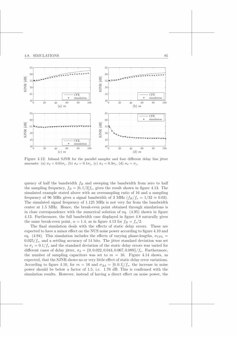
4.8. SIMULATIONS 85
(a) m
SJN
R[d
B]
(b) m
SJN
R[d
B]
(c) m
SJN
R[d
B]
SJN
R[d
B]
(d) m
CFEsimulation
CFEsimulation
CFEsimulation
CFEsimulation
0 20 40 60 80 1000 20 40 60 80 100
0 20 40 60 80 1000 20 40 60 80 100
40
45
50
55
60
65
40
45
50
55
60
65
40
45
50
55
60
65
40
45
50
55
60
65
Figure 4.12: Inband SJNR for the parallel sampler and four different delay line jitteramounts: (a) σd = 0.01σj , (b) σd = 0.1σj , (c) σd = 0.3σj , (d) σd = σj .
quency of half the bandwidth fB and sweeping the bandwidth from zero to halfthe sampling frequency, fB = [0, 1/2]fs, gives the result shown in figure 4.13. Thesimulated example stated above with an oversampling ratio of 16 and a samplingfrequency of 96 MHz gives a signal bandwidth of 3 MHz (fB/fs = 1/32 ≈ 0.03).The simulated signal frequency of 1.125 MHz is not very far from the bandwidthcenter at 1.5 MHz. Hence, the break-even point obtained through simulations isin close correspondence with the numerical solution of eq. (4.95) shown in figure4.13. Furthermore, the full bandwidth case displayed in figure 4.8 naturally givesthe same break-even point, α = 1.4, as in figure 4.13 for fB = fs/2.
The final simulation deals with the effects of static delay errors. These areexpected to have a minor effect on the NUS noise power according to figure 4.10 andeq. (4.94). This simulation includes the effects of varying phase-lengths, σVPL =0.025/fs, and a settling accuracy of 14 bits. The jitter standard deviation was setto σj = 0.1/fs and the standard deviation of the static delay errors was varied fordifferent cases of delay jitter, σd = {0, 0.022, 0.044, 0.067, 0.089}/fs. Furthermore,the number of sampling capacitors was set to m = 16. Figure 4.14 shows, asexpected, that the SJNR shows no or very little effect of static delay error variations.According to figure 4.10, for m = 16 and σΔd = [0, 0.1]/fs, the increase in noisepower should be below a factor of 1.5, i.e. 1.76 dB. This is confirmed with thesimulation results. However, instead of having a direct effect on noise power, the

86 CHAPTER 4. THE PARALLEL SAMPLER
α(σ
d=
ασ
j)
fB [fs]0 0.05 0.1 0.15 0.2 0.25 0.3 0.35 0.4 0.45 0.5
00.10.20.30.40.50.60.70.80.9
11.11.21.31.4
Figure 4.13: Break-even point, α, between clock jitter and delay jitter as function ofsignal bandwidth.
Closed-form Expression
σΔd [1/fs]
SJN
R[d
B]
Simulations
σΔd [1/fs]
SJN
R[d
B]
σd = 0σd = 0.022/fs
σd = 0.044/fs
σd = 0.067/fs
σd = 0.089/fs
σd = 0σd = 0.022/fs
σd = 0.044/fs
σd = 0.067/fs
σd = 0.089/fs
0 0.02 0.04 0.06 0.08 0.10 0.02 0.04 0.06 0.08 0.10
10
20
30
40
50
60
0
10
20
30
40
50
60
Figure 4.14: Full band SJNR as function of static delay errors for five different delayjitter magnitudes.

4.9. SUMMARY 87
static delay errors can have a substantial indirect effect by increasing the probabilityof overlap. In order to reduce the overlap probability, a trade-off has to be madebetween clock duty cycle (impacting phase overlap effects) and settling accuracy(impacting varying phase-length effects).
4.9 Summary
This chapter has presented the parallel sampler which obtains clock jitter tolerancethrough the process of averaging. Closed-form expressions of performance metricshave been presented that accurately predict the results obtained through simula-tions. Furthermore, nonidealities such as kBT/C noise and capacitor mismatcheffects have been investigated and it was shown that there is no significant degra-dation compared to an ordinary sampling circuit using one capacitor. Moreover,a method of generating the necessary clock signals from a single clock source waspresented in the form of a delay line. The properties of the delay line were analysedand degrading effects such as stochastic delay variations and static delay errorswere also treated.
Since the parallel sampler’s principle of operation is based on multiple clocksignals, synchronized but with statistically independent amounts of jitter on eachfalling edge, the clock generation circuit is the critical component of the parallelsampler. The clock generation circuit sets the maximum achievable non-uniformsampling noise suppression level together with the number of sampling capacitors.Static delay errors were shown to have a small direct impact on the NUS noisesuppressing properties of the parallel sampler whereas delay line jitter has a sig-nificant impact. Delay line jitter originates from intrinsic device noise as well aspower-supply noise and substrate noise. Hence, it is important to ensure that thedelay line is located in a low noise environment in order for the parallel sampler’snoise suppression capabilities to remain unhindered.

Chapter 5The Sigma-Delta Sampler
5.1 Introduction
This chapter will focus on presenting and analysing a sampling topology whichalleviates the timing uncertainty problems through noise shaping techniques. Theidea stems from the fact that eq. (4.1) is based on a bandwidth of fs/2 which meansthat if the spectral shape of the jitter-induced noise has an uneven distribution, abetter performance can be achieved if the signal band coincides with the frequencyband where the jitter impact is lower. The basis of this chapter is [4] in the list ofpublications.
5.2 Background
One way to reduce the impact of timing uncertainties in the sampling circuit is bymimicking the noise shaping approach used for quantization noise in Sigma-Deltamodulators. As described in section 2.5 on Sigma-Delta modulators, the idea is touse oversampling combined with a correlation circuit to achieve two objectives:
1. Spread the noise power over a larger frequency band (f ∈ [0, fs/2]) whichmeans the inband (fsig ∈ [0, fB ] or fsig ∈ [fBl, fBh]) noise power decreases ifproper filtering is done after sampling.
2. Spectrally shape the noise to have the center of mass outside the signal band.For low-pass ΣΔ modulators, this means having a noise transfer function ofa high-pass characteristic.
A straightforward approach is to look at continuous-time ΣΔ modulators whichhave the sampling circuit located in front of the quantizer and hence make thejitter-induced sampling noise experience the same NTF as the quantization noise.However, CT ΣΔ modulators suffer from the drawback that the jitter-induced noisein the feedback DAC is not noise shaped. If this drawback is further combined with
89

90 CHAPTER 5. THE SIGMA-DELTA SAMPLER
−
+
Vin(t)
IDAC(t)
time
IDAC(t)
to next ΣΔ stage
from feedback
R
C
Figure 5.1: Feedback model with DAC feedback current pulse of continuous-time ΣΔmodulator.
a coarse DAC for linearity reasons, the benefit of noise shaped jitter-induced noisediminishes. The benefit of noise shaping is more than compensated by the addednoise injected from the feedback loop. However, in 2001, steps were taken to al-leviate the jitter-injection problems in the feedback loop when Maurits Ortmannset. al. [71] presented a CT Sigma-Delta modulator with decreased jitter-sensitivitythrough modification of the DAC feedback pulse shape. Traditionally, the DACfeedback current pulse has a somewhat trapezoidal shape which means any timinguncertainty on either rising or falling edge will have a direct effect on the amountof charge fed back onto the continuous-time integrator (see fig. 5.1). An exam-ple of a single bit DAC simply consists of two wires, one connected to +Vref andthe other connected to −Vref and the V − I conversion is done with a resistor.Ortmanns proposed a simple technique to change the DAC feedback waveform byhaving the reference voltages charging and discharging a capacitor thus creating anexponentially decaying DAC current pulse (see fig. 5.2). From visual inspection itis clear that the charge variation of the exponentially shaped waveform is less thanthe trapezoidally shaped waveform if the starting and finishing time instants arevaried. To explain this in more detail, the charge variations for the two cases arecalculated and compared.
Q1 =∫ t�
t�IDAC,1(t)dt ≈ IDAC(t� − t�) = IDACTx + IDAC(γ� − γ�) (5.1)
where t� = γ�, t� = Tx + γ�, and Tx being a deterministic quantity describing howlong time the feedback operation takes. From the above relation it is evident thatthere are two jitter terms affecting the delivered charge. For the exponential case,the waveform is given by IDAC,2(t) = I2 exp((t − t�)/τ), where τ = RRCR is thetime constant of the feedback network. Furthermore, initial conditions state that
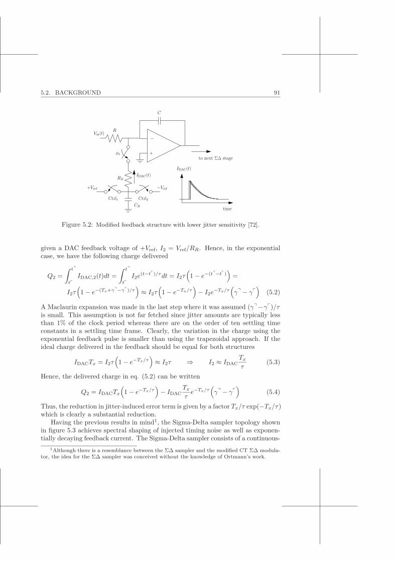
5.2. BACKGROUND 91
time
IDAC(t)
CR
−Vref+Vref
RR
−
+
Vin(t)
IDAC(t)
to next ΣΔ stage
R
C
φ1
Ctrl1 Ctrl2
Figure 5.2: Modified feedback structure with lower jitter sensitivity [72].
given a DAC feedback voltage of +Vref, I2 = Vref/RR. Hence, in the exponentialcase, we have the following charge delivered
Q2 =∫ t�
t�IDAC,2(t)dt =
∫ t�
t�I2e
(t−t�)/τdt = I2τ(1 − e−(t�−t�)
)=
I2τ(1 − e−(Tx+γ�−γ�)/τ
)≈ I2τ
(1 − e−Tx/τ
)− I2e
−Tx/τ(γ� − γ�
)(5.2)
A Maclaurin expansion was made in the last step where it was assumed (γ�−γ�)/τis small. This assumption is not far fetched since jitter amounts are typically lessthan 1% of the clock period whereas there are on the order of ten settling timeconstants in a settling time frame. Clearly, the variation in the charge using theexponential feedback pulse is smaller than using the trapezoidal approach. If theideal charge delivered in the feedback should be equal for both structures
IDACTx = I2τ(1 − e−Tx/τ
)≈ I2τ ⇒ I2 ≈ IDAC
Tx
τ(5.3)
Hence, the delivered charge in eq. (5.2) can be written
Q2 = IDACTx
(1 − e−Tx/τ
)− IDAC
Tx
τe−Tx/τ
(γ� − γ�
)(5.4)
Thus, the reduction in jitter-induced error term is given by a factor Tx/τ exp(−Tx/τ)which is clearly a substantial reduction.
Having the previous results in mind1, the Sigma-Delta sampler topology shownin figure 5.3 achieves spectral shaping of injected timing noise as well as exponen-tially decaying feedback current. The Sigma-Delta sampler consists of a continuous-
1Although there is a resemblance between the ΣΔ sampler and the modified CT ΣΔ modula-tor, the idea for the ΣΔ sampler was conceived without the knowledge of Ortmann’s work.
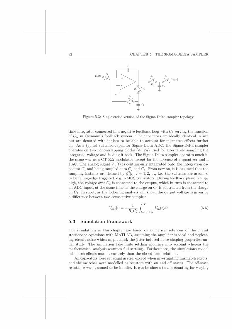
92 CHAPTER 5. THE SIGMA-DELTA SAMPLER
−
+
Vin(t)Vout[i]
C2
R3
φ2φ1
R2 φ1
R4
φ2
C1
C3
R1
Figure 5.3: Single-ended version of the Sigma-Delta sampler topology.
time integrator connected in a negative feedback loop with C2 serving the functionof CR in Ortmann’s feedback system. The capacitors are ideally identical in sizebut are denoted with indices to be able to account for mismatch effects furtheron. As a typical switched-capacitor Sigma-Delta ADC, the Sigma-Delta sampleroperates on two nonoverlapping clocks {φ1, φ2} used for alternately sampling theintegrated voltage and feeding it back. The Sigma-Delta sampler operates much inthe same way as a CT ΣΔ modulator except for the absence of a quantizer and aDAC. The analog signal Vin(t) is continuously integrated onto the integration ca-pacitor C1 and being sampled onto C2 and C3. From now on, it is assumed that thesampling instants are defined by φ�
1[i], i = 1, 2, . . ., i.e. the switches are assumedto be falling-edge triggered, e.g. NMOS transistors. During feedback phase, i.e. φ2
high, the voltage over C3 is connected to the output, which in turn is connected toan ADC input, at the same time as the charge on C2 is subtracted from the chargeon C1. In short, as the following analysis will show, the output voltage is given bya difference between two consecutive samples:
Vout[i] = − 1R1C2
∫ iT
t=(i−1)T
Vin(t)dt (5.5)
5.3 Simulation Framework
The simulations in this chapter are based on numerical solutions of the circuitstate-space equations with MATLAB, assuming the amplifier is ideal and neglect-ing circuit noise which might mask the jitter-induced noise shaping properties un-der study. The simulation take finite settling accuracy into account whereas themathematical analysis assumes full settling. Furthermore, the simulations modelmismatch effects more accurately than the closed-form relations.
All capacitors were set equal in size, except when investigating mismatch effects,and the switches were modelled as resistors with on and off states. The off-stateresistance was assumed to be infinite. It can be shown that accounting for varying
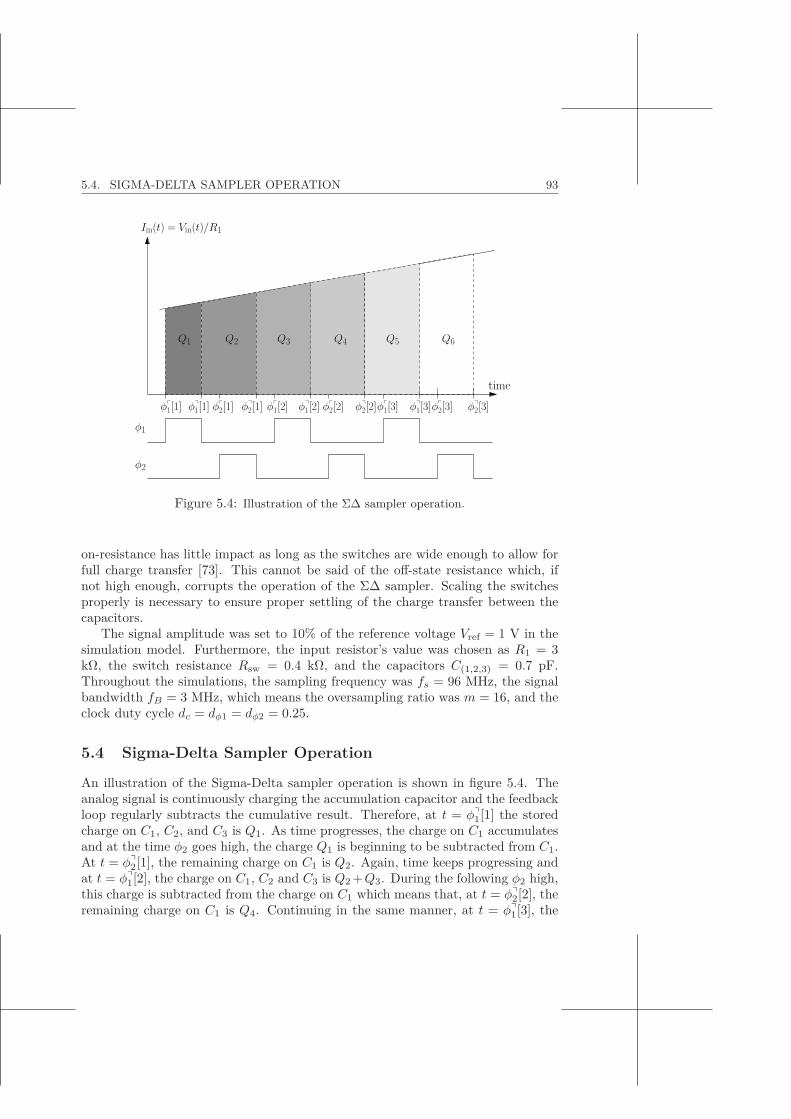
5.4. SIGMA-DELTA SAMPLER OPERATION 93
φ�2[3]φ�
2[3]φ�1[3]φ�
1[3]φ�2[2]φ�
2[2]φ�1[2]φ�
1[2]φ�2[1]φ�
2[1]φ�1[1]
Iin(t) = Vin(t)/R1
time
φ1
φ2
φ�1[1]
Q1 Q2 Q3 Q4 Q5 Q6
Figure 5.4: Illustration of the ΣΔ sampler operation.
on-resistance has little impact as long as the switches are wide enough to allow forfull charge transfer [73]. This cannot be said of the off-state resistance which, ifnot high enough, corrupts the operation of the ΣΔ sampler. Scaling the switchesproperly is necessary to ensure proper settling of the charge transfer between thecapacitors.
The signal amplitude was set to 10% of the reference voltage Vref = 1 V in thesimulation model. Furthermore, the input resistor’s value was chosen as R1 = 3kΩ, the switch resistance Rsw = 0.4 kΩ, and the capacitors C(1,2,3) = 0.7 pF.Throughout the simulations, the sampling frequency was fs = 96 MHz, the signalbandwidth fB = 3 MHz, which means the oversampling ratio was m = 16, and theclock duty cycle dc = dφ1 = dφ2 = 0.25.
5.4 Sigma-Delta Sampler Operation
An illustration of the Sigma-Delta sampler operation is shown in figure 5.4. Theanalog signal is continuously charging the accumulation capacitor and the feedbackloop regularly subtracts the cumulative result. Therefore, at t = φ�
1[1] the storedcharge on C1, C2, and C3 is Q1. As time progresses, the charge on C1 accumulatesand at the time φ2 goes high, the charge Q1 is beginning to be subtracted from C1.At t = φ�
2[1], the remaining charge on C1 is Q2. Again, time keeps progressing andat t = φ�
1[2], the charge on C1, C2 and C3 is Q2 +Q3. During the following φ2 high,this charge is subtracted from the charge on C1 which means that, at t = φ�
2[2], theremaining charge on C1 is Q4. Continuing in the same manner, at t = φ�
1[3], the

94 CHAPTER 5. THE SIGMA-DELTA SAMPLER
charge on C1, C2, and C3 is Q4 +Q5. A pattern emerges and it is clear that afterthe initial transient of sampling Q1 in the first clock cycle, the sampled charge isalways the integrated input current over a whole period of φ1, i.e.
Qsampled[i] =∫ φ�
1 [i]
φ�1 [i−1]
Iin(t)dt (5.6)
Having intuitively established how the Sigma-Delta sampler operates, a more de-tailed analysis follows.
The operation of the sampler is assumed to start from t = 0 in a situation whenall capacitors are discharged. Furthermore, it is considered that φ�
1[1] = 0 and thenonoverlapping clock notation from figure 3.4 is adopted. Moreover it is assumedthat the switch resistance is constant, R = R2 = R3 = R4, C = C1 = C2 = C3
and amplifier ideal. For a sinusoidal input signal Vin(t) = A sin(ωt), the followingdifferential equation for VC1(t) is obtained through KCL at the input port of theamplifier.
A sin(ωt)R1
= −C1VC1(t) (5.7)
Here the polarity of VC1(t) is defined as positive towards the output of the amplifier.Solving this equation through straightforward integration for t = φ�
1[1] → φ�1[1]
givesVC1(t) =
A
ωτ1
(cos
(ωt
)− cos(ωφ�
1[1]))
+ VC1
(φ�
1[1])︸ ︷︷ ︸
=0
(5.8)
where τ1 = R1C1 = R1C. KVL from the amplifier output to ground for VC2(t) andVC3(t) yield
−VC1(t) − τ2VC2(t) − VC2(t) = 0 (5.9)−VC1(t) − τ3VC3(t) − VC3(t) = 0 (5.10)
where τ2 = R2C2 = RC = τ , and τ3 = R3C3 = RC = τ . These equations arestructurally identical to eq. (3.4) which means their solutions are given by
VC2
(φ�
1[1]) ≈ A
ωτ1
(cos
(ω(φ�
1[1] − τ))− cos
(ωφ�
1[1]))
(5.11)
Vout[1] = VC3
(φ�
1[1]) ≈ A
ωτ1
(cos
(ω(φ�
1[1] − τ))− cos
(ωφ�
1[1]))
(5.12)
under the approximation of full settling and ω2τ2 1. In the time frame betweenφ�
1[1] and φ�2[1], the voltages over C2 and C3 don’t change unless there is leakage
from the capacitors. However, the voltage over C1 changes and continues followingeq. (5.8) until φ�
2[1]. At this point, the φ2 switches begin conducting which meansthe sampled voltage on C2 is subtracted from the accumulated charge on C1. More-over, the voltage over C3 either changes or not depending on what is connected to

5.4. SIGMA-DELTA SAMPLER OPERATION 95
the output node. The voltage over C1 at the end of the first feedback phase is givenby
VC1
(φ�
2[1]) ≈ A
ωτ1
(cos
(ωφ�
2[1])− cos
(ωφ�
1[1]))−
− C2
C1
A
ωτ1
(cos
(ω(φ�
1[1] − τ))− cos
(ωφ�
1[1]))
(5.13)
Simplifying this relation results in
VC1
(φ�
2[1]) ≈ A
ωτ1
[cos
(ωφ�
2[1])− cos
(ω(φ�
1[1] − τ))]
(5.14)
At the same time, C2 has discharged and, if full settling is assumed, is empty withzero voltage. Continuing to consider VC1(t), when both clocks are low, the relationin eq. (5.14) is the initial condition and eq. (5.8) can be used to obtain
VC1
(φ�
1[2]) ≈ A
ωτ1
(cos
(ωφ�
1[2])− cos
(ωφ�
2[1]))
+ VC1
(φ�
2[1])
(5.15)
Expanding the last term and consolidating (the terms dependent on φ�2[1] cancel
out) givesVC1
(φ�
1[2]) ≈ A
ωτ1
(cos
(ωφ�
1[2])− cos
(ω(φ�
1[1] − τ)))
(5.16)
It is clear that only the first term has changed between VC1
(φ�
2[1])
and VC1
(φ�
1[2]).
When the next sampling phase begins, i = 2, the approach in eq. (5.15) is usedbut with eq. (5.16) as initial value. Again, only the first term changes. Hence,
VC1
(φ�
1[2]) ≈ A
ωτ1
(cos
(ωφ�
1[2])− cos
(ω(φ�
1[1] − τ)))
(5.17)
As earlier, the sampled voltage over C2 is obtained by solving differential eq. (5.9)with VC1(t) given by eq. (5.17) for t = φ�
1[2] → φ�1[2].
VC2
(φ�
1[2]) ≈ A
ωτ1
(cos
(ω(φ�
1[2] − τ))− cos
(ω(φ�
1[1] − τ)))
(5.18)
The voltage over C3, i.e. Vout[2], is given by the same expression.
Vout[2] ≈ A
ωτ1
(cos
(ω(φ�
1[2] − τ))− cos
(ω(φ�
1[1] − τ)))
(5.19)
Proceeding in the same way, analysing the three capacitor voltages as time pro-gresses results in the following observation:
Vout[i] ≈ A
ωτ1
(cos
(ω(φ�
1[i] − τ))− cos
(ω(φ�
1[i− 1] − τ)))
(5.20)
96 CHAPTER 5. THE SIGMA-DELTA SAMPLER
This relation is valid for i = 2, 3, . . ., and is in accordance with eq. (5.5). Sinceφ�
1[i] = iT + γ�φ1[i], the output voltage, in the steady state i > 1, is given by
Vout[i] ≈ A
ωτ1
[cos
(ω(iT + γ�
φ1[i]− τ))− cos
(ω((i− 1)T + γ�
φ1[i− 1]− τ))] (5.21)
Making a Taylor expansion around t = iT − τ and t = (i− 1)T − τ , the error dueto non-uniform sampling is given by
VNUS[i] ≈ A
τ1
[γ�
φ1[i] sin(ω(iT − τ
))︸ ︷︷ ︸
s[i]
−γ�φ1[i− 1] sin
(ω((i− 1)T − τ
))︸ ︷︷ ︸
s[i−1]
](5.22)
To calculate the power spectrum SNUS(f), the autocorrelation function is formed,rNUS[i, p] = C{VNUS[i+p], VNUS[i]}. Recalling the relation in eq. (4.13) and realizingthat E{VNUS[i]} = 0, for all i, if zero mean jitter is assumed, leads to
rNUS[i, p] ≈ E
{(A
τ1
)2[γ�
φ1[i+ p]s[i+ p] − γ�φ1[i− 1 + p]s[i− 1 + p]
]·
·[γ�
φ1[i]s[i] − γ�φ1[i− 1]s[i− 1]
]}(5.23)
Expanding this relation gives
rNUS[i, p] ≈ A2
τ21
s[i+ p]s[i] E{γ�
φ1[i+ p]γ�φ1[i]
}︸ ︷︷ ︸
=σ2j , if p=0
−A2
τ21
s[i+ p]s[i− 1]·
· E{γ�
φ1[i+ p]γ�φ1[i− 1]
}︸ ︷︷ ︸
=σ2j , if p=−1
−A2
τ21
s[i− 1 + p]s[i] E{γ�
φ1[i− 1 + p]γ�φ1[i]
}︸ ︷︷ ︸
=σ2j , if p=1
+
+A2
τ21
s[i− 1 + p]s[i− 1] E{γ�
φ1[i− 1 + p]γ�φ1[i− 1]
}︸ ︷︷ ︸
=σ2j , if p=0
(5.24)
Hence it is possible to categorize the autocorrelation function according to the timeshift, p.
rNUS[i, p] ≈
⎧⎪⎪⎪⎪⎨⎪⎪⎪⎪⎩
(Aσj/τ1)2[sin2
(ω(iT − τ
))+ sin2
(ω((i− 1)T − τ
))], if p = 0
−(Aσj/τ1)2 sin2(ω(iT − τ
)), if p = 1
−(Aσj/τ1)2 sin2(ω((i− 1)T − τ
)), if p = −1
(5.25)
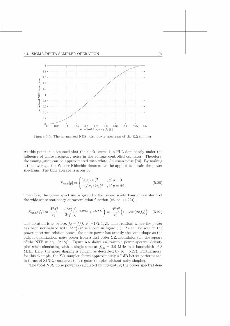
5.4. SIGMA-DELTA SAMPLER OPERATION 97
normalized frequency fd [fs]
norm
aliz
edN
US
noise
powe
r
0 0.05 0.1 0.15 0.2 0.25 0.3 0.35 0.4 0.45 0.50
0.2
0.4
0.6
0.8
1
1.2
1.4
1.6
1.8
2
Figure 5.5: The normalized NUS noise power spectrum of the ΣΔ sampler.
At this point it is assumed that the clock source is a PLL dominantly under theinfluence of white frequency noise in the voltage controlled oscillator. Therefore,the timing jitter can be approximated with white Gaussian noise [74]. By makinga time average, the Wiener-Khinchin theorem can be applied to obtain the powerspectrum. The time average is given by
rNUS[p] ≈{
(Aσj/τ1)2 , if p = 0−(Aσj/2τ1)2 , if p = ±1
(5.26)
Therefore, the power spectrum is given by the time-discrete Fourier transform ofthe wide-sense stationary autocorrelation function (cf. eq. (4.22)).
SNUS(fd) ≈A2σ2
j
τ21
− A2σ2j
2τ21
(e−j2πfd + ej2πfd
)=A2σ2
j
τ21
(1 − cos(2πfd)
)(5.27)
The notation is as before, fd = f/fs ∈ [−1/2, 1/2]. This relation, where the powerhas been normalized with A2σ2
j /τ21 is shown in figure 5.5. As can be seen in the
power spectrum relation above, the noise power has exactly the same shape as theoutput quantization noise power from a first order ΣΔ modulator (cf. the squareof the NTF in eq. (2.18)). Figure 5.6 shows an example power spectral densityplot when simulating with a single tone at fsig = 2.9 MHz in a bandwidth of 3MHz. Here, the noise shaping is evident as described by eq. (5.27). Furthermore,for this example, the ΣΔ sampler shows approximately 4.7 dB better performance,in terms of SJNR, compared to a regular sampler without noise shaping.
The total NUS noise power is calculated by integrating the power spectral den-

98 CHAPTER 5. THE SIGMA-DELTA SAMPLER
(a) frequency [MHz]
PSD
[dB
]
(b) frequency [MHz]
PSD
[dB
]inband SJNR = 84.6 dB
inband SJNR = 89.3 dB4.7 dB better SJNR
0 0.5 1 1.5 2 2.5 3
0 0.5 1 1.5 2 2.5 3
-150
-100
-50
0
-150
-100
-50
0
Figure 5.6: The NUS noise power spectral density of the ΣΔ sampler (b) compared withan ordinary sampler (a).
sity, SNUS(f)/fs, over the entire bandwidth.
PNUS ≈∫ 1/2
−1/2
A2σ2j
τ21
(1 − cos(2πfd)
)dfd =
A2σ2j
τ21
(5.28)
The total signal power is obtained from an average of the squared output signal,given by eq. (5.20), having no jitter.
Psig,out ≈ A2
ω2τ21
(cos
(ω(iT − τ)
)− cos(ω((i− 1)T − τ)
))2
(5.29)
Expanding the time average gives2
Psig,out ≈ A2
ω2τ21
limN→∞
1N
N+1∑i=2
cos2(ω(iT − τ)
)+ cos2
(ω((i− 1)T − τ)
)−− 2 cos
(ω(iT − τ)
)cos
(ω((i− 1)T − τ)
)(5.30)
2An alternative approach giving the same result is to use the relation cos(α) − cos(β) =−2 sin((α − β)/2) sin((α + β)/2).

5.4. SIGMA-DELTA SAMPLER OPERATION 99
Using fundamental trigonometric identities leads to
Psig,out ≈ A2
ω2τ21
(1 − cos(ωT ) − lim
N→∞1
2N
N+1∑i=2
cos(2ω(iT − τ)
)+
+ cos(2ω((i− 1)T − τ)
)+ 2 cos
(ω((2i− 1)T − 2τ)
))(5.31)
The limit can be calculated by using Euler’s formula. Instead of deducing the resultfor each of the terms, a general result will be shown that applies to all terms.
L = limN→∞
1N
N+k−1∑i=k
cos(ϕ1i+ ϕ2) = limN→∞
1N
N+k−1∑i=k
Re{ej(ϕ1i+ϕ2)
}(5.32)
Rewriting the above expression gives
L = limN→∞
1N
Re{N+k−1∑
i=k
ej(ϕ1i+ϕ2)
}= lim
N→∞1N
Re{ejϕ2
N+k−1∑i=k
ejϕ1i
}(5.33)
The geometric sum is found in a straightforward way as
N+k−1∑i=k
ejϕ1i =ejϕ1(N+k) − ejϕ1k
ejϕ1 − 1=
sin(ϕ1N/2)sin(ϕ1/2)
ejϕ1((N−1)/2+k) (5.34)
Hence, the limit becomes
L = limN→∞
1N
sin(ϕ1N/2)sin(ϕ1/2)
cos(ϕ1
((N − 1)/2 + k
)+ ϕ2
)= 0 (5.35)
for ϕ1 �= ±2nπ, n ∈ Z, since the sinus and cosine factors are constants. In the caseof ϕ1 = ±2nπ, the sum in eq. (5.32) trivially gives L = cos(ϕ2) but this case isvery unlikely to happen, requiring 2ωT = 2nπ, i.e.
2ωT = 2nπ ⇒ fsigfs
=n
2⇒ fsig
fs=
12
(5.36)
Hence, the average signal power at the ΣΔ sampler output is
Psig,out ≈ A2
ω2τ21
(1 − cos(ωT )
)=
2A2
τ21
(sin(ωT/2)
ω
)2
(5.37)
Making the approximation sin(x) ≈ x for small x gives
Psig,out ≈ 2A2
τ21
ωT
2ω=A2
2
(T
τ1
)2
(5.38)
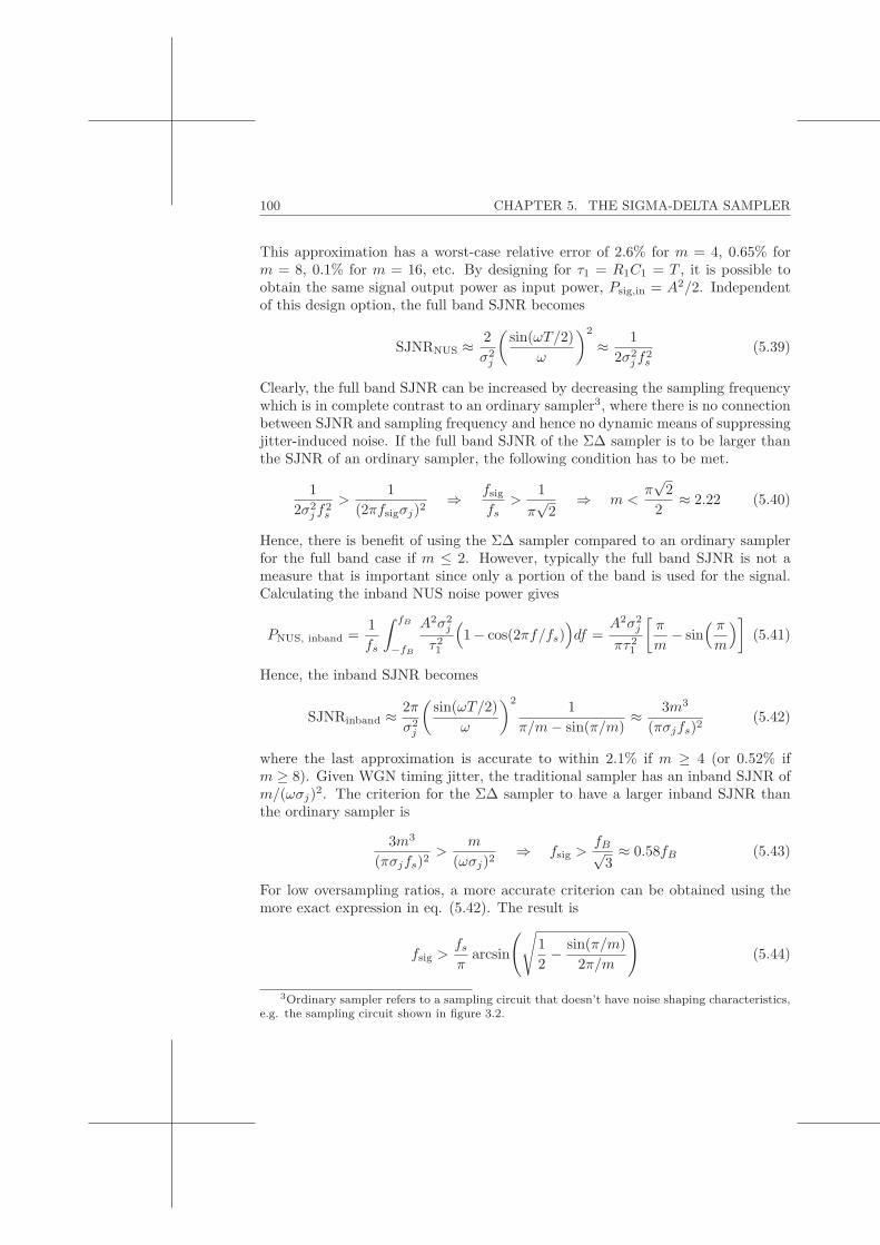
100 CHAPTER 5. THE SIGMA-DELTA SAMPLER
This approximation has a worst-case relative error of 2.6% for m = 4, 0.65% form = 8, 0.1% for m = 16, etc. By designing for τ1 = R1C1 = T , it is possible toobtain the same signal output power as input power, Psig,in = A2/2. Independentof this design option, the full band SJNR becomes
SJNRNUS ≈ 2σ2
j
(sin(ωT/2)
ω
)2
≈ 12σ2
j f2s
(5.39)
Clearly, the full band SJNR can be increased by decreasing the sampling frequencywhich is in complete contrast to an ordinary sampler3, where there is no connectionbetween SJNR and sampling frequency and hence no dynamic means of suppressingjitter-induced noise. If the full band SJNR of the ΣΔ sampler is to be larger thanthe SJNR of an ordinary sampler, the following condition has to be met.
12σ2
j f2s
>1
(2πfsigσj)2⇒ fsig
fs>
1π√
2⇒ m <
π√
22
≈ 2.22 (5.40)
Hence, there is benefit of using the ΣΔ sampler compared to an ordinary samplerfor the full band case if m ≤ 2. However, typically the full band SJNR is not ameasure that is important since only a portion of the band is used for the signal.Calculating the inband NUS noise power gives
PNUS, inband =1fs
∫ fB
−fB
A2σ2j
τ21
(1− cos(2πf/fs)
)df =
A2σ2j
πτ21
[π
m− sin
( πm
)](5.41)
Hence, the inband SJNR becomes
SJNRinband ≈ 2πσ2
j
(sin(ωT/2)
ω
)2 1π/m− sin(π/m)
≈ 3m3
(πσjfs)2(5.42)
where the last approximation is accurate to within 2.1% if m ≥ 4 (or 0.52% ifm ≥ 8). Given WGN timing jitter, the traditional sampler has an inband SJNR ofm/(ωσj)2. The criterion for the ΣΔ sampler to have a larger inband SJNR thanthe ordinary sampler is
3m3
(πσjfs)2>
m
(ωσj)2⇒ fsig >
fB√3≈ 0.58fB (5.43)
For low oversampling ratios, a more accurate criterion can be obtained using themore exact expression in eq. (5.42). The result is
fsig >fs
πarcsin
(√12− sin(π/m)
2π/m
)(5.44)
3Ordinary sampler refers to a sampling circuit that doesn’t have noise shaping characteristics,e.g. the sampling circuit shown in figure 3.2.
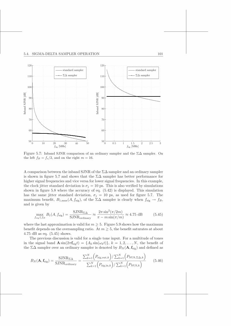
5.4. SIGMA-DELTA SAMPLER OPERATION 101
fsig [MHz]
Inba
ndSJ
NR
[dB]
fsig [MHz]
Inba
ndSJ
NR
[dB]
standard sampler
ΣΔ sampler
standard sampler
ΣΔ sampler
0 0.5 1 1.5 2 2.5 30 10 20 30 40 5050
60
70
80
90
100
110
120
50
60
70
80
90
100
110
120
Figure 5.7: Inband SJNR comparison of an ordinary sampler and the ΣΔ sampler. Onthe left fB = fs/2, and on the right m = 16.
A comparison between the inband SJNR of the ΣΔ sampler and an ordinary sampleris shown in figure 5.7 and shows that the ΣΔ sampler has better performance forhigher signal frequencies and vice versa for lower signal frequencies. In this example,the clock jitter standard deviation is σj = 10 ps. This is also verified by simulationsshown in figure 5.8 where the accuracy of eq. (5.42) is displayed. This simulationhas the same jitter standard deviation, σj = 10 ps, as used for figure 5.7. Themaximum benefit, B1,max(A, fsig), of the ΣΔ sampler is clearly when fsig → fB,and is given by
maxfsig≤fB
B1(A, fsig) =SJNRΣΔ
SJNRordinary≈ 2π sin2(π/2m)π −m sin(π/m)
≈ 4.75 dB (5.45)
where the last approximation is valid form ≥ 5. Figure 5.9 shows how the maximumbenefit depends on the oversampling ratio. At m ≥ 5, the benefit saturates at about4.75 dB as eq. (5.45) shows.
The previous discussion is valid for a single tone input. For a multitude of tonesin the signal band A sin(2πfsigt) = {Ak sin(ωkt)}, k = 1, 2, . . . , N , the benefit ofthe ΣΔ sampler over an ordinary sampler is denoted by BN (A, fsig) and defined as
BN (A, fsig) =SJNRΣΔ
SJNRordinary=
∑Nk=1
(Psig,out,k
)/∑N
k=1
(PNUS,ΣΔ,k
)∑N
k=1
(Psig,in,k
)/∑N
k=1
(PNUS,k
) (5.46)
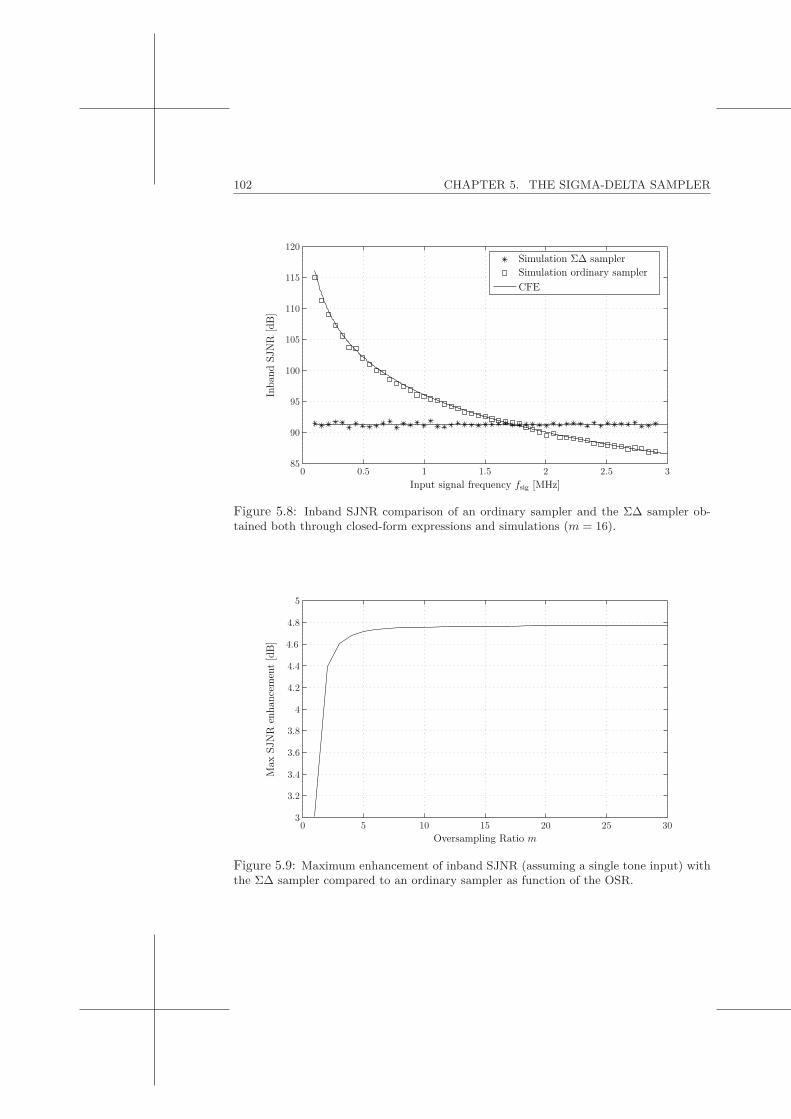
102 CHAPTER 5. THE SIGMA-DELTA SAMPLER
Input signal frequency fsig [MHz]
Inba
ndSJ
NR
[dB]
Simulation ΣΔ samplerSimulation ordinary samplerCFE
0 0.5 1 1.5 2 2.5 385
90
95
100
105
110
115
120
Figure 5.8: Inband SJNR comparison of an ordinary sampler and the ΣΔ sampler ob-tained both through closed-form expressions and simulations (m = 16).
Oversampling Ratio m
Max
SJN
Ren
hanc
emen
t[d
B]
0 5 10 15 20 25 303
3.2
3.4
3.6
3.8
4
4.2
4.4
4.6
4.8
5
Figure 5.9: Maximum enhancement of inband SJNR (assuming a single tone input) withthe ΣΔ sampler compared to an ordinary sampler as function of the OSR.

5.4. SIGMA-DELTA SAMPLER OPERATION 103
The terms in the previous expression are given by
Psig,out,k ≈ 2A2k
τ21
(sin(ωkT/2)
ωk
)2
Psig,in,k ≈ A2k
2(5.47)
PNUS,ΣΔ,k ≈ A2kσ
2j
πτ21
[π
m− sin
( πm
)]PNUS,k ≈ (Akωkσj)2
2m(5.48)
The total NUS noise for the ΣΔ sampling structure is
PNUS,ΣΔ ≈N∑
k=1
A2kσ
2j
πτ21
[π
m− sin
( πm
)]=
σ2j
πτ21
[π
m− sin
( πm
)] N∑k=1
A2k (5.49)
Similarly, the total NUS noise for the ordinary sampling structure is
PNUS ≈N∑
k=1
(Akωkσj)2
2m=
σ2j
2m
N∑k=1
(Akωk)2 (5.50)
The total signal power at the output of the ΣΔ sampler is
Psig,out ≈N∑
k=1
2A2k
τ21
(sin(ωkT/2)
ωk
)2
=T 2
2τ21
N∑k=1
A2k
(sin(ωkT/2)ωkT/2
)2
≈ T 2
2τ21
N∑k=1
A2k
(5.51)where the last approximation is valid for oversampling ratios, m ≥ 4. For theordinary sampler, the signal power is
Psig ≈ 12
N∑k=1
A2k (5.52)
Therefore, the SJNR for the ΣΔ sampler is
SJNRΣΔ ≈ (2/τ21 )
∑Nk=1A
2k sin2(ωkT/2)/ω2
k
(σ2j /πτ
21 )
(π/m− sin(π/m)
)∑Nk=1A
2k
≈ 3m3
(πσjfs)2(5.53)
where the last approximation is relatively accurate for m ≥ 4. This is the sameexpression as for a single tone in eq. (5.42) and just reflects the fact that, for nottoo low oversampling ratios, m ≥ 4, the NUS noise power of the ΣΔ sampler isindependent of the signal frequency. In contrast, the SJNR for the ordinary sampleris given by
SJNRordinary ≈ (1/2)∑N
k=1A2k
(σ2j /2m)
∑Nk=1A
2kω
2k
(5.54)
In the case of Ak = A for all k, i.e. the amplitudes of all tones are equal, theordinary sampler SJNR becomes
SJNRordinary|Ak=A ≈ NA2m
σ2jA
2∑N
k=1 ω2k
=m
σ2jω
2(5.55)

104 CHAPTER 5. THE SIGMA-DELTA SAMPLER
Clearly, the SJNR of the ordinary sampler depends strongly on where the masscenter of signal power is located in the spectrum. The benefit of the ΣΔ samplerover the standard sampler is
BN (A, fsig) ≈ 3fB
∑Nk=1A
2kf
2sig,k∑N
k=1A2k
(5.56)
As an example, for a continuous and uniform distribution of tones from f = 0 tof = fB and equal amplitudes for all tones, the benefit becomes
B∞(A, f) ≈ π3
6m3
1π/m− sin(π/m)
≈ 1 (5.57)
The approximation is accurate to approximately 13% for m = 2, 3% for m = 4,and becomes better as m grows. Hence, for an even frequency distribution, thereis no benefit of the ΣΔ sampler as compared to the ordinary sampler. However, ifmore signal power is higher in the band, the benefit is greater than 1 and is givenby
BN (A, fsig) ≈ 12m2
f2s
f2sig (5.58)
for m ≥ 4 and equal amplitudes for all tones. The maximum of eq. (5.58) coincideswith the single tone case of eq. (5.45).
Looking at another single tone case where the clock jitter standard deviation isvaried, the signal frequency is set to fsig = 2 MHz. Using the previously mentionedsampling frequency and bandwidth values gives a theoretical ΣΔ sampler benefitof
B1(A, fsig) ≈ 12m2
f2s
f2sig ≈ 1.33 ≈ 1.25 dB (5.59)
The predicted benefit shows good agreement with the simulation results displayedin figure 5.10.
5.5 Mismatch Effects
So far, the operation of the ΣΔ sampler has been described assuming perfectlymatched circuit elements. This section investigates the mismatch impact on thenoise shaping performance of the ΣΔ sampler.
The solution to differential equation (5.7) yields the solution in eq. (5.8), re-peated here for convenience.
VC1(t) =A
ωτ1
(cos
(ωt
)− cos(ωφ�
1[1]))
+ VC1
(φ�
1[1])︸ ︷︷ ︸
=0
(5.60)
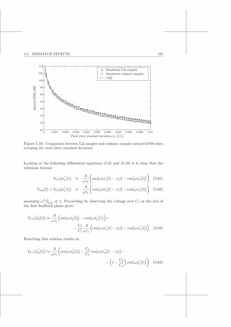
5.5. MISMATCH EFFECTS 105
Clock jitter standard deviation σj [1/fs]
Inba
ndSJ
NR
[dB]
Simulation ΣΔ samplerSimulation ordinary samplerCFE
0 0.001 0.002 0.003 0.004 0.005 0.006 0.007 0.008 0.009 0.0165
70
75
80
85
90
95
100
105
110
Figure 5.10: Comparison between ΣΔ sampler and ordinary sampler inband SJNR whensweeping the clock jitter standard deviation.
Looking at the following differential equations (5.9) and (5.10) it is clear that thesolutions become
VC2
(φ�
1[1]) ≈ A
ωτ1
(cos
(ω(φ�
1[1] − τ2))− cos
(ωφ�
1[1]))
(5.61)
Vout[1] = VC3
(φ�
1[1]) ≈ A
ωτ1
(cos
(ω(φ�
1[1] − τ3))− cos
(ωφ�
1[1]))
(5.62)
assuming ω2τ2(2,3) 1. Proceeding by observing the voltage over C1 at the end of
the first feedback phase gives
VC1
(φ�
2[1]) ≈ A
ωτ1
(cos
(ωφ�
2[1])− cos
(ωφ�
1[1]))−
− C2
C1
A
ωτ1
(cos
(ω(φ�
1[1] − τ2))− cos
(ωφ�
1[1]))
(5.63)
Rewriting this relation results in
VC1
(φ�
2[1]) ≈ A
ωτ1
(cos
(ωφ�
2[1])− C2
C1cos
(ω(φ�
1[1] − τ2))−
−(1 − C2
C1
)cos
(ωφ�
1[1]))
(5.64)

106 CHAPTER 5. THE SIGMA-DELTA SAMPLER
Proceeding to the next sampling instance at t = φ�1[2], the voltage over C1 has only
changed in the first term and is given by
VC1
(φ�
1[2]) ≈ A
ωτ1
(cos
(ωφ�
1[2])− C2
C1cos
(ω(φ�
1[1] − τ2))−
−(1 − C2
C1
)cos
(ωφ�
1[1]))
(5.65)
The voltage over C2 and C3 can, once again, be found by solving differential equa-tions (5.9) and (5.10) with VC1(t) given in eq. (5.65). The result is
VC2
(φ�
1[2]) ≈ A
ωτ1
(cos
(ω(φ�
1[2] − τ2))− C2
C1cos
(ω(φ�
1[1] − τ2))−
−(1 − C2
C1
)cos
(ωφ�
1[1]))
(5.66)
Vout[2] = VC3
(φ�
1[2]) ≈ A
ωτ1
(cos
(ω(φ�
1[2] − τ3))− C2
C1cos
(ω(φ�
1[1] − τ2))−
−(1 − C2
C1
)cos
(ωφ�
1[1]))
(5.67)
Continuing with the voltage over C1 at the end of the second feedback phase gives
VC1
(φ�
2[2]) ≈ A
ωτ1
(cos
(ωφ�
2[2])− C2
C1cos
(ω(φ�
1[2] − τ2))−
− C2
C1
(1 − C2
C1
)cos
(ω(φ�
1[1] − τ2)− (
1 − C2
C1
)2
cos(ωφ�
1[1]))
(5.68)
Hence, the three capacitor voltages, at the end of sampling phase three become
VC1
(φ�
1[3]) ≈ A
ωτ1
(cos
(ωφ�
1[3])− C2
C1cos
(ω(φ�
1[2] − τ2))−
− C2
C1
(1 − C2
C1
)cos
(ω(φ�
1[1] − τ2)− (
1 − C2
C1
)2
cos(ωφ�
1[1]))
(5.69)
VC2
(φ�
1[3]) ≈ A
ωτ1
(cos
(ω(φ�
1[3] − τ2))− C2
C1cos
(ω(φ�
1[2] − τ2))−
− C2
C1
(1 − C2
C1
)cos
(ω(φ�
1[1] − τ2)− (
1 − C2
C1
)2
cos(ωφ�
1[1]))
(5.70)

5.6. SUMMARY 107
Vout[3] = VC3
(φ�
1[3]) ≈ A
ωτ1
(cos
(ω(φ�
1[3] − τ3))− C2
C1cos
(ω(φ�
1[2] − τ2))−
− C2
C1
(1 − C2
C1
)cos
(ω(φ�
1[1] − τ2)− (
1 − C2
C1
)2
cos(ωφ�
1[1]))
(5.71)
Denoting the capacitor mismatch as in section 4.3.2, C2 = C1(1+ εC) and the timeconstant mismatch τ2 = τ3(1 + ετ ) gives the following output voltage
Vout[3] ≈ A
ωτ1
(cos
(ω(φ�
1[3] − τ3))− (1 + εC) cos
(ω(φ�
1[2] − τ3(1 + ετ )))+
+ εC(1 + εC) cos(ω(φ�
1[1] − τ2)− ε2C cos
(ωφ�
1[1]))
(5.72)
Since εC ∼ 0.001, [42], the last term is neglected. Furthermore, since ετ ∼ 0.2,[42], and the fact that ωτ(2,3) 1, the phase deviation due to the time constant isneglected and the notation τ = τ2 = τ3 is used for simplicity. Hence, the outputvoltage can be approximated
Vout[3] ≈ A
ωτ1
(cos
(ω(φ�
1[3] − τ))− (1 + εC) cos
(ω(φ�
1[2] − τ))+
+ εC cos(ω(φ�
1[1] − τ))
(5.73)
By denoting Vout[i] = V idealout [i] + V mismatch
out [i] it is possible to isolate the mismatchterms.
V mismatchout [i] ≈ −AεC
ωτ1
(cos
(ω(φ�
1[i− 1] − τ))− cos
(ω(φ�
1[i− 2] − τ))
(5.74)
Since the mismatch terms are clearly much smaller than the ideal terms it is con-cluded that the effects on the NUS noise power will be very small. Furthermore,because the feedback errors due to mismatch decrease geometrically as the timedistance between present and past samples increases, there is no amplification overtime of the nonidealities. This is also shown in the following simulation resultswhere there is no discernible effect on the SJNR as the capacitor mismatch stan-dard deviation is swept from zero to 5% (see fig. 5.11). Also, there is no impactin the frequency spectrum from mismatch showing that the ΣΔ sampler is robustagainst capacitor mismatches. The signal frequency was set to fsig = 2 MHz andthe jitter standard deviation was σj = 10 ps.
5.6 Summary
This chapter has presented the Sigma-Delta sampler and made a performance com-parison with an ordinary sampler. It has been shown that the ΣΔ sampler has
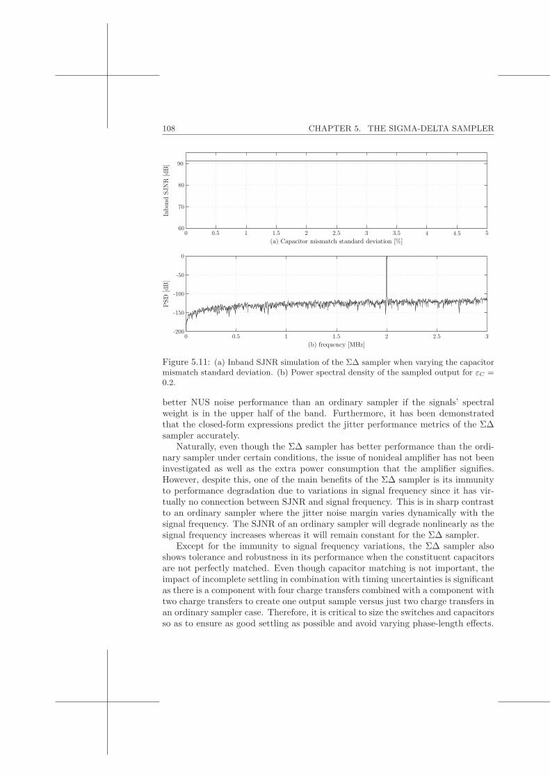
108 CHAPTER 5. THE SIGMA-DELTA SAMPLER
(a) Capacitor mismatch standard deviation [%]
Inba
ndSJ
NR
[dB]
PSD
[dB]
(b) frequency [MHz]0 0.5 1 1.5 2 2.5 3
0 0.5 1 1.5 2 2.5 3 3.5 4 4.5 5
-200
-150
-100
-50
0
60
70
80
90
Figure 5.11: (a) Inband SJNR simulation of the ΣΔ sampler when varying the capacitormismatch standard deviation. (b) Power spectral density of the sampled output for εC =0.2.
better NUS noise performance than an ordinary sampler if the signals’ spectralweight is in the upper half of the band. Furthermore, it has been demonstratedthat the closed-form expressions predict the jitter performance metrics of the ΣΔsampler accurately.
Naturally, even though the ΣΔ sampler has better performance than the ordi-nary sampler under certain conditions, the issue of nonideal amplifier has not beeninvestigated as well as the extra power consumption that the amplifier signifies.However, despite this, one of the main benefits of the ΣΔ sampler is its immunityto performance degradation due to variations in signal frequency since it has vir-tually no connection between SJNR and signal frequency. This is in sharp contrastto an ordinary sampler where the jitter noise margin varies dynamically with thesignal frequency. The SJNR of an ordinary sampler will degrade nonlinearly as thesignal frequency increases whereas it will remain constant for the ΣΔ sampler.
Except for the immunity to signal frequency variations, the ΣΔ sampler alsoshows tolerance and robustness in its performance when the constituent capacitorsare not perfectly matched. Even though capacitor matching is not important, theimpact of incomplete settling in combination with timing uncertainties is significantas there is a component with four charge transfers combined with a component withtwo charge transfers to create one output sample versus just two charge transfers inan ordinary sampler case. Therefore, it is critical to size the switches and capacitorsso as to ensure as good settling as possible and avoid varying phase-length effects.

Chapter 6Jitter Generation in Nonoverlapping ClockGeneration Circuits
6.1 Introduction
As process technology moves deeper into the nanometer domain and transistorspeeds improve, ADC architectures traditionally used for low frequency applica-tions, such as the Sigma-Delta modulator, become viable choices for use at higherfrequencies. The benefit of the Sigma-Delta modulator is, as described in chap-ter 2, that it takes advantage of digital signal processing, which makes it a goodcandidate for analog and mixed signal applications in deep submicron technologies.Unfortunately, this means that the ADC becomes more vulnerable to power-supplynoise (PSN) and substrate noise due to the limited isolation possibilities that comealong with sharing the same die as noisy digital blocks. Naturally, analog circuitsare very sensitive to power-supply noise since they are dependent on stable biaspoints. A shift in the supply or ground will alter the operation or bias points andwill affect vital performance metrics, such as linearity and gain, of the circuit. Fordigital logic, the situation is not as severe since noise margins are usually wideenough to swallow PSN without triggering a false transition. However, the timingproperties of a digital block will be affected by any change in the supply or ground.Thus, any PSN affecting a clock generation circuit (CGC) used for ADCs will intro-duce timing jitter on the sampling instants and possibly in other locations where atransition is made between analog and time-discrete domain, e.g. in the feedbackpath in continuous-time Sigma-Delta ADCs. Therefore, an understanding of howPSN translates into timing jitter is imperative for digital circuits that are usedto alter the timing reference of a mixed signal system. In this dissertation, bothPSN and substrate noise are referred to by the term power-supply noise becausethe transistors’ bulk contacts are connected to either power or ground which meansthat voltage variations in the substrate translate to a variation in power-supply andvice versa.
109
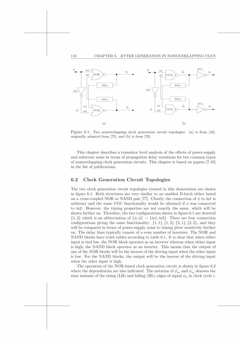
110 CHAPTER 6. JITTER GENERATION IN NONOVERLAPPING CGCS
(b)(a)
φ2
φ1
φ2
φ1
delay1
delay2
in2in1
φ
in2in1φ
φ2
φ1in1
in2
delay1
delay2
in1
in2φ
INV
φ
NAND2
NAND1
INV1
INV2
INV
NOR1
NOR2
Figure 6.1: Two nonoverlapping clock generation circuit topologies. (a) is from [42],originally adopted from [75], and (b) is from [76].
This chapter describes a transistor level analysis of the effects of power-supplyand substrate noise in terms of propagation delay variations for two common typesof nonoverlapping clock generation circuits. This chapter is based on papers [7-10]in the list of publications.
6.2 Clock Generation Circuit Topologies
The two clock generation circuit topologies treated in this dissertation are shownin figure 6.1. Both structures are very similar to an enabled D-latch either basedon a cross-coupled NOR or NAND pair [77]. Clearly, the connection of φ to in1 isarbitrary and the same CGC functionality would be obtained if φ was connectedto in2. However, the timing properties are not exactly the same, which will beshown further on. Therefore, the two configurations shown in figure 6.1 are denoted{1, 2} which is an abbreviation of {φ, φ} → {in1, in2}. There are four connectionconfigurations giving the same functionality: {1, 1}, {1, 2}, {2, 1}, {2, 2}, and theywill be compared in terms of power-supply noise to timing jitter sensitivity furtheron. The delay lines typically consist of a even number of inverters. The NOR andNAND blocks have truth tables according to table 6.1. It is clear that when eitherinput is tied low, the NOR block operates as an inverter whereas when either inputis high, the NAND block operates as an inverter. This means that the output ofone of the NOR blocks will be the inverse of the driving input when the other inputis low. For the NAND blocks, the output will be the inverse of the driving inputwhen the other input is high.
The operation of the NOR-based clock generation circuit is shown in figure 6.2where the dependencies are also indicated. The notation of φ�
xi and φ�xi denotes the
time instants of the rising (LH) and falling (HL) edges of signal φx in clock cycle i.

6.2. CLOCK GENERATION CIRCUIT TOPOLOGIES 111
Table 6.1: NAND and NOR truth tablein1 in2 NOR NAND0 0 1 10 1 0 11 0 0 11 1 0 0
nonoverlap timenonoverlap time
LH
HL
LH
HL
LH
HLLH φ�2 φ�
2
period 1 period 2 period 3
φ
delay2
delay1
φ
φ
φ1
φ2
φ1
φ2φ
time
Figure 6.2: Transition paths and approximate timing diagram of the NOR-based clockgeneration circuit.
The rising edge of φ triggers a falling edge on φ1 and a rising edge of φ, i.e. a fallingedge of φ triggers a falling edge on φ2. The falling edge on φ1 in turn triggers arising edge on φ2 and a falling edge of φ2 triggers a rising edge on φ1. So the fallingedges of {φ1, φ2} are controlled by φ whereas each rising edge is controlled by theother clock’s falling edge. These timing dependencies can be written
φ�1i = φ�
i + dNOR1(φ�i ) (6.1)
φ�1i = φ�
2i + dd2(φ�2i) + dNOR1(φ
�2i + dd2(φ�
2i)) (6.2)
φ�2i = φ�
1i + dd1(φ�1i) + dNOR2(φ
�1i + dd1(φ�
1i)) (6.3)
φ�2i = φ�
i + dNOR2(φ�i ) (6.4)
where φ�i = φ�
i + dINV(φ�i ) which also is valid for the opposite transition direction.
The notation dx refers to the propagation delay of block x and d1 and d2 areabbreviations for delay line 1 and delay line 2. The purpose of the delay linesis apparent from eqs. (6.2) and (6.3): to increase the nonoverlap time betweenφ1 and φ2. However, as is evident from the same equations, the clocks will benonoverlapping even without the delay lines, since dNOR(1,2) are always positive.Therefore, the delay lines have not been included in the simulations.
Similarly, the NAND-based CGC operates according to figure 6.3. In this case,the falling edges of {φ1, φ2} are also controlled by φ whereas each corresponding
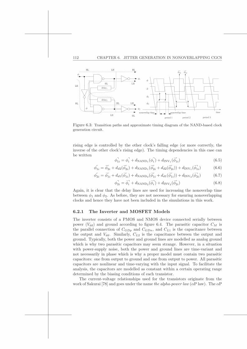
112 CHAPTER 6. JITTER GENERATION IN NONOVERLAPPING CGCS
φ�12φ�
12
period 3period 2
HLHL LH
HL LH
LH
HL
LH HL
HL LH
period 1
nonoverlap time nonoverlap timeφ2
φ1
φ
time
φ2
φ1
φ
φ
delay1
delay2
φ
Figure 6.3: Transition paths and approximate timing diagram of the NAND-based clockgeneration circuit.
rising edge is controlled by the other clock’s falling edge (or more correctly, theinverse of the other clock’s rising edge). The timing dependencies in this case canbe written
φ�1i = φ�
i + dNAND1(φ�i ) + dINV1(φ
�1i) (6.5)
φ�1i = φ�
2i + dd2(φ�2i) + dNAND1(φ
�2i + dd2(φ�
2i)) + dINV1(φ�1i) (6.6)
φ�2i = φ�
1i + dd1(φ�1i) + dNAND2(φ
�1i + dd1(φ�
1i)) + dINV2(φ�2i) (6.7)
φ�2i = φ�
i + dNAND2(φ�i ) + dINV2(φ
�2i) (6.8)
Again, it is clear that the delay lines are used for increasing the nonoverlap timebetween φ1 and φ2. As before, they are not necessary for ensuring nonoverlappingclocks and hence they have not been included in the simulations in this work.
6.2.1 The Inverter and MOSFET ModelsThe inverter consists of a PMOS and NMOS device connected serially betweenpower (Vdd) and ground according to figure 6.4. The parasitic capacitor CM isthe parallel connection of CGDp and CGDn, and CL1 is the capacitance betweenthe output and Vdd. Similarly, CL2 is the capacitance between the output andground. Typically, both the power and ground lines are modelled as analog groundwhich is why two parasitic capacitors may seem strange. However, in a situationwith power-supply noise, both the power and ground lines are time-variant andnot necessarily in phase which is why a proper model must contain two parasiticcapacitors: one from output to ground and one from output to power. All parasiticcapacitors are nonlinear and time-varying with the input signal. To facilitate theanalysis, the capacitors are modelled as constant within a certain operating rangedetermined by the biasing conditions of each transistor.
The current-voltage relationships used for the transistors originate from thework of Sakurai [78] and goes under the name the alpha-power law (αP law). The αP
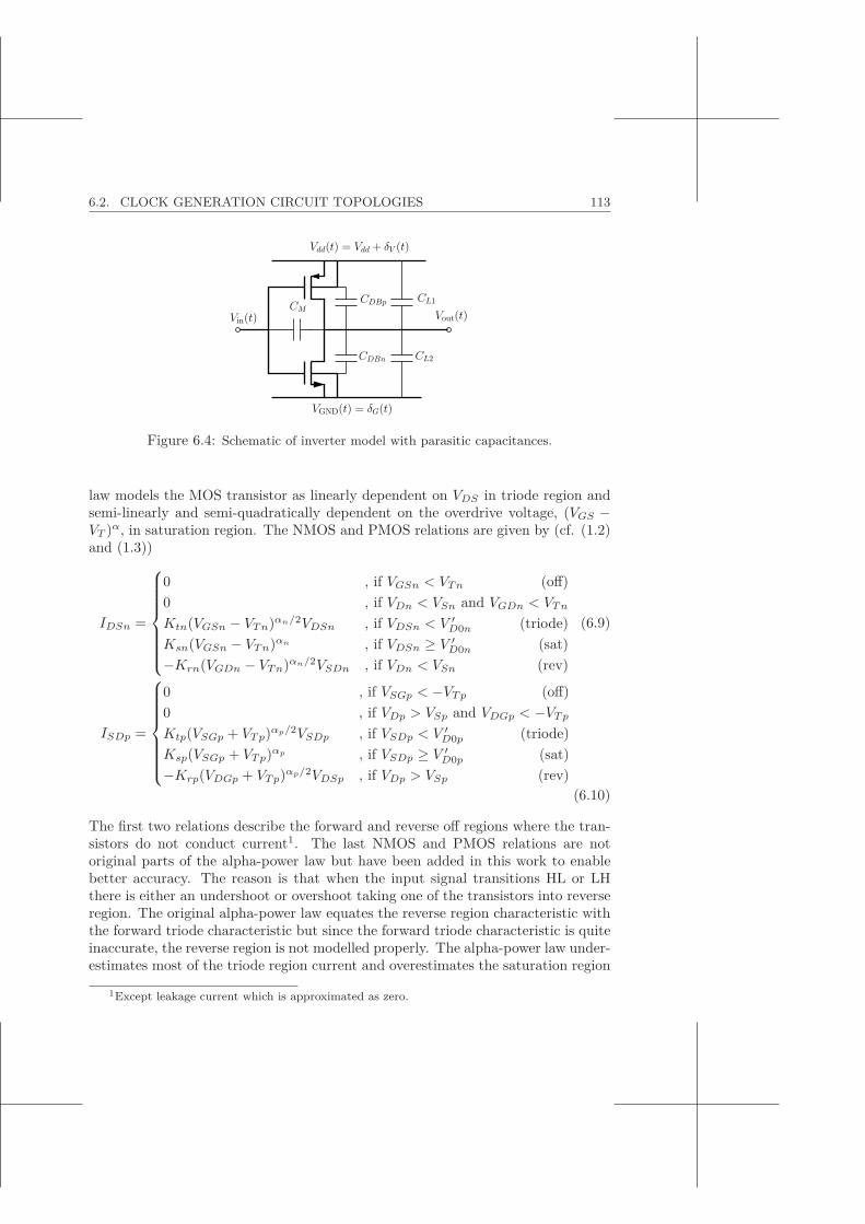
6.2. CLOCK GENERATION CIRCUIT TOPOLOGIES 113
CL2
CL1
Vout(t)
CDBp
CDBn
VGND(t) = δG(t)
Vdd(t) = Vdd + δV (t)
CMVin(t)
Figure 6.4: Schematic of inverter model with parasitic capacitances.
law models the MOS transistor as linearly dependent on VDS in triode region andsemi-linearly and semi-quadratically dependent on the overdrive voltage, (VGS −VT )α, in saturation region. The NMOS and PMOS relations are given by (cf. (1.2)and (1.3))
IDSn =
⎧⎪⎪⎪⎪⎪⎪⎨⎪⎪⎪⎪⎪⎪⎩
0 , if VGSn < VTn (off)0 , if VDn < VSn and VGDn < VTn
Ktn(VGSn − VTn)αn/2VDSn , if VDSn < V ′D0n (triode)
Ksn(VGSn − VTn)αn , if VDSn ≥ V ′D0n (sat)
−Krn(VGDn − VTn)αn/2VSDn , if VDn < VSn (rev)
(6.9)
ISDp =
⎧⎪⎪⎪⎪⎪⎪⎨⎪⎪⎪⎪⎪⎪⎩
0 , if VSGp < −VTp (off)0 , if VDp > VSp and VDGp < −VTp
Ktp(VSGp + VTp)αp/2VSDp , if VSDp < V ′D0p (triode)
Ksp(VSGp + VTp)αp , if VSDp ≥ V ′D0p (sat)
−Krp(VDGp + VTp)αp/2VDSp , if VDp > VSp (rev)(6.10)
The first two relations describe the forward and reverse off regions where the tran-sistors do not conduct current1. The last NMOS and PMOS relations are notoriginal parts of the alpha-power law but have been added in this work to enablebetter accuracy. The reason is that when the input signal transitions HL or LHthere is either an undershoot or overshoot taking one of the transistors into reverseregion. The original alpha-power law equates the reverse region characteristic withthe forward triode characteristic but since the forward triode characteristic is quiteinaccurate, the reverse region is not modelled properly. The alpha-power law under-estimates most of the triode region current and overestimates the saturation region
1Except leakage current which is approximated as zero.
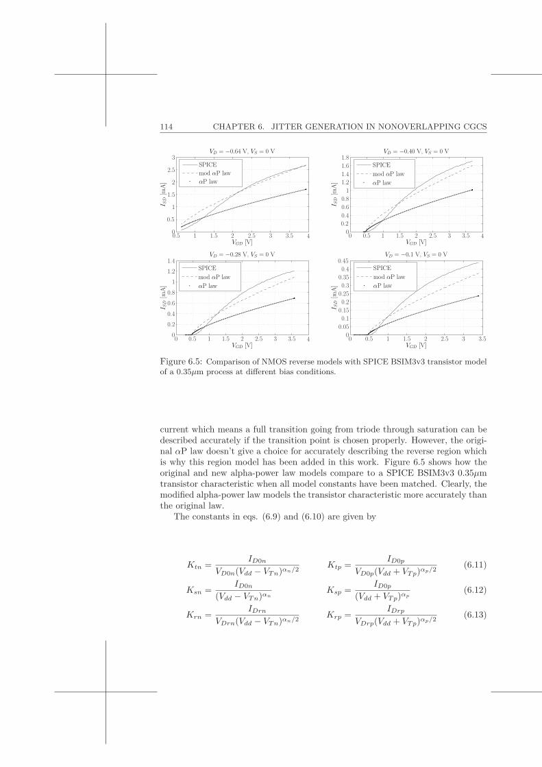
114 CHAPTER 6. JITTER GENERATION IN NONOVERLAPPING CGCS
VGD [V]
I SD
[mA
]
VD = −0.64 V, VS = 0 V
VGD [V]
I SD
[mA
]
VD = −0.40 V, VS = 0 V
VGD [V]
I SD
[mA
]
VD = −0.28 V, VS = 0 V
VGD [V]
I SD
[mA
]
VD = −0.1 V, VS = 0 V
SPICEmod αP lawαP law
SPICEmod αP lawαP law
SPICEmod αP lawαP law
SPICEmod αP lawαP law
0 0.5 1 1.5 2 2.5 3 3.50 0.5 1 1.5 2 2.5 3 3.5 4
0 0.5 1 1.5 2 2.5 3 3.5 40.5 1 1.5 2 2.5 3 3.5 4
00.050.1
0.150.2
0.250.3
0.350.4
0.45
00.20.40.60.8
11.21.4
00.20.40.60.8
11.21.41.61.8
0
0.5
1
1.5
2
2.5
3
Figure 6.5: Comparison of NMOS reverse models with SPICE BSIM3v3 transistor modelof a 0.35μm process at different bias conditions.
current which means a full transition going from triode through saturation can bedescribed accurately if the transition point is chosen properly. However, the origi-nal αP law doesn’t give a choice for accurately describing the reverse region whichis why this region model has been added in this work. Figure 6.5 shows how theoriginal and new alpha-power law models compare to a SPICE BSIM3v3 0.35μmtransistor characteristic when all model constants have been matched. Clearly, themodified alpha-power law models the transistor characteristic more accurately thanthe original law.
The constants in eqs. (6.9) and (6.10) are given by
Ktn =ID0n
VD0n(Vdd − VTn)αn/2Ktp =
ID0p
VD0p(Vdd + VTp)αp/2(6.11)
Ksn =ID0n
(Vdd − VTn)αnKsp =
ID0p
(Vdd + VTp)αp(6.12)
Krn =IDrn
VDrn(Vdd − VTn)αn/2Krp =
IDrp
VDrp(Vdd + VTp)αp/2(6.13)
6.3. ANALYSIS AND SIMULATION FRAMEWORK 115
where
ID0n = IDSn at VGSn = VDSn = Vdd (6.14)ID0p = ISDp at VSGp = VSDp = Vdd (6.15)IDrn = ISDn at VSGn = Vdd and VSDn = VDrn (6.16)IDrp = IDSp at VDGp = Vdd and VDSp = VDrp (6.17)VD0n = VDSn,sat at VGSn = Vdd (6.18)VD0p = VSDp,sat at VSGp = Vdd (6.19)
Here the reverse region MOSFET still uses the same node name as the forwardregion MOSFET, i.e. the node name is independent of node voltage conditions.The voltage constants V ′
D0n and V ′D0p in eqs. (6.9) and (6.10) are defined as
V ′D0n = VD0n
(VGSn − VTn
Vdd − VTn
)αn/2
(6.20)
V ′D0p = VD0p
(VSGp + VTp
Vdd + VTp
)αp/2
(6.21)
Example characteristics showing how the forward NMOS alpha-power law modelcompares with SPICE BSIM3v3 transistor models are shown in figure 6.6. In theIDSn vs. VGSn plot, the exponent α has been chosen such that the two curvesmatch. In the IDSn vs. VDSn plot, VD0n has been chosen so that the averageSPICE and αP law drain-source currents are equal as VDSn : 0 → Vdd.
6.2.2 The NAND and NOR BlocksThe NAND and NOR block schematics including the parasitic capacitors are shownin figure 6.7. The NMOS transistors in the NAND gate were scaled to twice theinverter NMOS size to compensate for the serial connection. However, the PMOStransistors in the NOR gate were not scaled larger since they are already approx-imately three times larger than their NMOS counterparts. The NAND and NORblocks are also assumed to be connected to another logic block which is why thereare two parasitic output capacitors, CL1 and CL2. The bulk contacts for transis-tors p2 and n1 were connected to the supply for area efficiency even though for theanalysis purposes, either configuration would be acceptable.
It is clear from the schematics that the NAND and NOR functionality is thatof an inverter if one of the inputs is kept high and low respectively.
6.3 Analysis and Simulation Framework
The Spectre simulation tool from Cadence with transistor models at BSIM3v3level2 was used for simulating the logic blocks and clock generation circuits. MAT-
2This simulation level is onwards referred to as SPICE simulation.
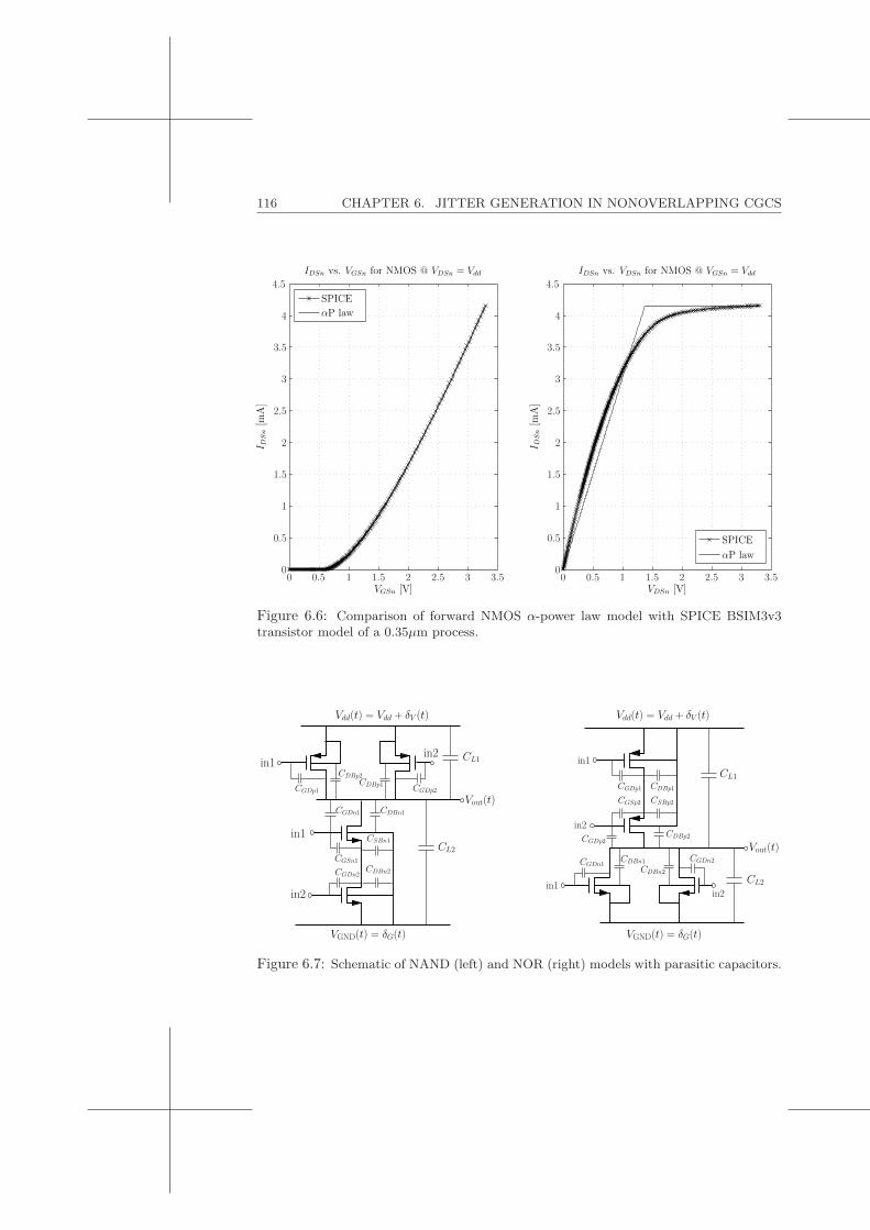
116 CHAPTER 6. JITTER GENERATION IN NONOVERLAPPING CGCS
VGSn [V]
I DS
n[m
A]
IDSn vs. VGSn for NMOS @ VDSn = Vdd
SPICEαP law
VDSn [V]
I DS
n[m
A]
IDSn vs. VDSn for NMOS @ VGSn = Vdd
SPICEαP law
0 0.5 1 1.5 2 2.5 3 3.50 0.5 1 1.5 2 2.5 3 3.50
0.5
1
1.5
2
2.5
3
3.5
4
4.5
0
0.5
1
1.5
2
2.5
3
3.5
4
4.5
Figure 6.6: Comparison of forward NMOS α-power law model with SPICE BSIM3v3transistor model of a 0.35μm process.
VGND(t) = δG(t)
Vdd(t) = Vdd + δV (t)
VGND(t) = δG(t)
Vdd(t) = Vdd + δV (t)
CGDp2CGDp1
CGDn1
CGSn1
CGDn2
in2in1
in2
in1in1in2
in2
in1
CDBp1
Vout(t)CDBn1
CDBn2
CGDp2
CSBp2CGSp2
CGDp1
CL1
CL2
CGDn2CGDn1
CDBp2
Vout(t)
CL2
CL1
CDBp2CDBp1
CDBn1
CDBn2
CSBn1
Figure 6.7: Schematic of NAND (left) and NOR (right) models with parasitic capacitors.
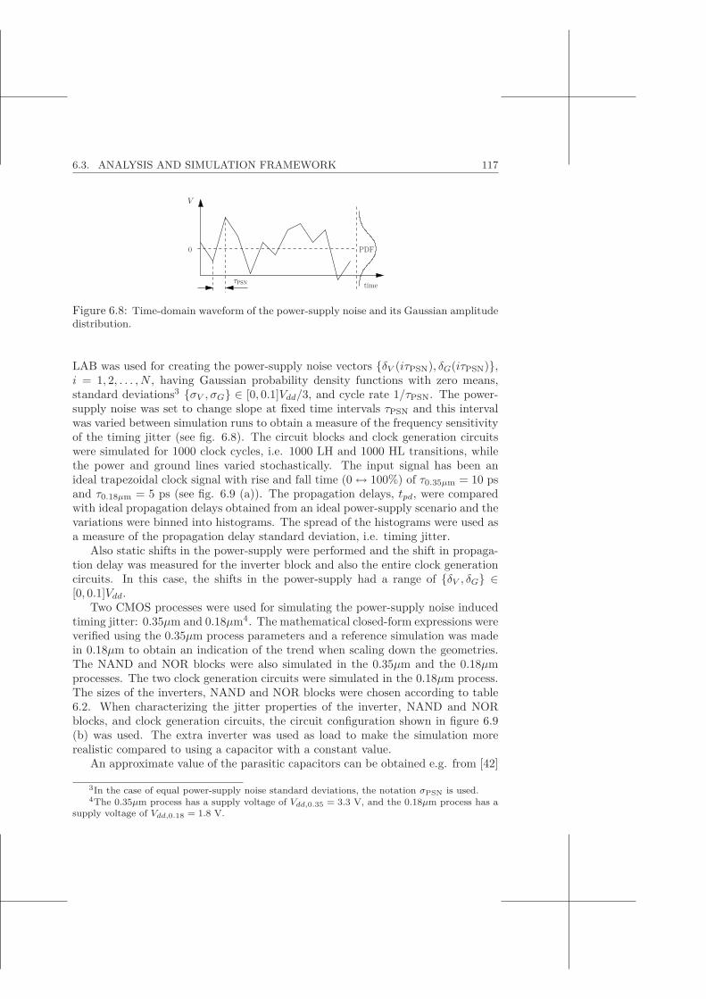
6.3. ANALYSIS AND SIMULATION FRAMEWORK 117
τPSN
0
V
time
Figure 6.8: Time-domain waveform of the power-supply noise and its Gaussian amplitudedistribution.
LAB was used for creating the power-supply noise vectors {δV (iτPSN), δG(iτPSN)},i = 1, 2, . . . , N , having Gaussian probability density functions with zero means,standard deviations3 {σV , σG} ∈ [0, 0.1]Vdd/3, and cycle rate 1/τPSN. The power-supply noise was set to change slope at fixed time intervals τPSN and this intervalwas varied between simulation runs to obtain a measure of the frequency sensitivityof the timing jitter (see fig. 6.8). The circuit blocks and clock generation circuitswere simulated for 1000 clock cycles, i.e. 1000 LH and 1000 HL transitions, whilethe power and ground lines varied stochastically. The input signal has been anideal trapezoidal clock signal with rise and fall time (0 ↔ 100%) of τ0.35μm = 10 psand τ0.18μm = 5 ps (see fig. 6.9 (a)). The propagation delays, tpd, were comparedwith ideal propagation delays obtained from an ideal power-supply scenario and thevariations were binned into histograms. The spread of the histograms were used asa measure of the propagation delay standard deviation, i.e. timing jitter.
Also static shifts in the power-supply were performed and the shift in propaga-tion delay was measured for the inverter block and also the entire clock generationcircuits. In this case, the shifts in the power-supply had a range of {δV , δG} ∈[0, 0.1]Vdd.
Two CMOS processes were used for simulating the power-supply noise inducedtiming jitter: 0.35μm and 0.18μm4. The mathematical closed-form expressions wereverified using the 0.35μm process parameters and a reference simulation was madein 0.18μm to obtain an indication of the trend when scaling down the geometries.The NAND and NOR blocks were also simulated in the 0.35μm and the 0.18μmprocesses. The two clock generation circuits were simulated in the 0.18μm process.The sizes of the inverters, NAND and NOR blocks were chosen according to table6.2. When characterizing the jitter properties of the inverter, NAND and NORblocks, and clock generation circuits, the circuit configuration shown in figure 6.9(b) was used. The extra inverter was used as load to make the simulation morerealistic compared to using a capacitor with a constant value.
An approximate value of the parasitic capacitors can be obtained e.g. from [42]
3In the case of equal power-supply noise standard deviations, the notation σPSN is used.4The 0.35μm process has a supply voltage of Vdd,0.35 = 3.3 V, and the 0.18μm process has a
supply voltage of Vdd,0.18 = 1.8 V.

118 CHAPTER 6. JITTER GENERATION IN NONOVERLAPPING CGCS
Table 6.2: Transistor Sizesblock feature size Wn/Ln [μm] Wp/Lp [μm]NAND 0.35μm 20/0.5 32/0.5NOR 0.35μm 10/0.5 32/0.5NAND 0.18μm 10.9/0.27 17.45/0.27NOR 0.18μm 5.45/0.27 17.45/0.27INV 0.35μm 10/0.5 32/0.5INV 0.18μm 5.45/0.27 17.45/0.27
tpd
Vdd
Vdd
2
V LHout (t)
V HLout (t)
V LHin (t)
V HLin (t)
timeτ
V
0
Test
VGND(t) = δG(t)
Vdd(t) = Vdd + δV (t)
CL = 1 pFblockoutin
Figure 6.9: (a - left) Conceptual drawing of input and output signals. (b - right) Circuitconfiguration of jitter characterisation process.
but since these values are not very accurate, a parasitic extraction was made fromthe 0.35μm process. The extraction was made through SPICE simulations with thetransistors biased at different node potentials whereafter a very small voltage vari-ation was induced at one node and the changes in node currents were calculated.The biasing conditions were chosen based on a transient simulation of a full switch-ing scenario. The output characteristic was divided into three time sections5 andeach part was sampled at ten regularly spaced (in time) points and the NMOS andPMOS transistor node voltages at those points were stored. After having found thetime-varying parasitic capacitances, the average of each capacitance during eachtime section was calculated. This way, average time section dependent parasiticcapacitances were obtained. For example, the 0.35μm NOR PMOS device beingdriven by in2 in a HL input situation has the parasitic capacitances as a functionof time shown in figure 6.10. The horizontal lines in each section of the graphsindicate the calculated average capacitance in that section.
For the 0.35μm process, the αP law parameters shown in table 6.3 have beenused when verifying the mathematical results with SPICE simulations.
5The reason for diving the transition time into three sections will be explained in the nextsection.
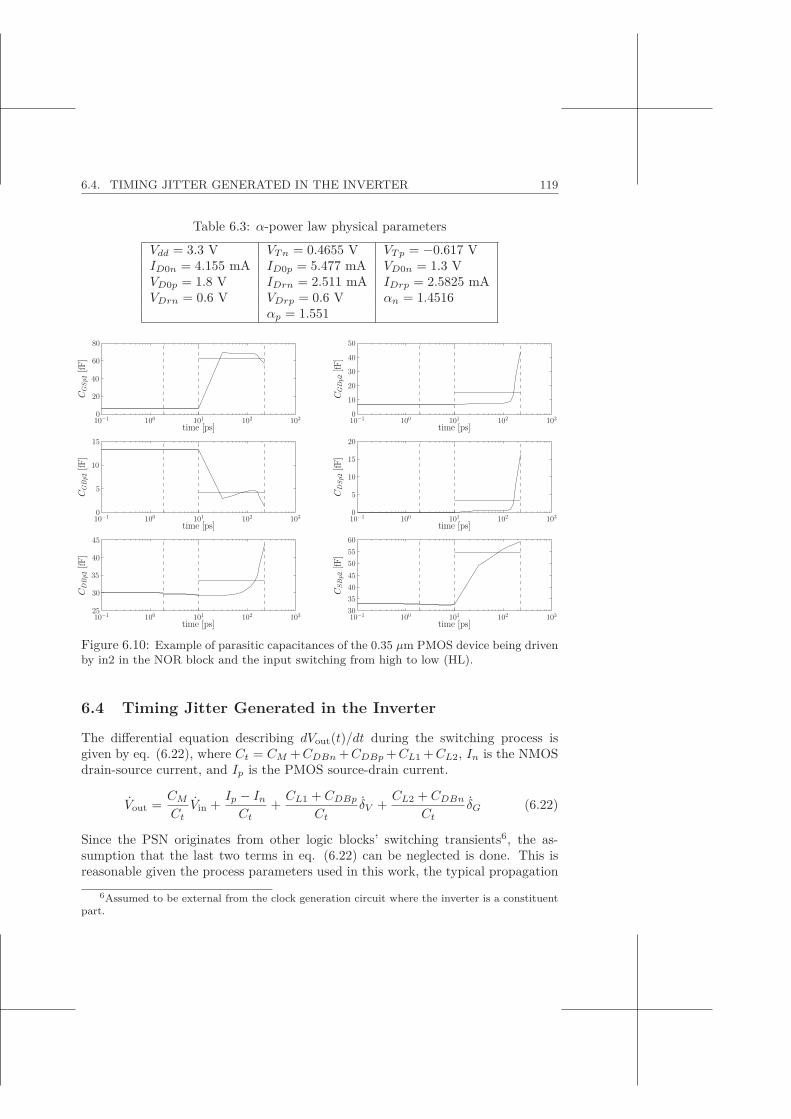
6.4. TIMING JITTER GENERATED IN THE INVERTER 119
Table 6.3: α-power law physical parameters
Vdd = 3.3 V VTn = 0.4655 V VTp = −0.617 VID0n = 4.155 mA ID0p = 5.477 mA VD0n = 1.3 VVD0p = 1.8 V IDrn = 2.511 mA IDrp = 2.5825 mAVDrn = 0.6 V VDrp = 0.6 V αn = 1.4516
αp = 1.551
time [ps]
CG
Sp2
[fF]
time [ps]
CG
Dp2
[fF]
time [ps]
CG
Bp2
[fF]
time [ps]
CD
Sp2
[fF]
time [ps]
CD
Bp2
[fF]
time [ps]
CSB
p2[fF
]
10−1 100 101 102 10310−1 100 101 102 103
10−1 100 101 102 10310−1 100 101 102 103
10−1 100 101 102 10310−1 100 101 102 103
30354045505560
25
30
35
40
45
0
5
10
15
20
0
5
10
15
0
10
20
30
40
50
0
20
40
60
80
Figure 6.10: Example of parasitic capacitances of the 0.35 μm PMOS device being drivenby in2 in the NOR block and the input switching from high to low (HL).
6.4 Timing Jitter Generated in the Inverter
The differential equation describing dVout(t)/dt during the switching process isgiven by eq. (6.22), where Ct = CM +CDBn +CDBp +CL1 +CL2, In is the NMOSdrain-source current, and Ip is the PMOS source-drain current.
Vout =CM
CtVin +
Ip − InCt
+CL1 + CDBp
CtδV +
CL2 + CDBn
CtδG (6.22)
Since the PSN originates from other logic blocks’ switching transients6, the as-sumption that the last two terms in eq. (6.22) can be neglected is done. This isreasonable given the process parameters used in this work, the typical propagation
6Assumed to be external from the clock generation circuit where the inverter is a constituentpart.

120 CHAPTER 6. JITTER GENERATION IN NONOVERLAPPING CGCS
time of an inverter in either of these processes (∼ 80 ps and ∼ 30 ps for the twoprocesses), and the steep input slope (τ0.35μm = 10 ps and τ0.18μm = 5 ps).
During a switching transient, the NMOS and PMOS transistors traverse severaloperation regions. For an input low-high transition, the transistors go through thefollowing regions7.
1) t ∈ [0, tn]: NMOS off, PMOS rev.
2) t ∈ [tn,min{tp, τ}]: NMOS sat, PMOS rev.
3) t ∈ [min{tp, τ},max{tp, τ}]: NMOS sat, PMOS off/rev.
4) t ∈ [max{tp, τ},min{tt, tend}]: NMOS sat, PMOS off.
5) t ∈ [min{tt, tend}, tend]: NMOS tri, PMOS off.
tn denotes the time when the NMOS turns on, i.e. when Vin(t) − δG(t) = VTn.Similarly, tp denotes the time when the PMOS transistor turns off, i.e. whenVout(t) − Vin(t) < −VTp. tt denotes the time when the NMOS transistor enterstriode region, i.e. when Vout(t) − δG(t) < V ′
D0n(t). tend denotes the time whenVout(t) crosses Vdd/2 and represents the time instant of complete propagation tothe following stage. The various time and operating regions are shown in figure6.11 where the input/output characteristic was simulated without PSN. It shouldbe noted that the rightmost region does not represent region 5 since, in the upperfigure, the tend point has already passed whereas in the lower figure, tend is later thanwhen the PMOS transistor goes into triode region8. Clearly, the region boundariesare dependent on the power-supply noise which means an analytical treatment isnot possible. This is because if the region boundary is not fixed, the differentialequation (6.22) is not unique. However, by making the approximations tp ≈ τ ,tt ≈ tend, and {δG(t), δV (t)} ≈ {δG, δV } for t ∈ [0, τ ], it is possible to reduce thenumber of regions to three:
1) t ∈ [0, tn]: NMOS off, PMOS rev.
2) t ∈ [tn, τ ]: NMOS sat, PMOS rev.
3) t ∈ [τ, tend]: NMOS sat, PMOS off.
These are the regions for an input LH transition. The regions for a HL transitionare obtained, as before, by substituting NMOS with PMOS and vice versa and nwith p. δG and δV are defined as the time averages, from 0 to τ , of δG(t) and δV (t)respectively. Because of the approximations mentioned, tn will henceforth denotethe time when the NMOS turns on during a LH transition, and tp will denote the
7For an input high-low transition, simply substitute NMOS with PMOS and vice versa and nwith p in the time notation.
8The region boundary of the rightmost time region in figure 6.11 represents t = tt and indicatesthat the charging/discharging transistor enters triode region.

6.4. TIMING JITTER GENERATED IN THE INVERTER 121
time [ps]
V[Vdd]
LH, δG = δV = 0 V
time [ps]
V[Vdd]
HL, δG = δV = 0 V
VinVout (SPICE)
VinVout (SPICE)
0 20 40 60 80 100 120 140 160 180 200
0 20 40 60 80 100 120 140 160 180 200
0
0.5
1
0
0.5
1
Figure 6.11: Example of 0.35μm inverter input/output characteristic. Both the inputLH and HL transitions are shown.
time when the PMOS turns on during a HL transition. These time instants areobtained from the assumption of trapezoidal input signal and the theorem of similartriangles.
tn =(VTn + δG
Vdd
)τ tp = −
(VTp + δVVdd
)τ (6.23)
6.4.1 Region 1: t ∈ [0, t(n,p)]
During region 1 (LH), the NMOS transistor is off while the PMOS transistor oper-ates in reverse region due to the overshoot. For the HL case, the PMOS transistoris off while the NMOS transistor is in reverse mode due to the undershoot. Themagnitude of the overshoot/undershoot depends on the steepness of the input sig-nal slope and the parasitic capacitance CM . The differential equations describingthe output voltages for the two cases are obtained by combining eqs. (6.22), (6.9),and (6.10).
V LHout ≈ cm1Vin − Krp
Ct1(Vout − Vin + VTp)αp/2(Vout − Vdd − δV ) (6.24)
V HLout ≈ cm1Vin +
Krn
Ct1(Vin − Vout − VTn)αn/2(δG − Vout) (6.25)
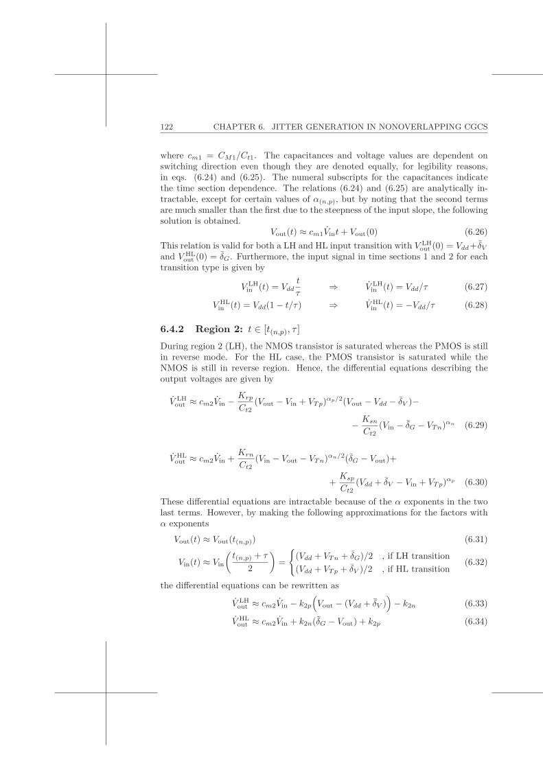
122 CHAPTER 6. JITTER GENERATION IN NONOVERLAPPING CGCS
where cm1 = CM1/Ct1. The capacitances and voltage values are dependent onswitching direction even though they are denoted equally, for legibility reasons,in eqs. (6.24) and (6.25). The numeral subscripts for the capacitances indicatethe time section dependence. The relations (6.24) and (6.25) are analytically in-tractable, except for certain values of α(n,p), but by noting that the second termsare much smaller than the first due to the steepness of the input slope, the followingsolution is obtained.
Vout(t) ≈ cm1Vint+ Vout(0) (6.26)This relation is valid for both a LH and HL input transition with V LH
out (0) = Vdd+δVand V HL
out (0) = δG. Furthermore, the input signal in time sections 1 and 2 for eachtransition type is given by
V LHin (t) = Vdd
t
τ⇒ V LH
in (t) = Vdd/τ (6.27)
V HLin (t) = Vdd(1 − t/τ) ⇒ V HL
in (t) = −Vdd/τ (6.28)
6.4.2 Region 2: t ∈ [t(n,p), τ ]
During region 2 (LH), the NMOS transistor is saturated whereas the PMOS is stillin reverse mode. For the HL case, the PMOS transistor is saturated while theNMOS is still in reverse region. Hence, the differential equations describing theoutput voltages are given by
V LHout ≈ cm2Vin − Krp
Ct2(Vout − Vin + VTp)αp/2(Vout − Vdd − δV )−
− Ksn
Ct2(Vin − δG − VTn)αn (6.29)
V HLout ≈ cm2Vin +
Krn
Ct2(Vin − Vout − VTn)αn/2(δG − Vout)+
+Ksp
Ct2(Vdd + δV − Vin + VTp)αp (6.30)
These differential equations are intractable because of the α exponents in the twolast terms. However, by making the following approximations for the factors withα exponents
Vout(t) ≈ Vout(t(n,p)) (6.31)
Vin(t) ≈ Vin
(t(n,p) + τ
2
)=
{(Vdd + VTn + δG)/2 , if LH transition(Vdd + VTp + δV )/2 , if HL transition
(6.32)
the differential equations can be rewritten as
V LHout ≈ cm2Vin − k2p
(Vout − (Vdd + δV )
)− k2n (6.33)
V HLout ≈ cm2Vin + k2n(δG − Vout) + k2p (6.34)

6.4. TIMING JITTER GENERATED IN THE INVERTER 123
where
kLH2p =
Krp
Ct2
(Vout(tn) − Vdd + VTn + δG
2+ VTp
)αp2
=
=Krp
Ct2
(Vdd
2−
(12− cm1
)(VTn + δG) + δV + VTp
)αp2
(6.35)
kLH2n =
Ksn
Ct2
(Vdd − δG − VTn
2
)αn
kHL2p = −Ksp
Ct2
(Vdd + δV + VTp
2
)αp
(6.36)
kHL2n =
Krn
Ct2
(Vdd + VTp + δV
2− Vout(tp) − VTn
)αn2
=
=Krn
Ct2
(Vdd
2+
(12− cm1
)(VTp + δV ) − δG − VTn
)αn2
(6.37)
Both eqs. (6.33) and (6.34) are straightforward to solve.
V LHout (t) ≈ Vout(tn)e−k2p(t−tn)+
(cm2
Vink2p
+Vdd+δV − k2n
k2p
)(1−e−k2p(t−tn)
)(6.38)
V HLout (t) ≈ Vout(tp)e−k2n(t−tp) −
(cm2
Vink2n
− δG − k2p
k2n
)(1 − e−k2n(t−tp)
)(6.39)
For the 0.35μm process parameters and both switching directions,
max{k2(n,p)(t− t(n,p))} < max{k2(n,p)τ} 1 , for |{δG, δV }| ≤ 0.1Vdd (6.40)
Hence, the approximation ex ≈ 1+x may be used without too much loss of accuracy.Therefore, the solutions can be written
V LHout (t) ≈
(cm2Vin +(Vdd + δV )k2p−k2n
)(t−tn)+Vout(tn)
(1−k2p(t−tn)
)(6.41)
V HLout (t) ≈
(cm2Vin + δGk2n − k2p
)(t− tp) + Vout(tp)
(1 − k2n(t− tp)
)(6.42)
Eq. (6.26) gives Vout(tn) and Vout(tp) which means the region 2 voltages are givenby
V LHout (t) ≈
(cm2Vin − k2n
)(t− tn) + cm1Vintn
(1 − k2p(t− tn)
)+ Vdd + δV (6.43)
V HLout (t) ≈
(cm2Vin − k2p
)(t− tp) + cm1Vintp
(1 − k2n(t− tp)
)+ δG (6.44)
124 CHAPTER 6. JITTER GENERATION IN NONOVERLAPPING CGCS
6.4.3 Region 3: t ∈ [τ, tend]
In the third region (LH), the NMOS is saturated while the PMOS is approximatedas off. For the HL scenario, the PMOS is saturated while the NMOS is approxi-mated as off. Furthermore, the input signal is constant. Therefore, the differentialequations describing the output voltages are given by
V LHout ≈ −Ksn
Ct3(Vdd − δG − VTn)αn (6.45)
V HLout ≈ Ksp
Ct3(Vdd + δV + VTp)αp (6.46)
By approximating the power-supply noise {δV (t), δG(t)} with an average from t = τto t = tend,ideal, where Vout(tend,ideal) = Vdd/2 in an environment without PSN, thesolution becomes
Vout(t) ≈ Vout(τ) + k3(t− τ) (6.47)
where
kLH3 = −Ksn
Ct3(Vdd − δG2 − VTn)αn (6.48)
kHL3 =
Ksp
Ct3(Vdd + δV 2 + VTp)αp (6.49)
Figure 6.12 shows how well the closed-form expressions of Vout(t) fit with the SPICEsimulation results and also includes the numerical solution to eq. (6.22) whereall five regions are considered. Clearly, the CFEs accurately predict the invertertransition behavior (δG = δV = 0 V).
6.4.4 Propagation DelayThe propagation delay can be found by setting eq. (6.47) equal to Vdd/2 and solvefor t = tend = tpd + τ/2.
Vout(τ) + k3(tend − τ) = Vdd/2 ⇒ tpd =τ
2+
1k3
(Vdd/2− Vout(τ)
)(6.50)
Expanding the terms Vout(τ) with the help of eqs. (6.43) and (6.44) gives
tLHpd ≈ τ
2+Vdd/2 + δV + (cm2Vin − k2n)(τ − tn) + cm1Vintn
(1 − k2p(τ − tn)
)Ksn(Vdd − δG2 − VTn)αn/Ct3
(6.51)
tHLpd ≈ τ
2+Vdd/2 − δG − (cm2Vin − k2p)(τ − tp) − cm1Vintp
(1 − k2n(τ − tp)
)Ksp(Vdd + δV 2 + VTp)αp/Ct3
(6.52)
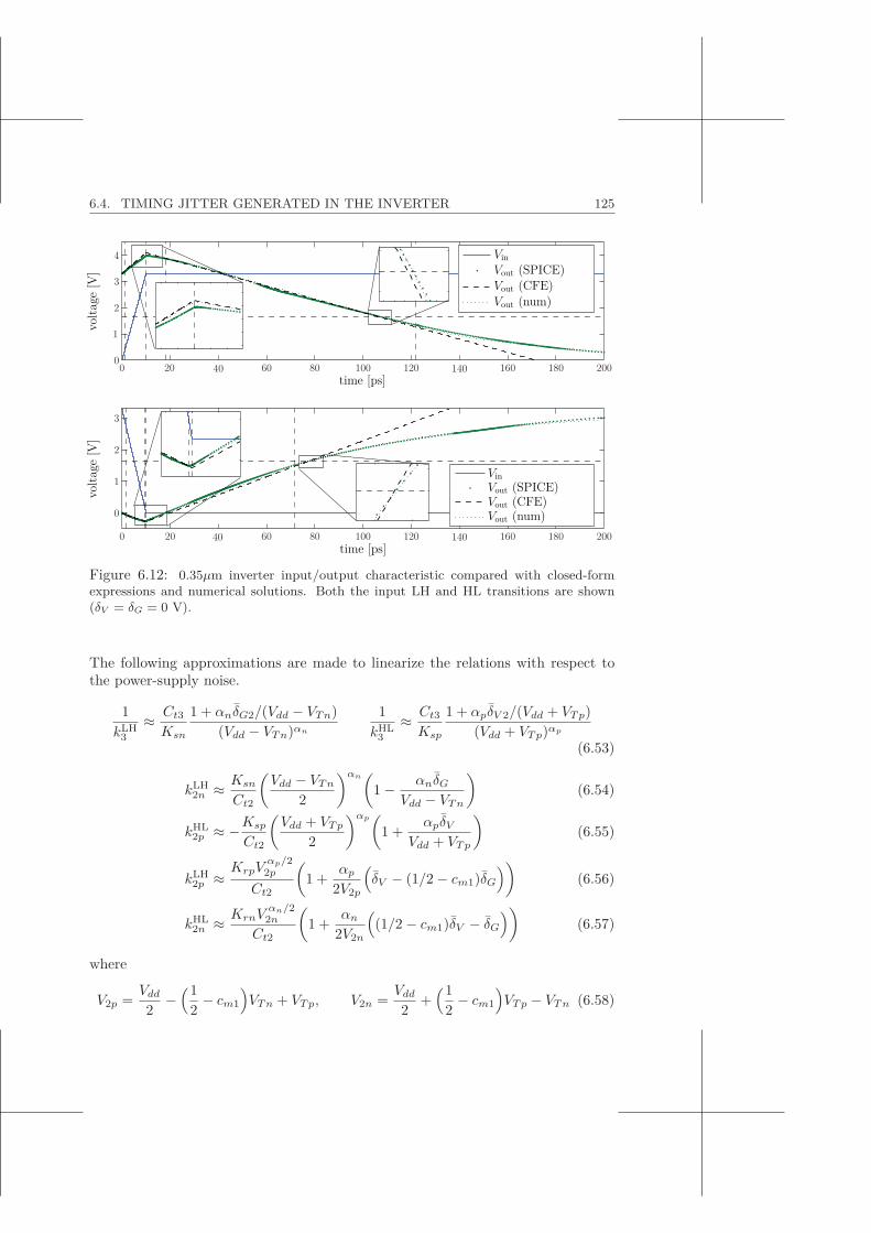
6.4. TIMING JITTER GENERATED IN THE INVERTER 125
time [ps]
volta
ge[V
]
time [ps]
volta
ge[V
]
VinVout (SPICE)Vout (CFE)Vout (num)
VinVout (SPICE)Vout (CFE)Vout (num)
0 20 40 60 80 100 120 140 160 180 200
0 20 40 60 80 100 120 140 160 180 200
0
1
2
3
0
1
2
3
4
Figure 6.12: 0.35μm inverter input/output characteristic compared with closed-formexpressions and numerical solutions. Both the input LH and HL transitions are shown(δV = δG = 0 V).
The following approximations are made to linearize the relations with respect tothe power-supply noise.
1kLH3
≈ Ct3
Ksn
1 + αnδG2/(Vdd − VTn)(Vdd − VTn)αn
1kHL3
≈ Ct3
Ksp
1 + αpδV 2/(Vdd + VTp)(Vdd + VTp)αp
(6.53)
kLH2n ≈ Ksn
Ct2
(Vdd − VTn
2
)αn(
1 − αnδGVdd − VTn
)(6.54)
kHL2p ≈ −Ksp
Ct2
(Vdd + VTp
2
)αp(
1 +αpδV
Vdd + VTp
)(6.55)
kLH2p ≈ KrpV
αp/22p
Ct2
(1 +
αp
2V2p
(δV − (1/2 − cm1)δG
))(6.56)
kHL2n ≈ KrnV
αn/22n
Ct2
(1 +
αn
2V2n
((1/2 − cm1)δV − δG
))(6.57)
where
V2p =Vdd
2−
(12− cm1
)VTn + VTp, V2n =
Vdd
2+
(12− cm1
)VTp − VTn (6.58)
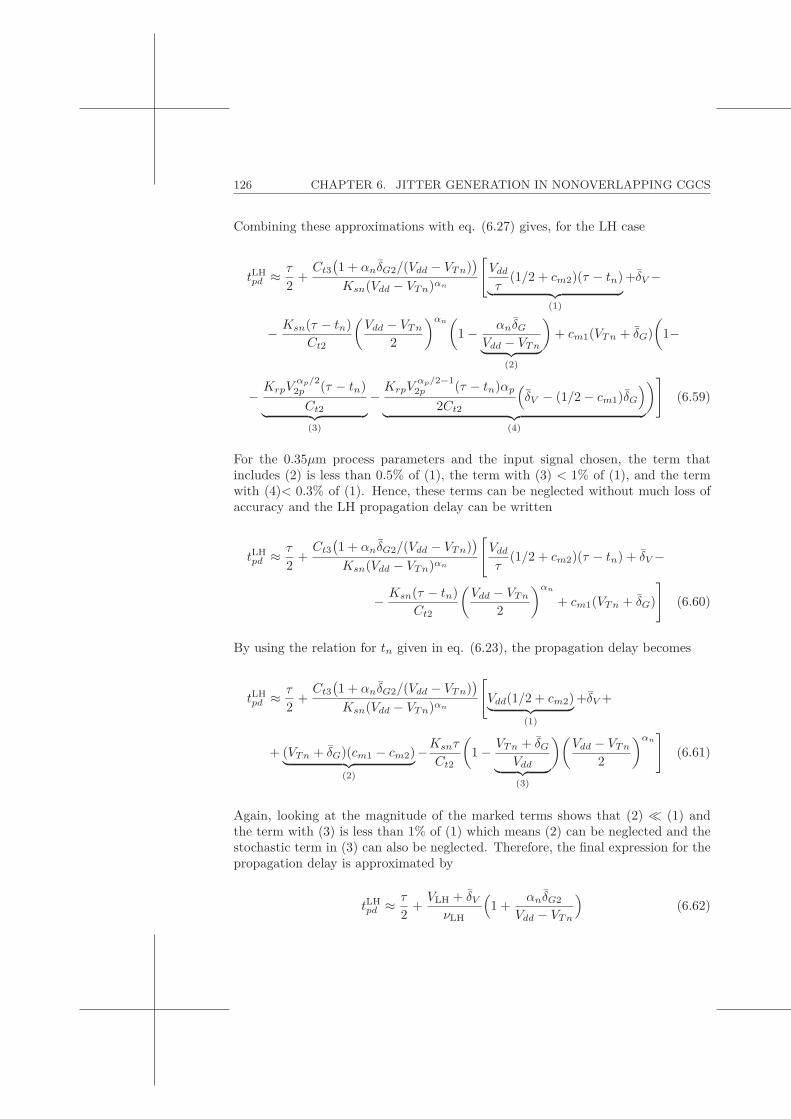
126 CHAPTER 6. JITTER GENERATION IN NONOVERLAPPING CGCS
Combining these approximations with eq. (6.27) gives, for the LH case
tLHpd ≈ τ
2+Ct3
(1 + αnδG2/(Vdd − VTn)
)Ksn(Vdd − VTn)αn
[Vdd
τ(1/2 + cm2)(τ − tn)︸ ︷︷ ︸
(1)
+δV −
− Ksn(τ − tn)Ct2
(Vdd − VTn
2
)αn(
1 − αnδGVdd − VTn︸ ︷︷ ︸
(2)
)+ cm1(VTn + δG)
(1−
− KrpVαp/22p (τ − tn)Ct2︸ ︷︷ ︸(3)
− KrpVαp/2−12p (τ − tn)αp
2Ct2
(δV − (1/2 − cm1)δG
)︸ ︷︷ ︸
(4)
)](6.59)
For the 0.35μm process parameters and the input signal chosen, the term thatincludes (2) is less than 0.5% of (1), the term with (3) < 1% of (1), and the termwith (4)< 0.3% of (1). Hence, these terms can be neglected without much loss ofaccuracy and the LH propagation delay can be written
tLHpd ≈ τ
2+Ct3
(1 + αnδG2/(Vdd − VTn)
)Ksn(Vdd − VTn)αn
[Vdd
τ(1/2 + cm2)(τ − tn) + δV −
− Ksn(τ − tn)Ct2
(Vdd − VTn
2
)αn
+ cm1(VTn + δG)
](6.60)
By using the relation for tn given in eq. (6.23), the propagation delay becomes
tLHpd ≈ τ
2+Ct3
(1 + αnδG2/(Vdd − VTn)
)Ksn(Vdd − VTn)αn
[Vdd(1/2 + cm2)︸ ︷︷ ︸
(1)
+δV +
+ (VTn + δG)(cm1 − cm2)︸ ︷︷ ︸(2)
−Ksnτ
Ct2
(1 − VTn + δG
Vdd︸ ︷︷ ︸(3)
)(Vdd − VTn
2
)αn]
(6.61)
Again, looking at the magnitude of the marked terms shows that (2) (1) andthe term with (3) is less than 1% of (1) which means (2) can be neglected and thestochastic term in (3) can also be neglected. Therefore, the final expression for thepropagation delay is approximated by
tLHpd ≈ τ
2+VLH + δVνLH
(1 +
αnδG2
Vdd − VTn
)(6.62)

6.4. TIMING JITTER GENERATED IN THE INVERTER 127
where
VLH = Vdd
(12
+ cm2
)− Ksnτ
Ct2
(Vdd − VTn)αn+1
2αnVdd(6.63)
νLH =Ksn
Ct3(Vdd − VTn)αn (6.64)
The deduction of the propagation delay in the case of a HL transition follows thesame pattern. Using eqs. (6.28) and (6.23) together with (6.52) gives the followingpropagation delay expression.
tHLpd ≈ τ
2+Ct3
(1 − αpδV 2/(Vdd + VTp)
)Ksp(Vdd + VTp)αp
[Vdd(1/2 + cm2)︸ ︷︷ ︸
(1)
−δG+
+ (VTp + δV )(cm1 − cm2)︸ ︷︷ ︸(2)
−Kspτ
Ct2
(1 +
VTp + δVVdd︸ ︷︷ ︸(3)
)(Vdd + VTp
2
)αp]
(6.65)
The term (2) is much smaller than (1) and the stochastic term in (3) is also in-significant compared to (1). Therefore, the propagation delay can be written
tHLpd ≈ τ
2+VHL − δGνHL
(1 − αpδV 2
Vdd + VTp
)(6.66)
where
VHL = Vdd
(12
+ cm2
)− Kspτ
Ct2
(Vdd + VTp)αp+1
2αpVdd(6.67)
νHL =Ksp
Ct3(Vdd + VTp)αp (6.68)
Figure 6.13 shows the LH and HL propagation delay variations, Δtpd = tpd(δG, δV )−tpd(0, 0), for static shifts in the power and ground potentials. The closed-form ex-pressions show good agreement with the SPICE simulations except for large shiftsin the supply voltage. For these cases, the region approximation from five regions tothree is the main source of error. For the LH transition, the approximation that att = τ the PMOS transistor turns off is the primary source of deviation (see fig. 6.12top). For the HL transition, the approximation that the PMOS transistor remainssaturated until t = tend is the main error contributor (see fig. 6.12 bottom).
6.4.5 Timing JitterTo deduce the jitter rms induced by power-supply noise, the variance of eqs. (6.62)and (6.66) is formed.
σ2j = V{tpd} = E{t2pd} − E2{tpd} (6.69)
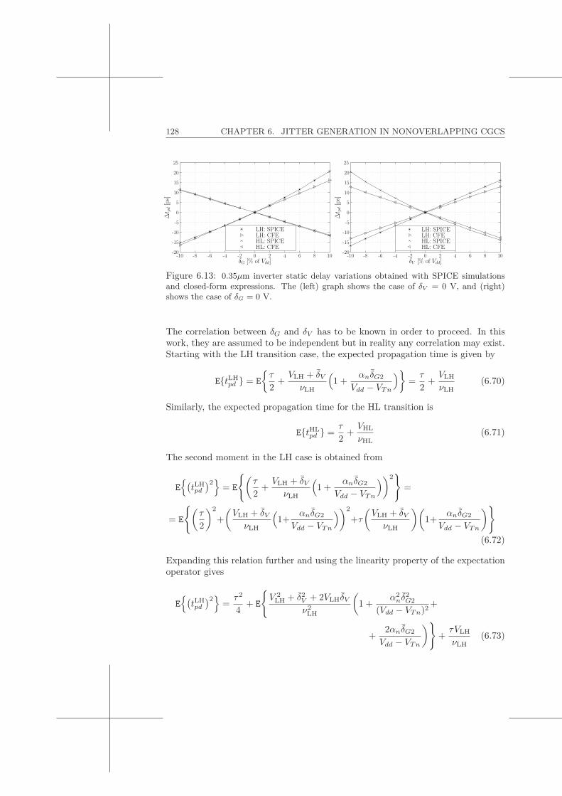
128 CHAPTER 6. JITTER GENERATION IN NONOVERLAPPING CGCS
δG [% of Vdd]
Δt p
d[p
s]
LH: SPICELH: CFEHL: SPICEHL: CFE
-10 -8 -6 -4 -2 0 2 4 6 8 10-20
-15
-10
-5
0
5
10
15
20
25
δV [% of Vdd]
Δt p
d[p
s]
LH: SPICELH: CFEHL: SPICEHL: CFE
-10 -8 -6 -4 -2 0 2 4 6 8 10-20
-15
-10
-5
0
5
10
15
20
25
Figure 6.13: 0.35μm inverter static delay variations obtained with SPICE simulationsand closed-form expressions. The (left) graph shows the case of δV = 0 V, and (right)shows the case of δG = 0 V.
The correlation between δG and δV has to be known in order to proceed. In thiswork, they are assumed to be independent but in reality any correlation may exist.Starting with the LH transition case, the expected propagation time is given by
E{tLHpd } = E
{τ
2+VLH + δVνLH
(1 +
αnδG2
Vdd − VTn
)}=τ
2+VLHνLH
(6.70)
Similarly, the expected propagation time for the HL transition is
E{tHLpd } =
τ
2+VHLνHL
(6.71)
The second moment in the LH case is obtained from
E{(tLHpd
)2}
= E
{(τ
2+VLH + δVνLH
(1 +
αnδG2
Vdd − VTn
))2}
=
= E
{(τ
2
)2
+(VLH + δVνLH
(1+
αnδG2
Vdd − VTn
))2
+τ(VLH + δVνLH
)(1+
αnδG2
Vdd − VTn
)}(6.72)
Expanding this relation further and using the linearity property of the expectationoperator gives
E{(tLHpd
)2}
=τ2
4+ E
{V 2
LH + δ2V + 2VLHδVν2
LH
(1 +
α2nδ
2G2
(Vdd − VTn)2+
+2αnδG2
Vdd − VTn
)}+τVLHνLH
(6.73)
6.4. TIMING JITTER GENERATED IN THE INVERTER 129
By noting that σGσV σGVLH, the result becomes
E{(tLHpd
)2}≈ τ2
4+τVLHνLH
+V 2
LHν2
LH+σ2
V
ν2LH
+α2
nσ2GV
2LH
ν2LH(Vdd − VTn)2
(6.74)
where
V{δ(V,G)(t)} = E{δ2(V,G)(t)} = σ2(V,G) ≈ V{δ(V,G)} ≈ V{δ(V 2,G2)} (6.75)
The motivation behind the approximations in eq. (6.75) is twofold. First, thecentral limit theorem, described in chapter 4, says that the variance of an ensembleaverage is the sample variance divided by the ensemble size if the samples areindependent. However, the time average is not the same as an ensemble average.The lengths of the time sections are short enough to typically hold only a few τPSN(for realistic τPSN) so the number of power-supply noise samples is low. Second,the intermediate power-supply noise values do not contribute to the reduction inthe time average variance since they are linear combinations of two independentsamples, i.e. they lack the independence property. Thus, the variance of the averagepower-supply noise within one time section can be approximated by the varianceof the power-supply noise itself.
For the HL case, the second moment is given by
E{(tHLpd
)2}
=τ2
4+τVHLνHL
+ E
{V 2
HL + δ2G + 2VHLδGν2
HL
(1 +
α2pδ
2V 2
(Vdd + VTp)2+
+2αpδV 2
Vdd + VTp
)}≈ τ2
4+τVHLνHL
+V 2
HLν2
HL+
σ2G
ν2HL
+α2
pσ2V V
2HL
ν2HL(Vdd + VTp)2
(6.76)
Hence, the rms timing jitter for the LH and HL transitions are given by
σ2j,LH ≈ σ2
V
ν2LH
+α2
nσ2G
(Vdd − VTn)2
(VLHνLH
)2
(6.77)
σ2j,HL ≈ σ2
G
ν2HL
+α2
pσ2V
(Vdd + VTp)2
(VHLνHL
)2
(6.78)
The simulation results where the variations in propagation delay have been obtainedare shown in figure 6.14. Here, histograms of the power-supply noise togetherwith propagation delay deviations are shown. The Δtpd histograms resemble theGaussian shape of the PSN which supports the conclusions of eqs. (6.62) and(6.66), that the relation between Δtpd and the supply shift is linear9. This linearrelationship is confirmed in figure 6.15 where eqs. (6.77) and (6.78) are comparedwith the simulations based on the 0.35μm process parameters. Clearly, the closed-form expressions are very accurate and correspond well with the simulations. The
9This linearity has been assumed in earlier work from other authors, such as [79], but has notbeen proved earlier according to the author’s knowledge.

130 CHAPTER 6. JITTER GENERATION IN NONOVERLAPPING CGCS
#of
sam
ples
δV [V]
#of
sam
ples
δG [V]
#of
sam
ples
ΔtLHpd [ps]
#of
sam
ples
ΔtHLpd [ps]
-30 -20 -10 0 10 20 30-30 -20 -10 0 10 20 30
-0.5 -0.4 -0.3 -0.2 -0.1 0 0.1 0.2 0.3 0.4 0.5-0.5 -0.4 -0.3 -0.2 -0.1 0 0.1 0.2 0.3 0.4 0.5
0
10
20
30
40
50
60
70
80
0
10
20
30
40
50
60
70
80
0
100
200
300
400
500
600
700
0
100
200
300
400
500
600
700
Figure 6.14: Histograms of δV and δG and the propagation delay deviations ΔtLHpd and
ΔtHLpd .
0.18μm simulation results are shown for reference indicating how the jitter rmsevolves with the process technology. For the 0.35μm simulations, τPSN = 250 ps,and for the 0.18μm simulations, τPSN = 125 ps.
In order to minimize the timing jitter induced by power-supply noise, the factorV(LH,HL) should be minimized and the factor ν(LH,HL) should be maximized. Thiscorresponds to minimizing the inverter’s propagation delay as given by eqs. (6.62)and (6.66). Comparing these two equations with eq. (6.50) indicates that V(LH,HL)corresponds to the factor |Vdd/2−Vout(τ)|, i.e. a measure of overshoot/undershoot,and ν(LH,HL) corresponds to k3, i.e. the discharge/charge voltage slope in region3. Hence, the propagation delay is minimized when the overshoot/undershoot isminimized and the voltage slope in the discharge/charge region is maximized. Theseare conflicting requirements since the first is achieved through minimizing parasiticcapacitance, i.e. minimizing transistor size, whereas the second requirement isachieved through maximizing drain-source current, i.e. maximizing the transistorsize. However, increasing the transistor size has a larger impact on the drain-source current than the overshoot/undershoot which means that the benefit of alarge transistor size outweighs the drawback of larger overshoot/undershoot.
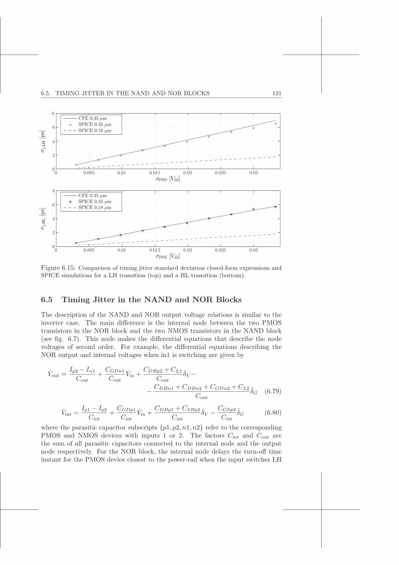
6.5. TIMING JITTER IN THE NAND AND NOR BLOCKS 131
σPSN [Vdd]
σj,
LH[p
s]
σPSN [Vdd]
σj,
HL
[ps]
CFE 0.35 μmSPICE 0.35 μmSPICE 0.18 μm
CFE 0.35 μmSPICE 0.35 μmSPICE 0.18 μm
0 0.005 0.01 0.015 0.02 0.025 0.03
0 0.005 0.01 0.015 0.02 0.025 0.03
0
2
4
6
8
0
2
4
6
8
Figure 6.15: Comparison of timing jitter standard deviation closed-form expressions andSPICE simulations for a LH transition (top) and a HL transition (bottom).
6.5 Timing Jitter in the NAND and NOR Blocks
The description of the NAND and NOR output voltage relations is similar to theinverter case. The main difference is the internal node between the two PMOStransistors in the NOR block and the two NMOS transistors in the NAND block(see fig. 6.7). This node makes the differential equations that describe the nodevoltages of second order. For example, the differential equations describing theNOR output and internal voltages when in1 is switching are given by
Vout =Ip2 − In1
Cout+CGDn1
CoutVin +
CDBp2 + CL1
CoutδV −
− CDBn1 + CDBn2 + CGDn2 + CL2
CoutδG (6.79)
Vint =Ip1 − Ip2
Cint+CGDp1
CintVin +
CDBp1 + CSBp2
CintδV − CGSp2
CintδG (6.80)
where the parasitic capacitor subscripts {p1, p2, n1, n2} refer to the correspondingPMOS and NMOS devices with inputs 1 or 2. The factors Cint and Cout arethe sum of all parasitic capacitors connected to the internal node and the outputnode respectively. For the NOR block, the internal node delays the turn-off timeinstant for the PMOS device closest to the power-rail when the input switches LH
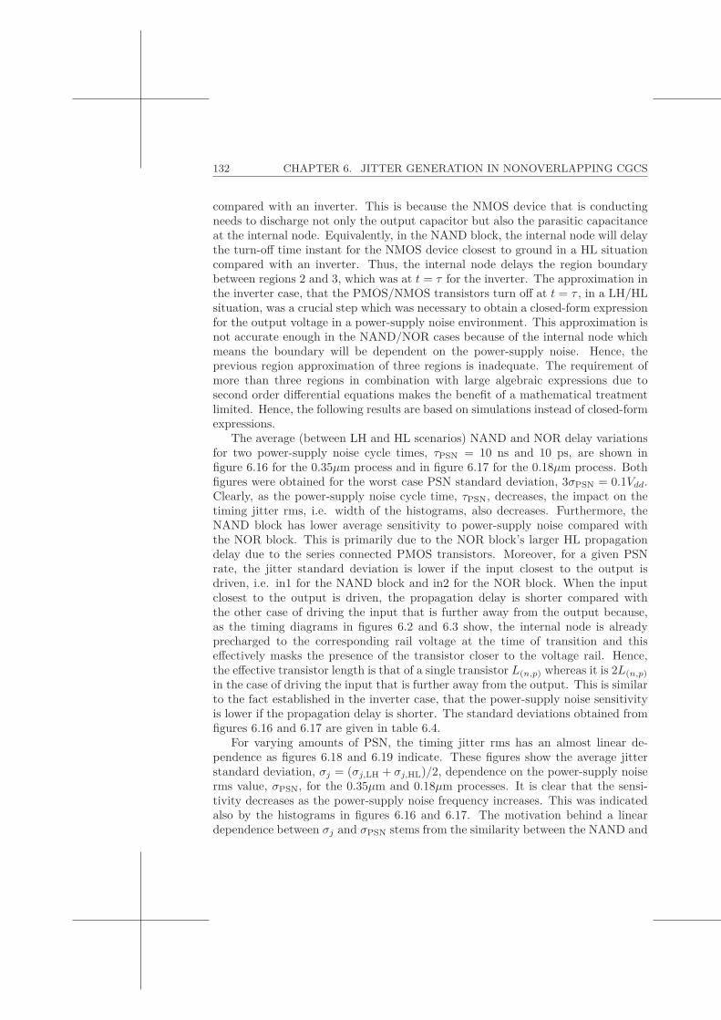
132 CHAPTER 6. JITTER GENERATION IN NONOVERLAPPING CGCS
compared with an inverter. This is because the NMOS device that is conductingneeds to discharge not only the output capacitor but also the parasitic capacitanceat the internal node. Equivalently, in the NAND block, the internal node will delaythe turn-off time instant for the NMOS device closest to ground in a HL situationcompared with an inverter. Thus, the internal node delays the region boundarybetween regions 2 and 3, which was at t = τ for the inverter. The approximation inthe inverter case, that the PMOS/NMOS transistors turn off at t = τ , in a LH/HLsituation, was a crucial step which was necessary to obtain a closed-form expressionfor the output voltage in a power-supply noise environment. This approximation isnot accurate enough in the NAND/NOR cases because of the internal node whichmeans the boundary will be dependent on the power-supply noise. Hence, theprevious region approximation of three regions is inadequate. The requirement ofmore than three regions in combination with large algebraic expressions due tosecond order differential equations makes the benefit of a mathematical treatmentlimited. Hence, the following results are based on simulations instead of closed-formexpressions.
The average (between LH and HL scenarios) NAND and NOR delay variationsfor two power-supply noise cycle times, τPSN = 10 ns and 10 ps, are shown infigure 6.16 for the 0.35μm process and in figure 6.17 for the 0.18μm process. Bothfigures were obtained for the worst case PSN standard deviation, 3σPSN = 0.1Vdd.Clearly, as the power-supply noise cycle time, τPSN, decreases, the impact on thetiming jitter rms, i.e. width of the histograms, also decreases. Furthermore, theNAND block has lower average sensitivity to power-supply noise compared withthe NOR block. This is primarily due to the NOR block’s larger HL propagationdelay due to the series connected PMOS transistors. Moreover, for a given PSNrate, the jitter standard deviation is lower if the input closest to the output isdriven, i.e. in1 for the NAND block and in2 for the NOR block. When the inputclosest to the output is driven, the propagation delay is shorter compared withthe other case of driving the input that is further away from the output because,as the timing diagrams in figures 6.2 and 6.3 show, the internal node is alreadyprecharged to the corresponding rail voltage at the time of transition and thiseffectively masks the presence of the transistor closer to the voltage rail. Hence,the effective transistor length is that of a single transistor L(n,p) whereas it is 2L(n,p)
in the case of driving the input that is further away from the output. This is similarto the fact established in the inverter case, that the power-supply noise sensitivityis lower if the propagation delay is shorter. The standard deviations obtained fromfigures 6.16 and 6.17 are given in table 6.4.
For varying amounts of PSN, the timing jitter rms has an almost linear de-pendence as figures 6.18 and 6.19 indicate. These figures show the average jitterstandard deviation, σj = (σj,LH + σj,HL)/2, dependence on the power-supply noiserms value, σPSN, for the 0.35μm and 0.18μm processes. It is clear that the sensi-tivity decreases as the power-supply noise frequency increases. This was indicatedalso by the histograms in figures 6.16 and 6.17. The motivation behind a lineardependence between σj and σPSN stems from the similarity between the NAND and

6.5. TIMING JITTER IN THE NAND AND NOR BLOCKS 133
#of
sam
ples
(a) NOR Δtpd [ps]
#of
sam
ples
(b) NAND Δtpd [ps]
#of
sam
ples
(c) NOR Δtpd [ps]
#of
sam
ples
(d) NAND Δtpd [ps]
in1 avgin2 avg
in1 avg
in2 avg
in1 avg
in2 avg
in1 avg
in2 avg
-40 -20 0 20 40-40 -20 0 20 40
-40 -20 0 20 40-40 -20 0 20 40
0
50
100
150
200
0
50
100
150
200
0
50
100
150
0
20
40
60
80
Figure 6.16: 0.35μm propagation delay deviation histograms for (a,b) τPSN = 10 ns, (c,d)τPSN = 10 ps.
#of
sam
ples
(a) NOR Δtpd [ps]
#of
sam
ples
(b) NAND Δtpd [ps]
#of
sam
ples
(c) NOR Δtpd [ps]
#of
sam
ples
(d) NAND Δtpd [ps]
in1 avg
in2 avg
in1 avg
in2 avg
in1 avg
in2 avg
in1 avg
in2 avg
-20 -10 0 10 20-20 -10 0 10 20
-20 -10 0 10 20-20 -10 0 10 20
0
50
100
150
200
0
50
100
150
200
0
20
40
60
80
100
120
0
20
40
60
80
100
Figure 6.17: 0.18μm propagation delay deviation histograms for (a,b) τPSN = 10 ns, (c,d)τPSN = 10 ps.
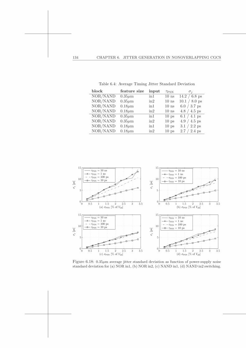
134 CHAPTER 6. JITTER GENERATION IN NONOVERLAPPING CGCS
Table 6.4: Average Timing Jitter Standard Deviation
block feature size input τPSN σj
NOR/NAND 0.35μm in1 10 ns 14.2 / 6.8 psNOR/NAND 0.35μm in2 10 ns 10.1 / 8.0 psNOR/NAND 0.18μm in1 10 ns 6.0 / 3.7 psNOR/NAND 0.18μm in2 10 ns 4.8 / 4.5 psNOR/NAND 0.35μm in1 10 ps 6.1 / 4.1 psNOR/NAND 0.35μm in2 10 ps 4.9 / 4.5 psNOR/NAND 0.18μm in1 10 ps 3.1 / 2.2 psNOR/NAND 0.18μm in2 10 ps 2.7 / 2.4 ps
(a) σPSN [% of Vdd]
σj
[ps]
(b) σPSN [% of Vdd]
σj
[ps]
(c) σPSN [% of Vdd]
σj
[ps]
(d) σPSN [% of Vdd]
σj
[ps]
τPSN = 10 nsτPSN = 1 nsτPSN = 100 psτPSN = 10 ps
τPSN = 10 nsτPSN = 1 nsτPSN = 100 psτPSN = 10 ps
τPSN = 10 nsτPSN = 1 nsτPSN = 100 psτPSN = 10 ps
τPSN = 10 nsτPSN = 1 nsτPSN = 100 psτPSN = 10 ps
0 0.5 1 1.5 2 2.5 3 3.50 0.5 1 1.5 2 2.5 3 3.5
0 0.5 1 1.5 2 2.5 3 3.50 0.5 1 1.5 2 2.5 3 3.5
0
5
10
15
0
5
10
15
0
5
10
15
0
5
10
15
Figure 6.18: 0.35μm average jitter standard deviation as function of power-supply noisestandard deviation for (a) NOR in1, (b) NOR in2, (c) NAND in1, (d) NAND in2 switching.
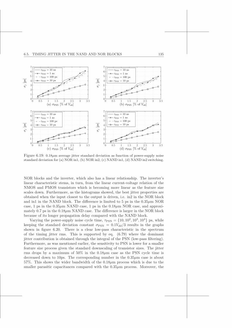
6.5. TIMING JITTER IN THE NAND AND NOR BLOCKS 135
(a) σPSN [% of Vdd]
σj
[ps]
(b) σPSN [% of Vdd]
σj
[ps]
(c) σPSN [% of Vdd]
σj
[ps]
(d) σPSN [% of Vdd]
σj
[ps]
τPSN = 10 nsτPSN = 1 nsτPSN = 100 psτPSN = 10 ps
τPSN = 10 nsτPSN = 1 nsτPSN = 100 psτPSN = 10 ps
τPSN = 10 nsτPSN = 1 nsτPSN = 100 psτPSN = 10 ps
τPSN = 10 nsτPSN = 1 nsτPSN = 100 psτPSN = 10 ps
0 0.5 1 1.5 2 2.5 3 3.50 0.5 1 1.5 2 2.5 3 3.5
0 0.5 1 1.5 2 2.5 3 3.50 0.5 1 1.5 2 2.5 3 3.5
01234567
01234567
01234567
01234567
Figure 6.19: 0.18μm average jitter standard deviation as function of power-supply noisestandard deviation for (a) NOR in1, (b) NOR in2, (c) NAND in1, (d) NAND in2 switching.
NOR blocks and the inverter, which also has a linear relationship. The inverter’slinear characteristic stems, in turn, from the linear current-voltage relation of theNMOS and PMOS transistors which is becoming more linear as the feature sizescales down. Furthermore, as the histograms showed, the best jitter properties areobtained when the input closest to the output is driven, i.e. in2 in the NOR blockand in1 in the NAND block. The difference is limited to 5 ps in the 0.35μm NORcase, 1 ps in the 0.35μm NAND case, 1 ps in the 0.18μm NOR case, and approxi-mately 0.7 ps in the 0.18μm NAND case. The difference is larger in the NOR blockbecause of its longer propagation delay compared with the NAND block.
Varying the power-supply noise cycle time, τPSN = {10, 102, 103, 104} ps, whilekeeping the standard deviation constant σPSN = 0.1Vdd/3 results in the graphsshown in figure 6.20. There is a clear low-pass characteristic in the spectrumof the timing jitter rms. This is supported by eq. (6.79) where the dominantjitter contribution is obtained through the integral of the PSN (low-pass filtering).Furthermore, as was mentioned earlier, the sensitivity to PSN is lower for a smallerfeature size process given the standard downscaling of transistor sizes. The jitterrms drops by a maximum of 50% in the 0.18μm case as the PSN cycle time isdecreased down to 10ps. The corresponding number in the 0.35μm case is about57%. This shows the wider bandwidth of the 0.18μm process which is due to thesmaller parasitic capacitances compared with the 0.35μm process. Moreover, the
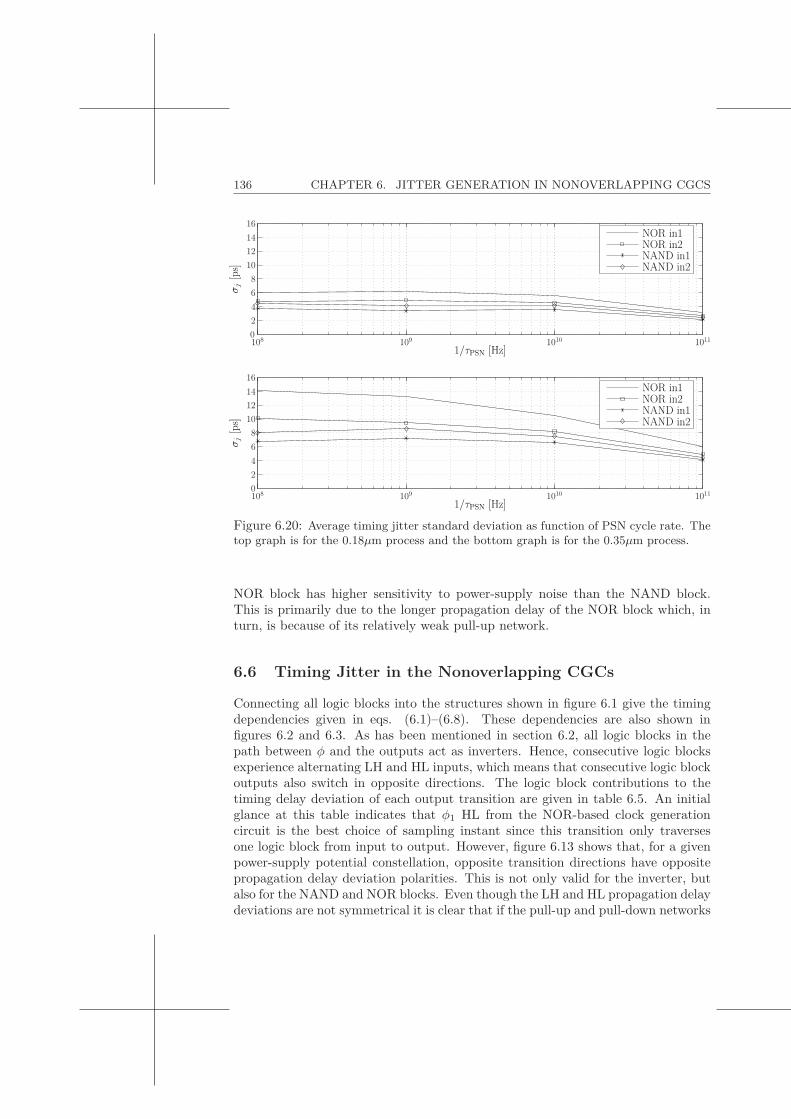
136 CHAPTER 6. JITTER GENERATION IN NONOVERLAPPING CGCS
1/τPSN [Hz]
σj
[ps]
1/τPSN [Hz]
σj
[ps]
NOR in1NOR in2NAND in1NAND in2
NOR in1NOR in2NAND in1NAND in2
108 109 1010 1011
108 109 1010 1011
02468
10121416
02468
10121416
Figure 6.20: Average timing jitter standard deviation as function of PSN cycle rate. Thetop graph is for the 0.18μm process and the bottom graph is for the 0.35μm process.
NOR block has higher sensitivity to power-supply noise than the NAND block.This is primarily due to the longer propagation delay of the NOR block which, inturn, is because of its relatively weak pull-up network.
6.6 Timing Jitter in the Nonoverlapping CGCs
Connecting all logic blocks into the structures shown in figure 6.1 give the timingdependencies given in eqs. (6.1)–(6.8). These dependencies are also shown infigures 6.2 and 6.3. As has been mentioned in section 6.2, all logic blocks in thepath between φ and the outputs act as inverters. Hence, consecutive logic blocksexperience alternating LH and HL inputs, which means that consecutive logic blockoutputs also switch in opposite directions. The logic block contributions to thetiming delay deviation of each output transition are given in table 6.5. An initialglance at this table indicates that φ1 HL from the NOR-based clock generationcircuit is the best choice of sampling instant since this transition only traversesone logic block from input to output. However, figure 6.13 shows that, for a givenpower-supply potential constellation, opposite transition directions have oppositepropagation delay deviation polarities. This is not only valid for the inverter, butalso for the NAND and NOR blocks. Even though the LH and HL propagation delaydeviations are not symmetrical it is clear that if the pull-up and pull-down networks

6.6. TIMING JITTER IN THE NONOVERLAPPING CGCS 137
Table 6.5: Timing Uncertainty Contributions
CGC type transition contributionsNOR φ1 HL dNOR1
NOR φ1 LH dINV + dNOR2 + dd2 + dNOR1
NOR φ2 HL dINV + dNOR2
NOR φ2 LH dNOR1 + dd1 + dNOR2
NAND φ1 HL dNAND1 + dINV1
NAND φ1 LH dINV + dNAND2 + dd2 + dNAND1 + dINV1
NAND φ2 HL dINV + dNAND2 + dINV2
NAND φ2 LH dNAND1 + dd1 + dNAND2 + dINV2
for the logic blocks are sized for equal strength, the asymmetry is smaller than eachindividual delay deviation. Hence, an output edge created from an even number oflogic blocks will have lower jitter rms than an edge created by an odd number of logicblocks given low PSN frequency. Symmetric inverter delay deviations for LH andHL transitions can be obtained by sizing the PMOS transistor width approximatelyμn/μp times larger than the NMOS transistor width. Actually, the PMOS widthshould be somewhat smaller than this ratio due to the effect of larger parasiticcapacitance in a LH than HL situation, which gives rise to a larger overshoot thanundershoot10. The overshoot and undershoot cannot be made symmetrical if thecurrent strengths through the NMOS and PMOS devices are equal. Instead, theasymmetry in overshoot and undershoot should be balanced by a smaller Wp/Wn
ratio. This is true also for the NAND and NOR blocks where the PMOS widthshould be approximately μn/2μp and 2μn/μp times larger than the NMOS width,respectively, and then scaled down slightly to compensate for the asymmetry inovershoot/undershoot. Since an output edge is created by alternating switchingdirections through consecutive blocks, it is not enough to match the pull-up andpull-down networks of an individual block. It is important to match the pull-upand pull-down network strengths of consecutive blocks in the whole signal pathfrom input to output.
By statically varying the power rail potentials between simulation runs, thepropagation delay deviations shown in figures 6.21 and 6.22 are obtained. Theseresults are valid for the 0.18μm process parameters and connection configuration{1, 2} and show a relatively linear relation between the deviations in propagationdelay and power-supply. Comparing the different output transition directions’ prop-agation delay properties reveals that the maximum power-supply sensitivity is inthe φ1 LH edge for both clock generation circuits. However, there is higher sensitiv-ity in the NAND-based CGC compared with the NOR-based CGC. This is because
10In a LH situation, which gives rise to overshoot, the PMOS transistor is initially in reversemode (triode) which means it has larger parasitic gate capacitance than in a HL situation, whichgives rise to undershoot, in which case the PMOS transistor is initially off. Naturally, the NMOSoperates exactly opposite to the PMOS but the NMOS parasitic capacitance cannot compensatefor the asymmetry due to its smaller size.

138 CHAPTER 6. JITTER GENERATION IN NONOVERLAPPING CGCS
δV [V]δG [V]
Δt p
d[p
s]φ1 LH
δV [V]δG [V]
Δt p
d[p
s]
φ1 HL
δV [V]δG [V]
Δt p
d[p
s]
φ2 LH
δV [V]δG [V]
Δt p
d[p
s]
φ2 HL
-0.2-0.100.10.2
-0.2-0.100.10.2
-0.2-0.100.10.2
-0.2-0.100.10.2
-0.2 -0.1 0 0.1 0.2
-0.2 -0.1 0 0.1 0.2
-0.2 -0.1 0 0.1 0.2
-0.2 -0.1 0 0.1 0.2
-50
0
50
-50
0
50
-50
0
50
-50
0
50
Figure 6.21: NAND-based clock generation circuit propagation delay deviation as func-tion of static shifts in the power and ground potentials.
δV [V]δG [V]
Δt p
d[p
s]
φ1 LH
δV [V]δG [V]
Δt p
d[p
s]
φ1 HL
δV [V]δG [V]
Δt p
d[p
s]
φ2 LH
δV [V]δG [V]
Δt p
d[p
s]
φ2 HL
-0.2-0.100.10.2
-0.2-0.100.10.2
-0.2-0.100.10.2
-0.2-0.100.10.2
-0.2 -0.1 0 0.1 0.2
-0.2 -0.1 0 0.1 0.2
-0.2 -0.1 0 0.1 0.2
-0.2 -0.1 0 0.1 0.2
-50
0
50
-50
0
50
-50
0
50
-50
0
50
Figure 6.22: NOR-based clock generation circuit propagation delay deviation as functionof static shifts in the power and ground potentials.
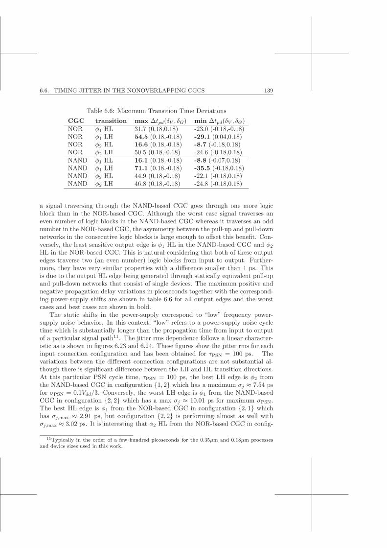
6.6. TIMING JITTER IN THE NONOVERLAPPING CGCS 139
Table 6.6: Maximum Transition Time DeviationsCGC transition max Δtpd(δV , δG) min Δtpd(δV , δG)NOR φ1 HL 31.7 (0.18,0.18) -23.0 (-0.18,-0.18)NOR φ1 LH 54.5 (0.18,-0.18) -29.1 (0.04,0.18)NOR φ2 HL 16.6 (0.18,-0.18) -8.7 (-0.18,0.18)NOR φ2 LH 50.5 (0.18,-0.18) -24.6 (-0.18,0.18)NAND φ1 HL 16.1 (0.18,-0.18) -8.8 (-0.07,0.18)NAND φ1 LH 71.1 (0.18,-0.18) -35.5 (-0.18,0.18)NAND φ2 HL 44.9 (0.18,-0.18) -22.1 (-0.18,0.18)NAND φ2 LH 46.8 (0.18,-0.18) -24.8 (-0.18,0.18)
a signal traversing through the NAND-based CGC goes through one more logicblock than in the NOR-based CGC. Although the worst case signal traverses aneven number of logic blocks in the NAND-based CGC whereas it traverses an oddnumber in the NOR-based CGC, the asymmetry between the pull-up and pull-downnetworks in the consecutive logic blocks is large enough to offset this benefit. Con-versely, the least sensitive output edge is φ1 HL in the NAND-based CGC and φ2
HL in the NOR-based CGC. This is natural considering that both of these outputedges traverse two (an even number) logic blocks from input to output. Further-more, they have very similar properties with a difference smaller than 1 ps. Thisis due to the output HL edge being generated through statically equivalent pull-upand pull-down networks that consist of single devices. The maximum positive andnegative propagation delay variations in picoseconds together with the correspond-ing power-supply shifts are shown in table 6.6 for all output edges and the worstcases and best cases are shown in bold.
The static shifts in the power-supply correspond to “low” frequency power-supply noise behavior. In this context, “low” refers to a power-supply noise cycletime which is substantially longer than the propagation time from input to outputof a particular signal path11. The jitter rms dependence follows a linear character-istic as is shown in figures 6.23 and 6.24. These figures show the jitter rms for eachinput connection configuration and has been obtained for τPSN = 100 ps. Thevariations between the different connection configurations are not substantial al-though there is significant difference between the LH and HL transition directions.At this particular PSN cycle time, τPSN = 100 ps, the best LH edge is φ2 fromthe NAND-based CGC in configuration {1, 2} which has a maximum σj ≈ 7.54 psfor σPSN = 0.1Vdd/3. Conversely, the worst LH edge is φ1 from the NAND-basedCGC in configuration {2, 2} which has a max σj ≈ 10.01 ps for maximum σPSN.The best HL edge is φ1 from the NOR-based CGC in configuration {2, 1} whichhas σj,max ≈ 2.91 ps, but configuration {2, 2} is performing almost as well withσj,max ≈ 3.02 ps. It is interesting that φ2 HL from the NOR-based CGC in config-
11Typically in the order of a few hundred picoseconds for the 0.35μm and 0.18μm processesand device sizes used in this work.

140 CHAPTER 6. JITTER GENERATION IN NONOVERLAPPING CGCS
CGC {1, 1}
σPSN [% of Vdd]
σj
[ps]
CGC {1, 2}
σPSN [% of Vdd]
σj
[ps]
CGC {2, 1}
σPSN [% of Vdd]
σj
[ps]
CGC {2, 2}
σPSN [% of Vdd]
σj
[ps]
NOR φ1 LHNOR φ2 LHNAND φ1 LHNAND φ2 LH
NOR φ1 LHNOR φ2 LHNAND φ1 LHNAND φ2 LH
NOR φ1 LHNOR φ2 LHNAND φ1 LHNAND φ2 LH
NOR φ1 LHNOR φ2 LHNAND φ1 LHNAND φ2 LH
0 0.5 1 1.5 2 2.5 3 3.50 0.5 1 1.5 2 2.5 3 3.5
0 0.5 1 1.5 2 2.5 3 3.50 0.5 1 1.5 2 2.5 3 3.5
0
2
4
6
8
10
0
2
4
6
8
10
0
2
4
6
8
10
0
2
4
6
8
10
Figure 6.23: LH timing jitter standard deviations as function of power-supply noise forτPSN = 100 ps and different CGC connection configurations.
CGC {1, 1}
σPSN [% of Vdd]
σj
[ps]
CGC {1, 2}
σPSN [% of Vdd]
σj
[ps]
CGC {2, 1}
σPSN [% of Vdd]
σj
[ps]
CGC {2, 2}
σPSN [% of Vdd]
σj
[ps]
NOR φ1 HLNOR φ2 HLNAND φ1 HLNAND φ2 HL
NOR φ1 HLNOR φ2 HLNAND φ1 HLNAND φ2 HL
NOR φ1 HLNOR φ2 HLNAND φ1 HLNAND φ2 HL
NOR φ1 HLNOR φ2 HLNAND φ1 HLNAND φ2 HL
0 0.5 1 1.5 2 2.5 3 3.50 0.5 1 1.5 2 2.5 3 3.5
0 0.5 1 1.5 2 2.5 3 3.50 0.5 1 1.5 2 2.5 3 3.5
0
2
4
6
8
10
0
2
4
6
8
10
0
2
4
6
8
10
0
2
4
6
8
10
Figure 6.24: HL timing jitter standard deviations as function of power-supply noise forτPSN = 100 ps and different CGC connection configurations.

6.6. TIMING JITTER IN THE NONOVERLAPPING CGCS 141
1/τPSN [Hz]
σj
[ps]
CGC {1, 1} LH transition
1/τPSN [Hz]
σj
[ps]
CGC {1, 2} LH transition
1/τPSN [Hz]
σj
[ps]
CGC {2, 1} LH transition
1/τPSN [Hz]
σj
[ps]
CGC {2, 2} LH transition
NOR CGC φ1
NOR CGC φ2
NAND CGC φ1
NAND CGC φ2
NOR CGC φ1
NOR CGC φ2
NAND CGC φ1
NAND CGC φ2
NOR CGC φ1
NOR CGC φ2
NAND CGC φ1
NAND CGC φ2
NOR CGC φ1
NOR CGC φ2
NAND CGC φ1
NAND CGC φ2
108 109 1010 1011108 109 1010 1011
108 109 1010 1011108 109 1010 1011
0
2
4
6
8
10
12
0
2
4
6
8
10
12
0
2
4
6
8
10
12
0
2
4
6
8
10
12
Figure 6.25: LH timing jitter rms as function of power-supply noise cycle rate for thedifferent connection configurations.
uration {2, 2} has almost as low jitter, σj,max ≈ 3.52 ps, as the best edge, φ1, whichmeans the symmetry between consecutive pull-up and pull-down networks is quitegood even though no particular attention was made to facilitate this. This alsoshows that in a noisy power-supply environment, a well chosen sampling edge canhave a relative jitter rms of about 0.1% of the clock cycle period whereas a poorlychosen sampling edge can have a jitter rms that is five times higher than this.
The spectral properties of the clock generation circuits are obtained by vary-ing the power-supply noise cycle time, τPSN = {10, 50, 80, 100, 200, 800, 103, 104}ps, between simulation runs. Figures 6.25 and 6.26 show that the clock gener-ation circuits share the low-pass characteristics of their constituent logic blocks.These results have been obtained for the maximum power-supply noise rms value,σPSN = 0.1Vdd/3. For intermediate PSN frequencies, the properties from figures6.23 and 6.24 are displayed. These frequencies correspond to PSN cycle periodssimilar to the constituent logic blocks’ individual propagation delays and a peakingcan be discerned. This peaking occurs due to constructive interference for sig-nals traversing more than one logic block between input and output. In the caseof well matched pull-up and pull-down network strengths, for intermediate PSNfrequencies, the paths with more than one logic block lose the propagation delaycancellation property between consecutive blocks that is valid for lower PSN fre-quencies. The possibility of opposite power-supply polarities between consecutive
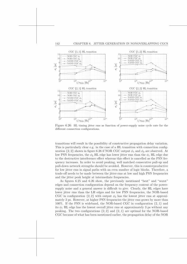
142 CHAPTER 6. JITTER GENERATION IN NONOVERLAPPING CGCS
1/τPSN [Hz]
σj
[ps]
CGC {1, 1} HL transition
1/τPSN [Hz]
σj
[ps]
CGC {1, 2} HL transition
1/τPSN [Hz]
σj
[ps]
CGC {2, 1} HL transition
1/τPSN [Hz]
σj
[ps]
CGC {2, 2} HL transition
NOR CGC φ1
NOR CGC φ2
NAND CGC φ1
NAND CGC φ2
NOR CGC φ1NOR CGC φ2NAND CGC φ1NAND CGC φ2
NOR CGC φ1
NOR CGC φ2
NAND CGC φ1
NAND CGC φ2
NOR CGC φ1
NOR CGC φ2
NAND CGC φ1
NAND CGC φ2
108 109 1010 1011108 109 1010 1011
108 109 1010 1011108 109 1010 1011
0
2
4
6
8
10
12
0
2
4
6
8
10
12
0
2
4
6
8
10
12
0
2
4
6
8
10
12
Figure 6.26: HL timing jitter rms as function of power-supply noise cycle rate for thedifferent connection configurations.
transitions will result in the possibility of constructive propagation delay variation.This is particularly clear e.g. in the case of a HL transition with connection config-uration {2, 2} shown in figure 6.26 if NOR CGC output φ1 and φ2 are observed. Atlow PSN frequencies, the φ2 HL edge has lower jitter rms than the φ1 HL edge dueto the destructive interference effect whereas this effect is cancelled as the PSN fre-quency increases. In order to avoid peaking, well matched consecutive pull-up andpull-down network strengths should be avoided. However, this is counterproductivefor low jitter rms in signal paths with an even number of logic blocks. Therefore, atrade-off needs to be made between the jitter-rms at low and high PSN frequenciesand the jitter peak height at intermediate frequencies.
As figures 6.25 and 6.26 show, the previously mentioned “best” and “worst”edges and connection configuration depend on the frequency content of the power-supply noise and a general answer is difficult to give. Clearly, the HL edges havelower jitter rms than the LH edges and for low PSN frequencies, the NOR-basedCGC in configuration {2, 2} with output φ2 has the lowest jitter rms at approxi-mately 2 ps. However, at higher PSN frequencies the jitter rms grows by more than100%. If the PSN is wideband, the NOR-based CGC in configuration {2, 1} andits φ1 HL edge has the lowest overall jitter rms at approximately 3 ps without anypeaking. The two configurations {2, 2} and {2, 1} are optimal for the NOR-basedCGC because of what has been mentioned earlier, the propagation delay of the NOR

6.7. SUMMARY 143
block is lower if in2 is driven because it is closer to the NOR output. Actually, theconfigurations {2, 2} and {2, 1} are equivalent for φ1 HL, and configurations {1, 2}and {2, 2} are equivalent for φ2 HL.
6.7 Summary
This chapter has presented an investigation of power-supply noise induced timingjitter in two nonoverlapping clock generation circuit architectures. Also, the con-stituent logic blocks were analysed and new mathematical results for the inverterwere given that directly relate the noise on the power and ground lines to the LH andHL jitter rms amounts. The closed-form expressions were thoroughly verified withSPICE simulations and their accuracy was proved. It was determined that the con-stituent logic blocks have a linear relation between the rms power-supply noise andthe rms propagation delay variation (jitter). Two factors are important when pre-dicting the power-supply noise sensitivity of a logic block: (i) overshoot/undershootand (ii) switching speed. The larger the overshoot/undershoot, i.e. the larger theinput capacitance, the more jitter impact because of power-supply noise is obtained.However, the faster the switching speed, the lower the sensitivity of the propagationdelay to power-supply deviations. It was also shown that the jitter rms dependenceon the power-supply noise is very similar for the inverter and NAND and NORblocks.
Furthermore, the logic blocks have a low-pass PSN frequency characteristic.This is because the output voltage slope is primarily dependent on the power-supplydeviation and not the power-supply deviation slope. Therefore, both nonoverlap-ping clock generation circuits have low-pass characteristics. However, they alsodisplay jitter peaking at intermediate frequencies that correspond to the propaga-tion delay of the individual logic blocks. This peaking is not present in all switchingdirection jitter spectra but depends on the signal path within the clock generationcircuit. Generally, the NOR-based CGC in configurations {2, 2} and {2, 1} providesthe least sensitive output edge, φ1 HL, that is optimal for use as a sampling timereference.

Chapter 7Conclusions
Timing uncertainties are an important source of noise in a data conversion system.As signal bandwidths and sampling speeds continue to increase in search of higherdata transfer rates, the effects of timing jitter will grow which means a thoroughunderstanding of the noise injection mechanisms are important in order to devisestrategies to circumvent jitter related problems.
The first part of this thesis has investigated the jitter attributed noise injectionmechanisms in switched-capacitor circuits and translated the results to performanceimpact in switched-capacitor Sigma-Delta modulators. Three effects attributed totiming jitter were identified and described: non-uniform sampling effects, varying-phase-length effects, and phase overlap effects. Closed-form expressions were devel-oped for each of the effects to facilitate easy and accurate jitter impact predictionbased on fundamental circuit parameters. The validity of the predicted jitter im-pact was verified with MATLAB level simulations based on state-space equations.Furthermore, the effects were compared in relevance and it was found that in awideband situation where the sampling switches have been sized properly to al-low for good settling accuracy, the dominant jitter-induced effect is non-uniformsampling.
The second part of this dissertation presented and analysed two new sampling cir-cuit topologies with reduced sensitivity to timing uncertainties: the parallel samplerand the Sigma-Delta sampler. Both are based on the understanding of what param-eters influence the non-uniform sampling noise power. The parallel sampler obtainsa reduced jitter sensitivity based on averaging between multiple clock signals whichsets an independency requirement on the time references whereas the Sigma-Deltasampler pushes the jitter-induced noise away from the signal band through noiseshaping.
A method of meeting the independency requirement while solving the problem ofmultiple clock generation for the parallel sampler was also presented in the form of
145
146 CHAPTER 7. CONCLUSIONS
delay line based clock generation. This clock generation method uses the propertythat the correlation between jitter of different clock cycles decreases as the numberof cycles between them increases. The delay line was thoroughly described andanalysed from quality viewpoints such as delay jitter and static delay errors. Itwas found that the delay line quality is a dominant factor in the jitter suppressionperformance of the parallel sampler and as the length of the delay line grows, thenoise spectrum becomes more colored with power accumulating around the signalfrequency even though the full band suppression remains unchanged compared withthe ideal case. Also, it was shown that the kBT/C noise of the parallel sampler isnot worse than the noise for an ordinary sampler which might be the initial guessdue to the use of small capacitors. Moreover, it was shown that the capacitormismatch effects are very small and only give rise to a gain deviation in the non-uniform sampling noise power of about 0.2%. Finally, all performance predictionsobtained in the form of mathematical relations were verified with simulations inMATLAB using the state-space equation approach.
The jitter suppression performance of the Sigma-Delta sampler depends on thespectral composition of the signal and is improved compared to a standard samplingcircuit if the mass center of the signal spectrum is higher than the midpoint of thesignal band. The SJNR of the Sigma-Delta sampler is virtually independent ofthe signal frequency which is very different from a standard sampler which hasan inverse square relationship. This means that the Sigma-Delta sampler is moresuitable for operating at higher signal frequencies and lower oversampling ratiosas the non-uniform sampling impact is far less than for an ordinary sampler. Theoperation and theoretical performance of the Sigma-Delta sampler were describedand verified with MATLAB level simulations. Furthermore, mismatch effects wereanalysed and simulated showing them to be insignificant.
The third part of this thesis has looked into the timing uncertainty generation pro-cess from the power-supply noise and substrate noise perspective in two nonover-lapping clock generation circuits. The analysed clock generation circuits were disas-sembled into their constituent parts and each part was described separately. Closed-form expressions for the jitter dependence on power-supply variations were obtainedfor the inverter block and the results were verified with BSIM3v3 transistor levelSPICE simulations. Two CMOS processes were used for verification purposes:0.35μm and 0.18μm. For the 0.35μm process, model parameters were fitted in-cluding nonlinear and time-varying parasitic capacitors of both PMOS and NMOSdevices and it was shown that the closed-form transient expressions show a highlevel of accuracy. The 0.18μm process was used as a reference for the closed-form ex-pressions to demonstrate that the linear relations extend into smaller feature sizes.The more complicated circuit blocks and the whole clock generation circuits werecharacterized through SPICE simulations and their behaviors and performanceswere explained on a system level.
It was determined that the two investigated nonoverlapping clock generation

147
circuits have no major differences in power-supply noise sensitivity if they are ofsimilar size and if similar signal paths are considered. However, for best performanceand lowest jitter injection it is crucial that each constituent component’s speed ismaximized. Furthermore, even though the clock generation circuits have a low-passshaped jitter spectrum, the possibility of peaks in this spectrum was discovered.The peaks are due to constructive delay interference in the clock generation circuitcomponents. To minimize the peaking, the various component delays should bedesigned to have significant differences and if cyclic behavior in the power-supplynoise is expected, propagation delays which are multiples of the power-supply noisecycles should be avoided. However, this design strategy will not only lower thepeak but it will also raise the jitter rms for other PSN frequencies which is why atrade-off has to be made between jitter peak height and average level.


Appendix ATheoretical ADC Efficiency Limit
Naturally, an analog signal must be transferred both into time-discrete and amplitude-discrete domains in the digitization process. The first part is called sampling andtypically involves storing the analog voltage on a capacitor which, at some point intime, is then disconnected from the analog voltage. What is sampled is not onlythe analog voltage but also noise that is always present. Restricting this deductionto thermal noise, the spectral density of the squared noise voltage is of the formV 2
n = 4kBTR, where kB = 1.38 · 10−23 [J/K] is Boltzmann’s constant, T is theabsolute temperature, and R is the resistance of the noise generating element (e.g.a transistor switch) [42]. Connecting a switch to a capacitor in a configurationshown in the sampling structure from figure 1.5 results in noise filtering since aseries resistor followed by a shunt capacitor represents a low-pass filter (see fig.A.1). The voltage transfer function in frequency-domain of such a filter is simpleto deduce by using Ohm’s law and the definition of capacitance, C = Q/V . Twoways of expressing the current in the filter are obtained1.
i =vn − vnC
R= C
dvnC
dt(A.1)
vn
C
R
i
vnC
Figure A.1: A simple RC filter used to demonstrate the origin of kBT/C noise.
1Note that a lower case variable, e.g. vn, refers to time-domain while the uppercase version,i.e. Vn, corresponds to the variable in frequency-domain.
149
150 APPENDIX A. THEORETICAL ADC EFFICIENCY LIMIT
Taking the Fourier transform and noting that F{dx/dt} = jωX, the transfer func-tion is simply
H =VnC
Vn=
11 + jωRC
(A.2)
where ω = 2πf . The total squared voltage on the capacitor is, because of Parseval’sformula
v2nC = 4kBTR
∫ ∞
0
H2df = 4kBTR
∫ ∞
0
11 + (ωRC)2
=4kBTR
4RC=kBT
C(A.3)
If this capacitor is charged and discharged with frequency fs, the maximum sam-pling power consumption becomes
P = CV 2reffs (A.4)
As shown in chapter 2, the quantization noise power of an ideal ADC is q2RMS =V 2
LSB/12. If the ADC is to be dominated by quantization noise and not thermalnoise, a constraint would be to limit the thermal noise to degrade the SQNR bymaximum 1 dB [24]. This means that the thermal noise can add a maximum of1 dB to the quantization noise power which translates to 101/10 ≈ 1.25, i.e. thethermal noise is max 25% of the quantization noise. Hence,
kBT
C<
V 2ref
22n · 12 · 4 ⇒ V 2refC > 48kBT22n (A.5)
so P > 48kBT22nfs which represents a lower bound for an ADC power consumptionwhere the quantization noise power should dominate over thermal noise. Naturally,this measure is very limited because only thermal noise is taken into account andalso only power consumption during sampling is taken into account, i.e. activecircuitry efficiency is infinite [80]. However, from this deduction comes a commonlyused figure of merit, called conversion energy or quantization energy (cf eq. (2.9)),that indicates how efficient an ADC is
E =P
2nfs> 48kBT2n [J/conversion] (A.6)

Bibliography
[1] William Shockley. “Patent 2,569,347, Circuit Element Utilizing SemiconductiveMaterial”. United States Patent Office, September 1951. Patent applied forJune 26, 1948.
[2] Robert Noyce. “Patent 2,981,877, Semiconductor Device-and-Lead Structure”.United States Patent Office, April 1961. Patent applied for July 30, 1959.
[3] Jack Kilby. “Patent 3,138,743, Miniaturized Electronic Circuits”. United StatesPatent Office, June 1964. Patent applied for February 6, 1959.
[4] Gordon E. Moore. “Cramming more components onto integrated circuits”.Electronics magazine, volume 38, no. 8, pp. 114–117, April 1965.
[5] Radhakrishna Hiremane. “From Moore’s Law to Intel Innovation – Predictionto Reality”. Technology @ Intel Magazine, pp. 1–9, April 2005.
[6] Gordon E. Moore. “Progress in digital integrated electronics”. Proceedings ofthe International Electron Devices Meeting, volume 21, pp. 11–13, 1975.
[7] “Microprocessor Quick Reference Guide”. Intel website. http://www.intel.com/pressroom/kits/quickref.htm.
[8] Frank M. Wanlass. “Patent 3,356,858, Low Standby-Power ComplementaryField Effect Circuitry”. United States Patent Office, December 1967. Patentapplied for June 18, 1963.
[9] Ram Krishnamurthy. “DSP Circuit Technologies for the Nano-scale Era”. In-vited speaker: Swedish System-on-Chip Conference, May 2006.
[10] Mikael Östling et. al. “High Frequency Silicon – Background”. http://www.imit.kth.se/info/FOFU/hfsilicon/chapter2.htm. KTH - Royal Instituteof Technology.
[11] Walt Kester, Dan Sheingold, James Bryant, Walt Jung, et. al. Analog-DigitalConversion. Analog Devices, Inc., 2004. ISBN: 0-916550-27-3.
[12] K. W. Cattermole. Principles of pulse code modulation. ILiffe Books Ltd.,London, 1969. ISBN: 592-02834-8.
151

152 BIBLIOGRAPHY
[13] Paul M. Rainey. “Patent 1,608,527, Facsimile Telegraph System”. United StatesPatent Office, November 1926. Patent applied for July 20, 1921.
[14] Alec Harley Reeves. “Patent 2,272,070, Electric Signaling System”. UnitedStates Patent Office, February 1942. Patent applied for November 22, 1939.Also French Patent 852183 issued 1938, and British Patent 538860 issued 1939.
[15] Alan V. Oppenheim, Alan S. Willsky, and S. Hamid Nawab. Signals & Systems.Prentice-Hall International, Inc., 1997. ISBN: 0-13-651175-9.
[16] Harold S. Black and J.O. Edson. “Pulse Code Modulation”. AIEE Transac-tions, volume 66, pp. 895–899, 1947.
[17] Harold S. Black. “Pulse Code Modulation”. Bell Labs Record, volume 25, pp.265–269, July 1947.
[18] William M. Goodall. “Telephony by Pulse Code Modulation”. Bell SystemTechnical Journal, volume 26, pp. 395–409, July 1947.
[19] Edmond Maurice Deloraine, Stanislas Van Mierlo, and Boris Derjavitch.“Patent 2,629,857, Communication System Utilizing Constant AmplitudePulses of Opposite Polarities”. United States Patent Office, February 1953.Patent applied for October 8, 1947. Also French patent 932,140 issued August1946, and British patent 627,262 issued 1949.
[20] Steven R. Norsworthy, Richard Schreier, and Gabor C. Temes, eds. Delta-Sigma Data Converters - Theory, Design, and Simulation. IEEE Press, 1997.
[21] Cassius C. Cutler. “Patent 2,927,962, Transmission Systems Employing Quan-tization”. United States Patent Office, March 1960. Patent applied for April26, 1954.
[22] Toshio Hayashi, Yasunobu Inabe, Kuniharu Uchimura, and Atsushi Iwata. “AMultistage Delta-Sigma Modulator without Double Integration Loop”. ISSCCDigest of Technical Papers, pp. 182–183, February 1986.
[23] L. Richard Carley. “A Noise-Shaping Coder Topology for 15+ bit Converters”.IEEE Journal of Solid-State Circuits, volume SC-24, pp. 267–273, April 1989.
[24] Kent H. Lundberg. “High-Speed Analog-to-Digital Converter Survey”. In-ternet, October 2002. Department of Electrical Engineering and ComputerScience, MIT, http://web.mit.edu/klund/www/papers/UNP−flash.pdf.
[25] Yuan Taur and Tak H. Ning. Fundamentals of Modern VLSI Devices. Cam-bridge University Press, 1998. ISBN: 0-521-55959-6.
[26] Jan M. Rabaey, Anantha Chandrakasan, and Borivoje Nikolic. Digital Inte-grated Circuits - A Design Perspective. Pearson Education International, 2nd
edition edition, 2003. ISBN: 0-13-120764-4.
153
[27] Ali Hajimiri and Thomas H. Lee. Low Noise Oscillators. Kluwer AcademicPublishers, 1999. ISBN: 0-7923-8455-5.
[28] “Online Etymological Dictionary”. Internet, 2001. http://www.etymonline.com.
[29] Lennart Råde and Bertil Westergren. Mathematics Handbook for Science andEngineering. Studentlitteratur, 3rd edition, 1995. ISBN: 91-44-25053-3.
[30] Leon Cohen. “The Generalization of the Wiener-Khinchin Theorem”. Proceed-ings of the IEEE International Conference on Acoustics, Speech, and SignalProcessing, volume 3, pp. 1577–1580, May 1998.
[31] John A. McNeill. “Jitter in Ring Oscillators”. IEEE Journal of Solid-StateCircuits, volume 32, no. 6, pp. 870–879, June 1997.
[32] Golledge Electronics Ltd. “Product datasheet GTXO-92 and HCD666”. Inter-net. http://www.golledge.com.
[33] Thomas H. Lee and Ali Hajimiri. “Oscillator Phase Noise: A Tutorial”. IEEEJournal of Solid-State Circuits, volume 35, no. 3, pp. 326–336, March 2000.
[34] Behzad Razavi. RF Microelectronics. Prentice-Hall Inc., 1998. ISBN: 0-13-887571-5.
[35] Ana Rusu and Mohammed Ismail. “Sigma-Delta Design Solutions for 4G Wire-less”. KTH - RaMSiS Summer School, July 2006.
[36] Murray R. Spiegel. Schaum’s Mathematical Handbook of Formulas and Tables.McGraw-Hill, 1968.
[37] Kai Chang. RF and Microwave Wireless Systems. John Wiley & Sons, Inc.,2000. ISBN: 0-471-35199-7.
[38] Tomi Engdahl. “Cable Impedance”. Internet, May 2004. http://www.epanorama.net/documents/wiring/cable−impedance.html.
[39] Wai-Kai Chen. The VLSI Handbook. CRC Press LLC, 2004.
[40] Roger L. Freeman. Fundamentals of Telecommunications. John Wiley & Sons,Inc., 1999.
[41] Kent H. Lundberg. “Analog-to-Digital Converter Testing”. Internet, Octo-ber 2002. Department of Electrical Engineering and Computer Science, MIT,http://web.mit.edu/klund/www/papers/UNP−A2Dtest.pdf.
[42] David Johns and Ken Martin. Analog Integrated Circuit Design. John Wiley& Sons, Inc., 1997. ISBN: 0-471-14448-7.
154 BIBLIOGRAPHY
[43] Vaughan Wesson. “TN200410A - Dynamic Range”. Internet, October 2004.http://www.seis.com.au/TechNotes/TN200410A−SNR.html.
[44] IEEE Std 1241-2000. “IEEE Standard for Terminology and Test Methods forAnalog-to-Digital Converters”, December 2000.
[45] Maxim Integrated Products. “Application Note 1023: UnderstandingPipelined ADCs”. Internet, March 2001. http://www.maxim-ic.com/an1023.
[46] Jaana Riikonen, Mikko Aho, Väinö Hakkarainen, Kari Halonen, and LauriSumanen. “A 10-bit 400-MS/s 170mW 4-Times Interleaved A/D Converterin 0.35-μm BiCMOS”. Proceedings of the IEEE International Symposium onCircuits and Systems, volume 5, pp. 4622–4625, May 2005.
[47] Jesper Steensgaard-Madsen. “High-Performance Data Converters”. Ph.D. the-sis, The Technical University of Denmark, Lyngby, Denmark, 1999.
[48] William R. Bennett. “Spectra of Quantized Signals”. Bell System TechnicalJournal, volume 27, pp. 446–472, July 1948. The current name of the journalis Bell Labs Technical Journal.
[49] Bernard Widrow. “A Study of Rough Amplitude Quantization by means ofNyquist Sampling Theory”. IRE Transactions on Circuit Theory, volume CT-3, pp. 266–276, December 1956.
[50] Anekal B. Sripad and Donald L. Snyder. “A Necessary and Sufficient Condi-tion for Quantization Errors to be Uniform and White”. IEEE Transactionson Acoustis, Speech and Signal Processing, volume ASSP-25, pp. 442–448, Oc-tober 1977.
[51] Thomas E. Parker. “Characteristics and Sources of Phase Noise in StableOscillators”. Proceedings of the 41st Annual Frequency Control Symposium,pp. 99–110, 1987.
[52] Steve Williamson. “How To Design RF Circuits - Synthesisers”. IEE TrainingCourse - How to Design RF Circuits, pp. 8/1 – 8/11, April 2000.
[53] Hai Tao, László Tóth, and John M. Khoury. “Analysis of Timing Jitter inBandpass Sigma-Delta Modulators”. IEEE Transactions on Circuits and Sys-tems – II: Analog and Digital Signal Processing, volume 46, no. 8, pp. 991–1001,August 1999.
[54] Haruo Kobayashi, Masanao Morimura, Kensuke Kobayashi, and YoshitakaOnaya. “Aperture Jitter Effects in Wideband ADC Systems”. Proceedings ofthe 38th Annual Society of Instrument and Control Engineers Conference, pp.1089–1094, July 1999.
155
[55] Kuniharu Uchimura, Toshio Hayashi, Tadakatsu Kimura, and Atsushi Iwata.“Oversampling A-to-D and D-to-A Converters with Multistage Noise ShapingModulators”. IEEE Transactions on Acoustics, Speech, and Signal Processing,volume 36, no. 12, pp. 1899–1905, December 1988.
[56] Ahmed Gharbiya and David A. Johns. “On The Implementation of Input-Feedforward Delta-Sigma Modulators”. IEEE Transactions on Circuits andSystems – II: Express Briefs, volume 53, no. 6, pp. 453–457, June 2006.
[57] Mark N. Horenstein. Microelectronic Circuits and Devices. Prentice Hall,1996.
[58] Bengt Jonsson, Svante Signell, Helge Stenström, and Nianxiong Tan. “Dis-tortion in sampling”. Proceedings of the IEEE International Symposium onCircuits and Systems, pp. 445–448, June 1997.
[59] Frank Herzel, Gunter Fischer, Hans Gustat, and Peter Weger. “An IntegratedCMOS PLL for Low-Jitter Applications”. IEEE Transactions on Circuits andSystems –II: Analog and Digital Signal Processing, volume 49, no. 6, pp. 427–429, June 2002.
[60] Gang Yan, Chenxiao Ren, Zhendong Guo, Qing Ouyang, and ZhongyuanChang. “A Self-Biased PLL With Current-Mode Filter For Clock Genera-tion”. Proceedings of the IEEE International Solid-State Circuits Conference,volume 1, pp. 420–421, February 2005.
[61] Stephen Williams, Hugh Thompson, Michael Hufford, and Eric Naviasky. “AnImproved CMOS Ring Oscillator PLL with Less than 4ps RMS AccumulatedJitter”. Proceedings of the IEEE Custom Integrated Circuits Conference, pp.151–154, October 2004.
[62] Nicola Da Dalt, Moritz Harteneck, Christoph Sandner, and Andreas Wies-bauer. “On the Jitter Requirements of the Sampling Clock for Analog-to-Digital Converters”. IEEE Transactions on Circuits and Systems – I: Funda-mental Theory and Applications, volume 49, no. 9, pp. 1354–1360, September2002.
[63] Alan Hastings. The Art of Analog Layout. Pearson Education Inc., 2001.
[64] Athanasios Papoulis and S. Unnikrishna Pillai. Probability, Random Variablesand Stochastic Processes. McGraw-Hill, 4 edition, 2002.
[65] Saska Lindfors, Aarno Pärssinen, and Kari A. I. Halonen. “A 3-V 230-MHzCMOS Decimation Subsampler”. IEEE Transactions on Circuits and Systems– II: Analog and Digital Signal Processing, volume 50, no. 3, pp. 105–117,March 2003.
156 BIBLIOGRAPHY
[66] Peter Händel, Ragnar Ottoson, and Håkan Hjalmarsson. “Signalteori 2000”.KTH - Royal Institute of Technology, January 2000. Course compendium.
[67] John G. Maneatis. “Low-Jitter Process-Independent DLL and PLL Based onSelf-Biased Techniques”. IEEE Journal of Solid-State Circuits, volume 31,no. 11, pp. 1723–1732, November 1996.
[68] William J. Dally and John W. Poulton. Digital Systems Engineering. Cam-bridge University Press, 1998. ISBN: 0-521-59292-5.
[69] Paul R. Gray, Paul J. Hurst, Stephen H. Lewis, and Robert G. Meyer. Analysisand Design of Analog Integrated Circuits. John Wiley & Sons, 4th editionedition, 2001. ISBN: 0-471-32168-0.
[70] Teppo Karema. “Oversampling A/D and D/A Converters Using One-BitSigma-Delta Modulation Techniques”. Ph.D. thesis, Tampere University ofTechnology, Tampere FIN-33101, Finland, August 1994.
[71] Maurits Ortmanns, Friedel Gerfers, and Yiannos Manoli. “Clock Jitter Insensi-tive Continuous-Time ΣΔ Modulators”. Proceedings of the IEEE InternationalConference on Electronics, Circuits and Systems, volume 2, pp. 1049–1052,September 2001.
[72] ———. “A Continuous-Time ΣΔ Modulator With Reduced Sensitivity toClock Jitter Through SCR Feedback”. IEEE Transactions on Circuits andSystems – I: Regular Papers, volume 52, no. 5, pp. 875–884, May 2005.
[73] Adam Strak. “Analysis of Clock Jitter Effects in Wideband Sigma Delta Con-verters for RF-Applications”. Master’s thesis, KTH - Royal Institute of Tech-nology, Dept. of Microelectronics and Information Technology, May 2002.
[74] David C. Lee. “Analysis of Jitter in Phase-Locked Loops”. IEEE Transactionson Circuits and Systems – II: Analog and Digital Signal Processing, volume 49,no. 11, pp. 704–711, November 2002.
[75] Ken Martin and Adel S. Sedra. “Switched-Capacitor Building Blocks for Adap-tive Systems”. IEEE Transactions on Acoustics, Speech, and Signal Processing,volume ASSP-29, no. 3, pp. 736–744, June 1981.
[76] Stephen H. Lewis. “Video-Rate Analog-to-Digital Conversion Using PipelinedArchitectures”. Memorandum UCB/ERL M87/90, Electronics Research Lab-oratory, U.C. Berkeley, November 1987. Pp. 96–98.
[77] David A. Hodges, Horace G. Jackson, and Resve A. Saleh. Analysis and Designof Digital Integrated Circuits. McGraw Hill, 3rd edition, 2003.
157
[78] Takayasu Sakurai and A. Richard Newton. “Alpha-Power Law MOSFETModel and its Applications to CMOS Inverter Delay and Other Formulas”.IEEE Journal of Solid State Circuits, volume 25, no. 2, pp. 584–594, April1990.
[79] Frank Herzel and Behzad Razavi. “A Study of Oscillator Jitter Due to Supplyand Substrate Noise”. IEEE Transactions on Circuits and Systems – II: Analogand Digital Signal Processing., volume 46, no. 1, pp. 56–62, January 1999.
[80] Eric A. Vittoz. “Future of Analog in the VLSI Environment”. IEEE Inter-national Symposium on Circuits and Systems, volume 2, pp. 1372–1375, May1990.