thwarting security threats from malicious fpga tools with ... · this article has been accepted for...
TRANSCRIPT

This article has been accepted for inclusion in a future issue of this journal. Content is final as presented, with the exception of pagination.
IEEE TRANSACTIONS ON VERY LARGE SCALE INTEGRATION (VLSI) SYSTEMS 1
Thwarting Security Threats From Malicious FPGATools With Novel FPGA-Oriented
Moving Target DefenseZhiming Zhang, Laurent Njilla, Member, IEEE, Charles A. Kamhoua, Senior Member, IEEE,
and Qiaoyan Yu , Senior Member, IEEE
Abstract— The increasing usage and popularity of thefield-programmable gate array (FPGA) systems bring in securityconcerns. Existing countermeasures are mostly based on theassumption that the computer-aided design (CAD) tools forFPGA configuration are trusted. Unfortunately, this assump-tion does not always hold. In this paper, we investigate thepotential security threats originated from the untrusted CADtools. Furthermore, we exploit the principle of moving targetdefense (MTD) to propose an FPGA-oriented MTD (FOMTD)method. The three defense lines in the FOMTD generate uncer-tainties, from the attacker’s point of view, to thwart hardwareTrojan insertion attacks. The theoretical upper bound of thehardware Trojan hit rate for each defense line is provided inthis paper. Experimental results show that the proposed defenseline 2 and defense line 3 reduce the Trojan hit rate by up to40% and 91%, respectively, for the scenario where the maliciousCAD tool can insert Trojans in the occupied FPGA slices. Theproposed gate replacement technique in the defense line 3 furtherimproves the attack resilience and obtains 88% reduction on theTrojan hit rate. Compared to the static redundancy-based Trojandetection method, the proposed method achieves better resilienceagainst Trojan insertions and consumes 50% less dynamic power.
Index Terms— Altera, field-programmable gate array (FPGA),FPGA design suite, hardware security, hardware Trojan, movingtarget defense (MTD), Xilinx.
I. INTRODUCTION
F IELD-PROGRAMMABLE gate arrays (FPGAs) enter arapid growth era due to their attractive flexibility and
CMOS-compatible fabrication process. Global Market Insightspredicts that the FPGA market size is expected to reach9.98 billion U.S. dollars by the year 2022 [1]. The increasingpopularity of FPGA may drive more attackers to compromiseFPGA-based systems through various channels. The work [2]
Manuscript received April 7, 2018; revised August 7, 2018 andSeptember 14, 2018; accepted October 16, 2018. This work was sup-ported in part by the National Science Foundation CAREER Award underGrant 1652474 and in part by the Air Force Research Laboratory VisitingFaculty Research Program 2017. DISTRIBUTION A. Approved for publicrelease: distribution unlimited. Case Number: 88ABW-2018-2036. Dated 11May, 2018. (Corresponding author: Qiaoyan Yu.)
Z. Zhang and Q. Yu are with the Department of Electrical and ComputerEngineering, University of New Hampshire, Durham, NH 03824 USA (e-mail:[email protected]).
L. Njilla is with the Cyber Assurance Branch of Air Force ResearchLaboratory, Rome, NY 13441 USA (e-mail: [email protected]).
C. A. Kamhoua is with the Network Security Branch of Army Research Lab-oratory, Adelphi, MD 20783 USA (e-mail: [email protected]).
Color versions of one or more of the figures in this paper are availableonline at http://ieeexplore.ieee.org.
Digital Object Identifier 10.1109/TVLSI.2018.2879878
highlights that the FPGA security embraces four aspects:1) secure operations conducted by FPGA devices; 2) utiliza-tion of FPGAs for system security enhancement; 3) securebitstream delivery to FPGA devices; and 4) exploitation ofFPGA devices as an attack surface to breach FPGA-basedsystems. The aspects 1 and 2 emphasize that the programmablefeatures of FPGAs have been exploited to address the securitychallenges that application-specific integrated circuits (ASICs)are facing. For example, the embedded FPGA is used toperform locking key authentication [3], [4]. However, FPGAshave their own security vulnerabilities. The studies [3], [5]–[8]extensively discuss the aspects 3 and 4.
For the reason of efficiency and economy, the supply chainof modern FPGAs is getting globalized. This trend potentiallyincreases the chance that the FPGA devices or FPGA designtools are not trustworthy. Intellectual property (IP) stealingand tampering could happen in different data formats, such ashardware description language (HDL) and bitstream [3], [12].The integrity of FPGA systems may be harmed by the hard-ware Trojans induced in some stages of the FPGA designflow [9]–[11].
This paper aims to address the Trojan insertion threat frommalicious FPGA computer-aided design (CAD) tools. Morespecifically, we make the following contributions in this paper.
1) We use two practical examples to demonstrate that ahardware Trojan can be injected during several stagesof the FPGA design flow without disturbing the originalHDL design file.
2) We exploit the principle of moving target defense (MTD)and propose an FPGA-Oriented MTD (FOMTD) coun-termeasure to resist the attacks from malicious FPGAtools. To the best of our knowledge, together withour preliminary work [10], [12], our research is thefirst effort that assesses the feasibility of applying theMTD concept to defeat hardware Trojan insertion viamalicious FPGA software.
3) We propose three defense lines to generate three typesof unpredictability, which facilitate to thwart the stealthydesign modification induced by the compromised FPGAsoftware. The first defense line utilizes a user constraintsfile to designate a portion of the design to specific FPGAslices. The second defense line randomly selects one ofthe design replicas at runtime and uses an input gatingtechnique to mute the unused replicas for power saving.The third defense line divides a design into multiple
1063-8210 © 2018 IEEE. Personal use is permitted, but republication/redistribution requires IEEE permission.See http://www.ieee.org/publications_standards/publications/rights/index.html for more information.

This article has been accepted for inclusion in a future issue of this journal. Content is final as presented, with the exception of pagination.
2 IEEE TRANSACTIONS ON VERY LARGE SCALE INTEGRATION (VLSI) SYSTEMS
submodules and assembles the complete design withhot-swappable submodules at runtime, increasing thenumber of design configurations on the FPGA device.
4) We analyze the theoretical upper bound of hardwareTrojan hit rate for each defense line and validate theanalysis through FPGA emulation.
The remainder of this paper is organized as follows.Section II discusses the related work. Section III describesthe attack model used in this paper. Practical attack exampleson two commercial FPGA design suites are provided inSection IV. The FOMTD method is presented in Section V.The theoretical security strength achieved by the three defenselines in the FOMTD method is analyzed in Section V, as well.Extensive evaluation of our method and relevant work is con-ducted in Section VI. We conclude this paper in Section VII.
II. RELATED WORK
One category of existing countermeasures against securitythreats on FPGA systems focuses on IP theft issues duringthe FPGA deployment phase. To avoid information leak-ing through hardware Trojans, the MORPH architecture [13]combines multiple levels of protection schemes, includingmorph operation, onion encryption, replication, partial runtimereconfiguration, and hardware abstraction layer to mitigate theTrojans induced in fabrication time or design time. No hard-ware cost and detailed assessment are available in [13]. In thework [6], a bitstream encryption method is implemented forthe Xilinx Virtex FPGA family. The security protocol forthat encryption scheme protects the IP from being illegallycopied via restricting the access to the configuration file andkey bits. The method in [14] manipulates a state transitiongraph to create a rare property and form watermarks. In thePUF-FSM binding protection mechanism [15], the FSM in anIP can only be activated by the correct response from the PUFembedded in the FPGA. The MUTARCH approach in [16]assigns each FPGA device a unique architecture to encryptthe bitstream distinctively. Only the authorized device canrecognize the encrypted bitstream. However, those bitstreamprotection methods only secure the FPGA implementationduring the bitstream generation stage. Without considering thepotential threats from the mapping and place and route (PAR)stages in the FPGA design flow, FPGA deployment is stillvulnerable to the threats from untrusted FPGA design suite.
Another category of defense efforts is to thwart the secu-rity threats originated from the malicious FPGA devices.The work [17] detects anomalies in the physical layer ofthe FPGA by identifying the basic building block on theFPGA die that has different physical statistical characteristicswith neighboring blocks. In [18], a specific taxonomy ofFPGA-based hardware Trojan attacks is illustrated. That workalso presents an adapted triple modular redundancy (ATMR)to detect hardware Trojans on the FPGAs. The ATMR methodreplicates the design three times, and the third replica isactivated only when the mismatch is found between the firsttwo. In the work [19], the normalized parameters (e.g., powerconsumption and timing variation) are weighted and combinedas a threat detectability metric, which is compared with a
threshold to determine whether a hardware Trojan exists inthe design. The work [20] fills up the unoccupied FPGA spacewith low-level dummy logics to eliminate the FPGA resourceavailable for hardware Trojan insertion. Those methods couldbe nullified if the Trojans are inserted during the process ofFPGA configuration.
There are limited works addressing the attacks from CADtools for FPGAs. Logic testing and side-channel analysis havebeen exploited to detect the hardware Trojans inserted throughthe malicious FPGA design suites [21]. The Multiple Exci-tation of Rare Occurrence (MERO) method [22] provides acompact way to generate test patterns for Trojan detection. Thework [23] leverages the dependence between dynamic currentand maximum operating frequency to detect the hardwareTrojan on FPGAs. Our preliminary work [12] addresses thesecurity challenges occurred during the FPGA deployment forlegacy systems. We apply the pin grounding scheme to theunused FPGA I/O pins to block the communication betweenFPGA Trojans and off-chip world and further propose ahardware MTD to thwart the Trojan insertion by the maliciousCAD tools. We expand our work for legacy systems to generalFPGA applications in [10].
According to the above-mentioned discussions, we con-clude that most of the existing solutions aim for theFPGA security threats either from supply chain or FPGAdevices, not from malicious FPGA design suites. Althoughthe FPGA vendors [24] adopt bit encryption, authentication,and key/register zeroization techniques to prevent bitstreamsfrom being tampered, those methods do not thwart the designmodification before the bitstream is generated by the FPGAsoftware. Our previous works [10], [12] exploit the principleof MTD to generate uncertainty from the attacker’s point ofview, effectively mitigating the hardware Trojans and, thus,protecting the bitstream from being maliciously modified.In this paper, we add theoretical analyses for our countermea-sures, improve the MTD defense strength, and perform moreextensive performance and overhead assessments.
III. ATTACK MODEL
A. Attacks From Malicious FPGA Design Suites
FPGA design software has been considered as poten-tial hardware threats challenging the FPGA security [25].Untrusted FPGA CAD tools can be exploited by the attackersto insert hardware Trojans [26], [27]. As shown in Fig. 1(a),our attack model assumes that the FPGA deployment engi-neers, in-house designs, the bitstream downloading channel,and procedure are trusted. The untrusted phase interested inthis paper is the FPGA configuration, especially the designmapping, PAR stages. The attacks are originated from mali-cious software mounted on top of the original FPGA designsuite for SRAM FPGAs, as shown in Fig. 1(b). The FPGAdesign suite may not be malicious initially, but advancedattackers could exploit the vulnerability of the FPGA designsuite to implant malicious software to the original suitethrough software upgrading. We argue that the FPGA designsuite will be propagated through computer network or retailers,so the integrity of the software may be sabotaged by advanced

This article has been accepted for inclusion in a future issue of this journal. Content is final as presented, with the exception of pagination.
ZHANG et al.: THWARTING SECURITY THREATS FROM MALICIOUS FPGA TOOLS WITH NOVEL FOMTD 3
Fig. 1. Contaminated FPGA design suite leading to a stealthy modificationon the placelist for an FPGA device. (a) Software compromising stage.(b) Malicious software add-on in the supply chain of FPGA tools.
attackers. One motivation example for this type of attackscould be: if an attacker knows the military or bank is about topurchase an FPGA to perform some specific functions. Thesource of FPGA devices and the functional modules (in aformat of HDL) are trusted after the rigorous examination.A stealthy way to compromise the system is through acompromised FPGA design suite.
B. Three Levels of Attacks
As the malicious program is mounted on top of the originalFPGA CAD tool before the FPGA users utilize the FPGAtool and development board, it is reasonable to assume thatthe attacker does not know what exact design will be mappedto the FPGA die. Depending on the attacker’s capability,we classify the attacks into three levels.
1) L-1 Attack: Based on his/her experience, the attackerplaces hardware Trojans in the most popular FPGAdie area. At this level, the attacker does not have anyknowledge of the design to be configured on the FPGA.
2) L-2 Attack: The attacker is capable of extracting infor-mation, such as which FPGA slices are utilized by thecurrent design from the FPGA placelist (i.e., the outputafter placement and routing). Although the attack at thislevel does not analyze the exact function of the design,the exploration space of L-2 attacks is significantlysmaller than that of the L-1 attacks.
3) L-3 Attack: The malicious FPGA CAD tool searches forthe design replicas used by duplication-based defensetechniques and inserts the identical Trojans to eachreplica. Attacks at this level are powerful, as the L-3
Fig. 2. Attack surfaces on the Xilinx FPGA design flow. The rectanglesrepresent the output file from each step. The file with the symbol * is anoutput file modified by the malicious FPGA software.
attacks are able to nullify the countermeasure that simplyduplicates the design. In spite of being the most chal-lenging, L-3 attacks will cost attackers more resourcesto guarantee the success of Trojan insertion attacks.
To make an effective impact on the design function, hard-ware Trojans interested in this paper are the ones alteringthe lookup table (LUT) configuration for the original design.A hardware Trojan is composed of a trigger and a payload.In our attack model, the trigger circuit can be located in eitherthe occupied or unoccupied FPGA slices, but the payloadcircuit must interact with the FPGA area occupied by theoriginal design.
IV. DEMONSTRATION OF ATTACKS FROM MALICIOUS
FPGA SOFTWARE
In this section, we demonstrate two practical attacks throughtwo commercial FPGA design suites. The design suite’sbuilt-in tools are exploited to manually disturb the placelist.
A. Attacks on Xilinx ISE
Fig. 2 depicts the design flow for a Xilinx FPGA designsuite. There are three potential attack surfaces for maliciouslyimplanted FPGA tools to land on. We use Xilinx ISE 14.1 asan example in the following discussion. In the step of mapping,an attacker could introduce additional I/O pins, exchange theexisting I/O pin connection, and modify the slew rate and thevoltage level of I/O pins. As the tampered mapping output_map.ncd* is not readable (unless the FPGA design suiteprovides a program, such as ncd2xdl, to readback the nativecircuit description file), it is not easy to notice the modificationperformed by the malicious FPGA software. More tamperingon the FPGA configuration can be done in the step of PAR thanin the mapping stage because all the LUTs, flip-flops, SRAMblocks, and interconnects are specifically designated on theFPGA die. The attack on the stage of bitstream generationis mainly for the purpose of IP piracy, which is out of thescope of this paper. For interested readers, many existingstudies [15], [16], [28] have extensive discussion on this issue.Our work focuses on the first two attack surfaces shownin Fig. 2.

This article has been accepted for inclusion in a future issue of this journal. Content is final as presented, with the exception of pagination.
4 IEEE TRANSACTIONS ON VERY LARGE SCALE INTEGRATION (VLSI) SYSTEMS
Fig. 3. Example of the practical attack performed through the FPGA editortool available in the Xilinx ISE 14.1 design suite.
Fig. 4. Example of practical attack performed through the Quartus ChipPlanner.
We successfully modified the configuration of the targetslice through the FPGA editor tool from Xilinx. Fig. 3 showsthe graphic interface. In the edit mode of the FPGA editor,we changed the logic configuration after the PAR stage andthen redid the bitstream generation. The attack can also beperformed via XDL file editing followed by the commandxdl2ndc. All attack actions here can be implemented in amalicious FPGA software implanted in the original FPGAdesign suite.
B. Attacks on Altera Quartus
The Altera FPGA design suite, Quartus, leaves similar backdoors for attackers to insert hardware Trojans. The securityvulnerability of Quartus is in the process of placement androuting Fitter, like PAR in the Xilinix ISE. Attackers can,in theory, manipulate the entire FPGA configuration if theycontrol Fitter or access and alter the design file that the toolFitter is dealing with. As shown in Fig. 4, attackers canchange buffer slew rate, I/O standard, or logic function ofthe design via the Quartus built-in tool Chip Planner. Themalicious changes can be done after design compilation andno recompilation process is needed to save the changes. Theattacks performed through Chip Planner are stealthy becausethey do not disturb the functional module in a format of HDLand the constraint settings.
V. PROPOSED FOMTD METHOD
Defenders must protect every entry point from potentialsecurity threats. In contrast, an adversary only needs to find
one way to breach the attack surface. Moreover, the attackermay even have unlimited time to perform attacks. The mainmotivation of applying the MTD concept to a system is toreduce, if not completely eliminate, the imbalanced advantagethat an attacker could have. MTD techniques can make thesystem less predictable and thus the attack surface is changedover time [29]. The early concept of MTD was illustratedin [30], and the application of MTD has been observed inthe domain of cyber security [31].
A. Method Overview
We exploit the principle of MTD as a mean to proactivelyaddress the security threats from malicious FPGA software.Different with the traditional MTD methods in the domainof cyber security, FOMTD explores the unpredictability of ahardware design being configured on FPGAs to deter attackersfrom precisely inserting hardware Trojans. More specifically,the key idea of FOMTD is to make the output of FPGA place-ment and routing unpredictable, such that attackers who mounta malicious program on the original FPGA design suite cannoteasily and successfully alter the original implementation. Notethat our method does not guarantee to completely prevent allhardware intrusions. Instead, our approach will increase thedifficulty of a Trojan successfully landing on one (or more)FPGA slices occupied by the design.
The desired unpredictabilities are achieved by the threedefense lines provided by our method. In the domain ofhardware (i.e., FPGA), we exploit the following configurationresources to realize the FOMTD method: 1) the availabil-ity of multiple replicas of the intended design; 2) randomselection of one replica for operation at runtime; 3) ran-dom designation of FPGA slice positions for the selectedLUTs; and 4) hot-swappable submodules for runtime designassembling.
B. Defense Line 1: Slice Position Selection ThroughUser Constraints File
1) Method Description: The use of FPGA default settingsfor placement and route will make the location of occupiedFPGA slices predictable, which eases the Trojan insertionthrough malicious FPGA CAD tools. To address this issue,we propose to specify some slice locations for the selectedLUT configurations. This specification can be performed byappending commands to the user constraints file, which istypically used to specify pin and timing constraints. Fig. 5shows the effect of the proposed defense line 1 (DFL1). As canbe seen, the entire design is mapped to a different area of theFPGA grid, thanks to the reallocation of three LUTs (blacksquares in Fig. 5).
The selection of slice positions is conducted by FPGA usersat the FPGA deployment stage. As FPGA deployment happensafter the implementation of the malicious FPGA software, it isnot easy for the malicious software designers (attackers) toensure the injected hardware Trojans successfully alter userdesigns. Here, we assume that the attackers do not have accessto the user constraints file applied after the FPGA CAD tool
This article has been accepted for inclusion in a future issue of this journal. Content is final as presented, with the exception of pagination.
ZHANG et al.: THWARTING SECURITY THREATS FROM MALICIOUS FPGA TOOLS WITH NOVEL FOMTD 5
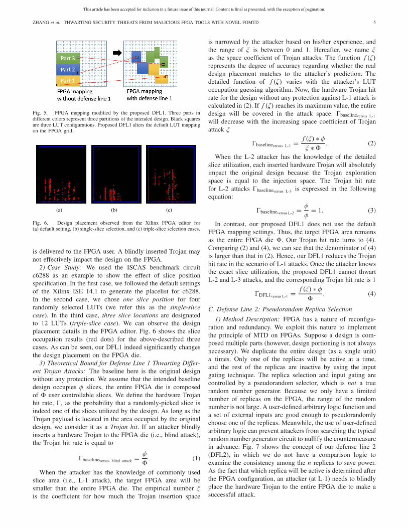
Fig. 5. FPGA mapping modified by the proposed DFL1. Three parts indifferent colors represent three partitions of the intended design. Black squaresare three LUT configurations. Proposed DFL1 alters the default LUT mappingon the FPGA grid.
Fig. 6. Design placement observed from the Xilinx FPGA editor for(a) default setting, (b) single-slice selection, and (c) triple-slice selection cases.
is delivered to the FPGA user. A blindly inserted Trojan maynot effectively impact the design on the FPGA.
2) Case Study: We used the ISCAS benchmark circuitc6288 as an example to show the effect of slice positionspecification. In the first case, we followed the default settingsof the Xilinx ISE 14.1 to generate the placelist for c6288.In the second case, we chose one slice position for fourrandomly selected LUTs (we refer this as the single-slicecase). In the third case, three slice locations are designatedto 12 LUTs (triple-slice case). We can observe the designplacement details in the FPGA editor. Fig. 6 shows the sliceoccupation results (red dots) for the above-described threecases. As can be seen, our DFL1 indeed significantly changesthe design placement on the FPGA die.
3) Theoretical Bound for Defense Line 1 Thwarting Differ-ent Trojan Attacks: The baseline here is the original designwithout any protection. We assume that the intended baselinedesign occupies φ slices, the entire FPGA die is composedof � user controllable slices. We define the hardware Trojanhit rate, �, as the probability that a randomly-picked slice isindeed one of the slices utilized by the design. As long as theTrojan payload is located in the area occupied by the originaldesign, we consider it as a Trojan hit. If an attacker blindlyinserts a hardware Trojan to the FPGA die (i.e., blind attack),the Trojan hit rate is equal to
�baselineversus blind attack = φ
�. (1)
When the attacker has the knowledge of commonly usedslice area (i.e., L-1 attack), the target FPGA area will besmaller than the entire FPGA die. The empirical number ξis the coefficient for how much the Trojan insertion space
is narrowed by the attacker based on his/her experience, andthe range of ξ is between 0 and 1. Hereafter, we name ξas the space coefficient of Trojan attacks. The function f (ξ)represents the degree of accuracy regarding whether the realdesign placement matches to the attacker’s prediction. Thedetailed function of f (ξ) varies with the attacker’s LUToccupation guessing algorithm. Now, the hardware Trojan hitrate for the design without any protection against L-1 attack iscalculated in (2). If f (ξ) reaches its maximum value, the entiredesign will be covered in the attack space. �baselineversus L-1
will decrease with the increasing space coefficient of Trojanattack ξ
�baselineversus L-1 = f (ξ) ∗ φ
ξ ∗ �. (2)
When the L-2 attacker has the knowledge of the detailedslice utilization, each inserted hardware Trojan will absolutelyimpact the original design because the Trojan explorationspace is equal to the injection space. The Trojan hit ratefor L-2 attacks �baselineversus L-3 is expressed in the followingequation:
�baselineversus L-2 = φ
φ= 1. (3)
In contrast, our proposed DFL1 does not use the defaultFPGA mapping settings. Thus, the target FPGA area remainsas the entire FPGA die �. Our Trojan hit rate turns to (4).Comparing (2) and (4), we can see that the denominator of (4)is larger than that in (2). Hence, our DFL1 reduces the Trojanhit rate in the scenario of L-1 attacks. Once the attacker knowsthe exact slice utilization, the proposed DFL1 cannot thwartL-2 and L-3 attacks, and the corresponding Trojan hit rate is 1
�DFL1versus L-1 = f (ξ) ∗ φ
�. (4)
C. Defense Line 2: Pseudorandom Replica Selection
1) Method Description: FPGA has a nature of reconfigu-ration and redundancy. We exploit this nature to implementthe principle of MTD on FPGAs. Suppose a design is com-posed multiple parts (however, design portioning is not alwaysnecessary). We duplicate the entire design (as a single unit)n times. Only one of the replicas will be active at a time,and the rest of the replicas are inactive by using the inputgating technique. The replica selection and input gating arecontrolled by a pseudorandom selector, which is not a truerandom number generator. Because we only have a limitednumber of replicas on the FPGA, the range of the randomnumber is not large. A user-defined arbitrary logic function anda set of external inputs are good enough to pseudorandomlychoose one of the replicas. Meanwhile, the use of user-definedarbitrary logic can prevent attackers from searching the typicalrandom number generator circuit to nullify the countermeasurein advance. Fig. 7 shows the concept of our defense line 2(DFL2), in which we do not have a comparison logic toexamine the consistency among the n replicas to save power.As the fact that which replica will be active is determined afterthe FPGA configuration, an attacker (at L-1) needs to blindlyplace the hardware Trojan to the entire FPGA die to make asuccessful attack.

This article has been accepted for inclusion in a future issue of this journal. Content is final as presented, with the exception of pagination.
6 IEEE TRANSACTIONS ON VERY LARGE SCALE INTEGRATION (VLSI) SYSTEMS
Fig. 7. Schematic of proposed DFL2.
Fig. 8. Hardware Trojan attack exploration space for (a) design place-ment with default FPGA setting and (b) design protected with FOMTDDFL1 and DFL2.
2) Theoretical Bound for Defense Line 2 Thwarting Differ-ent Trojan Attacks: Fig. 8 depicts an example of explorationexpansion by our proposed DFL2. A complete design (includ-ing replication) consists of multiple units, and the control logicfor replica selection is small enough (compared to φ) to beignored for the simplicity of analysis. Because of the sliceposition specification, the rough size of the Trojan explorationspace SFOMTD can be expressed by the following equation:
SFOMTD = max(|Xi − Xk |) ∗ max(|Yk − Y j |). (5)
Compared to the baseline, our method achieves the theoreti-cal worst case hardware Trojan hit rate for L-2 and L-3 attacks,as described in (6) and (7), respectively. If the L-2 attacksare taken place in the design, �baselineversus L-2 increases to 1.In contrast, �DFL1&2versus L-2 remains low due to the expandedTrojan exploration space by the DFL2. The exact Trojan hitrate depends on the size of the design unit for duplication, ν.Equation (6) is greater than (φ/SFOMTD). Under the conditionof L-3 attacks, our Trojan hit rate will not go beyond 1/n(theoretically, the worst case Trojan hit rate is a uniformdistribution of random replica selections). In our simulationsection, we observed that our actual Trojan hit rate never
Fig. 9. Schematic of the Hot-swappable submodule assembling techniqueprovided by the proposed DFL3.
reaches this upper bound
�DFL1&2versus L-2 = φ
n ∗ ν + (φ − ν)(6)
�DFL1&2 versus L-3 = φ
n ∗ φ= 1
n. (7)
D. Defense Line 3: Runtime Design Assembling
1) Method Description: Our defense line 3 (DFL3) is thehot-swappable submodule assembling technique, as shownin Fig. 9. We partition the original design into m submodules,and each submodule is duplicated by n times. Only onereplica of each submodule will be assembled into a completedesign. The pseudorandom selector is utilized to determinewhich replica to be chosen at runtime. After a period oftime, the selection of submodule replicas will be changedwithout stopping the normal operation (i.e., hot-swappableassembling). The maximum number of design configurationsis nm . This large number of configurations further increasesthe difficulty for the attacker to recognize the entire design forattack.
The hot-swappable assembling technique shown in Fig. 9is directly applicable for combinational circuits. We tailor thistechnique to make it suitable for sequential circuits. As shownin Fig. 10, two styles are available for the circuit composed ofcombinational logic and memory elements. In style I, we donot duplicate the registers so that the submodule assemblingtechniques for combinational and sequential circuits are thesame. In style II, the registers have replicas, too. To realizethe hot-swappable feature, we copy the content of activeregisters to the hot-swap registers [(HS Reg.) in Fig. 10] beforethe runtime submodule swapping happens. Then, we load thevalue saved in HS Reg. to all register replicas to resume theoperation after runtime submodule swapping.
a) Additional option 1 (input gating): To thwartL-3 attacks, we could further strengthen our DFL3 by loosingthe input gating and enabling two replicas active, such that thetwo replicas can be used to examine the consistency betweentheir final outputs. However, the enhanced defense capabilitycomes with more power consumption.
b) Additional option 2 (gate replacement on replicas): Todefeat L-3 attacks better, we enhance our DFL3 by bringing

This article has been accepted for inclusion in a future issue of this journal. Content is final as presented, with the exception of pagination.
ZHANG et al.: THWARTING SECURITY THREATS FROM MALICIOUS FPGA TOOLS WITH NOVEL FOMTD 7
Fig. 10. Two styles of applying DFL3 to sequential circuits.
Fig. 11. Gate replacement for the security enhancement in DFL3.
diversity to the replicas of hot-swappable submodules. In thework [18], the diversity on implementation is introduced byusing different hard macros that are obtained by applying dif-ferent constraint conditions during FPGA synthesis. Inspiredby that work, we create hard macros at gate level so thatwe have more flexibility to facilitate the implementation ofheterogeneous replicas for submodules. Those gate-level hardmacros are used to replace some gates in one of the replicas.As a result, even if an attacker searches for the same FPGAconfiguration patterns between two replicas, the success rateof finding two identical copies for future Trojan insertion willbe extremely low.
The flowchart for the proposed gate replacement on replicasis depicted in Fig. 11. First, we randomly choose one (or more)type(s) of logic gates, for instance, NAND (c, a, b), in onereplica. Next, we apply the de Morgan’s laws to replace thechosen gate with other types of logic gates while maintainingthe same Boolean function. For the two-input NAND gate,we can replace it with OR (c, ∼a, ∼b). Note that all the gatereplacements are done in the Verilog description. To preventthe FPGA synthesis tool from removing our gate replacementduring the logic optimization process, we implement theOR (c, ∼a, ∼b) with three customized hard macros, HM_OR
(a, b, c), HM_NOT (a, a), and HM_NOT (b, b). HM_OR
and HM_NOT defined in Verilog work as the logic OR andinversion operations. By using the hard macros, the gates forreplacement can be mapped into one independent slice, and
they will not be merged with other LUT configuration. We canconduct gate replacement for one or multiple replicas so thatthe identical LUT configurations will be removed. Hence, ourenhanced DFL3 can thwart the L-3 attacks.
2) Theoretical Bound for Defense Line 3 Thwarting Dif-ferent Trojan Attacks: With the DFL3, we can obtain nm
configurations in total. Given a design, more submodules leadto more dynamic configurations and, thus, more unpredictabil-ity for Trojan insertion. The coefficient ξi varies for eachconfiguration and so does f (ξi ). To obtain the Trojan hitconsistently, the overall Trojan hit rate for L-1 attacks is asexpressed in (8), in which sp is the number of hot-swappingconfigurations. As the slides for the nonduplicated portion ofthe design change in each FPGA configuration, the overallTrojan hit rate is the product of the Trojan hit rate for spdifferent hot-swapping configurations. The maximum valueof sp is nm
�DFL3versus L-1 =nm∏
i=1
(f (ξi ) ∗ φ
�
)sp
. (8)
With respect to the L-2 attacks, the attacker knows whichslices are occupied by the design but cannot differentiate whichsubmodule belongs to which replica. Hence, the target slicefor Trojan insertion is not clear. The attacker has to randomlychooses φ slices out of all the occupied slices n ∗ ν + (φ − ν).The corresponding Trojan hit rate for this scenario is expressedby the following equation:
�DFL3versus L-2 =(
φ
n ∗ ν + (φ − ν)
)sp
. (9)
In the L-3 attacks, the attacker has full knowledge ofwhich slices are configured for the design protected withthe DFL3, but he/she could only form the complete designby guessing which submodule replicas will be used. Withoutgate replacement, the corresponding Trojan hit rate is shownin (10), where
∑mi=1 xi is equal to ν. The more swapping
during the runtime operation (i.e., higher sp), the less Trojanhit rate the attacker could achieve
�DFL3versus L-3 =(
(m + 1)! · ∏mi=1 nxi∏m
i=1(n ∗ ν + (φ − ν) − i)
)sp
. (10)
VI. EXPERIMENTAL RESULTS
A. Experimental Setup
In the following experiments, we used the XilinxISE 14.1 design suite to synthesize, PAR the netlist ofISCAS’85 and ISCAS’89 benchmark circuits, and the Amber23 processor core (a23) and the communication controllerEthernet MAC (ethmac) downloaded from the OpenCoreswebsite. The ISCAS circuits were configured for a XilinxSpartan-6 XC6SLX16 FPGA, and the large-scale a23 andethmac circuits were mapped to a Xilinx XC6SLX75 FPGA.The detailed slice utilization of each circuit was analyzedby our Python script to extract the occupied FPGA slicepositions. We used MATLAB to insert hardware Trojansblindly or purposely (depending on the experimental goal)in the extracted placelists to mimic the Trojan injection in

This article has been accepted for inclusion in a future issue of this journal. Content is final as presented, with the exception of pagination.
8 IEEE TRANSACTIONS ON VERY LARGE SCALE INTEGRATION (VLSI) SYSTEMS
Fig. 12. Non-similarity rate achieved by proposed DFL1. The subscripts1s and 3s mean that the locations of a single slice or three slices are specifiedin the user constraints file for the FPGA implementation. On each bar,the central mark indicates the median, and the bottom and top edges of thebox indicate the 25th and 75th percentiles, respectively.
TABLE I
MEDIANS OF NON-SIMILARITY RATE ON FPGA CONFIGURATION
the FPGA mapping and PAR stages and then measured thehardware Trojan hit rate. We assume that only the Trojanshaving payloads in the FPGA slices occupied by the designunder protection will lead to a Trojan hit. The FPGA sliceutilization and worst case delay were obtained from the toolsavailable in the Xilinx design suite.
B. Variation on FPGA Slice Utilization
Variation on slice allocation for a design is critical toensure the high unpredictability offered by our method. Hence,we first examined the impact of our DFL1 on the FPGA sliceutilization. We compared all the slices used by the baselinedesign and the one applied user-specified slice designations.The baseline means the original benchmark circuits withoutany protection. We define a metric non-similarity rate to assessthe slice location difference that has been made by our DFL1.The non-similarity rate represents the ratio of the number ofthe LUT instances being placed to new positions due to ourmethod over the total number of slices used in the baseline.
As shown in Fig. 12, our method achieves an average non-similarity rate in the range of 0.49–0.51. This means, on aver-age, about 50% of the LUT instances for each benchmarkcircuit being placed to different positions on the FPGA die dueto our DFL1. We repeated the simulation on non-similarity ratefor sequential circuits and summarized the median values forall non-similarity rates in Table I. As shown, the proposedDFL1 approximately achieves a non-similarity rate of 0.5.The increase on the number of user specified slice locationsslightly enlarges the variation on the non-similarity rate (butstill close to 0.5). Each non-similarity rate in Fig. 12 and
Fig. 13. Average non-similarity rate for different numbers of reallocatedslices.
Fig. 14. Hardware Trojan hit rate reduction by proposed DFL1 applied inthe benchmark circuits (a) c432, (b) c1355, (c) c1908, (d) c6288, (e) s444,and (f) a23 in the scenario of L-1 attacks.
Table I was based on five test trails. According to our casestudy, the average standard deviation on the median value ofdifferent non-similarity rates is in the range of 0.0070–0.034,which is very small.
Fig. 13 provides the average non-similarity rates for sevenbenchmark circuits (c432, c1355, c1908, c6288, s444, s1488,and s13207) based on five trials. The non-similarity rates areall near 0.5, regardless of the number of reallocated FPGAslices by DFL1. Based on the above-mentioned results, we donot suggest users reallocating more than three slices even forlarge designs.

This article has been accepted for inclusion in a future issue of this journal. Content is final as presented, with the exception of pagination.
ZHANG et al.: THWARTING SECURITY THREATS FROM MALICIOUS FPGA TOOLS WITH NOVEL FOMTD 9
Fig. 15. Hardware Trojan hit rate for (a) c432 and (b) nine benchmarkcircuits suffering from four hardware Trojans inserted via L-2 attacks.
C. Assessment on Attack Resilience
The attack resilience of the baseline and our method arecompared in this section. Three attack levels mentioned inSection III-B are considered in the following assessment.
1) Hardware Trojan Hit Rate for L-1 Attacks: Recall thatthe attackers who execute L-1 attacks do not know the loca-tions of all occupied slices for the design of interest. We var-ied the range of attack exploration space from 5% to 50%of the entire FPGA die. Fig. 14 shows that the proposedDFL1 achieves a lower hardware Trojan hit rate � than thebaseline in a wide range of the attack exploration space. Thisis because our DFL1 makes the LUT placement unpredictableand not targetable for L-1 attackers. The hardware Trojan hitrate for c432, c1908, c6288, s444, and a23 first increases withthe increasing ξ . This is because f (ξ) ∗ φ in (2), the numberof occupied slices falling in the attack space, grows fasterthan ξ ∗ �, the attack space. As the maximum value of f (ξ)is 1, �baseline starts to drop after ξ exceeds a threshold. In ourcase studies, the ξ thresholds for c432, c1355, c1908, c6288,s444, and a23 are 15%, 5%, 15%, 25%, 40%, and 35%,respectively. The case of c1355 has a smaller ξ thresholdthan the other benchmark circuits, so we do not observe thatthe corresponding �baseline increases with ξ . The hardwareTrojan hit rate of our method increases much slower with theincreasing ξ than the baseline. When the attack exploration
Fig. 16. Hardware Trojan hit rate for (a) c432 and (b) nine benchmarkcircuits suffering from four hardware Trojans inserted via L-3 attacks.
space is large enough to cover the entire design placed onthe FPGA die, the Trojan hit rate of proposed method willapproach to the Trojan hit rate of the baseline eventually.
2) Hardware Trojan Hit Rate for L-2 Attack: Different fromL-1 attacks, L-2 attacks are able to retrieve the exact locationsof the occupied slices. Consequently, the baseline design doesnot have any resilience against L-2 attacks. The proposedDFL2 activates one complete design replica according tothe pseudorandom selection, and the DFL3 assembles thehot-swappable submodules at runtime. Here, we used twodesign replicas and each replica composed of four submodules.Our simulation indicates that DFL2 and DFL3 further increasethe unpredictability of the truly activated design copy andachieve a lower Trojan hit rate than the baseline. As shownin Fig. 15(a), the baseline yields a hardware Trojan hit rateof 1, which means that the Trojans are always injected to theoccupied slices. In contrast, our DFL2 and DFL3 significantlyreduce the Trojan hit rate over the baseline, especially forthe small number of injected Trojans. When more Trojansare placed in the utilized FPGA slices, our Trojan hit rateeventually increases due to the limited number of replicasavailable in the design.
We examined the Trojan hit rate for nine benchmark circuitsthat suffer from four Trojan insertions via L-2 attacks. Eachhardware Trojan hit rate was obtained from 10 000 test cases.

This article has been accepted for inclusion in a future issue of this journal. Content is final as presented, with the exception of pagination.
10 IEEE TRANSACTIONS ON VERY LARGE SCALE INTEGRATION (VLSI) SYSTEMS
Fig. 17. Comparison of the number of Trojan hits for without and withgate replacement to thwart L-3 pattern searching attack. (a) Exact matching.(b) Approximate matching.
Fig. 18. Comparison of hardware Trojan hit rate for without or with proposedgate replacement to thwart L-3 pattern searching attack. (a) Exact matching.(b) Approximate matching.
The average Trojan hit rate of DFL2 (DFL3) is 71% (38%).As shown in Fig. 15(b), the DFL2 reduces the hit rate by upto 40% over the baseline. The reduction on the Trojan hit ratecan be further improved to 91% with DFL3.
3) Hardware Trojan Hit Rate for L-3 Attack: L-3 attackscan recognize the multiple replicas of the design by searchingfor the exactly same or approximately similar LUT config-uration. We repeated the same experiments as we did forSection VI-C2, except with a different attack level. For the
Fig. 19. Impact of number of hot swaps on hardware Trojan hit rate forc432 under (a) L-2 and (b) L-3 attacks.
Fig. 20. Impact of number of hot swaps on hardware Trojan hit rate for ninebenchmark circuits affected by four hardware Trojans inserted via (a) L-2 and(b) L-3 attacks.
sequential circuits, s1488 and s13207, they were implementedin style I. As shown in Fig. 16(a), the Trojan hit rate for thedesign under L-3 attacks increases with the increasing numberof Trojans. This trend is similar with that for the L-2 attackcase. However, the average Trojan hit rate of DFL2 (DFL3)against L-3 attacks increases to 76% (48%), which is higherthan in the scenario of L-2 attacks. As shown in Fig. 16(b),the DFL2 reduces the hit rate by up to 35% over the baseline.The DFL3 further improves the attack resilience by up to72%. From Figs. 15(b) and 16(b), we can also conclude thatthe L-3 attacks indeed are more powerful than L-2 attacks.This is because L-3 attacks can search for the matched LUTconfiguration patterns.
Fig. 17(a) shows that the average number of exactly matchedLUT configurations per each benchmark circuit is close to 100

This article has been accepted for inclusion in a future issue of this journal. Content is final as presented, with the exception of pagination.
ZHANG et al.: THWARTING SECURITY THREATS FROM MALICIOUS FPGA TOOLS WITH NOVEL FOMTD 11
Fig. 21. Impact of the number of (a) replicas n and (b) submodules m onhardware Trojan hit rate for c6288 affected by the four hardware Trojans.
Fig. 22. Comparison of hardware Trojan hit rate for the proposed DFL3 andDMR affected by four Trojans inserted via (a) L-2 and (b) L-3 attacks.
(i.e., 1). If the attackers search for the LUT configurationsthat have a similar format but use different input/out pins(i.e., approximate matching), the number of matched casesincreases. To address this issue, we applied the gate replace-ment technique to the DFL3. As can be seen from Fig. 17(a),our enhanced method can increase the number of exact match-ing LUT configurations so that the same LUT configurationsdo not stand for the identical logic function for the benchmarkcircuit any more. Therefore, when an attacker performs theL-3 attack, the Trojan hit rate of our method can be reduced.Not only increasing the number of exact matching cases,our gate replacement technique also increases the numberof approximate matching patterns, as shown in Fig. 17(b).As a result, our enhanced DFL3 reduces the hardware Trojanhit rate. From Fig. 18, we can see that the proposed gatereplacement technique reduces the Trojan hit rate for differentcircuits. On average, our method makes the Trojan hit ratedecrease by 62% and 88% for the attacker searching for exactmatching and approximate matching configurations, respec-tively.
D. Dependent Design Factors for Trojan Hit Rate Reduction
In the proposed DFL3, our method swaps the replicasof submodules at runtime. We examined the impact of thenumber of hot swaps on the Trojan hit rate. As depictedin Fig. 19(a) and (b), a larger number of hot swaps used in thedesign yield a lower hardware Trojan hit rate. However, as thenumber of inserted hardware Trojans increases, the Trojanhit rate reduced by hot swapping gradually decreases. Thisconclusion applies to all the benchmark circuits we tested, andit remains consistent with the scenario of L-3 attacks shownin Fig. 20(a) and (b).
TABLE II
IMPACT OF NUMBER OF SUBMODULES (m) ON FPGA COST AND DELAY
TABLE III
NUMBER OF FPGA LUTS UTILIZED BY DIFFERENT METHODS
The impacts of the number of replicas n and submodulesm on the Trojan hit rate are shown in Fig. 21(a) and (b),respectively. The increase on n helps to reduce the hardwareTrojan hit rate, as a larger n yields more unpredictability forattackers. The reduction on the Trojan hit rate becomes morenoticeable if more hardware Trojans are injected to the design.The impact of m on the Trojan hit rate is not as significant asthe impact from n [which is also indicated by the mathematicalanalysis in (10)]. However, the number of submodules in theoriginal design will slightly affect the area overhead, as shownin Table II. The overhead on the worst case delay varies,depending on how the submodules are divided. In general,more submodules lead to an increase on the delay. The resultsin Table II are based on the DFL3 without gating techniqueand the replica number of 2.
E. Assessment on Hardware Cost, Delay, and Power
The following experiments are based on the following setup:the replicas for DFL2 and DFL3 were two, each circuit wasdivided into four submodules, the style I was applied to DFL3,and four hot swappings were conducted during simulation.
1) Hardware Utilization: Table III summarizes the numberof utilized LUTs for different methods. Since our DFL1 onlychanges the location of designated slices, on average, ourmethod consumes 0.33% more LUTs than the baseline.In DFL2, we duplicated the design under protection once andutilized a pseudorandom selection unit for replica selection.The unselected replica was muted through input gating. Forthe small circuits, the increase on the LUT utilization couldbe large due to the relative large size of pseudorandomselection and input gating. However, when the object forprotection is large, the FPGA overhead can be reduced throughoptimization. The LUT overheads for the largest combinationalcircuit c6288 and sequential circuit s13207 in our case studiesare 111.9% and 138.3%, respectively.

This article has been accepted for inclusion in a future issue of this journal. Content is final as presented, with the exception of pagination.
12 IEEE TRANSACTIONS ON VERY LARGE SCALE INTEGRATION (VLSI) SYSTEMS
TABLE IV
TOTAL POWER CONSUMPTION BY DIFFERENT METHODS. UNIT: μW
Fig. 23. Comparison of the number of exact matching on LUT configuration.
During the hot-swapping process, our DFL3 without inputgating (i.e., DFL3.G) interleaved multiple sections of the orig-inal design and its replicas. In addition to the primary inputs,the input gating technique was also applied to the inputsfor hot-swappable submodules. As a result, the LUT over-heads for c6288 and s13207 increase to 116.8% and 145%,respectively. If we remove the input gating (i.e., NG) option,the corresponding overheads on the utilized LUTs for thelargest circuits are reduced to 110.9% and 140.6%, respec-tively. Certainly, removing the input gating will cost morepower consumption. Although our DFL3 incurs comparableLUT utilization for double modular redundancy (DMR), ourruntime replica selection ensures lower power consumptionand provides better unpredictability. We also examined thehardware utilization on the large-scale circuits a23 and ethmac.Our experiments indicated that the overheads on LUT utiliza-tion for a23 and ethmac are 196.4% (212.4%) and 119.3%(156.3%) for DFL2 (DFL3), respectively.
2) Power Consumption: We synthesized the Verilog codesfor the benchmark circuits in the Synopsys Design Compiler.The clock frequency was set to 100 MHz for each design.We measured the power consumption in the tool DesignCompiler and reported in Table IV. On average, the proposedDFL2 leads to an increase on the total power by 8.86%over the baseline. Our DFL3 with input gating providesbetter resilience against advanced attacks, at the cost of 11%more total power than the baseline. The increased powerconsumption is due to the pseudorandom selection and inputgating logic, as well as the multiplexers before the finaloutputs.
3) Worst Case Delay: We measured the worst case delaysfor different designs using the PlanAhead tool in Xilinx ISE14.1 design suite. As shown in Table V, slice designation usedin the proposed DFL1 could lead to more or less worst casedelay, depending on where the slice is designated. To examinethe impact of the slice designation on the worst case delay,
Fig. 24. Comparison of the power consumption between the proposedDFL3 and DMR.
Fig. 25. FPGA output for the circuit protected with (a) proposed DFL3 and(b) ATMR [18].
we varied the number of designated slices from 1 to 3 andperformed five test cases for each designation condition. Basedon our case studies, DFL1 induces a delay overhead aslarge as 1.74% and 3.52% for the single-slice designationand triple-slice designation, respectively. Given a tight timingbudget, several slice selections should be examined for the bestslice reallocation in terms of incurring minor delay overhead.Compared to the baseline, our DFL2 leads to the worst casedelay increase in the range of 4.23%–17.19% for differentbenchmark circuits. Due to the hot-swappable logic, the delayoverhead induced by DFL3 is no more than 22.02%. For thelarge-scale benchmark circuits a23 (ethmac), the DFL2 incurs4.4% (6.2%) more delay than the baseline. Our DFL3 causesthe worse-case delay increase by 16% and 8.3% over thebaseline for a23 and ethmac, respectively.
F. Comparing FOMTD With Static Trojan Detection Method
In this section, we compare our FOMTD with the staticTrojan detection methods that are based on DMR or TMR.Even though the attacker who performs L-2 attacks can seethe utilized LUTs, it is not guaranteed that the attacker can suc-cessfully place two identical hardware Trojans in two designreplicas. Because the Trojans inserted on the replica compar-ison logic cannot be detected by DMR, the Trojan hit rate isnot reduced to zero. When we advance the attack method toL-3 attacks, our DFL3 effectively reduces the Trojan hit rate.Together with the runtime hot-swapping feature, fewer numberof exactly matched LUT configurations available in the netlistof our method benefits us to reduce the success rate of a Trojaninserted by L-2 and L-3 attacks. Fig. 22 shows that our methodachieves a lower Trojan hit rate than DMR. On average, ourDFL3 reduces the Trojan hit rate by 63.3% and 42.5% againstthe L-2 and L-3 attacks, respectively. Indeed, L-3 attacks can

This article has been accepted for inclusion in a future issue of this journal. Content is final as presented, with the exception of pagination.
ZHANG et al.: THWARTING SECURITY THREATS FROM MALICIOUS FPGA TOOLS WITH NOVEL FOMTD 13
TABLE V
COMPARISON OF WORST CASE DELAY. UNIT: ns
search for the identical LUT configurations, but the numberof exactly matched LUT configurations is not high in FPGAmapping (which is different with ASIC design). Fig. 23 showsthat our DFL3 can effectively reduce the number of exactmatching cases over DMR. This explains why DFL3 obtains abetter attack resilience than DMR. Because of the input gating,our DFL3 consumes less power than DMR. As indicatedin Fig. 24, the total power consumption for the five benchmarkcircuits protected with DFL3 is less than that for the circuitsprotected with DMR. On average, our method achieves 50%reduction on the total power over the DMR method.
Next, we applied the proposed method and ATMR [18]to the circuits for a practical application. We connected theXilinx FPGA board to a monitor through a Video GraphicsArray (VGA) cable. The function module configured in theFPGA device was used to draw a chess board on a screenby sending a VGA signal to the monitor. Two hardwareTrojans were inserted to the FPGA placelist by the mean ofL-3 attacks. Our DFL3 was applied to thwart the L-3 attackfrom the untrusted FPGA software. Our method guaranteedthe correct display of the original picture shown in Fig. 25(a).In contrast, the ATMR method did not eliminate the effect ofthe two Trojans, yielding a distorted chess board, as shownin Fig. 25(b). This is because the L-3 attack searches for theidentical LUT configurations in the ATMR design replicas andinserts the Trojans in the identical LUTs, each belonging toone design replica.
VII. CONCLUSION
Many security mechanisms for FPGA-based systems havebeen investigated to prevent systems from IP theft and reverseengineering attack on bitstream. However, there is limitedliterature available that studies the security threats originatedfrom the untrusted FPGA CAD tools. This paper fills thegap. We demonstrate two practical attacks through Xilinxand Altera FPGA design suites. We further classify threeTrojan attack levels, depending on the attacker’s prior FPGAexperience and ability to manipulate the FPGA software.To mitigate the hardware Trojans induced by the maliciousFPGA tools, we propose an FOMTD method that offers three
defense lines. Each defense line generates a different degree ofunpredictability from the malicious FPGA software designer’spoint of view. As our unpredictability is formed after theCAD tool is delivered to FPGA users, our method facilitatesFPGA users to thwart Trojan insertion attacks during theFPGA configuration phase. To the best of our knowledge,our research effort is the first work that investigates theFPGA-based MTD for SRAM FPGAs.
We did extensive evaluation on the security, hardware cost,and performance. The proposed DFL1 changes 50% of thedefault LUT mapping on the FPGA device and reduces thehardware Trojan hit rate of L-1 attacks, at the cost of 0.33%more LUT utilization compared to the baseline. When advanceattacks occur, our defense lines maintain a low Trojan hit rate.DFL2 and DFL3 reduce the Trojan hit rate by up to 40%and 91%, respectively, over the baseline. The gate replac-ing technique in DFL3 further reduces the Trojan hit rate,on average, by 62% and 88% even if the attacker searches forexact and approximate configuration matching, respectively.The power increases due to the DFL2 and DFL3 are 8.86%and 11%, respectively, compared to the baseline. The delayoverhead varies. According to our case studies, the worst casedelay overhead our defense line incurs is 22.02%. We alsocompared the DFL3 to a static Trojan detection method,DMR. Experimental results show that our method improvesthe hardware Trojan hit rate by 63.3% and 42.5% againstL-2 and L-3 attacks, respectively. Because of the input gatingand hot-swappable features in our method, our DFL3 con-sumes 50% less power than DMR.
The limitation of the proposed defense lines is the hardwarecost and delay increase. However, considering the significantimprovement on the resilience against Trojan insertion attacks,the overhead of our method is moderate and acceptable forsecurity-critical applications. In the future work, we will workon the cost minimization of the FOMTD method.
REFERENCES
[1] Global Market Insights Inc. FPGA Market Size Set to Exceed USD 9.98Billion by 2022, With Over 8.4% CAGR from 2015 to 2022. Accessed:Sep. 13, 2018. [Online]. Available: https://goo.gl/uEmByo
[2] Security for Volatile FPGAs. Accessed: Sep. 13, 2018. [Online]. Avail-able: http://www.cl.cam.ac.uk/techreports/UCAM-CL-TR-763.pdf

This article has been accepted for inclusion in a future issue of this journal. Content is final as presented, with the exception of pagination.
14 IEEE TRANSACTIONS ON VERY LARGE SCALE INTEGRATION (VLSI) SYSTEMS
[3] M. Majzoobi, F. Koushanfar, and M. Potkonjak, “FPGA-orientedsecurity,” in Introduction to Hardware Security and Trust.2012, pp. 1–38. [Online]. Available: http://web.cs.ucla.edu/ mio-drag/papers/Majzoobi_2011.pdf
[4] M. Majzoobi and F. Koushanfar, “Time-bounded authenticationof FPGAs,” IEEE Trans. Inf. Forensics Security, vol. 6, no. 3,pp. 1123–1135, Sep. 2011.
[5] I. Hadžic, S. Udani, and J. M. Smith, “FPGA viruses,” in Proc. Int.Workshop FPL, Apr. 1999, pp. 291–300.
[6] S. Trimberger, “Trusted design in FPGAs,” in Proc. DAC, Jun. 2007,pp. 5–8.
[7] S. Skorobogatov and C. Woods, “Breakthrough silicon scanning discov-ers backdoor in military chip,” in Proc. CHES, Sep. 2012, pp. 23–40.
[8] P. Swierczynski, A. Moradi, D. Oswald, and C. Paar, “Physical securityevaluation of the bitstream encryption mechanism of altera stratix II andstratix III FPGAs,” ACM Trans. Reconfigurable Technol. Syst., vol. 7,pp. 34:1–34:23, Dec. 2014.
[9] S. Mal-Sarkar, R. Karam, S. Narasimhan, A. Ghosh, A. Krishna, andS. Bhunia, “Design and validation for FPGa trust under hardwareTrojan attacks,” IEEE Trans. Multi-Scale Comput. Syst., vol. 2, no. 3,pp. 186–198, Jul. 2016.
[10] Z. Zhang, Q. Yu, L. Njilla, and C. Kamhoua, “FPGA-oriented movingtarget defense against security threats from malicious FPGA tools,” inProc. HOST, Apr./May 2018, pp. 163–166.
[11] R. S. Chakraborty, I. Saha, A. Palchaudhuri, and G. K. Naik, “Hard-ware Trojan insertion by direct modification of FPGA configurationbitstream,” IEEE Design Test, vol. 30, no. 2, pp. 45–54, Apr. 2013.
[12] Z. Zhang, L. Njilla, C. Kamhoua, K. Kwiat, and Q. Yu, “SecuringFPGA-based obsolete component replacement for legacy systems,” inProc. ISQED, Mar. 2018, pp. 401–406.
[13] G. Bloom, B. Narahari, R. Simha, A. Namazi, and R. Levy, “FPGASoC architecture and runtime to prevent hardware Trojans from leakingsecrets,” in Proc. HOST, May 2015, pp. 48–51.
[14] A. L. Oliveira, “Techniques for the creation of digital watermarks insequential circuit designs,” IEEE Trans. Comput.-Aided Des. Integr.Circuits Syst., vol. 20, no. 9, pp. 1101–1117, Sep. 2001.
[15] J. Zhang, Y. Lin, Y. Lyu, and G. Qu, “A PUF-FSM bindingscheme for FPGA IP protection and pay-per-device licensing,” IEEETrans. Inf. Forensics Security, vol. 10, no. 6, pp. 1137–1150,Jun. 2015.
[16] R. Karam, T. Hoque, S. Ray, M. Tehranipoor, and S. Bhunia,“MUTARCH: Architectural diversity for FPGA device and IP security,”in Proc. ASPDAC, Jan. 2017, pp. 611–616.
[17] Y. Pino, V. Jyothi, and M. French, “Intra-die process variation awareanomaly detection in FPGAs,” in Proc. ITC, Oct. 2014, pp. 1–6.
[18] S. Mal-Sarkar, A. Krishna, A. Ghosh, and S. Bhunia, “Hardwaretrojan attacks in FPGA devices: Threat analysis and effective countermeasures,” in Proc. GLSVLSI, May 2014, pp. 287–292.
[19] D. M. Shila and V. Venugopal, “Design, implementation and securityanalysis of hardware trojan threats in FPGA,” in Proc. IEEE ICC,Jun. 2014, pp. 719–724.
[20] B. Khaleghi, A. Ahari, H. Asadi, and S. Bayat-Sarmadi, “FPGA-based protection scheme against hardware trojan horse insertion usingdummy logic,” IEEE Embedded Syst. Lett., vol. 7, no. 2, pp. 46–50,Jun. 2015.
[21] S. Bhunia, M. S. Hsiao, M. Banga, and S. Narasimhan, “HardwareTrojan attacks: Threat analysis and countermeasures,” Proc. IEEE,vol. 102, no. 8, pp. 1229–1247, Aug. 2014.
[22] R. S. Chakraborty, F. Wolff, S. Paul, C. Papachristou, and S. Bhunia,“MERO: A statistical approach for hardware Trojan detection,” in Proc.CHES, Aug. 2009, pp. 396–410.
[23] S. Narasimhan et al., “Hardware Trojan detection by multiple-parameterside-channel analysis,” IEEE Trans. Comput., vol. 62, no. 11,pp. 2183–2195, Nov. 2013.
[24] R. Druyer, L. Torres, P. Benoit, P. V. Bonzom, and P. Le-Quere,“A survey on security features in modern FPGAs,” in Proc. ReCoSoC,Jun./Jul. 2015, pp. 1–8.
[25] SoC FPGA Hardware Security Requirements and Roadmap. Accessed:Sep. 13, 2018. [Online]. Available: https://www.intel.com/content/dam/www/programmable/us/en/pdfs/education/ev%ents/northamerica/isdf/SoC-FPGA-Hardware-Security.pdf
[26] M. Tehranipoor and F. Koushanfar, “A survey of hardware Trojantaxonomy and detection,” IEEE Design Test Comput., vol. 27, no. 1,pp. 10–25, Jan. 2010.
[27] J. A. Roy, F. Koushanfar, and I. L. Markov, “Extended abstract: CircuitCAD tools as a security threat,” in Proc. HOST, Jun. 2008, pp. 65–66.
[28] S. M. Trimberger and J. J. Moore, “FPGA security: Motivations,features, and applications,” Proc. IEEE, vol. 102, no. 8, pp. 1248–1265,Aug. 2014.
[29] D. Last, D. Myers, M. Heffernan, M. Caiazzo, and C. N. Paltzer,“Command and control of proactive defense,” J. Cyber Secur. Inf. Syst.,vol. 4, no. 1, pp. 8–13, 2015.
[30] Moving Target Defense. Accessed: Sep. 13, 2018. [Online]. Available:https://www.dhs.gov/science-and-technology/csd-mtd
[31] R. Zhuang, S. A. DeLoach, and X. Ou, “Towards a theory of movingtarget defense,” in Proc. 1st ACM Workshop Moving Target Defense,2014, pp. 31–40.
Zhiming Zhang is currently working toward thePh.D. degree at the Department of Electrical andComputer Engineering, University of New Hamp-shire, Durham, NH, USA.
His current research interests include hardwaresecurity that includes design obfuscation, side chan-nel analysis of encryption algorithms, fault attackanalysis, and emerging technologies with an empha-sis on hardware security and trust.
Laurent Njilla (M’05) received the B.S. degreefrom the Department of Computer Science, Uni-versity of Yaoundé, Yaoundé, Cameroon, the M.S.degree from the University of Central Florida,Orlando, FL, USA, and the Ph.D. degree from theElectrical and Computer Engineering Department,Florida International University, Miami, FL, USA.
He is currently a Research Engineer with the AirForce Research Laboratory, Department of Defense,Rome, NY, USA. His current research interestsinclude cyber security, game theory, hardware and
network security, blockchain technology, cyber threat information, andadvanced computer networking.
Charles A. Kamhoua (S’10–M’12–SM’14)received the B.S. degree in electronics from theUniversity of Douala (ENSET), Douala, Cameroon,in 1999, and the Ph.D. degree in electricalengineering from Florida International University,Miami, FL, USA, in 2011.
She was a Researcher with the U.S. Air ForceResearch Laboratory, Rome, NY, USA, for sixyears, and an educator in different academicinstitutions for over 10 years. He has held visitingresearch positions at the University of Oxford,
Oxford, U.K., and Harvard University, Cambridge, MA, USA. He is currentlya Researcher with the Network Security Branch of the U.S. Army ResearchLaboratory, Adelphi, MD, USA, where he is responsible for conducting anddirecting basic research in the area of game theory applied to cyber security.She has coauthored over 150 peer-reviewed journal and conference papers.He has been recognized for his scholarship and leadership with numerousprestigious awards.
Dr. Kamhoua is currently a member of the FIU Alumni Association andACM and also an Advisor of the National Research Council Post-DoctoralProgram.
Qiaoyan Yu (S’03–M’11–SM’17) received theB.S. degree from Xidian University, Xi’an, China,in 2002, the M.S. degree from Zhejiang University,Hangzhou, China in 2005, and the Ph.D. degreein electrical engineering from the University ofRochester, Rochester, NY, USA, in 2011.
She is currently an Associate Professor with theDepartment of Electrical and Computer Engineer-ing, University of New Hampshire, Durham, NH,USA. Her current research interests include hard-ware security and trust, embedded system security,
cyber-physical system, error control for networks-on-chip, and fault-tolerancefor VLSI circuits and systems.
Dr. Yu is a member of the Editorial Boards of Integration, the VLSI journal,the Microelectronics Journal, and the Journal of Circuits, Systems, andComputers. She was a recipient of the National Science Foundation CAREERAward in 2017. She has served on the Technical Program Committees ofHOST, DAC, FDTC, Asian HOST, ISVLSI, DFT, ASP-DAC, GLSVLSI,and ISCAS.