three-port dc-dc converter for stand-alone photovoltaic ... · addresses the two issues by...
TRANSCRIPT

1
1
Abstract—System efficiency and cost effectiveness are of
critical importance for photovoltaic (PV) systems. This paper
addresses the two issues by developing a novel three-port DC-DC
converter for stand-alone PV systems, based on an improved
Flyback-Forward topology. It provides a compact single-unit
solution with a combined feature of optimized maximum power
point tracking (MPPT), high step-up ratio, galvanic isolation and
multiple operating modes for domestic and aerospace
applications. A theoretical analysis is conducted to analyze the
operating modes followed by simulation and experimental work.
The paper is focused on a comprehensive modulation strategy
utilizing both PWM and phase-shifted control that satisfies the
requirement of PV power systems to achieve MPPT and output
voltage regulation. A 250 W converter was designed and
prototyped to provide experimental verification in term of system
integration and high conversion efficiency.
Index Terms— DC-DC power conversion, maximum power point tracking, phase shift, photovoltaic power system, voltage
control.
I. INTRODUCTION
OLAR energy is a primary and renewable source of energy. As the cost of photovoltaic (PV) panels is seen to
reduce continuously, PV-based power generation is gaining in
__________________________________________________
Manuscript received February 7, 2014; revised March 19, 2014; accepted May 30, 2014.
Y. Hu is with the Department of Electronic and Electrical Engineering, University of Strathclyde, Glasgow, G1 1XQ, U.K.
W. Xiao is with Faculty of Science and Technology, Masdar Institute, Abu Dhabi, UAE.
W. Cao and J. Morrow are with the School of Electronics, Electrical Engineering and Computer Science, Queen’s University Belfast, Belfast, BT9 5AH, U.K. (e-mail: [email protected]).
B. Ji is with the School of Electrical and Electronic Engineering, Newcastle University, Newcastle upon Tyne, NE1 7RU, U.K.
Color versions of one or more of the figures in this paper are available online at http://ieeexplore.ieee.org.
popularity for both grid-connected and stand-alone systems [1]-[5]. Currently, the global installation is over 40 GW and increases at an annual rate of 50% since 2005 [6].
Stand-alone systems are independent of utility grids and commonly employed for satellites, space stations, unmanned aerial vehicles (UAV) and domestic applications [7]-[10]. Such systems require storage elements to accommodate the intermittent generation of solar energy [11]-[15]. Over the years, research effort has been directed toward improving the power conversion efficiency as well as the power density by weight (PDW) and the power density by volume (PDV) [16][17].
Traditionally, the two-port topology utilizes the dual active bridges (DAB) [18]-[21] and the half or full bridges can support the multiport structure to some extent [22]-[25]. A combination of Flyback-Forward converter with full bridge has shown some advantages in zero voltage switching (ZVS) and high conversion ratio for fuel cell applications [26]. A modified half bridge converter is reported in [27] which consists of one PV input port, one bidirectional battery port, and an isolated output for satellite applications. However, in these converters, a multi-input-multi-output (MIMO) solution is generally difficult to achieve for power electronic applications.
In theory, multiple-input converters (e.g. three-port converters) can provide a single-unit solution interfacing multiple energy sources and common loads [28]-[30]. They perform better than traditional two-port converters due to their lower part count and smaller converter size. In particular, the isolated three-port converter (ITPC) has become an attractive topology for various applications owing to their multiple energy source connection, compact structure and low cost [31]-[33]. In this topology, a simple power flow management scheme can be used since the control function is centralized. A high-frequency transformer can provide galvanic isolation and flexible voltage conversion ratio. The ITPC is usually
Yihua Hu, Member, IEEE, Weidong Xiao, Member Wenping Cao, Senor Member, IEEE, Bing Ji, Member, IEEE, D. John Morrow, Member, IEEE
Three-Port DC-DC Converter for Stand-Alone Photovoltaic Systems
S
2
2
integrated into an individual converter such as forward, push-pull, full bridge, and Flyback converters [34][35].
The ITPC utilizes the triple active bridges (TAB) with inherent features of power controllability and ZVS. Their soft-switching performance can be improved if two series-resonant tanks are implemented [36]. An advanced modulation strategy is reported in [37] which incorporates a phase shift (PS) and a PWM to extend the operating range of ZVS. Nonetheless, the TAB topology suffers from the circuit complexity using three active full bridges or half bridges and the power loss caused by reactive power circulation. Therefore a Buck-Boost converter is proposed [38] to integrate a three-port topology in the half bridge and to decompose the multivariable control problem into a series of independent single-loop subsystems. By doing so, the power flow in each loop can be independently controlled. The system is suitable for PV-battery applications since one converter interfaces the three components of the PV array, battery, and loads. However, in each energy transfer state, current passes through at least five inductor windings, especially under high switching frequency conditions, giving rise to power loss; its peak efficiency is less than 90% and its power capability is limited by the transformer design, making it impossible for current sharing.
Based on these topologies, a new three-port DC-DC converter is developed in this paper to combine a new ITPC topology and an improved control strategy, and to achieve decoupled port control, flexible power flow and high power capability while still making the system simple and cheap.
II. TOPOLOGY AND OPERATION
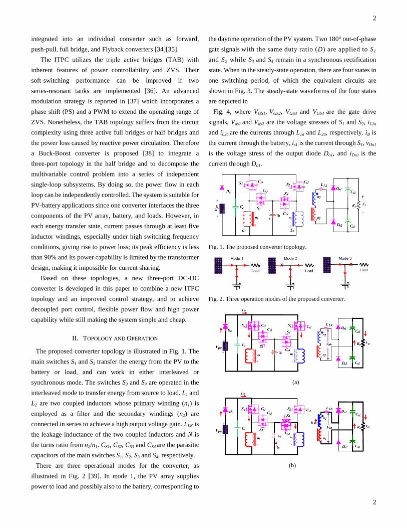
The proposed converter topology is illustrated in Fig. 1. The main switches S1 and S2 transfer the energy from the PV to the battery or load, and can work in either interleaved or synchronous mode. The switches S3 and S4 are operated in the interleaved mode to transfer energy from source to load. L1 and L2 are two coupled inductors whose primary winding (n1) is employed as a filter and the secondary windings (n2) are connected in series to achieve a high output voltage gain. LLK is the leakage inductance of the two coupled inductors and N is the turns ratio from n2/n1. CS1, CS2, CS3 and CS4 are the parasitic capacitors of the main switches S1, S2, S3 and S4, respectively.
There are three operational modes for the converter, as illustrated in Fig. 2 [39]. In mode 1, the PV array supplies power to load and possibly also to the battery, corresponding to
the daytime operation of the PV system. Two 180° out-of-phase gate signals with the same duty ratio (D) are applied to S1 and S2 while S3 and S4 remain in a synchronous rectification state. When in the steady-state operation, there are four states in one switching period, of which the equivalent circuits are shown in Fig. 3. The steady-state waveforms of the four states are depicted in
Fig. 4, where VGS1, VGS2, VGS3 and VGS4 are the gate drive signals, Vds1 and Vds2 are the voltage stresses of S1 and S2, iL1a and iL2a are the currents through L1a and L2a, respectively. iB is the current through the battery, is1 is the current through S1, vDo1 is the voltage stress of the output diode Do1, and iDo1 is the current through Do1.
Fig. 1. The proposed converter topology.
Fig. 2. Three operation modes of the proposed converter.
(a)
(b)

3
3
Vpv
S1 Cs1
n1
*
n
S2 Cs2
S3
Cs3 S4
Cs4
+
- VB
•
n1
Do
Cc
i in
*
n2
n2
VoRo
Co1Do1
Do2 Co2
L Lk
Vab
(c)
(d)
Fig. 3. Four operating states of the proposed converter in mode 1.
Vgs1
iL1a
iS1
vds1
vDo1
iL2aiL1a
t0 t1 t2 t3 t4
Vgs1
Vgs2
iL2a
iDo1
Vgs2
Vgs1
Vgs2
vds1iS1
iDo1
vDo1
ib
Vgs3
Vgs4
Fig. 4. Waveforms of the proposed converter under mode 1.
State 1 [t0-t1]: The main switches S1 and S2 are both in turn-on state before t0. The two coupled inductors work in the flyback state to store energy from the PV array. The output rectifier diodes Do1 and Do2 are both reverse-biased. The energy stored in the secondary output capacitors Co1 and Co2 transfers to the load.
State 2 [t1-t2]: At t1, S2 turns OFF, S4 turns ON, while the diodes Do1 is ON. The primary side of the coupled inductor L2 charges the battery through S4. During this state, L1 operates in the forward mode and L2 operates in the flyback mode to transfer energy to the load. When S1 turns on and S2 turns off, the primary voltage of the coupled inductor L1 is Vpv and the voltage on L2 is –VB.
According to the voltage balance law,
(1 )= −PV BDV D V (1)
1 ( ) Bab B B
NVDV N V N VD D−
= − − = (2)
State 3 [t2-t3]: At t2, S2 turns ON, which forces the two coupled inductors work in the flyback state to store energy and Do2 is reverse-biased. The energy stored in Co1 and Co2 transfers to the load. At t3, the leakage inductor current decreases to zero and the diode Do1 turns OFF.
State 4 [t3-t4]: At t3, S1 turns OFF and S3 turns ON, which turns Do2 ON. The primary side of coupled inductor L1 charges the battery through S3. During this state, L2 operates in the forward mode and L1 operates in the flyback mode to transfer energy to the load. When S1 turns ON and Do2 turns OFF, followed by a new switching period.
In mode 2, the battery supplies power to the load, as shown in Fig. 5(a), indicating the nighttime operation of the stand-alone system. The circuit works as the Flyback-Forward converter, where S3 and S4 are the main switches, Cc, S1 and S2 form an active clamp circuit. When the load is disconnected, the stand-alone system enters into mode 3. The PV array charges battery without energy transferred to the load due to the opposite series connected structure of the coupled inductor (see Fig. 5b). S1 and S2 work simultaneously and the topology is equivalent to two paralleled Buck-Boost converters.
(a) Mode 2
(b) Mode 3
Fig. 5. Converter operating modes 2 and 3.
III. PERFORMANCE ANALYSIS AND FEEDBACK LOOP DESIGN
In order to realize flexible energy flow control, the modulation strategy is proposed to combine PWM with PS
Vpv
*
n2
n2
S1
VoRo
Co1Do1
Do2 Co2
L LkCs1
n1
*
n
S2 Cs2
S3
Cs3 S4
Cs4
+
- VB
•
Vab
n1
Do
Cc
iLK
iB
i in
**
+
-
•
Do
n1
Cc
VB
n2
n2
VoRo
Co1Do1
Do2 Co2
LLk
n1
L1 L2
S1 S2
4S
Vpv
+
-+
-
Cs2Cs1
S3
Cs3
Cs4
**
+
-
•
Do
n1
Cc
VB
n2
n2
VoRo
Co1Do1
Do2 Co2
LLk
n1
L1 L2
S1 S2
4S
Vpv
+
-+
-
Cs2Cs1
S3
Cs3
Cs4

4
4
schemes. Firstly, the relationship of voltage gains with duty ratio and PS needs to be derived. In the following analysis, S1 and S2 have the same duty ratio D, whilst S3 and S4 share another duty ratio. The gate signals for S1 and S3 are complementary, and so are S2 and S4.
A. Analysis of Circuit Performance for D≥0.5
When the duty cycle D≥0.5, there are five operating cases which need to be analyzed, as shown in Fig. 6.
(a) Case 1 (b) Case 2
(c) Case 3 (d) Case 4
(e) Case 5
Fig. 6. Five operational cases for D ≥ 0.5.
In case 1, the phase shift angle is between 0 and φcrit1. From the waveform of the leakage inductor current, the secondary side of the coupled inductor is equivalent to a discontinuous conduction mode (DCM) of a Buck converter. When φ=φcrit1, the current pulses A and B is in a boundary conduction mode, as shown in Fig. 7.
For pulse A, the current decreases to the negative peak value and increases to zero at the time of (1-D)Ts. The decrement time
is equal to and the increment time is
. Following the voltage-second balance
(Eq. 3), the critical phase angle can be determined by Eq. 4.
(a) Signal waveforms (b) Equivalent circuit at φ=φcrit1
Fig. 7. System operation in Case 1.
(3)
(4)
The secondary side of the coupled inductor is equivalent to two Buck converters connected in parallel at the DCM operational condition. The corresponding equivalent duty ratio of the Buck converter is φ/2π. Provided the voltage gain of the Buck converter in DCM, the output voltage is given by:
(5) In case 2, the phase shift angle is between φcrit1 and φcrit2. φcrit2
is the transition point from a continuous conduction mode (CCM) to a DCM, which can be determined by Eq. 6. The voltage equations at φcrit1 and φcrit2 are derived by Eqs. 7 and 8.
(6)
(7)
(8) In case 3, the angle shifts from φcrit2 to φcrit3. The duty ratio of
the secondary side of the Buck converter stays constant, and the voltage gain reaches the highest. Therefore, the critical point, φcrit3, and the corresponding voltage can be calculated by Eqs. 9 and 10. φcrit3 is the boundary point between DCM and CCM. With the increase in the PS angle, the voltage declines. In this case, the output voltage cannot be controlled by PS, as suggested by Eq. 11.
(9)
(10)

5
5
2
224 21 1
(1 ) / 2
Bo
k
o s
NVVDL
R T D
= ⋅ ⋅⋅
+ +⋅ ⋅ − (11)
In case 4, the PS angle ranges from φcrit3 to φcrit4. The leakage inductor current is still higher than zero before next voltage pulse. φcrit4 is the boundary point between DCM and CCM. The critical point, φcrit4 and the corresponding voltage can be expressed as Eqs. 12 and 13.
4 1 2crit critϕ π ϕ= − (12)
4(1 ) (1 )2 2crit o
k k
VNV DDL L
ϕπ
− = − (13)
In case 5, the phase shift angle increases from φcrit4 to 2π. The duty ratio of the secondary side Buck converter is 1-φ/2π. The output voltage can be given by
2
2 24 21 1
(1 / 2 ) / 2
Bo
k
o s
NVVDL
R T ϕ π
= ⋅ ⋅⋅
+ +⋅ ⋅ −
(14)
B. Analysis of Circuit Performance for D<0.5
Similarly, there are five operating cases for D<0.5. The respective waveforms are shown in Fig. 8.
S3 S1
S2 S4
D
φ
S1 S3 S1
NVB/D
S2 S4 S2
Vab
iLkt
S3 S1
S2 S4
D
φ
S1 S3 S1
NVB/D
S2 S4S4
Vab
iLkt
(a) Case 1 (b) Case 2
S3 S1
S2 S4
D
φ
S1 S3 S1
NVB/D
S2 S4S4
Vab
iLkt
S3 S1
S2 S4
D
φ
S1 S3 S1
NVB/D
S4 S2 S4
Vab
iLkt
(c) Case 3 (d) Case 4
S3 S1
S2 S4
D
φ
S1 S3 S1
NVB/D
S4 S2 S4
Vab
iLkt
(e) Case 5
Fig. 8. Five cases under D < 0.5.
In Case 1 (0<φ<φcrit1), considering the waveform of the leakage inductor current, the secondary side of the coupled inductor is equivalent to a DCM Buck converter, the corresponding duty ratio is D=φ/2π. Thus the critical angle and the output voltage are:
21 o
critB
VD
N Vϕ π= ⋅ ⋅
⋅ (15)
2
2 24 21 1( / 2 ) / 2
Bo
k
o s
NVVDL
R T ϕ π
= ⋅ ⋅⋅
+ +⋅ ⋅
(16)
In case 2 (φcrit1<φ<φcrit2), the leakage inductor current is still above zero. The system equations can be expressed as
2 4 Bcrit
o
N VV
ϕ π⋅
= ⋅ (17)
1 2 2crit oB
k k
VNV DDL L
ϕπ
⋅ = ⋅ (18)
2 2 2
o critB
k k
VNV DDL L
ϕπ
⋅ = (19)
In case 3 (φcrit2<φ<φcrit3), the duty ratio of the secondary winding is equal to D. The system equations are
3 2 2crit critϕ π ϕ= − (20)
3(1 )2 2
o critB
k k
VNV DDL L
ϕπ
⋅ = − (21)
2
2 24 21 1
/ 2
Bo
k
o s
NVVDL
R T D
= ⋅ ⋅⋅
+ +⋅ ⋅
(22)
In case 4 (φcrit3<φ<φcrit4), the leakage inductor current is still above zero. The system equations can be expressed as
4 1 2crit critϕ π ϕ= − (23)
4 (1 )2 2crit oB
k k
VNV DDL L
ϕπ
⋅ − = ⋅ (24)
In case 5 (φcrit4<φ<2π), the duty ratio of the secondary winding is 1-φ/2π. The output voltage is derived by
2
2 24 21 1
(1 / 2 ) / 2
Bo
k
o s
NVVDL
R T ϕ π
= ⋅ ⋅⋅
+ +⋅ ⋅ −
(25)
From the above derivations, D is the control variable to balance the PV voltage and battery voltage and φ is employed to control the secondary output voltage. The two-freedom control makes it flexible to control the PV, battery and load. One condition should be applied to achieve decoupled control
6
6
performance, which can be expressed as 0<φ<φcrit2 and φcrit3 <φ<2π. If this is not satisfied, the secondary output voltage is dictated by the switching duty cycle instead of the phase shift angle as presented in Eqs. 11 and 22. In mode 1, the primary side is equivalent to an interleaved Buck-Boost converter operating in the continuous conduction mode due to the asymmetrical complementary operation of the switching devices (S1, S3) and (S2, S4). The operation of the secondary side follows a Buck converter whose duty ratio can be controlled by phase shift angle except for case 3.
C. Feedback Loop Design
In mode 1, S1 and S3 complementarily conduct, and the on/off operation of S2 and S4 is complementary. When the output power of the PV array is lower than the load power, the battery should supply the difference. The primary side of the proposed converter is equivalent to a bidirectional Buck-Boost converter, while the secondary side is a Buck converter in discontinuous conduction mode. The output voltage can be controlled by PS on the primary side bridge arm, which can be approximated to adjust the duty cycle of Buck converter of secondary side to realize output voltage regulation. The control block diagram of the proposed control scheme is further illustrated in Fig. 9.
Fig. 9. Diagram of the proposed control scheme.
The maximum power point tracking (MPPT) can be implemented by adjusting the duty cycle of switching devices. In the MPPT loop, the PV voltage is regulated to follow an optimal operating point, which is initially assigned to 80% of the open-circuit voltage of the PV array. This point can be determined by the outer MPP Tracker, as previously reported in [40]. Moreover, the PV voltage regulation loop is used to improve the MPPT performance [41]. In the output voltage control loop shown in Fig. 9, the phase angle of the modulation carrier is the control variable, which regulates the output
voltage to follow the expected voltage. Because of the block diode in the PV input, mode 1 can be switched to mode 2 by changing D≥0.5 to D<0.5. Likewise, the modes can be switched from 1 to 3 by controlling the phase shift angle between S1 and S2. These transitions are smoothly achieved by the proposed control method.
D. Design Considerations
In the MPPT control, the PV energy transfers to the battery, the circuit is a Buck-Boost converter. The maximum load voltage at idea conditions can be expressed as
(max)2
o BNV V
D= (26)
In order to realize the decoupling of load voltage and MPPT control, the output voltage (in Eq. 26) should be larger than the reference load voltage to gain a large phase shift angle.
Design considerations can be listed as follows: (i) Confirm PV array MPP voltage and corresponding control region and battery; Calculate D working region. (ii) Choose the turns ratio of the coupled inductor to guarantee a large phase shift angle, following Eq. 27.
_ (1 )2
o aim
B
VN D
Va+
= (27)
where α is the phase shift angle coefficient, and Vo_aim is the reference output voltage.
Fig. 10 illustrates a design case study for a 16 V (open voltage) PV module with 12 V battery voltage and 80 V reference output voltage. In this case, by choosing 2 as the coupled inductor turns ratio, a phase shift control margin of at least 18 V can be achieved.
Fig. 10. Design considerations.
S1
S3
S2
S4
0.8· Vpv_open
PI
MPPT loop
PI
Output voltage control loop
VpvC
Vo_ref
VoPhase Shift
C
φ
0.0 0.2 0.4 0.6 0.8 1.00
20
40
60
80
100
120
140
Phase shift control marginAim output voltage
Maximum output voltage region
V pv/V
out(m
ax)(V
)
D
Vpv
Vout(max)
MPPT control region
7
7
IV. SIMULATION AND EXPERIMENTAL RESULTS
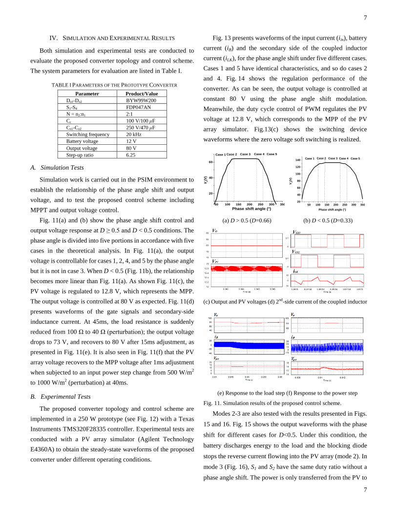
Both simulation and experimental tests are conducted to evaluate the proposed converter topology and control scheme. The system parameters for evaluation are listed in Table I.
TABLE I PARAMETERS OF THE PROTOTYPE CONVERTER
Parameter Product/Value Do1-Do2 BYW99W200 S1-S4 FDP047AN N = n2:n1 2:1 Cc 100 V/100 μF Co1-Co2 250 V/470 μF Switching frequency 20 kHz Battery voltage 12 V Output voltage 80 V Step-up ratio 6.25
A. Simulation Tests
Simulation work is carried out in the PSIM environment to establish the relationship of the phase angle shift and output voltage, and to test the proposed control scheme including MPPT and output voltage control.
Fig. 11(a) and (b) show the phase angle shift control and output voltage response at D ≥ 0.5 and D < 0.5 conditions. The phase angle is divided into five portions in accordance with five cases in the theoretical analysis. In Fig. 11(a), the output voltage is controllable for cases 1, 2, 4, and 5 by the phase angle but it is not in case 3. When D < 0.5 (Fig. 11b), the relationship becomes more linear than Fig. 11(a). As shown Fig. 11(c), the PV voltage is regulated to 12.8 V, which represents the MPP. The output voltage is controlled at 80 V as expected. Fig. 11(d) presents waveforms of the gate signals and secondary-side inductance current. At 45ms, the load resistance is suddenly reduced from 100 Ω to 40 Ω (perturbation); the output voltage drops to 73 V, and recovers to 80 V after 15ms adjustment, as presented in Fig. 11(e). It is also seen in Fig. 11(f) that the PV array voltage recovers to the MPP voltage after 1ms adjustment when subjected to an input power step change from 500 W/m2 to 1000 W/m2 (perturbation) at 40ms.
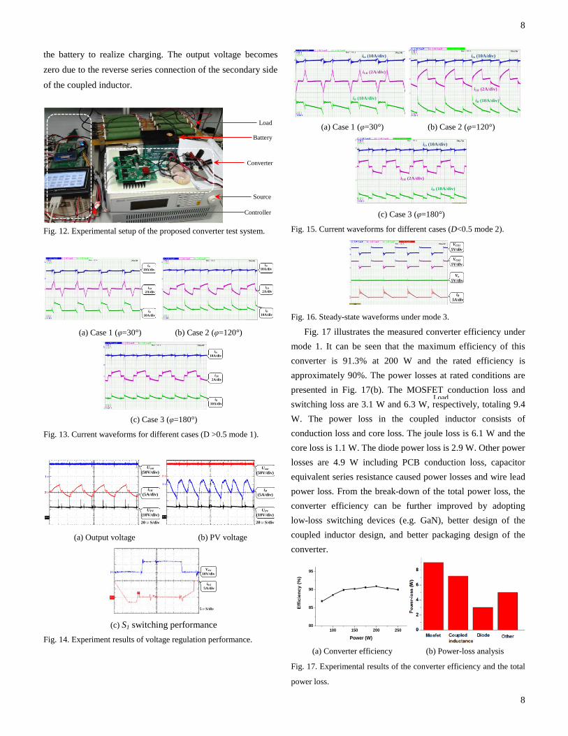
B. Experimental Tests
The proposed converter topology and control scheme are implemented in a 250 W prototype (see Fig. 12) with a Texas Instruments TMS320F28335 controller. Experimental tests are conducted with a PV array simulator (Agilent Technology E4360A) to obtain the steady-state waveforms of the proposed converter under different operating conditions.
Fig. 13 presents waveforms of the input current (iin), battery current (iB) and the secondary side of the coupled inductor current (iLK), for the phase angle shift under five different cases. Cases 1 and 5 have identical characteristics, and so do cases 2 and 4. Fig. 14 shows the regulation performance of the converter. As can be seen, the output voltage is controlled at constant 80 V using the phase angle shift modulation. Meanwhile, the duty cycle control of PWM regulates the PV voltage at 12.8 V, which corresponds to the MPP of the PV array simulator. Fig.13(c) shows the switching device waveforms where the zero voltage soft switching is realized.
(a) D > 0.5 (D=0.66) (b) D < 0.5 (D=0.33)
(c) Output and PV voltages (d) 2nd-side current of the coupled inductor
(e) Response to the load step (f) Response to the power step
Fig. 11. Simulation results of the proposed control scheme.
Modes 2-3 are also tested with the results presented in Figs. 15 and 16. Fig. 15 shows the output waveforms with the phase
shift for different cases for D<0.5. Under this condition, the battery discharges energy to the load and the blocking diode
stops the reverse current flowing into the PV array (mode 2). In mode 3 (Fig. 16), S1 and S2 have the same duty ratio without a
phase angle shift. The power is only transferred from the PV to
50 100 150 200 250 300 350
20
40
60
Case 5Case 4Case 3Case 2
Phase shift angle (°)V o(V
)
Case 1
50 100 150 200 250 300 35020
40
60
80
100
120
140 Case 5Case 3 Case 4Case 2
V o(V)
Phase shift angle (°)
Case 1
8
8
the battery to realize charging. The output voltage becomes zero due to the reverse series connection of the secondary side
of the coupled inductor.
Fig. 12. Experimental setup of the proposed converter test system.
(a) Case 1 (φ=30°) (b) Case 2 (φ=120°)
(c) Case 3 (φ=180°)
Fig. 13. Current waveforms for different cases (D >0.5 mode 1).
(a) Output voltage (b) PV voltage
Vds1 10V/div
ids1 5A/div
5μS/div (c) S1 switching performance
Fig. 14. Experiment results of voltage regulation performance.
(a) Case 1 (φ=30°) (b) Case 2 (φ=120°)
(c) Case 3 (φ=180°)
Fig. 15. Current waveforms for different cases (D<0.5 mode 2).
Fig. 16. Steady-state waveforms under mode 3.
Fig. 17 illustrates the measured converter efficiency under mode 1. It can be seen that the maximum efficiency of this converter is 91.3% at 200 W and the rated efficiency is approximately 90%. The power losses at rated conditions are presented in Fig. 17(b). The MOSFET conduction loss and switching loss are 3.1 W and 6.3 W, respectively, totaling 9.4 W. The power loss in the coupled inductor consists of conduction loss and core loss. The joule loss is 6.1 W and the core loss is 1.1 W. The diode power loss is 2.9 W. Other power losses are 4.9 W including PCB conduction loss, capacitor equivalent series resistance caused power losses and wire lead power loss. From the break-down of the total power loss, the converter efficiency can be further improved by adopting low-loss switching devices (e.g. GaN), better design of the coupled inductor design, and better packaging design of the converter.
(a) Converter efficiency (b) Power-loss analysis
Fig. 17. Experimental results of the converter efficiency and the total
power loss.
iin
10A/div
iLK 2A/div
iB 10A/div
iin
10A/div
iLK 2A/div
iB 10A/div
iin
10A/div
iLK 2A/div
iB 10A/div
20μS/div
iLK(5A/div)
UPV(10V/div)
Uout(50V/div)
20μS/div
iB(5A/div)
UPV(10V/div)
Uout(50V/div)
iin (10A/div)
iLK (2A/div)
iB (10A/div)
iin (10A/div)
iLK (2A/div)
iB (10A/div)
iin (10A/div)
iLK (2A/div)
iB (10A/div)
VGS15V/div
VGS25V/div
iB5A/div
Vo 5V/div
100 150 200 25080
85
90
95
Eff
icie
ncy
(%)
Power (W)
Load
Load
Battery
Converter
Source
Controller

9
9
V. CONCLUSIONS
This paper has presented an isolated three-port DC-DC converter for stand-alone PV systems, based on an improved Flyback-Forward topology. The converter can provide a high step-up capability for power conversion systems including the PV array, the battery storage, and the isolated load consumption. Three operating modes are analyzed and have shown the effective operation of the proposed topology for PV applications. From simulation and experimental tests, it can be seen that the output voltage and PV voltage can be controlled independently by the phase angle shift and PWM, respectively. The decoupled control approach is a simple but effective way to achieve the regulation of output voltage and PV voltage, which is important for MPPT of stand-alone PV systems. In addition, a 250 W converter is prototyped and tested to verify the effectiveness of the proposed converter topology and control scheme.
The developed technology is capable of achieving MPPT, high conversion ratio and multiple operating modes whist still making the converter relatively simple, light, efficient and cost-effective.
REFERENCES
[1] K. Basu, N. Mohan, “A high-frequency link single-stage PWM inverter with common-mode voltage suppression and source-based commutation of leakage energy,” IEEE Trans. Power Electron., vol. 28, no. 8, pp. 3907-3918, Oct. 2014.
[2] C. Konstantopoulos, E. Koutroulis, “Global maximum power point tracking of flexible photovoltaic modules,” IEEE Trans. Power Electron., vol. 29, no. 6, pp. 2817-2828, Oct. 2014.
[3] W. Li, W. Li, X. Xiang, Y. Hu, X. He, “High step-up interleaved converter with built-in transformer voltage multiplier cells for sustainable energy applications,” IEEE Trans. Power Electron., vol. 29, no. 6, pp. 2829-2836, Jun. 2014.
[4] Y. Hu, Y. Deng, Q. Liu, X. He, “Asymmetry three-level grid-connected current hysteresis control with varying bus voltage and virtual over-sample method,” IEEE Trans. Power Electron. vol. 29, no. 6, pp. 3214-3222, Jun. 2014.
[5] F. Nejabatkhah, S. Danyali, S. H. Hosseini, M. Sabahi,and S. M. Niapour, “Modeling and control of a new three-input DC-DC boost converter for hybrid PV/FC/battery power system,” IEEE Trans. Power Electron., vol. 28, no. 10, pp. 4612-4624, Oct. 2013.
[6] F. Zhang, K. Thanapalan, A. Procter, S. Carr, J. Maddy, “Adaptive Hybrid Maximum Power Point Tracking Method for a Photovoltaic System,” IEEE Trans. Energy Conversion, vol. 28, no. 2, pp. 353-360, June 2013.
[7] P. Thounthong, “Model Based-Energy Control of a Solar Power Plant With a Supercapacitor for Grid-Independent Applications,” IEEE Trans. Energy Conversion, vol. 26, no. 4, pp. 1210-1218, 2011.
[8] A. Elmitwally, M. Rashed, “Flexible Operation Strategy for an Isolated PV-Diesel Microgrid Without Energy Storage,” IEEE Trans. Energy Conversion, vol. 26, no. 1, pp. 235-244, 2011.
[9] J. K. Shiau, D. M. Ma, P. Y. Yang, G. F. Wang, and J. H. Gong, “Design of a Solar Power Management System for an Experimental UAV,” IEEE Trans. Aerospace and Electronic Systems, vol. 45, no. 4, pp. 1350-1360, Oct. 2009.
[10] F. S. Kang, S. J. Park, S. E. Cho, C. U. Kim, T. Ise, “Multilevel PWM inverters suitable for the use of stand-alone photovoltaic power systems,” IEEE Trans. Energy Conversion, vol. 20, no. 4 , pp. 906-915, 2005.
[11] H. Valderrama-Blavi, J. M. Bosque, F. Guinjoan, L. Marroyo, and L. Martinez-Salamero, “Power Adaptor Device for Domestic DC Microgrids Based on Commercial MPPT Inverters,” IEEE Trans. Ind. Electron., vol. 60, no. 3, pp. 1191-1203, Mar. 2013.
[12] H. Wu, K. Sun, R. Chen, H. Hu, and Y. Xing, “Full-Bridge Three-Port Converters With Wide Input Voltage Range for Renewable Power Systems,” IEEE Trans. Power Electron., vol. 27, no. 9, pp. 3965-3974, Sept. 2012.
[13] O. Elma, and U. S. Selamogullari, “A comparative sizing analysis of a renewable energy supplied stand-alone house considering both demand side and source side dynamics,” Applied Energy, vol. 96, pp. 400-408, 2012.
[14] H. Wu, R. Chen, J. Zhang, Y. Xing, H. Hu, and H. Ge, “A Family of Three-Port Half-Bridge Converters for a Stand-Alone Renewable Power System,” IEEE Trans. Power Electron., vol. 26, no. 9, pp. 2697-2706, Sept. 2011.
[15] Z. Qian, O. Abdel-Rahman, and I. Batarseh, “An Integrated Four-Port DC/DC Converter for Renewable Energy Applications,” IEEE Trans. Power Electron., vol. 25, no. 7, pp. 1877-1887, July 2010.
[16] E. Sanchis, E. Maset, A. Ferreres, J. B. Ejea, V. Esteve, J. Jordan, J. Calvente, A. Garrigos, and J. M. Blanes, “Bidirectional High-Efficiency Nonisolated Step-Up Battery Regulator,” IEEE Trans. Aerospace and Electronic Systems, vol. 47, no. 3, pp. 2230-2239, Jul. 2011.
[17] K. Shenai, P. G. Neudeck, and G. Schwarze, “Design and technology of compact high-power converters,” IEEE Aerospace and Electronic Systems Magazine, vol. 16, no. 3, pp. 27-31, Aug. 2001.
[18] S. Kim, H.-S. Song, and K. Nam, “Idling Port Isolation Control of Three-Port Bidirectional Converter for EVs,” IEEE Trans. Power Electron., vol. 27, no. 5, pp. 2495-2506, May 2012.
[19] C. Zhao, S. D. Round, and J. W. Kolar, “An Isolated Three-Port Bidirectional DC-DC Converter With Decoupled Power Flow Management,” IEEE Trans.Power Electrons., vol. 23, no. 5, pp. 2443-2453, Sept. 2008.
[20] H. Tao, J. L. Duarte, and M. A. M. Hendrix, “Three-Port Triple-Half-Bridge Bidirectional Converter With Zero-Voltage Switching,” IEEE Trans. Power Electron., vol. 23, no. 2, pp. 782-792, Mar. 2008.
[21] J. L. Duarte, M. Hendrix, and M. G. Simoes, “Three-Port Bidirectional Converter for Hybrid Fuel Cell Systems,” IEEE Trans. Power Electron., vol. 22, no. 2, pp. 480-487, Mar. 2007.
[22] H. Wu, P. Xu, H. Hu, Z. Zhou, and Y. Xing, “Multi-port Converters Based on Integration of Full-Bridge and Bidirectional DC-DC Topologies for Renewable Generation Systems,” IEEE Trans. Ind. Electron., vol. PP, no. 99, pp. 1-1, in press, 2013.
[23] Z. Ouyang, Z. Zhang, M. A. E. Andersen, and O. C. Thomsen, “Four Quadrants Integrated Transformers for Dual-Input Isolated DC-DC Converters,” IEEE Trans. Power Electron., vol. 27, no. 6, pp. 2697-2702, June 2012.
[24] L. Wang, Z. Wang, and H. Li, “Asymmetrical Duty Cycle Control and Decoupled Power Flow Design of a Three-port Bidirectional DC-DC Converter for Fuel Cell Vehicle Application,” IEEE Trans. Power Electron., vol. 27, no. 2, pp. 891-904, Feb. 2012.
[25] R. J. Wai, C. Y. Lin, and Y. R. Chang, “High Step-Up Bidirectional Isolated Converter With Two Input Power Sources,” IEEE Trans. Ind. Electron., vol. 56, no. 7, pp. 2629-2643, July 2009.
[26] W. Li, L. Fan, Y. Zhao, X. He, D. Xu, and B. Wu, “High-Step-Up and High-Efficiency Fuel-Cell Power-Generation System With Active-Clamp Flyback-Forward Converter,” IEEE Trans. Ind. Electron., vol. 59, no. 1, pp. 599-610, 2012.
[27] Z. Qian, O. Abdel-Rahman, H. Al-Atrash, and I. Batarseh, “Modeling and Control of Three-Port DC/DC Converter Interface for Satellite Applications,” IEEE Trans. Power Electron., vol. 25, no. 3, pp. 637-649, 2010.
[28] P. Bajpai, and V. Dash, “Hybrid renewable energy systems for power generation in stand-alone applications: A review,” Renewable and Sustainable Energy Reviews, vol. 16, no. 5, pp. 2926-2939, 2012.

10
10
[29] H. Tao, A. Kotsopoulos, J. L. Duarte, and M. A. M. Hendrix, “Family of multiport bidirectional DC-DC converters,” IEE Proc. Electric Power Applications, vol. 153, no. 3, pp. 451-458, May 2006.
[30] B. G. Dobbs, and P. L. Chapman, “A multiple-input DC-DC converter topology,” IEEE Power Electronics Letters, vol. 1, no. 1, pp. 6-9, Mar. 2003.
[31] Z. Wang, and H. Li, “An Integrated Three-Port Bidirectional DC-DC Converter for PV Application on a DC Distribution System,” IEEE Trans. Power Electron., vol. 28, no. 10, pp. 4612-4624, Oct. 2013.
[32] W. Cai, B. Liu, S. Duan, L. Jiang, “Power flow control and optimization of a three-port converter for photovoltaic-storage hybrid system,” Energy Conversion Congress and Exposition (ECCE), pp. 4121-4128, 2012.
[33] Y. M. Chen, X. Yu, A. Q. Huang, “A new nonisolated three-port DC-DC converter with high step-up/down ratio,” the 2012 IEEE Energy Conversion Congress and Exposition (ECCE), pp. 1520-1526, 2012.
[34] Q. Wang, J. Zhang, X. Ruan, and K. Jin, “Isolated Single Primary Winding Multiple-Input Converters,” IEEE Trans. Power Electron., vol. 26, no. 12, pp. 3435-3442, Dec. 2011.
[35] Y. Li, X. Ruan, D. Yang, F. Liu, and C. K. Tse, “Synthesis of Multiple-Input DC/DC Converters,” IEEE Trans. Power Electron., vol. 25, no. 9, pp. 2372-2385, Sept. 2010.
[36] H. Krishnaswami, and N. Mohan, “Three-Port Series-Resonant DC-DC Converter to Interface Renewable Energy Sources With Bidirectional Load and Energy Storage Ports,” IEEE Trans. Power Electron., vol. 24, no. 10, pp. 2289-2297, Oct. 2009.
[37] H. Tao, A. Kotsopoulos, J. L. Duarte, and M. A. M. Hendrix, “Transformer-Coupled Multiport ZVS Bidirectional DC-DC Converter With Wide Input Range,” IEEE Trans. Power Electron., vol. 23, no. 2, pp. 771-781, Mar. 2008.
[38] W. Li, J. Xiao, Y. Zhao, and X. He, “PWM Plus Phase Angle Shift (PPAS) Control Scheme for Combined Multiport DC/DC Converters,” IEEE Trans. Power Electron., vol. 27, no. 3, pp. 1479-1489, 2012.
[39] Yihua Hu, Yan Deng, Jiangtao Long, Xiaoxun Lu, Xiangning He. “A Three-port High Step-up DC-DC Converter for PV System,” ECCE-Asia, Australia, 2013.
[40] W. Xiao, A. Elnosh, V. Khadkikar, and H. Zeineldin, “Overview of maximum power point tracking technologies for photovoltaic power systems,” in Proc. Annual Conference on IEEE Industrial Electronics Society, 2011, pp. 3900-3905.
[41] W. Xiao, W. G. Dunford, P. R. Palmer, and A. Capel, “Regulation of Photovoltaic Voltage,” IEEE Trans. Industrial Electronics, vol. 54, no. 3, pp. 1365-1374, Jun. 2007.
Yihua Hu (M’13) received the B.S. degree in electrical motor drives in 2003, and the Ph.D. degree in power electronics and drives in 2011, both from China University of Mining and Technology, Jiangsu, China. Between 2011 and 2013, he was with the College of Electrical Engineering, Zhejiang University as a Postdoctoral Fellow. Between November 2012 and February 2013, he was an academic Visiting Scholar with the School of
Electrical and Electronic Engineering, Newcastle University, Newcastle upon Tyne, UK. He is currently a Research Associate with the Department of Electronic & Electrical Engineering, University of Strathclyde, Glasgow, UK. He has published more than 20 technical papers in leading journals and conference proceedings. His research interests include PV generation systems, DC-DC/DC-AC converters, and electrical motor drives.
Weidong Xiao (S’04-M’07-SM’13) received the Master degree and the Ph.D. degree from the University of British Columbia, Vancouver, Canada, in 2003 and 2007 respectively. He is an associate professor working with the department of electrical engineering and computer science (EECS) at the Masdar Institute of Science and Technology, Abu Dhabi, UAE. In 2010, he was a visiting scholar with
the Massachusetts Institute of Technology (MIT) Cambridge, USA, where he worked on the power interfaces for PV power systems. Prior to the academic career, Dr. Xiao worked with the MSR Innovations Inc. in Canada as a R&D engineering manager focusing on integration, research, optimization and design of photovoltaic power systems. Dr. Xiao serves as the guest editor for the IEEE Transactions on Industrial Electronics Special Edition on photovoltaic power systems. His research interest includes photovoltaic power systems, power electronics, dynamic systems and control, and industry applications.
Wenping Cao (M’05-SM’11) (correspondence author) received the B.Eng in electrical engineering from Beijing Jiaotong University, Beijing, China, in 1991; and the Ph.D. degree in electrical machines and drives from the University of Nottingham, Nottingham, U.K., in 2004. He is currently a Senior Lecturer with Queen’s University Belfast, Belfast, U.K. He is the recipient of the Best Paper Award at the LDIA’13 Conference. Dr. Cao serves as an Associate Editor for IEEE Transactions on Industry Applications, IEEE Industry Applications Magazine,
IET Power Electronics, and nine other International Journals. His research interests are in thermal performance of electric machines, drives and power electronics. Dr. Cao is also a Member of the Institution of Engineering and Technology (IET) and a Fellow of Higher Education Academy (HEA).
Bing Ji (M’13) received the M.Sc. and Ph.D. degrees in electrical and electronic engineering from Newcastle University, England, in 2007 and 2012, respectively. He was a power electronics engineer with a UK low-emission vehicle company from 2012, where he worked on powertrain development for hybrid electric vehicles and battery management systems. Since 2013, he has been a Postdoctoral Researcher at Newcastle University, where he is involved in accurate power loss measurement and
health management for power electronics. His research interests include reliability study of power semiconductor devices, batteries and power electronics converters, function integration of gate drivers, electro-thermal modelng, thermal management and high power-density converter integration for electric vehicle applications. He is also a member of the IET.
D. John Morrow (M’99) received the B.Sc and Ph.D. degrees from Queen’s University Belfast, Belfast, U.K., in 1982 and 1987, respectively. Since 1987, he has been a Lecturer in electrical engineering at Queen’s University Belfast, Belfast, U.K., with research interests in electric power systems, power system instrumentation, and embedded generation. Dr. Morrow is a member of the IET and also a member of the IEEE PES Excitation Systems Subcommittee.