three-dimensional packaging for wide bandgap based ... · group leader . [email protected]. brice...
TRANSCRIPT

535 W. Research Center Blvd. • Fayetteville, AR 72701 • (479) 443-5759
Three-Dimensional Packaging for Wide Bandgap Based Discrete and Multi-Chip Power Packages
www.apei.net
Brandon Passmore Sr. Electronics Packaging Research Engineer and Packaging Group Leader [email protected] Brice McPherson, Zach Cole, Peter Killeen, Bret Whitaker, Dan Martin, Adam Barkley, Ty McNutt, Kraig Olejniczak, and Alex Lostetter Applied Power Electronics Conference and Exposition (APEC), March 16 – 20, 2014

www.apei.net
Outline
2
• Company Overview • Motivation of 3D packaging
techniques with wide bandgap power electronics
• Design and performance of X-5 multi-chip power module
• Design and performance of X-6 discrete package
• Summary

www.apei.net
APEI, Inc. Core Technologies
3
Multi-Chip Packaging
High Reliability Modules
Power Circuits & Systems
SiC & GaN Device Expertise
High Density, High Performance Power Electronics
Find us at:

www.apei.net
Motivation for Wide Bandgap Power Electronics
4
High Temperature
Operation
Enabling Capability
High Power Density
Fast Switching;
High Frequency
• Reduce cooling requirements • Reduce system volume/weight • Reduce complexity • Improve performance /reliability
Key Benefits
• High current density • High thermal conductivity substrate
• Reduce size of power filters/capacitors • Reduce size/weight of power system • Allows higher bandwidth for control loops reducing error in AC systems
High temperature multi-layer technologies reduce package size and
increase reliability
3D Packaging Technologies
High current wire bondless
interconnections
Multi-layer packaging technologies reduce
parasitics
www.apei.net
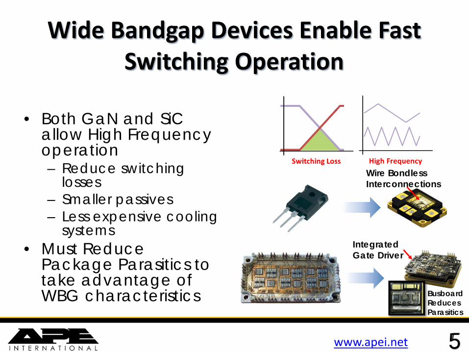
Wide Bandgap Devices Enable Fast Switching Operation
5
• Both GaN and SiC allow High Frequency operation – Reduce switching
losses – Smaller passives – Less expensive cooling
systems • Must Reduce
Package Parasitics to take advantage of WBG characteristics
Integrated Gate Driver
Busboard Reduces Parasitics
Wire Bondless Interconnections


www.apei.net
Design of X-5 Power Module with Integrated Gate Driver
7
Specifications • Full-bridge configuration • 50+ A / 1200 V • 225 °C maximum operation (Tjmax) • 2 MOSFETs / 1 Schottky diode per
switch position • 58 mm × 41 mm × 13 mm (1/3 the
volume of a deck of cards) Package Components • Metal-matrix composite baseplate • AlN DBC Power substrate • High temperature die and power
substrate attach • Integrated busboard enables 3D
Packaging • Integrated gate driver
58 mm
13 mm 41 mm

www.apei.net
X-5 SiC MCPM Junction to Case Thermal Resistance
8
• Experiment ∆Tj-c = 17 °C and Model ∆Tj-c = 15 °C • The experimental and modeled ∆Tj-c are in good agreement • A low junction-to-case thermal resistance of 0.18 °C/W was
measured Experiment Model
Total Pdis = 95.5 W
Spot 136 °C

www.apei.net
0123456
1.E+02 1.E+03 1.E+04 1.E+05 1.E+06
Resi
stan
ce (m
Ω)
Frequency (Hz)
Power Loop Resistance
14
16
18
20
22
1.E+02 1.E+03 1.E+04 1.E+05 1.E+06
Indu
ctan
ce (n
H)
Frequency (Hz)
Power Loop Inductance
Low Parasitic Power Module for High Speed Switching
9
• 3D parasitic model using Comsol Multiphysics® • One side of the full-bridge was analyzed due to the
symmetric design • Inductance/Resistance was modeled vs. frequency
up to 1 MHz • The X-5 exhibited low parasitics at high frequencies • ~4 mΩ and ~16 nH at 500 kHz • Inductance is roughly 1/2 of other commercial power
brick style module [1]
500 kHz
500 kHz
[1] http://www.semikron.com/products/data/cur/assets/SKM100GB12T4_22892020.pdf

www.apei.net
Ultra-Fast Switching From Low Parasitic X-5 / Gate Driver Integration
10
Turn On Waveform
Gate Voltage
Drain Voltage
7.5 ns
• Clamped inductive load • 400 V / 30 A switching waveforms • Rise time = 16.1 ns • Fall time = 7.5 ns • Switching Frequency = 1.2 MHz • Minimal ringing and overshoot
92%
94%
96%
98%
100%
1000 2000 3000 4000 5000 6000
Effic
ienc
y
Output Power [W]
fsw = 250 kHzfsw = 500 kHzfsw = 1 MHzfsw = 1.2 MHz
Boost Converter Efficiency vs. Power

www.apei.net
SiC Charger for Next Generation Toyota Prius Plug-in Hybrid
11
88%
90%
92%
94%
96%
1000 2000 3000 4000 5000 6000
Effic
ienc
y
Output Power
System Efficiency vs. Output Power
System with AC-DC @ 500 kHz
System with AC-DC @ 250 kHz
[2] Toyota, "Plug-in hybrid 2010 model revised (includes 2012 model) emergency response guide," 22 Feb. 2012.
[3] Department of Energy, "EV everywhere: a grand challenge in plug-in electric vehicles, “ 2012.
CHARGER SYSTEM DESIGN TARGETS
Funded by DOE ARPA-e Program
Specifications 2010 Toyota Prius PHEV Charger [2]
Preliminary DOE PHEV On-Board Charger
Targets for 2022 [3]
APEI, Inc. Prototype SiC PHEV Charger
Power Level 2.9 kW 3.3 kW 6.1 kW (Peak) Volume 6.4 L 3.5 L 1.2 L Mass 6.6 kg 3.5 kg 1.6 kg Volumetric power density 0.45 kW/L 0.943 kW/L 5.0 kW/L Gravimetric power density 0.42 kW/kg 0.943 kW/kg 3.8 kW/kg Efficiency 94% >95%
> 10× Power Density
Battery Charger
X-5 Power Module

www.apei.net
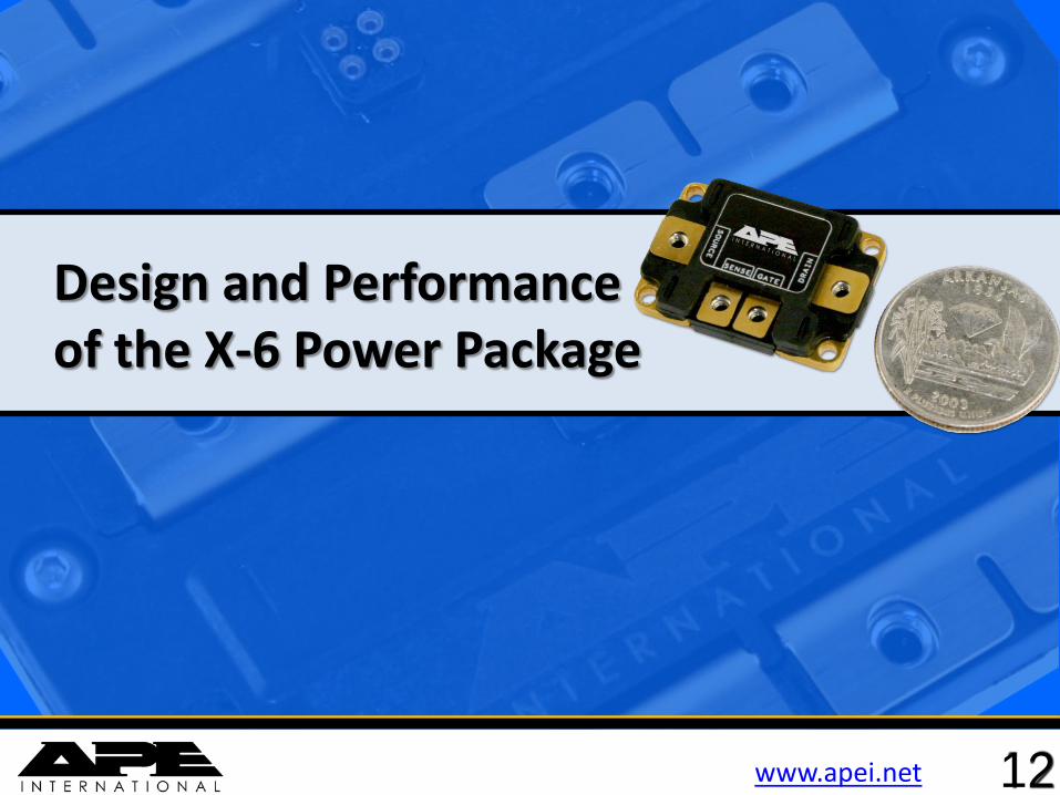
Design of X-6 Power Package
13
Specifications • Single die and co-pack • 100+ A / 1200 V • 225 °C maximum operation (Tjmax) • 30 mm × 21 mm × 7 mm Package Features • Compatible with SiC and GaN • Electrically Isolated AlN DBC power substrate • High temperature die and power substrate
attach • High current capable • Low inductance (< 8 nH) • Ultra-fast switching (< 4 ns) • Low Rjc
– 2 mm × 2 mm Die 1.23 °C/W – 5 mm × 5 mm Die 0.5 °C/W
• Modular for system integration • Wire bonded or bondless versions
Wire Bondless Package
Wire Bonded Package
SiC MOSFET X-6 Package

www.apei.net
Wirebondless X-6 Assembly
14
This image cannot currently be displayed.
Housing High temperature plastic) Injection molded
Fasteners Low profile “Captive” in plastic
Interconnects *For wire bondless configurations
PCB, DBC, Thick Film
Contacts
Base Plate
Substrate
Panelized & Etched
DBC, DBA, AMB, etc.
Copper or MMC


www.apei.net
X-6 Package Junction to Case Thermal Resistance
16
• Experimental Rj-c = 1.23 °C/W • Modeled Rj-c = 1.15 °C/W • The experimental and modeled
Rj-c are in good agreement • ~ 50 % of the thermal
resistance of the package is in the AlN layer of the DBC
• Rj-c can be reduced further using DBC with a thinner AlN layer
Experiment
Model
Pdis = 48 W
Pdis = 48 W
Spot = 66 °C

www.apei.net
X-6 Parasitic Modeling
17
FLIP CHIP Dual Substrate
WIRE BOND LOOPS WIRE BOND LOOPS
X-6 Package TO-254 Package
PIN LENGTH
Wire Bonded SiC TMOS Wire Bondless GaN HEMT TO-254 – SiC TMOS

www.apei.net
Discrete Package Resistance Comparison
18
GaN HEMT SiC TMOS TO-254 0 >4
A/mm2
Current Density
Power Loop
0 >4 A/mm2
Current Density
Gate Loop

www.apei.net
Discrete Package Inductance Comparison
19
GaN HEMT SiC TMOS TO-254
Wire Bonded SiC TMOS
Wire Bondless GaN HEMT
TO-254 – SiC TMOS

www.apei.net
High Efficiency GaN HEMT Boost Convertor
20
• 200 - 300 V Input / 400 V Output • Switching Frequency = 100 kHz • Turn on ~ 8.2 ns, Turn off ~ 3.7 ns • Minimal Ringing • Up to 5 kW • > 99 % Peak Efficiency @ 100 kHz • 97.5 % @ 1 MHz
3.72 ns

www.apei.net
Summary
21
• Wide bandgap power packages using 3D packaging technologies were presented
• The electrical and thermal characteristics of the X-5 and X-6 were introduced
• The SiC-based X-5 demonstrated > 95% efficiency and a 5 kW/L volumetric power density in next generation Toyota Prius charger
• The GaN-based X-6 exhibited ultra-fast switching (< 4 ns) and a high efficiency (> 99 %) in a boost configuration
APEI’s X-5 Power Module
APEI’s X-6 Power Package

www.apei.net
Connect With Us!
22
• Half-bridge +300 A / 1200 V • Standard power module footprint • Device neutral • 225 °C maximum operation (Tjmax) • Minimized parasitics (< 7 nH) • Low thermal resistance (< 0.1 °C/W) • Low volume/weight (72 cm3 and 140 g)
Wide Bandgap HT-3000 Power Module