thin films spin coating epitaxial films...thin films spin coating epitaxial films meagan v. kelso 1,...
TRANSCRIPT
THIN FILMS
Spin coating epitaxial filmsMeagan V. Kelso1, Naveen K. Mahenderkar1*, Qingzhi Chen2,John Z. Tubbesing2, Jay A. Switzer,2†
Spin-coated films, such as photoresists for lithography or perovskite films forsolar cells, are either amorphous or polycrystalline. We show that epitaxial films ofinorganic materials such as cesium lead bromide (CsPbBr3), lead(II) iodide (PbI2),zinc oxide (ZnO), and sodium chloride (NaCl) can be deposited onto a variety ofsingle-crystal and single-crystal–like substrates by simply spin coating either solutionsof the material or precursors to the material. The out-of-plane and in-plane orientationsof the spin-coated films are determined by the substrate. The thin stagnant layerof supersaturated solution produced during spin coating promotes heterogeneousnucleation of the material onto the single-crystal substrate over homogeneousnucleation in the bulk solution, and ordered anion adlayers may lower the activationenergy for nucleation on the surface. The method can be used to produce functionalmaterials such as inorganic semiconductors or to deposit water-soluble materialssuch as NaCl that can serve as growth templates.
Epitaxy is the growth of crystals whose orien-tation is determined by their crystalline sub-strate (1, 2). Epitaxy can produce thin filmswith atomic perfection that rivals that ofsingle crystals as well asmetastable phases
(such as body-centered cubic Ni on Fe and face-centered cubic Fe onCu), superlattices, quantumwells, and strained-layer architectures with tun-able properties (2). Although epitaxial growth isusually constrained to ultrahigh vacuum or hightemperatures by techniques such as molecularbeam epitaxy, chemical vapor deposition, andliquid-phase epitaxy, it was first demonstratedin aqueous solution in 1836 when Frankenheimshowed that sodium nitrate crystals could begrown epitaxially on a freshly cleaved calcitesubstrate (3). In 1950, Johnson also used aque-ous solution to growNaCl crystals epitaxially onsingle-crystal Ag (4). Other examples of solution-based deposition of epitaxial films are hydro-thermal processing (5), chemical bath deposition(6–8), and electrodeposition (9–11).Each of these solutionmethods has limitations.
Hydrothermal processing requires high tempera-ture and pressure, chemical bath deposition re-quires specific reactions to occur at the substratesurface, and electrodeposition requires conduct-ing or semiconducting substrates. Here, we showthat epitaxial films can be deposited by a simple,rapid, and inexpensive spin-coating method di-rectly from solution precursors.Wedemonstratethe epitaxial growth of a diverse array of inor-ganic materials such as CsPbBr3, PbI2, NaCl, andZnO onto a variety of single-crystal and single-crystal–like substrates such as Au, Ag, SrTiO3,
andmica by spin coating with low-temperaturein situ heating.Spin coating is used commercially to deposit
polymer films for lithography. It has also beenused to deposit organic semiconductor films(12, 13) and has become the preferred deposi-
tion method for perovskite materials such asCH3NH3PbI3 and CsPbBr3 for use in solar cells,photodetectors, and light-emitting diodes (LEDs)(14–19). For example, dense and uniform films ofCH3NH3PbI3−xBrxhave been spin coated by engi-neering the solventmix (17), andCH3NH3PbI3−xClxfilms with millimeter-scale crystal grains havebeen spin coated by dispensing the precursorsolution onto a heated substrate (16). However,the substrates in this earlier work were poly-crystalline or amorphous, so the films were notepitaxial. Ji et al. have spin coated CH3NH3PbI3onto single-crystal KCl and crystallized the as-deposited amorphous material into an epitaxialfilm with a final annealing step (19). There hasalso been previous work on the spin coating ofamorphous sol-gel precursors for oxides ontosingle-crystal surfaces that were then convertedinto epitaxial films by a high-temperature burnoff of organics (20–22). In the present work,the epitaxial films were directly spin coatedfrom solution precursors without the need forpostannealing or a high-temperature conver-sion step.We propose that the very thin supersaturated
solution layer that is formed in spin coating servesto promote heterogeneous nucleation of thematerial onto the single-crystal substrate overhomogeneous nucleation in the bulk solution
RESEARCH
Kelso et al., Science 364, 166–169 (2019) 12 April 2019 1 of 4
1Department of Materials Science and Engineering andGraduate Center for Materials Research, Missouri Universityof Science and Technology, Rolla, MO 65409-1170, USA.2Department of Chemistry and Graduate Center for MaterialsResearch, Missouri University of Science and Technology,Rolla, MO 65409-1170, USA.*Present address: Lam Research Corporation, 4650 CushingParkway, Fremont, CA 94538, USA.†Corresponding author. Email: [email protected]
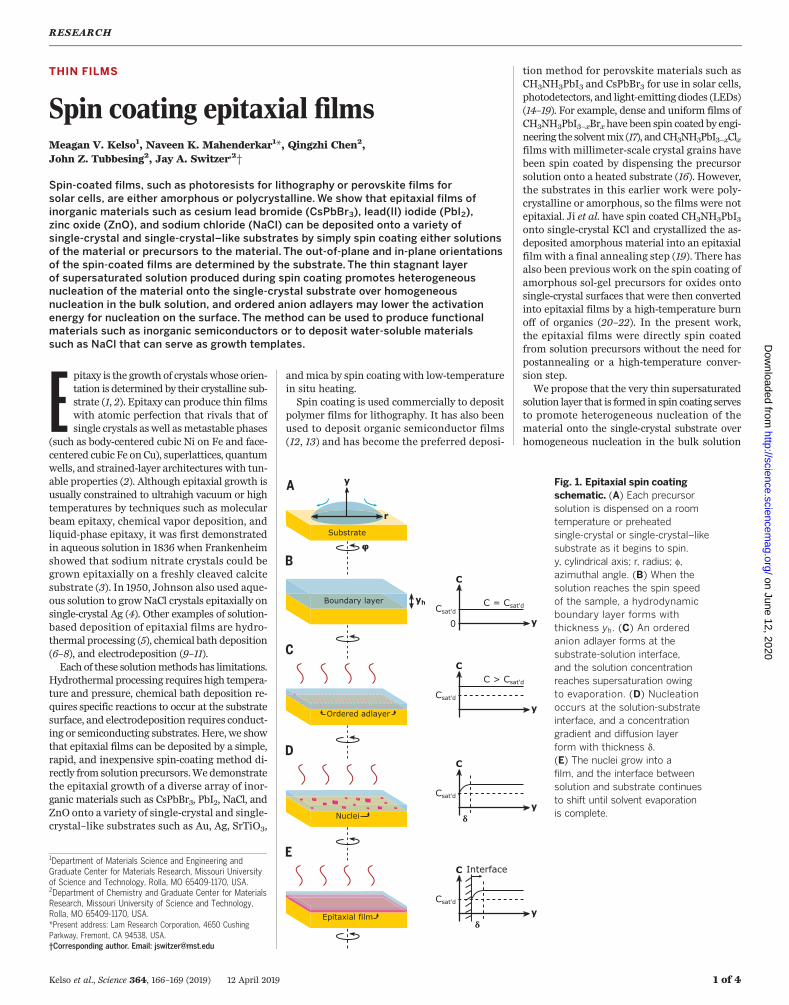
Fig. 1. Epitaxial spin coatingschematic. (A) Each precursorsolution is dispensed on a roomtemperature or preheatedsingle-crystal or single-crystal–likesubstrate as it begins to spin.y, cylindrical axis; r, radius; f,azimuthal angle. (B) When thesolution reaches the spin speedof the sample, a hydrodynamicboundary layer forms withthickness yh. (C) An orderedanion adlayer forms at thesubstrate-solution interface,and the solution concentrationreaches supersaturation owingto evaporation. (D) Nucleationoccurs at the solution-substrateinterface, and a concentrationgradient and diffusion layerform with thickness d.(E) The nuclei grow into afilm, and the interface betweensolution and substrate continuesto shift until solvent evaporationis complete.
on June 12, 2020
http://science.sciencemag.org/
Dow
nloaded from
that would occur during crystallization by con-ventional solvent evaporation methods. Theactivation energy for nucleation on the single-crystal surface may also be lowered by theproduction of ordered adlayers of anions onthe surface. Anions specifically adsorb on single-crystal metal surfaces to form monolayer orsubmonolayer adlayers (23). For example, I−
forms a (√3 by √3)R30° adlayer on Au(111),and Cl− forms a c(2 by 2) adlayer on Ag(100).These anion adlayers could mimic the anion-terminated surfaces of compounds to serve asseed crystals for the nucleation of the spin-coatedmaterial.The general mechanism for epitaxial spin
coating that we outline in Fig. 1 assumes that theformation of a hydrodynamic boundary layerand the subsequent evaporation of the solventoccur in steps, as opposed to more rigorousmodels in which the two processes occur simulta-neously (24, 25). A drop of solution containingdissolved material or precursors is dispensedonto the rotating substrate (Fig. 1A). After spinning,the solution forms a stagnant hydrodynamicboundary layer (Fig. 1B) whose thickness, yh , isdetermined by the kinematic viscosity, v, of thesolution and the rotation rate, w (in terms ofangular frequency of rotation, measured in s−1),of the substrate (26):
yh ¼ 3:6v
w
� �1=2ð1Þ
For example, a rotation rate of 3000 rpm and akinematic viscosity of 0.01 cm2 s−1 will generate
a boundary layer ~200 mm thick. An orderedadlayer that lowers the activation energy fornucleation also forms at this stage (Fig. 1C).Because of the in situ heating and the spinningof the substrate, the solvent evaporates and thesolution reaches supersaturation (Fig. 1C). Oncethe supersaturation reaches the critical value fornucleation, the nuclei formon the substrate, andthe concentration at the solid-liquid interface isreduced to the saturation concentration of thesolution, csat’d. A concentration gradient is thenestablished that serves as the driving force forthe ion or molecule diffusion (Fig. 1D). The dif-fusion layer thickness, d, is given by Eq. 2, whereD is the diffusion coefficient of dissolved species(cm2 s−1) (26):
d ¼ 1:61D1=3w�1=2v1=6 ð2Þ
For a rotation rate of 3000 rpm and a diffusioncoefficient of 1 × 10⁻⁶ cm2 s−1, the diffusion layerwould be ~4 mmthick. An epitaxial film continuesto grow until the solvent completely evaporates(Fig. 1E). A similar model is observed in chem-ical vapor deposition and liquid phase epitaxy,in which film growth occurs by mass transportacross a diffusion layer (1).The spin coating of epitaxial films requires
either that the material to be spin coated is sol-uble or that a soluble precursor to the material isavailable that can be converted to the materialafter drying at slightly increased temperatures.For the first case, we have spin coated PbI2 fromN,N-dimethylformamide (DMF) solution, CsPbBr3from dimethyl sulfoxide (DMSO) solution, and
NaCl from aqueous solution. For the second case,we have spin coated ZnO from an aqueous am-monia solution of Zn(II) (27). In the ZnO case,the NH3 evolved during the spin-coating process.The concentrations and conditions for spin coat-ing are given in the supplementary materials.The substrates used for spin coating were eithersingle crystals such as SrTiO3 andmica or proxiesfor single crystals that were thin epitaxial filmsof Au or Ag that were electrodeposited ontosingle-crystal Si wafers (11, 28, 29). PbI2, CsPbBr3,and ZnO are all functional materials that canserve as semiconductors in solar cells and LEDs(9, 15, 27, 30). Epitaxial NaCl can serve as awater-soluble template for large-scale epitaxial lift-offof flexible single-crystal–like materials for elec-tronics, solar cells, and displays (31).The in-plane order of the spin-coated mate-
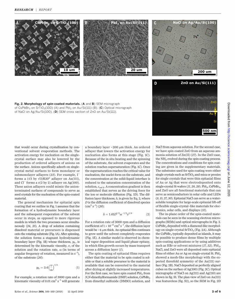
rials can be seen in the scanning electronmicro-graphs (SEMs) and opticalmicrographs in Fig. 2.CsPbBr3 depositedwith a diamond-likemorphol-ogy on single-crystal SrTiO3 (Fig. 2A). Althoughthe CsPbBr3 typically deposited as islands, it maybe possible to produce dense films by multiplespin-coating applications or by using additivessuch as HBr or solvent mixtures (17, 32). PbI2,NaCl, and ZnOwere all deposited onto epitaxialfilms of either Au or Ag on single-crystal Si. PbI2showed a mesh-like morphology with the ex-pected threefold symmetry of the Au(111) sur-face (Fig. 2B). NaCl deposited as perfectly alignedcubes on the surface of Ag(100) (Fig. 2C). Opticalmicrographs of NaCl on Ag(111) and Ag(110) areshown in fig. S1. The plan view of ZnO on Au(111)was featureless (fig. S2), so the SEM in Fig. 2D
Kelso et al., Science 364, 166–169 (2019) 12 April 2019 2 of 4
Fig. 2. Morphology of spin-coated materials. (A and B) SEM micrographof CsPbBr3 on SrTiO3(100) (A) and PbI2 on Au/Si(111) (B). (C) Optical micrographof NaCl on Ag/Au/Si(100). (D) SEM cross section of ZnO on Au/Si(111).
RESEARCH | REPORTon June 12, 2020
http://science.sciencemag.org/
Dow
nloaded from
is a cross-sectional view of the ~500-nm-thickZnO film.The crystallographic orientation of the spin-
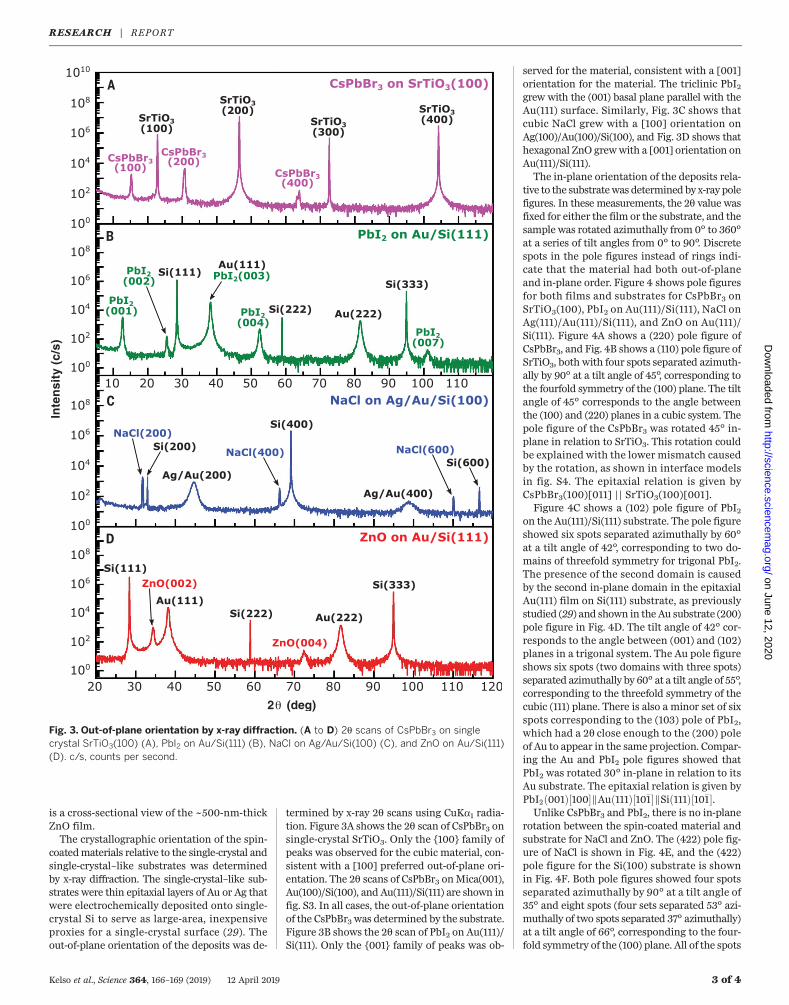
coatedmaterials relative to the single-crystal andsingle-crystal–like substrates was determinedby x-ray diffraction. The single-crystal–like sub-strates were thin epitaxial layers of Au or Ag thatwere electrochemically deposited onto single-crystal Si to serve as large-area, inexpensiveproxies for a single-crystal surface (29). Theout-of-plane orientation of the deposits was de-
termined by x-ray 2q scans using CuKa1 radia-tion. Figure 3A shows the 2q scan of CsPbBr3 onsingle-crystal SrTiO3. Only the {100} family ofpeaks was observed for the cubic material, con-sistent with a [100] preferred out-of-plane ori-entation. The 2q scans of CsPbBr3 onMica(001),Au(100)/Si(100), and Au(111)/Si(111) are shown infig. S3. In all cases, the out-of-plane orientationof the CsPbBr3 was determined by the substrate.Figure 3B shows the 2q scan of PbI2 on Au(111)/Si(111). Only the {001} family of peaks was ob-
served for the material, consistent with a [001]orientation for the material. The triclinic PbI2grew with the (001) basal plane parallel with theAu(111) surface. Similarly, Fig. 3C shows thatcubic NaCl grew with a [100] orientation onAg(100)/Au(100)/Si(100), and Fig. 3D shows thathexagonal ZnO grewwith a [001] orientation onAu(111)/Si(111).The in-plane orientation of the deposits rela-
tive to the substratewas determined by x-ray polefigures. In these measurements, the 2q value wasfixed for either the film or the substrate, and thesample was rotated azimuthally from 0° to 360°at a series of tilt angles from 0° to 90°. Discretespots in the pole figures instead of rings indi-cate that the material had both out-of-planeand in-plane order. Figure 4 shows pole figuresfor both films and substrates for CsPbBr3 onSrTiO3(100), PbI2 on Au(111)/Si(111), NaCl onAg(111)/Au(111)/Si(111), and ZnO on Au(111)/Si(111). Figure 4A shows a (220) pole figure ofCsPbBr3, and Fig. 4B shows a (110) pole figure ofSrTiO3, both with four spots separated azimuth-ally by 90° at a tilt angle of 45°, corresponding tothe fourfold symmetry of the (100) plane. The tiltangle of 45° corresponds to the angle betweenthe (100) and (220) planes in a cubic system. Thepole figure of the CsPbBr3 was rotated 45° in-plane in relation to SrTiO3. This rotation couldbe explained with the lower mismatch causedby the rotation, as shown in interface modelsin fig. S4. The epitaxial relation is given byCsPbBr3(100)[011] || SrTiO3(100)[001].Figure 4C shows a (102) pole figure of PbI2
on the Au(111)/Si(111) substrate. The pole figureshowed six spots separated azimuthally by 60°at a tilt angle of 42°, corresponding to two do-mains of threefold symmetry for trigonal PbI2.The presence of the second domain is causedby the second in-plane domain in the epitaxialAu(111) film on Si(111) substrate, as previouslystudied (29) and shown in the Au substrate (200)pole figure in Fig. 4D. The tilt angle of 42° cor-responds to the angle between (001) and (102)planes in a trigonal system. The Au pole figureshows six spots (two domains with three spots)separated azimuthally by 60° at a tilt angle of 55°,corresponding to the threefold symmetry of thecubic (111) plane. There is also a minor set of sixspots corresponding to the (103) pole of PbI2,which had a 2q close enough to the (200) poleof Au to appear in the same projection. Compar-ing the Au and PbI2 pole figures showed thatPbI2 was rotated 30° in-plane in relation to itsAu substrate. The epitaxial relation is given byPbI2ð001Þ½100�∥Auð111Þ½10�1�∥Sið111Þ½10�1�.Unlike CsPbBr3 and PbI2, there is no in-plane
rotation between the spin-coated material andsubstrate for NaCl and ZnO. The (422) pole fig-ure of NaCl is shown in Fig. 4E, and the (422)pole figure for the Si(100) substrate is shownin Fig. 4F. Both pole figures showed four spotsseparated azimuthally by 90° at a tilt angle of35° and eight spots (four sets separated 53° azi-muthally of two spots separated 37° azimuthally)at a tilt angle of 66°, corresponding to the four-fold symmetry of the (100) plane. All of the spots
Kelso et al., Science 364, 166–169 (2019) 12 April 2019 3 of 4
Fig. 3. Out-of-plane orientation by x-ray diffraction. (A to D) 2q scans of CsPbBr3 on singlecrystal SrTiO3(100) (A), PbI2 on Au/Si(111) (B), NaCl on Ag/Au/Si(100) (C), and ZnO on Au/Si(111)(D). c/s, counts per second.
RESEARCH | REPORTon June 12, 2020
http://science.sciencemag.org/
Dow
nloaded from
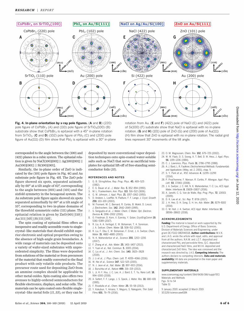
corresponded to the angle between the (100) and(422) planes in a cubic system. The epitaxial rela-tion is given by NaCl(100)[001] || Ag(100)[001] ||Au(100)[001] || Si(100)[001].Similarly, the in-plane order of ZnO is indi-
cated by the (101) pole figure in Fig. 4G and Ausubstrate pole figure in Fig. 4H. The ZnO polefigure showed six spots, separated azimuth-ally by 60° at a tilt angle of 62°, correspondingto the angle between (001) and (101) and thesixfold symmetry in the hexagonal system. TheAu substrate pole figure again showed six spotsseparated azimuthally by 60° at a tilt angle of55°, corresponding to two in-plane domains ofthe threefold symmetric cubic (111) plane. Theepitaxial relation is given by ZnOð001Þ½110�∥Auð111Þ½10�1�∥Sið111Þ½10�1�.The spin coating of epitaxial films offers an
inexpensive and readily accessible route to single-crystal–like materials that should exhibit supe-rior electronic and optical properties owing tothe absence of high-angle grain boundaries. Awide range of materials can be deposited ontoa variety of wafer-sized substrates with unpre-cedented simplicity. The films were depositedfrom solutions of thematerial or from precursorsof the material that readily converted to the finalproduct with only volatile side products. Theprecursor route used for depositing ZnO froman ammine complex should be applicable toother metal oxides. Spin coating also offers twoavenues to highly-ordered semiconductors forflexible electronics, displays, and solar cells. Thematerials can be spin coated onto flexible single-crystal–like metal foils (11, 33), or they can be
deposited by more conventional vapor deposi-tion techniques onto spin-coated water-solublesalts such as NaCl that serve as sacrificial tem-plates for epitaxial lift-off of free-standing semi-conductor foils (31).
REFERENCES AND NOTES
1. G. B. Stringfellow, Rep. Prog. Phys. 45, 469–525(1982).
2. E. G. Bauer et al., J. Mater. Res. 5, 852–894 (1990).3. M. L. Frankenheim, Ann. Phys. 113, 516–522 (1836).4. G. W. Johnson, J. Appl. Phys. 21, 1057–1062 (1950).5. D. Andeen, L. Loeffler, N. Padture, F. F. Lange, J. Cryst. Growth
259, 103–109 (2003).6. M. Froment, M. C. Bernard, R. Cortès, B. Mokili, D. Lincot,
J. Electrochem. Soc. 142, 2642–2649 (1995).7. S. Sengupta et al., J. Mater. Chem. C Mater. Opt. Electron.
Devices 4, 1996–2002 (2016).8. O. Friedman, D. Korn, V. Ezersky, Y. Golan, CrystEngComm 19,
5381–5389 (2017).9. R. Liu, A. A. Vertegel, E. W. Bohannan, T. A. Sorenson,
J. A. Switzer, Chem. Mater. 13, 508–512 (2001).10. R. Liu, F. Oba, E. W. Bohannan, F. Ernst, J. A. Switzer, Chem.
Mater. 15, 4882–4885 (2003).11. N. K. Mahenderkar et al., Science 355, 1203–1206
(2017).12. F. Zhang et al., Adv. Mater. 25, 1401–1407 (2013).13. Y. Yuan et al., Nat. Commun. 5, 3005 (2014).14. C. Liu et al., J. Am. Chem. Soc. 140, 3825–3828
(2018).15. J. Li et al., J. Phys. Chem. Lett. 7, 4059–4066 (2016).16. W. Nie et al., Science 347, 522–525 (2015).17. N. J. Jeon et al., Nat. Mater. 13, 897–903 (2014).18. J. Burschka et al., Nature 499, 316–319 (2013).19. L. Ji, H.-Y. Hsu, J. C. Lee, A. J. Bard, E. T. Yu, Nano Lett. 18,
994–1000 (2018).20. A. Seifert, F. F. Lange, J. S. Speck, J. Mater. Res. 10, 680–691
(1995).21. F. Rivadulla et al., Chem. Mater. 25, 55–58 (2013).22. Y. Kokubun, Y. Amano, Y. Meguro, S. Nakagomi, Thin Solid
Films 601, 76–79 (2016).
23. O. M. Magnussen, Chem. Rev. 102, 679–725 (2002).24. W. W. Flack, D. S. Soong, A. T. Bell, D. W. Hess, J. Appl. Phys.
56, 1199–1206 (1984).25. C. J. Lawrence, Phys. Fluids 31, 2786–2795 (1988).26. A. J. Bard, L. R. Faulkner, Electrochemical Methods: Fundamentals
and Applications (Wiley, ed. 2, 2001), chap. 9.27. S. Y. Park et al., RSC Advances 4, 11295–11299
(2014).28. P. Prod’homme, F. Maroun, R. Cortès, P. Allongue, Appl. Phys.
Lett. 93, 171901 (2008).29. J. A. Switzer, J. C. Hill, N. K. Mahenderkar, Y.-C. Liu, ACS Appl.
Mater. Interfaces 8, 15828–15837 (2016).30. A. Janotti, C. G. Van de Walle, Rep. Prog. Phys. 72, 126501
(2009).31. D. K. Lee et al., Sci. Rep. 7, 8716 (2017).32. J. H. Heo, D. H. Song, S. H. Im, Adv. Mater. 26, 8179–8183
(2014).33. C. M. Hull, J. A. Switzer, ACS Appl. Mater. Interfaces 10,
38596–38602 (2018).
ACKNOWLEDGMENTS
Funding: The material is based on work supported by theU.S. Department of Energy, Office of Basic Sciences,Division of Materials Sciences and Engineering, undergrant DE-FG02-08ER46518. Author contributions: M.V.K.and J.A.S. wrote the article with input, edits, and approvalfrom all the authors. N.K.M. and J.Z.T. deposited andcharacterized PbI2 and perovskite films, Q.C. depositedand characterized NaCl films, and M.V.K. deposited andcharacterized ZnO films. The idea was conceived and theresearch was directed by J.A.S. Competing interests: Theauthors declare no competing interests. Data and materialsavailability: All data are presented in the main paper andsupplementary materials.
SUPPLEMENTARY MATERIALS
www.sciencemag.org/content/364/6436/166/suppl/DC1Materials and MethodsFigs. S1 to S4Table S1
9 January 2019; accepted 13 March 201910.1126/science.aaw6184
Kelso et al., Science 364, 166–169 (2019) 12 April 2019 4 of 4
Fig. 4. In-plane orientation by x-ray pole figures. (A and B) (220)pole figure of CsPbBr3 (A) and (110) pole figure of SrTiO3(100) (B)substrate show that CsPbBr3 is epitaxial with a 45° in-plane rotationfrom SrTiO3. (C and D) (102) pole figure of PbI2 (C) and (200) polefigure of Au(111) (D) film show that PbI2 is epitaxial with a 30° in-plane
rotation from Au. (E and F) (422) pole of NaCl (E) and (422) poleof Si(100) (F) substrate show that NaCl is epitaxial with no in-planerotation. (G and H) (101) pole of ZnO (G) and (200) pole of Au(111)(H) film show that ZnO is epitaxial with no in-plane rotation. The radial gridlines represent 30° increments of the tilt angle.
RESEARCH | REPORTon June 12, 2020
http://science.sciencemag.org/
Dow
nloaded from

Spin coating epitaxial filmsMeagan V. Kelso, Naveen K. Mahenderkar, Qingzhi Chen, John Z. Tubbesing and Jay A. Switzer
DOI: 10.1126/science.aaw6184 (6436), 166-169.364Science
, this issue p. 166Sciencefor perovskites, zinc oxide, and sodium chloride.−−oriented by the substrate
in which the crystallites are−−basis of its viscosity and the rotation rate. In this way, they achieved epitaxial growth performed spin coating with single-crystal substrates, carefully controlling the thickness of the spreading solution on the
et al.make polycrystalline inorganic coatings and amorphous films, such as polymers used in lithography. Kelso droplet of solution containing the coating is added at the center, spreads out, and evaporates. This method is used to
A simple way to coat a surface with a uniform film is by spin coating. The substrate is spun at high speed, and aEpitaxial films through spin coating
ARTICLE TOOLS http://science.sciencemag.org/content/364/6436/166
MATERIALSSUPPLEMENTARY http://science.sciencemag.org/content/suppl/2019/04/10/364.6436.166.DC1
CONTENTRELATED http://science.sciencemag.org/content/sci/365/6458/eaay3894.full
REFERENCES
http://science.sciencemag.org/content/364/6436/166#BIBLThis article cites 32 articles, 3 of which you can access for free
PERMISSIONS http://www.sciencemag.org/help/reprints-and-permissions
Terms of ServiceUse of this article is subject to the
is a registered trademark of AAAS.ScienceScience, 1200 New York Avenue NW, Washington, DC 20005. The title (print ISSN 0036-8075; online ISSN 1095-9203) is published by the American Association for the Advancement ofScience
Science. No claim to original U.S. Government WorksCopyright © 2019 The Authors, some rights reserved; exclusive licensee American Association for the Advancement of
on June 12, 2020
http://science.sciencemag.org/
Dow
nloaded from