thermal infrared emission from biased graphene infrared emission from biased graphene marcus...
TRANSCRIPT

Thermal infrared emission from biased grapheneMarcus Freitag*, Hsin-Ying Chiu, Mathias Steiner, Vasili Perebeinos and Phaedon Avouris
The high carrier mobility1,2 and thermal conductivity3,4 of gra-phene make it a candidate material for future high-speed elec-tronic devices5. Although the thermal behaviour of high-speeddevices can limit their performance, the thermal properties ofgraphene devices remain incompletely understood. Here, weshow that spatially resolved thermal radiation from biased gra-phene transistors can be used to extract the temperature distri-bution, carrier densities and spatial location of the Dirac pointin the graphene channel. The graphene exhibits a temperaturemaximum with a location that can be controlled by the gatevoltage. Stationary hot spots are also observed. Infrared emis-sion represents a convenient and non-invasive characterizationtool for graphene devices.
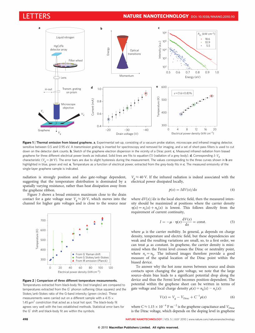
To explore the graphene thermal radiation, we fabricated large,back-gated transistors from exfoliated graphene. While passing acurrent through the graphene, electronic energy is transformedinto Joule heat, which is mainly dissipated into the substrate andthe metallic contacts6. A small fraction (,1026, see Methods) isradiated into free space, which can be detected spatially or spectrallyresolved in the near-infrared. Details of the experimental set-up(Fig. 1a) and sample fabrication can be found in the Methods.Figure 1c shows three (of a total of 11) infrared spectra, fitted to theformula for a grey body (Planck’s law, modified by an emissivity 1),
u n,T( ) = 18p
h2c3
hn( )3
exp hn/kBT − 1( ) (1)
where u is the spectral energy density, hn the photon energy and T thetemperature. Corresponding drain voltages and currents are shown inFig. 1d, while Fig. 1e shows the extracted temperatures. The good fitquality in Fig. 1c suggests that graphene indeed behaves like a greybody with constant emissivity, and deviations are of the order of+20%, a value that is likely limited by uncertainties in the opticalsystem response rather than the graphene emissivity itself.
After calibration with a black-body source of known temperatureand emissivity, an emissivity value of 1¼ (1.6+0.8)% was extracted.This value is in reasonable agreement with the measured absorptiv-ity a¼ 2.3% for single-layer graphene7,8. It is important to note thatour graphene samples are electrically biased and therefore coulddeviate from thermal equilibrium. Nevertheless, we found thatKirchhoff’s law holds within experimental errors in the measuredphoton energy range 0.5–0.95 eV.
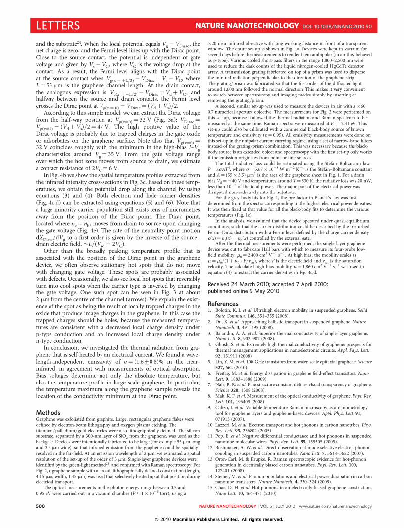
The validity of the temperature measurement by means ofthermal emission was confirmed using another sample, for whichwe applied two established methods to extract the local temperature(see Fig. 2). In the first, Raman Stokes/anti-Stokes measurementswere used to determine the temperature by measuring the phononoccupation number n of the G-phonon band:
IS
IAS= 1 + n
nEL − h−vEL + h−v
( )3xS
xAS
( )2
≈ exph−vkT
( )EL − h−vEL + h−v
( )3
(2)
where h−v is the energy of the G phonon, EL is the laser excitationenergy, and xS,AS are Stokes/anti-Stokes Raman susceptibilities.Because the graphene absorption is essentially constant, xS andxAS are the same, and the measurements can be performed at thesame value of EL. In the second method, use is made of the factthat the shift of the Raman G′ band scales with temperature asDvG′/DT¼20.034 cm21 K21 (ref. 9). Both Raman methodsshow good agreement with the temperatures extracted from thethermal radiation.
Recently, non-equilibrium phonon distributions have beenfound in electrically heated carbon nanotubes10–14. In this case,the optical phonons G and G′, as well as intermediate-frequencyphonons, are populated at much higher ‘temperatures’ than theradial-breathing mode (RBM) and other acoustic phonons. In ourmeasurements, the infrared emission in graphene represents anelectronic temperature, the Stokes/anti-Stokes temperature rep-resents the temperature of the G-phonons, and the G′ Ramanshift represents the temperature of the phonons to which G′ anhar-monically couples. The close agreement of all three temperaturessuggests that no significant non-equilibrium phonon distributionexists in graphene at least up to 700 K.
A non-equilibrium G-band phonon population was recentlyobserved in another experiment15. There, the temperature derivedfrom G-band Stokes/anti-Stokes measurements was much larger(1,500 K) than the temperature derived from the G-band redshift(500 K). It is possible that the strong local electric fields in a smallconstriction were sufficient to drive the G-band phonon populationout of equilibrium. The authors have also shown that the constric-tion emits visible light that can be detected by a charge-coupleddevice (CCD) camera when biased close to breakdown.
We next considered the spatial variation of infrared emissionand, therefore, the temperature distribution along the biased gra-phene sample (Fig. 3). Graphene has a high room-temperaturethermal conductivity, kGr¼ 5,000 W m21 K21 (refs 3,4), so partof the heat is carried laterally into the metallic contacts6,16.However, Umklapp scattering reduces this value at elevated temp-eratures17–19, and surface polar phonon scattering enhances theenergy transfer to the SiO2 substrate6,20–23. For devices that arelonger than a few micrometres as in our case, heat transfer intothe substrate dominates6:
T(x) = Tsub + p(x)/g (3)
where Tsub¼ 293 K is the substrate temperature, p(x) is the locallygenerated power, and g is the effective thermal conductivity of thesubstrate, which depends on the thermal coupling between gra-phene and the SiO2. If p(x) were position-independent, we wouldexpect a flat temperature distribution in the centre of the device.Temperature drops should be limited to the immediate vicinity ofthe contact areas, where lateral thermal transport along the gra-phene sheet can compete with thermal transport into the sub-strate6,16. In contrast, we observe in Fig. 3a that the infrared
IBM Thomas J. Watson Research Center, Yorktown Heights, New York 10598, USA. *e-mail: [email protected]
LETTERSPUBLISHED ONLINE: 9 MAY 2010 | DOI: 10.1038/NNANO.2010.90
NATURE NANOTECHNOLOGY | VOL 5 | JULY 2010 | www.nature.com/naturenanotechnology 497
© 2010 Macmillan Publishers Limited. All rights reserved.
radiation is strongly position and also gate-voltage dependent,suggesting that the temperature distribution is dominated by aspatially varying resistance, rather than heat dissipation away fromthe graphene ribbon.
Figure 3 shows a broad emission maximum close to the draincontact for a gate voltage near Vg ≈ 20 V, which moves into thechannel for higher gate voltages and is close to the source near
Vg ≈ 40 V. If the infrared radiation is indeed associated with theelectrical power dissipated locally,
p(x) = IdV(x)/dx (4)
where dV(x)/dx is the local electric field, then the measured inten-sity should be maximized at positions where the carrier densityh(x)¼ ne(x)þ nh(x) is lowest. This follows directly from therequirement of current continuity,
I = −m · h x( ) dV(x)dx
= const. (5)
where m is the carrier mobility. In general, m depends on chargedensity, temperature and electric field, but these dependencies areweak and the resulting variations are small, so, to a first order, wecan treat m as constant. In graphene, the carrier density is mini-mized when the Fermi level crosses the Dirac or neutrality point,where ne¼ nh. The infrared images therefore provide a goodmeasure of the spatial location of the Dirac point within thebiased device.
To answer why the hot zone moves between source and draincontacts upon changing the gate voltage, we note that the largesource–drain bias leads to a significant potential drop along thedevice and thus the Fermi level becomes position-dependent. Thepotential within the graphene sheet can be written in terms ofgate voltage and local charge density r(x)¼ nh(x) 2 ne(x):
V(x) = Vg − VDirac + C−1r(x) (6)
where C ≈ 1.15 × 1024 F m22 is the graphene capacitance and VDiracis the Dirac voltage, which depends on the doping level in graphene
0.5 0.6 0.7 0.8 0.9 1.0
102
103
104
105
106 PEL (kW cm–2)
18.6 10.9 5.5
Inte
nsity
(a.u
.)
Energy (eV)
−20 −30 −400.4
0.6
0.8
1.0C
urre
nt (m
A)
Drain voltage (V)
d
a c
e
b
Liquid nitrogen
HgCdTedetector array
Filter wheel
Lens
Graphene
Microscopeobjective
Transm. gratingon prism
in-out
Vg
Vd
Vs
Opticaltransitions
Momentum
Ener
gy
300
400
500
600
Tem
pera
ture
(K)
Electrical power density (kW cm−2)
ε = (1.6 ± 0.8)%
0 4 8 12 16 20
Figure 1 | Thermal emission from biased graphene. a, Experimental set-up, consisting of a vacuum probe station, microscope and infrared imaging detector,
sensitive between 0.5 and 0.95 eV. A transmission grating is inserted for spectroscopy and removed for imaging, and a set of short-pass filters is used to cut
down on the detector dark counts. b, Sketch of the graphene electron dispersion in the vicinity of a Dirac point. c, Measured infrared radiation from biased
graphene for three different electrical power levels as indicated. Solid lines are fits to equation (1) (radiation of a grey body). d, Corresponding I–Vd
characteristic (Vg¼ 20 V). The error bars are due to slight hysteresis during the measurement. The values corresponding to the three curves shown in b are
highlighted in blue, green and red. e, Temperature as a function of electrical power, extracted from the grey-body fits in c. The measured emissivity of the
single-layer graphene sample is indicated.
0 20 40 60 80 100 120
300
400
500
600
700
Tem
pera
ture
(K)
Electrical power density (kW cm–2)
From G' Raman shiftFrom G Stokes/anti-StokesFrom IR emission (Planck)
Figure 2 | Comparison of three different temperature measurements.
Temperatures extracted from black-body fits (red triangles) are compared to
temperatures extracted from the G′ phonon softening (blue squares) and the
Stokes/anti-Stokes ratio of the G-band intensity (green circles). These
measurements were carried out on a different sample with a 4.15×1.45 mm2 constriction that acted as a local hot spot. The black-body fit
agrees very well with the two established methods. Statistical error bars for
the G′ shift and black-body fit are within the symbols.
LETTERS NATURE NANOTECHNOLOGY DOI: 10.1038/NNANO.2010.90
NATURE NANOTECHNOLOGY | VOL 5 | JULY 2010 | www.nature.com/naturenanotechnology498
© 2010 Macmillan Publishers Limited. All rights reserved.

0.52
0.54
0.56
0.58
0.60
0.62
0.64
0.66 Vd = −30 V
Cur
rent
(mA
)
Gate voltage (V)
Sweep direction
bGate voltage
21.1 V22.3 V23.4 V24.6 V25.7 V26.9 V28.0 V29.1 V
30.3 V31.4 V32.6 V33.7 V34.9 V36.0 V37.1 V38.3 V39.4 V
Dirac (neutrality) point
21.1 V 25.7 V 30.3 V 34.9 V 39.4 V
S
D
Mainly electrons
Mainly holes55
µm
SEM
20 25 30 35 40 –40 –30 –20 –10 0 10 20 30 400.00.20.40.60.81.01.21.41.61.82.0
Cou
nts
(a.u
.)
Position (µm)
−30 V 0 Vc
Intensity(a.u.) 0 1
a
Figure 3 | Bias-dependent thermal images of graphene. a, Spatial images of the integrated infrared emission (with wavelength up to 2,000 nm) from the
graphene sample from Fig. 1. The drain bias was Vd¼230 V and the gate voltages varied between Vg¼ 20 V and 40 V, as indicated. The scanning electron
microscopy (SEM) image shows the graphene contacted by source (S) and drain (D) contacts. The graphene becomes hottest at the position of the Dirac
point, which can be moved by the gate voltage. The white line is a guide to the eye. A video of the sequence is available online. b, Corresponding I–Vg
characteristic. c, Infrared intensity profile along the length of the graphene sample, extracted from the images in a. The dashed lines mark the position of
drain and source contacts. The arrows point to a local hot spot under hole conduction that reversibly turns into a cold spot under electron conduction.
0.0
0.4
0.8
1.2
1.6
nh
ne
Vg = 39.4 V
n e,h
(1012
cm
−2)
d
−20 −10 0 10 20Position (µm)
0.0
0.4
0.8
1.2
1.6nh
ne
Vg = 21.1 V
n e,h
(1012
cm
−2)
c
−20 −10 0 10 20Position (µm)
−20 −10 0 10 20
20
25
30
35
40
V g (V
)
Position (µm)
e
Dirac (neutrality)point position
Hole
ElectronEFEDirac
a
Dirac (neutrality) point
−20 −10 0 10 20Position (µm)
420
440
460
480
Gate voltage 21.1 V39.4 VTe
mpe
ratu
re (K
)
b
−20 −10 0 10 20Position (µm)
Figure 4 | Temperatures, charge carriers and the position of the Dirac point during gate-voltage sweeps. a, Schematic of the Fermi level within the
graphene device in the ambipolar regime. b, Temperature profile along the graphene sample for the different gate voltages, extracted from the infrared
intensity images in Fig. 3c. c,d, Electron and hole distribution in the device for Vg¼ 21.1 V (c) and Vg¼ 39.4 V (d) using measured temperatures and
equation (3–6) with high-field mobility m¼ 1,860 cm2 V21 s21 and contact resistance 2VC¼ 6 V. e, Dirac (neutrality) point position versus gate voltage.
The solid line is a linear fit.
NATURE NANOTECHNOLOGY DOI: 10.1038/NNANO.2010.90 LETTERS
NATURE NANOTECHNOLOGY | VOL 5 | JULY 2010 | www.nature.com/naturenanotechnology 499
© 2010 Macmillan Publishers Limited. All rights reserved.
and the substrate24. When the local potential equals Vg 2 VDirac, thenet charge is zero, and the Fermi level lines up with the Dirac point.Close to the source contact, the potential is independent of gatevoltage and given by Vs 2 VC, where VC is the voltage drop at thecontact. As a result, the Fermi level aligns with the Dirac pointat the source contact when Vg(x ¼ þL/2) 2 VDirac¼Vs 2 VC, whereL¼ 55 mm is the graphene channel length. At the drain contact,the analogous expression is Vg(x ¼ 2L/2) 2 VDirac¼VdþVC, andhalfway between the source and drain contacts, the Fermi levelcrosses the Dirac point at Vg(x ¼ 0) 2 VDirac¼ (Vdþ Vs)/2.
According to this simple model, we can extract the Dirac voltagefrom the half-way position at Vg(x¼0)¼ 32 V (Fig. 3a): VDirac¼Vg(x¼0) 2 (Vdþ Vs)/2¼ 47 V. The high positive value of theDirac voltage is probably due to trapped charges in the gate oxideor adsorbates on the graphene surface. Note also that Vg(x¼0)¼32 V coincides roughly with the minimum in the high-bias I–Vgcharacteristics around Vg¼ 35 V. From the gate voltage rangeover which the hot zone moves from source to drain, we estimatea contact resistance of 2VC¼ 6 V.
In Fig. 4b we show the spatial temperature profiles extracted fromthe infrared intensity cross-sections in Fig. 3c. Based on these temp-eratures, we obtain the potential drop along the channel by usingequations (3) and (4). Both electron and hole carrier densities(Fig. 4c,d) can be extracted using equations (5) and (6). Note thata large minority carrier population still exists tens of micrometresaway from the position of the Dirac point. The Dirac point,located where ne¼ nh, moves from drain to source upon changingthe gate voltage (Fig. 4e). The rate of the neutrality point motiondXDirac/dVg to a first order is given by the inverse of the source–drain electric field, �L/(Vsd 2 2VC).
Other than the broadly peaking temperature profile that isassociated with the position of the Dirac point in the graphenedevice, we often observe stationary hot spots that do not movewith changing gate voltage. These spots are probably associatedwith defects. Occasionally, we also see local hot spots that reversiblyturn into cool spots when the carrier type is inverted by changingthe gate voltage. One such spot can be seen in Fig. 3 at about2 mm from the centre of the channel (arrows). We explain the exist-ence of the spot as being the result of locally trapped charges in theoxide that produce image charges in the graphene. In this case thetrapped charges should be holes, because the measured tempera-tures are consistent with a decreased local charge density underp-type conduction and an increased local charge density undern-type conduction.
In conclusion, we investigated the thermal radiation from gra-phene that is self-heated by an electrical current. We found a wave-length-independent emissivity of 1¼ (1.6+0.8)% in the near-infrared, in agreement with measurements of optical absorption.Bias voltages determine not only the absolute temperature, butalso the temperature profile in large-scale graphene. In particular,the temperature maximum along the graphene sample reveals thelocation of the conductivity minimum at the Dirac point.
MethodsGraphene was exfoliated from graphite. Large, rectangular graphene flakes weredefined by electron-beam lithography and oxygen plasma etching. Thetitanium/palladium/gold electrodes were also lithographically defined. The siliconsubstrate, separated by a 300-nm layer of SiO2 from the graphene, was used as thebackgate. Devices were intentionally fabricated to be large (for example 55 mm longand 3.5 mm wide), so that infrared emission from the graphene could be spatiallyresolved in the far-field. At an emission wavelength of 2 mm, we estimated a spatialresolution of the set-up of the order of 3 mm. Single-layer graphene devices wereidentified by the green-light method25, and confirmed with Raman spectroscopy. ForFig. 2, a graphene sample with a broad, lithographically defined constriction (length,4.15 mm; width, 1.45 mm) was used that selectively heated up at that position duringelectrical transport.
The optical measurements in the photon energy range between 0.5 and0.95 eV were carried out in a vacuum chamber (P ≈ 1 × 1025 torr), using a
×20 near-infrared objective with long working distance in front of a transparentwindow. The entire set-up is shown in Fig. 1a. Devices were kept in vacuum forseveral days before the measurements to render them ambipolar (in air they behavedas p-type). Various cooled short-pass filters in the range 1,800–2,500 nm wereused to reduce the dark counts of the liquid nitrogen-cooled HgCdTe detectorarray. A transmission grating fabricated on top of a prism was used to dispersethe infrared radiation perpendicular to the direction of the graphene strip.The grating/prism was fabricated so that the first order of the diffracted lightaround 1,600 nm followed the normal direction. This makes it very convenientto switch between spectroscopy and imaging modes simply by inserting orremoving the grating/prism.
A second, similar set-up was used to measure the devices in air with a ×600.7 numerical aperture objective. The measurements for Fig. 2 were performed onthis set-up, because it allowed the thermal radiation and Raman spectrum to bemeasured at the same time. Raman spectra were measured at EL¼ 2.41 eV. Thisset-up could also be calibrated with a commercial black-body source of knowntemperature and emissivity (1¼ 0.95). All emissivity measurements were done onthis set-up in the unipolar current carrying regime, using a set of narrow-band filtersinstead of the grating/prism combination. This was necessary because the black-body source is an extended object and spectroscopy with the first set-up only worksif the emission originates from point or line sources.
The total radiative loss could be estimated using the Stefan–Boltzmann lawP¼ 1sAT4, where s¼ 5.67 × 1028 W m22 K24 is the Stefan–Boltzmann constantand A¼ (55 × 3.5) mm2 is the area of the graphene sheet in Fig. 1. For a drainbias Vd¼240 V and temperatures around T¼ 530 K, the radiative loss was 20 nW,less than 1026 of the total power. The major part of the electrical power wasdissipated non-radiatively into the substrate.
For the grey-body fits for Fig. 1, the pre-factor in Planck’s law was firstdetermined from the spectra corresponding to the highest electrical power densities.It was then fixed at that value for all the black-body fits to determine the varioustemperatures (Fig. 1e).
In the analysis, we assumed that the device operated under quasi-equilibriumconditions, such that the carrier distribution could be described by the perturbedFermi–Dirac distribution with a Fermi level defined by the charge carrier densityr(x)¼ ne(x) 2 nh(x) controlled by the external gate.
After the thermal measurements were performed, the single-layer graphenedevice was cut to fabricate Hall bars with which to measure its four-probe low-field mobility: m0¼ 2,400 cm2 V21 s21. At high bias, the mobility scales asm¼m0/(1þ m0
. F/vsat), where F is the electric field and vsat is the saturationvelocity. The calculated high-bias mobility m¼ 1,860 cm2 V21 s21 was used inequation (4) to extract the carrier densities in Fig. 4c,d.
Received 24 March 2010; accepted 7 April 2010;published online 9 May 2010
References1. Bolotin, K. I. et al. Ultrahigh electron mobility in suspended graphene. Solid
State Commun. 146, 351–355 (2008).2. Du, X. et al. Approaching ballistic transport in suspended graphene. Nature
Nanotech. 3, 491–495 (2008).3. Balandin, A. A. et al. Superior thermal conductivity of single-layer graphene.
Nano Lett. 8, 902–907 (2008).4. Ghosh, S. et al. Extremely high thermal conductivity of graphene: prospects for
thermal management applications in nanoelectronic circuits. Appl. Phys. Lett.92, 151911 (2008).
5. Lin, Y. M. et al. 100-GHz transistors from wafer-scale epitaxial graphene. Science327, 662 (2010).
6. Freitag, M. et al. Energy dissipation in graphene field-effect transistors. NanoLett. 9, 1883–1888 (2009).
7. Nair, R. R. et al. Fine structure constant defines visual transparency of graphene.Science 320, 1308 (2008).
8. Mak, K. F. et al. Measurement of the optical conductivity of graphene. Phys. Rev.Lett. 101, 196405 (2008).
9. Calizo, I. et al. Variable temperature Raman microscopy as a nanometrologytool for graphene layers and graphene-based devices. Appl. Phys. Lett. 91,071913 (2007).
10. Lazzeri, M. et al. Electron transport and hot phonons in carbon nanotubes. Phys.Rev. Lett. 95, 236802 (2005).
11. Pop, E. et al. Negative differential conductance and hot phonons in suspendednanotube molecular wires. Phys. Rev. Lett. 95, 155505 (2005).
12. Bushmaker, A. W. et al. Direct observation of mode selective electron phononcoupling in suspended carbon nanotubes. Nano Lett. 7, 3618–3622 (2007).
13. Oron-Carl, M. & Krupke, R. Raman spectroscopic evidence for hot-phonongeneration in electrically biased carbon nanotubes. Phys. Rev. Lett. 100,127401 (2008).
14. Steiner, M. et al. Phonon populations and electrical power dissipation in carbonnanotube transistors. Nature Nanotech. 4, 320–324 (2009).
15. Chae, D.-H. et al. Hot phonons in an electrically biased graphene constriction.Nano Lett. 10, 466–471 (2010).
LETTERS NATURE NANOTECHNOLOGY DOI: 10.1038/NNANO.2010.90
NATURE NANOTECHNOLOGY | VOL 5 | JULY 2010 | www.nature.com/naturenanotechnology500
© 2010 Macmillan Publishers Limited. All rights reserved.

16. Connolly, M. R. et al. Scanning gate microscopy of current-annealed single layergraphene. Appl. Phys. Lett. 96, 113501 (2010).
17. Berber, S., Kwon, Y.-K. & Tomanek, D. Unusually high thermal conductivity ofcarbon nanotubes. Phys. Rev. Lett. 84, 4613–4616 (2000).
18. Osman, M. A. & Srivastava, D. Temperature dependence of the thermalconductivity of single-wall carbon nanotubes. Nanotechnology 12, 21–24 (2001).
19. Nika, D. L. et al. Phonon thermal conduction in graphene: role of Umklapp andedge roughness scattering. Phys. Rev. B 79, 155413 (2009).
20. Chen, J.-H. et al. Intrinsic and extrinsic performance limits of graphene deviceson SiO2. Nature Nanotech. 3, 206–209 (2008).
21. Meric, I. et al. Current saturation in zero-bandgap, top-gated graphenefield-effect transistors. Nature Nanotech. 3, 654–659 (2008).
22. Fratini, S. & Guinea, F. Substrate-limited electron dynamics in graphene. Phys.Rev. B 77, 195415 (2008).
23. Rotkin, S. V. et al. An essential mechanism of heat dissipation in carbonnanotube electronics. Nano Lett. 9, 1850–1855 (2009).
24. Tersoff, J. et al. Device modeling of long-channel nanotube electro-opticalemitter. Appl. Phys. Lett. 86, 263108 (2005).
25. Blake, P. et al. Making graphene visible. Appl. Phys. Lett. 91, 063124 (2007).
Author contributionsAll authors contributed to the preparation of this manuscript.
Additional informationThe authors declare no competing financial interests. Supplementary informationaccompanies this paper at www.nature.com/naturenanotechnology. Reprints andpermission information is available online at http://npg.nature.com/reprintsandpermissions/.Correspondence and requests for materials should be addressed to M.F.
NATURE NANOTECHNOLOGY DOI: 10.1038/NNANO.2010.90 LETTERS
NATURE NANOTECHNOLOGY | VOL 5 | JULY 2010 | www.nature.com/naturenanotechnology 501
© 2010 Macmillan Publishers Limited. All rights reserved.