thermal aware floor planning tool by - … aware floor planning tool by gautam morab a report...
TRANSCRIPT
THERMAL AWARE FLOOR PLANNING TOOL
by
Gautam Morab
A report submitted in partial fulfillmentof the requirements for the degree
of
MASTER OF SCIENCE
in
Computer Engineering
Approved:
Dr. Sanghamitra Roy Dr. Koushik ChakrabortyMajor Professor Committee Member
Dr. Edmund SpencerCommittee Member
UTAH STATE UNIVERSITYLogan, Utah
2010

ii
Copyright c© Gautam Morab 2010
All Rights Reserved
iii
Abstract
Thermal Aware Floor Planning Tool
by
Gautam Morab, Master of Science
Utah State University, 2010
Major Professor: Dr. Sanghamitra RoyDepartment: Electrical and Computer Engineering
With every new process generation, the power density of microprocessors is increasing.
As a result, maximum chip temperature has increased considerably. The high temperature
of the chip has many adverse effects. It greatly affects the reliability of the chip, raises the
leakage power consumed by the chip to an unprecedented level, and makes cooling solutions
for the chip significantly more expensive. Apart from the power density of the blocks, the
high temperature also depends on power density of the neighboring blocks. Consequently,
the placement of blocks in the architecture of the chip, or a particular floor plan selected
for a given chip, can affect the maximum temperature of the chip to a very large extent.
This project is development of a thermal aware floor planning tool. It makes use of
HotSpot 5.0 temperature modeling tool and Parquet floor planning tool. Both HotSpot
and Parquet are open-source software and can be downloaded by anyone. HotSpot is used
to calculate the maximum temperature of the floor plan and the maximum temperature
thus calculated is included to the objective function of Parquet for performing simulated
annealing based floor planning.
HotSpot tool has been developed by the University of Virginia. HotSpot is an accurate
and fast thermal modeling tool suitable for use in architectural studies. For every floor
plan, HotSpot generates an equivalent circuit of thermal resistances and capacitances. The
iv
equivalent circuit of thermal resistances and capacitances corresponds to microarchitectural
blocks and essential aspects of the thermal package. HotSpot has a simple set of interfaces.
Hence, most power-performance simulators like Wattch can be integrated with Hotspot.
The main advantage of HotSpot is its compatibility with the kinds of power/performance
models used in the computer architecture community.
Parquet is the software for floor planning based on simulated annealing algorithm. It
has been used in a number of projects in computer-aided design and computer architecture.
While originally designed for fixed-outline floor planning, it can also be applied to classical
min-area block packing. The internal floor plan representation alternates between sequence
pairs and B*-trees data structures.
The thermal aware floor planning tool developed in this project was run on several
MCNC and GSRC benchmarks and it was found that the tool achieves temperature reduc-
tion of around 5-20%. In one of the benchmarks, temperature reduction observed was as
high as 30◦C. Also, the penalties on the total chip area and wire length were found to be
minimal.
(49 pages)

v
Acknowledgments
I owe my deepest gratitude to my advisor, Dr. Sanghamitra Roy, whose encouragement
and guidance from the start enabled me to finish this project. I would not have been able
to complete this project without her help. I would also like to thank the members of
my graduate committee, Dr. Koushik Chakraborty and Dr. Edmund Spencer, for their
guidance and suggestions.
I thank the Department of Electrical and Computer Engineering for providing the
support and the infrastructure I needed to produce and complete my project.
My sincere thanks to my friends: Arti, Akshata, Miti, Sagar, and Swadesh for their
constant encouragement and emotional support.
Finally, I would like to thank my family: my father, Mr. Jagdish Morab; my mother,
Mrs. Sushma Morab; my sister, Mrs. Meghna Kulkarni; and my late grandmother, Mrs.
Pramila Morab, for instilling in me confidence and a drive for pursuing my master’s degree.
They have always been my source of inspiration and strength throughout my life.
Gautam Morab
vi
Contents
Page
Abstract . . . . . . . . . . . . . . . . . . . . . . . . . . . . . . . . . . . . . . . . . . . . . . . . . . . . . . . iii
Acknowledgments . . . . . . . . . . . . . . . . . . . . . . . . . . . . . . . . . . . . . . . . . . . . . . . v
List of Figures . . . . . . . . . . . . . . . . . . . . . . . . . . . . . . . . . . . . . . . . . . . . . . . . . . vii
1 Introduction . . . . . . . . . . . . . . . . . . . . . . . . . . . . . . . . . . . . . . . . . . . . . . . . . 1
1.1 Need for Thermal Aware Design . . . . . . . . . . . . . . . . . . . . . . . . 11.2 Floor Planning . . . . . . . . . . . . . . . . . . . . . . . . . . . . . . . . . . 31.3 Project Objective . . . . . . . . . . . . . . . . . . . . . . . . . . . . . . . . . 5
2 Literature Review and Related Background . . . . . . . . . . . . . . . . . . . . . . . 7
2.1 Literature Review . . . . . . . . . . . . . . . . . . . . . . . . . . . . . . . . 72.2 Related Background . . . . . . . . . . . . . . . . . . . . . . . . . . . . . . . 9
2.2.1 Parquet Floor Planner . . . . . . . . . . . . . . . . . . . . . . . . . . 102.2.2 HotSpot . . . . . . . . . . . . . . . . . . . . . . . . . . . . . . . . . . 10
3 Thermal Aware Floor Planning Tool . . . . . . . . . . . . . . . . . . . . . . . . . . . . . 12
3.1 Problem Definition . . . . . . . . . . . . . . . . . . . . . . . . . . . . . . . . 133.2 Salient Features of the Tool . . . . . . . . . . . . . . . . . . . . . . . . . . . 13
3.2.1 Parquet Floor Planner . . . . . . . . . . . . . . . . . . . . . . . . . . 143.2.2 Simulated Annealing . . . . . . . . . . . . . . . . . . . . . . . . . . . 173.2.3 Objective Function for Simulated Annealing . . . . . . . . . . . . . . 193.2.4 HotSpot Thermal Modeling Tool . . . . . . . . . . . . . . . . . . . . 21
3.3 Interfacing of HotSpot and Parquet . . . . . . . . . . . . . . . . . . . . . . . 23
4 Results . . . . . . . . . . . . . . . . . . . . . . . . . . . . . . . . . . . . . . . . . . . . . . . . . . . . . . 25
4.1 Generation of Ptrace File . . . . . . . . . . . . . . . . . . . . . . . . . . . . 254.2 Testing . . . . . . . . . . . . . . . . . . . . . . . . . . . . . . . . . . . . . . 264.3 Results Obtained From the Tool . . . . . . . . . . . . . . . . . . . . . . . . 27
4.3.1 Effect of Thermal Aware Floor Planning on Temperature . . . . . . 274.3.2 Effect of Thermal Aware Floor Planning on Area of the Chip . . . . 284.3.3 Effect of Thermal Aware Floor Planning on Wire Length . . . . . . 294.3.4 Effect of Thermal Aware Floor Planning on the Placement of the Blocks 294.3.5 Effect of Thermal Aware Floor Planning on Execution Time . . . . 32
4.4 New Implementation of the Interface Between Parquet and HotSpot . . . . 33
5 Conclusion and Future Work . . . . . . . . . . . . . . . . . . . . . . . . . . . . . . . . . . . . 36
References . . . . . . . . . . . . . . . . . . . . . . . . . . . . . . . . . . . . . . . . . . . . . . . . . . . . . . 37
Appendix . . . . . . . . . . . . . . . . . . . . . . . . . . . . . . . . . . . . . . . . . . . . . . . . . . . . . . 40
vii
List of Figures
Figure Page
1.1 Power density trend. . . . . . . . . . . . . . . . . . . . . . . . . . . . . . . . 6
1.2 Different floor plans of the same circuit. . . . . . . . . . . . . . . . . . . . . 6
1.3 Floor plan: (a)Hot blocks placed next to each other. (b)Hot blocks placedaway from each other. . . . . . . . . . . . . . . . . . . . . . . . . . . . . . . 6
3.1 Horizontal representation of a B*-tree. . . . . . . . . . . . . . . . . . . . . . 16
3.2 (a) Shows the vertical B*-tree of the horizontal B*-tree in Fig. 3.1. (b)Shows the reverse horizontal B*-tree of the B*-tree in Fig. 3.1. All blocksare packed to the top instead of the bottom. (c) Shows the reverse verticalB*-tree of the vertical B*- tree in (a). . . . . . . . . . . . . . . . . . . . . . 17
3.3 Simulated annealing algorithm. . . . . . . . . . . . . . . . . . . . . . . . . . 20
3.4 Interfacing of HotSpot with Parquet. . . . . . . . . . . . . . . . . . . . . . . 24
4.1 Example of a ptrace file. . . . . . . . . . . . . . . . . . . . . . . . . . . . . . 26
4.2 Comparison of maximum temperature of the chip due to normal floor plan-ning vs. thermal aware floor planning. . . . . . . . . . . . . . . . . . . . . . 28
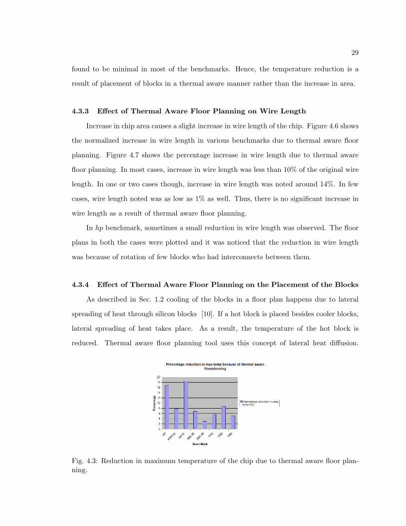
4.3 Reduction in maximum temperature of the chip due to thermal aware floorplanning. . . . . . . . . . . . . . . . . . . . . . . . . . . . . . . . . . . . . . 29
4.4 Comparison of area of the chip due to normal floor planning vs. thermalaware floor planning. . . . . . . . . . . . . . . . . . . . . . . . . . . . . . . . 30
4.5 Increase in area of the chip due to thermal aware floor planning. . . . . . . 30
4.6 Comparison of wire length of the chip due to normal floor planning vs. ther-mal aware floor planning. . . . . . . . . . . . . . . . . . . . . . . . . . . . . 30
4.7 Increase in wire length of the chip due to thermal aware floor planning. . . 31
4.8 Effect of thermal aware floor planning on the placement of the blocks. . . . 32
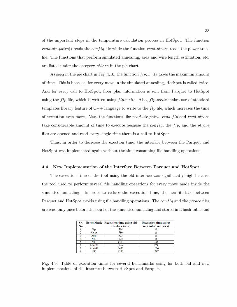
4.9 Table of execution times for several benchmarks using for both old and newimplementations of the interface between HotSpot and Parquet. . . . . . . . 33
4.10 Pie chart of time of execution of few of the important functions in the oldimplementation. . . . . . . . . . . . . . . . . . . . . . . . . . . . . . . . . . . 34
4.11 Pie chart of time of execution of few of the important functions in the newimplementation. . . . . . . . . . . . . . . . . . . . . . . . . . . . . . . . . . . 35
1
Chapter 1
Introduction
1.1 Need for Thermal Aware Design
In the last few years semiconductor industry has seen innumerable number of engi-
neering advances that has permitted a logarithmic growth in the capability of integrated
circuits (ICs). This trend was first publicized by Gordon E. Moore (co-founder of Intel) in
1965, who suggested that the number of transistors on an IC doubled every two year (his
observation is now known as Moore’s Law) [1].
Along with increasing number of transistors, the chip area has been decreasing at the
same rate [1]. As a result, elements are packed together at a very high density. Electric
current passing through a conventional conductor or semiconductor generates I2R Joules
of heat per second. Even though the current in each element of a modern microprocessor
is very small, owing to very high element density, a lot of heat needs to be dissipated from
a small surface area. Thus, modern microprocessors have very high power densities.
Power density of the microprocessors is also increasing with every new process genera-
tion since feature size and frequency are scaling faster than the operating voltage [2]. As a
result, there has been an increase in maximum chip temperatures because power density di-
rectly translates into heat. For example, Pentium 4 chips generate more heat than a kitchen
hotplate. If a Pentium 4 chip is allowed to run without a proper cooling system, it catches
fire [3]. Intel’s projections show that the heat generated by the processors will increase
sharply in the coming years, approaching that of the core of a nuclear power plant, unless
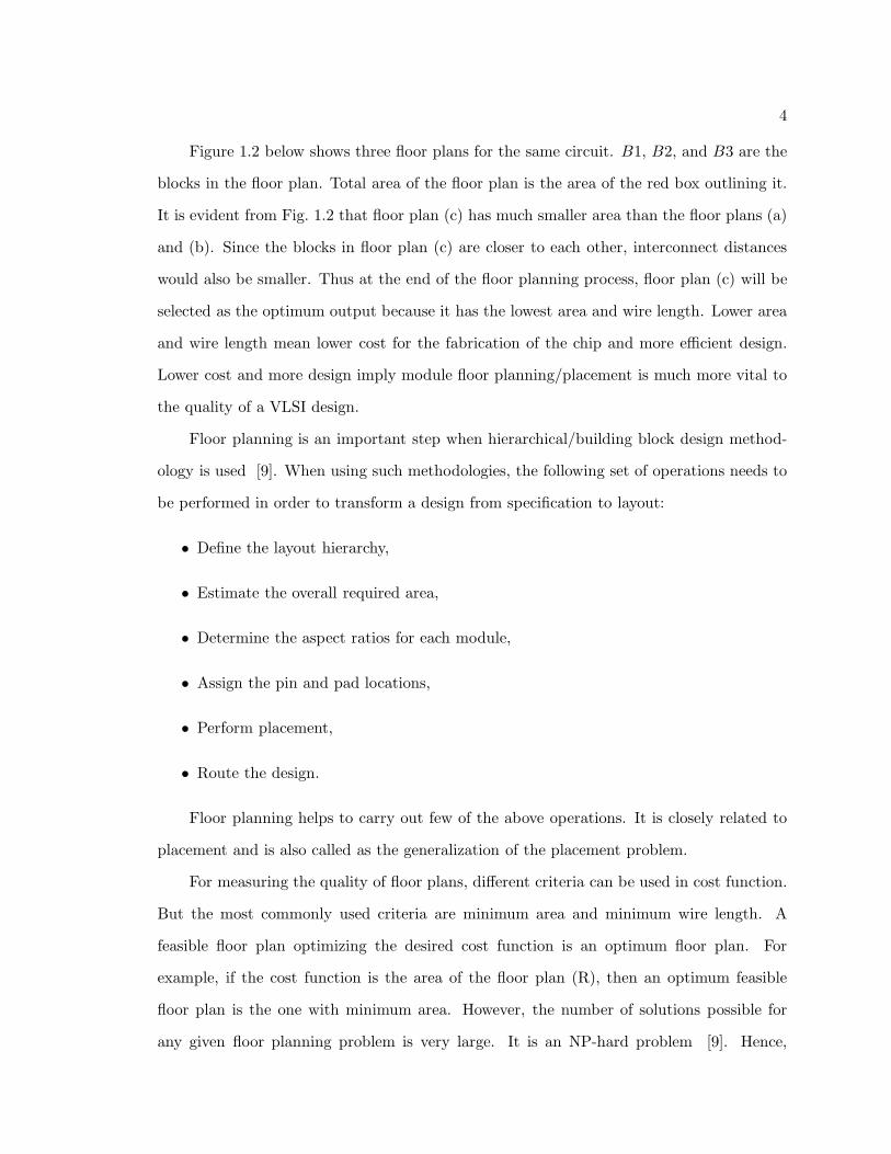
solutions to this problem can be found. Figure 1.1 ( [4]) gives an idea of the increasing
power densities in microprocessors.
In order to keep the chip temperatures below a limit, heat generated by the processor
2
must be removed from the die. We need properly designed cooling systems for that purpose.
But the cost of removing heat is also increasing at about the same rate as power density [5].
Reducing the maximum temperature in the chip can reduce the cost of the cooling system,
which constitutes a major component of the overall system cost.
Also, there are several negatives impacts of high processor temperatures. They are as
described below.
• The high temperature of the chip greatly affects its reliability. The reliability of the
chip reduces exponentially as the temperature increases. The time to failure has been
shown to be a function of
exp(−Ea/kT ), (1.1)
where Ea is the activation energy of the failure mechanism being accelerated by the
increased temperature, k is Boltzmann’s constant, and T is the absolute temperature
[6].
• With the reduction in feature size, leakage power consumption has become comparable
to the dynamic power consumption in a circuit. Leakage power is highly dependant
on temperature [7]. It increases exponentially with increase in temperature. Hence,
reducing the temperature of the chip will result in less leakage.
• Temperature has significant impact on microelectronic designs. Transistor speed is
slower at higher temperature because of the degradation of carrier mobility. Intercon-
nect metal resistivity is also dependent on temperature. For example, the resistivity
of copper increases by 39% from 20◦C to 120◦C. Higher resistivity causes longer in-
terconnect RC delay, and hence performance degradation.
Orthogonal to the power density of the functional blocks, another important factor
that affects the temperature distribution of a chip is the lateral spreading of heat in silicon
[8]. This depends on the functional unit adjacency determined by the floor plan of the
microprocessor. Traditionally, floor planning has been dealt with at a level closer to circuits
than to microarchitecture. One of the reasons for this is the level of detailed information
3
floor planning depends on, which is only available at the circuit level. However, with wire
delays dominating logic delays and temperature becoming a first class design constraint,
floor planning has started to be looked at even at the microarchitecture level. Floor planning
can be used to significantly decrease the maximum temperature in a chip.
1.2 Floor Planning
Owing to the growth in design complexity of circuits in recent times, the circuit sizes
are getting bigger. To take into consideration the increasing design complexity and larger
circuit sizes, hierarchical design and IP modules have been widely used. The circuits are
divided into number of structures or blocks by using a process known as circuit partitioning
[9]. Floor planning is the process of identifying structures that should be placed close
together, and allocating space for them so as to meet the sometimes conflicting goals of
required performance and available space (cost of the chip). Optimizing for minimum area
allows the design to use fewer resources. Also, it allows the sections of the design to be close
together. This leads to shorter interconnect distances, less routing resources to be used,
faster end-to-end signal paths, and even faster and more consistent place and route times.
Formal definition if floor planning problem is as given below.
• Input:
– n Blocks (B1, ..., Bn) with areas (A1, ..., An).
– Bounds ri and si on the aspect ratio of block Bi.
• Output:
– Coordinates (xi, yi), width wi and height hi for each block such that hi ∗wi = Ai
and ri = hi/wi = si.
• Objective:
– To optimize the circuit performance (optimize the cost function).
4
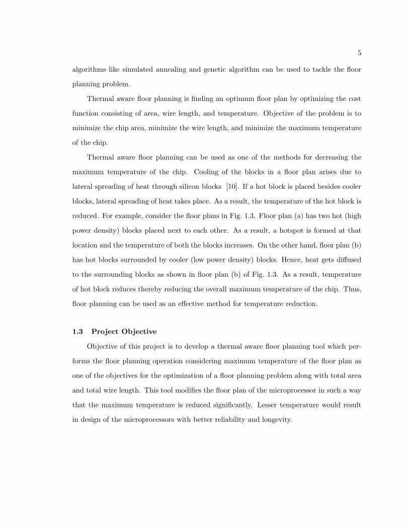
Figure 1.2 below shows three floor plans for the same circuit. B1, B2, and B3 are the
blocks in the floor plan. Total area of the floor plan is the area of the red box outlining it.
It is evident from Fig. 1.2 that floor plan (c) has much smaller area than the floor plans (a)
and (b). Since the blocks in floor plan (c) are closer to each other, interconnect distances
would also be smaller. Thus at the end of the floor planning process, floor plan (c) will be
selected as the optimum output because it has the lowest area and wire length. Lower area
and wire length mean lower cost for the fabrication of the chip and more efficient design.
Lower cost and more design imply module floor planning/placement is much more vital to
the quality of a VLSI design.
Floor planning is an important step when hierarchical/building block design method-
ology is used [9]. When using such methodologies, the following set of operations needs to
be performed in order to transform a design from specification to layout:
• Define the layout hierarchy,
• Estimate the overall required area,
• Determine the aspect ratios for each module,
• Assign the pin and pad locations,
• Perform placement,
• Route the design.
Floor planning helps to carry out few of the above operations. It is closely related to
placement and is also called as the generalization of the placement problem.
For measuring the quality of floor plans, different criteria can be used in cost function.
But the most commonly used criteria are minimum area and minimum wire length. A
feasible floor plan optimizing the desired cost function is an optimum floor plan. For
example, if the cost function is the area of the floor plan (R), then an optimum feasible
floor plan is the one with minimum area. However, the number of solutions possible for
any given floor planning problem is very large. It is an NP-hard problem [9]. Hence,
5
algorithms like simulated annealing and genetic algorithm can be used to tackle the floor
planning problem.
Thermal aware floor planning is finding an optimum floor plan by optimizing the cost
function consisting of area, wire length, and temperature. Objective of the problem is to
minimize the chip area, minimize the wire length, and minimize the maximum temperature
of the chip.
Thermal aware floor planning can be used as one of the methods for decreasing the
maximum temperature of the chip. Cooling of the blocks in a floor plan arises due to
lateral spreading of heat through silicon blocks [10]. If a hot block is placed besides cooler
blocks, lateral spreading of heat takes place. As a result, the temperature of the hot block is
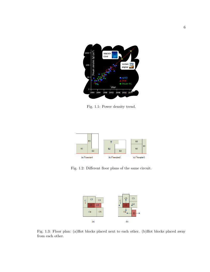
reduced. For example, consider the floor plans in Fig. 1.3. Floor plan (a) has two hot (high
power density) blocks placed next to each other. As a result, a hotspot is formed at that
location and the temperature of both the blocks increases. On the other hand, floor plan (b)
has hot blocks surrounded by cooler (low power density) blocks. Hence, heat gets diffused
to the surrounding blocks as shown in floor plan (b) of Fig. 1.3. As a result, temperature
of hot block reduces thereby reducing the overall maximum temperature of the chip. Thus,
floor planning can be used as an effective method for temperature reduction.
1.3 Project Objective
Objective of this project is to develop a thermal aware floor planning tool which per-
forms the floor planning operation considering maximum temperature of the floor plan as
one of the objectives for the optimization of a floor planning problem along with total area
and total wire length. This tool modifies the floor plan of the microprocessor in such a way
that the maximum temperature is reduced significantly. Lesser temperature would result
in design of the microprocessors with better reliability and longevity.
6
Fig. 1.1: Power density trend.
Fig. 1.2: Different floor plans of the same circuit.
Fig. 1.3: Floor plan: (a)Hot blocks placed next to each other. (b)Hot blocks placed awayfrom each other.
7
Chapter 2
Literature Review and Related Background
2.1 Literature Review
With the increase in the power density of circuits used in microprocessors, heat dis-
sipation has become one of the major factors in the microprocessor design. Thus many
methods have been developed for the reduction of the heat dissipation from the processors.
Floor planning is one of the methods of reducing heat from the processors.
Skadron et al. have proposed a thermal aware floor planning design using temperature
aware microarchitecture in their papers [8] [11]. They stress the significance of thermal
modeling; propose a compact, dynamic, and portable thermal model for easy use at the
architecture level; use this model to show that hot spots typically occur at the granular-
ity of architecture-level blocks, and discuss some remaining needs for further improving
the ability to evaluate temperature-aware methods. They call their model HotSpot [12].
HotSpot calculates the temperature distribution amongst different blocks on the CPU chip.
Using HotSpot, they evaluate a variety of dynamic thermal management techniques. They
have also developed a thermal aware floor planning tool called HotFloorPlanner [10]. Hot-
FloorPlanner is a floor planning tool, which makes use of function of area, wire length,
and temperature as objective and optimizes this objective using the simulated annealing
algorithm. It is very good software except that it can act only on slicing floor plans. It is
incapable of handling non-slicing floor plans.
Thermal design in sub-100nm technologies is even more difficult. It is one of the major
challenges to the CAD community. In the paper [13], authors Huang et al. introduce
the idea of temperature-aware design in every stage of ASIC/microprocessor design flow.
They propose a compact thermal model which can be integrated with modern CAD tools
8
to achieve a temperature-aware design methodology.
Chaparro et al. study the thermal-aware clustered microarchitectures [14]. They have
proposed several techniques including temperature aware steering techniques and cluster
hopping in a quad super scalar microarchitecture. Chu and Wong have talked about a new
combinatorial optimization problem [15]. They have proposed several good approximation
algorithms for the solution.
Donald and Martonosi [16] study temperature aware design issues for SMT (Simul-
taneous MultiThreading) and CMP (Chip Multiprocessing) architectures. According to
them, temperature gradients are important in both architectures but both show scope for
temperature aware enhancements to alleviate this problem. Li et al. [17] evaluate the ther-
mal efficiency for the SMT and CMP architectures. According to them, the SMT and CMP
architectures demonstrate similar peak operating temperatures. But the way by which they
heat up is quite different. As a result, the best thermal management mechanisms for them
are also different.
Hung et al. [18] make use of genetic algorithm to study thermal aware floor planning.
They make use of combined area and thermal optimization technique and show their tech-
nique decreases the peak temperature of floor plans. The generated floor plans using their
methods have areas comparable to the traditional area-oriented techniques.
Hung et al. [19] introduce Networks-on-chip (NoC), a new SoC paradigm. Authors
propose NoC as a solution to mitigate complex on-chip interconnects problems. NoC archi-
tecture consists of a collection of IP cores or processing elements (PEs) interconnected by
on-chip switching fabrics or routers. Hardware virtualization, which maps logic processing
units onto PEs, affects the power consumption of each PE and the communications among
PEs. The communication among PEs affects the overall performance and router power con-
sumption, and it depends on the placement of PEs. Therefore, the temperature distribution
profile of the chip depends on the IP core virtualization and placement. In this paper, they
present an IP virtualization and placement algorithm for generic regular network on chip
(NoC) architecture. The algorithm attempts to achieve a thermal balanced design while
9
minimizing the communication cost via placement.
2.2 Related Background
Han et al. [20] propose a floor planning tool based on Parquet [21]. The tool uses
the Parquet floor planner to carry out the basic simulated annealing process. Temperature
factor is added to the objective function of the tool by an approximation method know
as heat diffusion method. The idea is to surround the high-power density blocks with the
low-power density blocks so that the heat will diffuse from the high-power density block to
low-power density blocks surrounding it and would result in lower temperature of the block.
Overall, the maximum temperature of the whole chip is kept under a check.
In the paper [20], the authors prove that the temperature of an isolated block depends
linearly on its power density. They define the following measure as an approximation for
the heat diffusion between two adjacent blocks:
H(d1, d2) = (d1 − d2) ∗ shared length, (2.1)
where H is the heat diffusion, d1 and d2 are the power densities of the two blocks, and
shared length is the length of their shared boundary.
For each block, the total heat diffusion is:
H(d) = ΣH(d, di), for all its neighbors di. (2.2)
Rather than calculating the chip temperature, heat diffusion of the chip is calculated to
approximate temperature. Also, not all the blocks are considered. Only the heat diffusions
of blocks which may become the hottest (blocks with high-power density values) in the
chip are considered. Later the heat diffusion H of all the selected possibly-hot blocks is
calculated and added together. The total thermal diffusion D is defined as the sum of the
10
heat diffusion of all possibly-hot blocks:
D = ΣH(d), for all possibly-hot blocks. (2.3)
The final objective of Parquet floor planner is modified as follows:
Obj = CA ∗ A + CW ∗ W − CD ∗ D, (2.4)
where CA, CW , and CD are the weights of area, the wire length, and the heat diffusion,
respectively. CD has a negative sign because the thermal diffusion D needs to be maximized.
Thus in this method, the temperature part of the objective is a rough approximation.
A better approximation can be used which is more close to accurate. The thermal aware
floor planning tool developed in this project makes use of HotSpot tool [12] to approximate
the temperature part of the objective.
2.2.1 Parquet Floor Planner
Parquet is a floor planning tool developed at university of Michigan [22, 23]. The
Parquet floor planner is a fixed-outline/outline-free, hierarchical design package. It is an
open-source package and available to anyone. It is intended to solve multi-objective prob-
lems (area, wire length, etc.) using the simulated annealing algorithm. It is based on
the widely used sequence-pair representation. The more faster and efficient B*-trees rep-
resentation has also been added to the newer versions of Parquet. In fact, the floor plan
representation in Parquet alternates between the B*-trees and sequence pair representation
depending on number of blocks in the floor plan and the total desired whitespace. More
detailed description of Parquet is provided in Sec. 3.2.1.
2.2.2 HotSpot
HotSpot is an open source thermal modeling tool developed by university of Virginia.
It estimates the temperature of each block in the floor plan by constructing an equivalent

11
matrix made of thermal resistances and thermal capacitances. The tool developed in this
project uses HotSpot tool to calculate the maximum temperature amongst all the blocks
in the floor plan. The maximum temperature thus calculated is used in the objective
function of the simulated annealing routine inside the Parquet floor planner. More detailed
description of HotSpot is provided in Sec. 3.2.4.
12
Chapter 3
Thermal Aware Floor Planning Tool
This project is development of a floor planning tool which is similar to the tool devel-
oped by Han et al. [20]. But in this project, instead of approximating the chip temperature
using heat diffusion technique, maximum temperature amongst all the blocks in a processor
is calculated using the HotSpot 5.0 tool [12]. Parquet floor planner is used, which makes use
of simulated annealing (Sec. 3.2.2) to carry out the floor planning process. The function of
maximum temperature (calculated from HotSpot), chip area and total wire length is used
as an objective to carry out the simulated annealing. Basically, the tool is the interfacing
of Parquet floor planning tool and HotSpot thermal modeling tool.
The method developed by Han et al. [20] uses the technique of heat diffusion, which
is a rough estimation for the lateral heat diffusion phenomenon seen in the silicon devices.
The tool developed in this project makes use of more accurate HotSpot tool to estimate this
lateral heat diffusion. HotSpot models heat transfer through an equivalent circuit made of
thermal resistances and capacitances corresponding to the package characteristics and to
the functional blocks of the floor plan.
In this project, the HotSpot has been modified to return the maximum temperature
amongst all the blocks. Parquet software performs millions of movements in each simulated
annealing run. In every run, HotSpot needs to be called. It calculates the steady state
temperature of the blocks for each move made by Parquet. In order to calculate the steady
state temperature, HotSpot needs to construct a new thermal resistance matrix every time.
And a call to HotSpot involves opening and closing of few files. As a result, the floor
planning execution using this method takes much longer time than any other available
methods.
13
Following sections describe the thermal aware floor planning problem and the method-
ology used to develop the tool.
3.1 Problem Definition
The temperature aware floor planning problem is the placement of n rectangular blocks
such that the placement satisfies following conditions.
• Each module i has a fixed area Ai. But its height hi and weight wi is fixed such that
Ai = hi ∗wi. And the aspect ratio of the module i is given by qi = hi/wi. The aspect
ratio should lie between a boundary ri ≤ qi ≤ si.
• The chip area is given by A = W ∗H, where W is the width of the chip and H is the
height of the chip. The chip aspect ratio is given by Q = H/W . And it should lie
between a boundary R ≤ Q ≤ S.
• The power consumption Pi for each module is given. Pi is used in the calculation of
the temperature.
• The objectives of the floor planning process are: low chip area A, low total wire length
W , and low maximum temperature T .
3.2 Salient Features of the Tool
• The tool uses simulated annealing based Parquet-4.5 software [21] for carrying out
the floor planning operation. Parquet-4.5 is the improved version of the Parquet-1 in
terms of speed and code.
• The tool uses the Best floor planning representation [22, 23] which chooses between
sequence pairs [24] and B*-Trees [25] depending upon the input instance and opti-
mization objectives. It has been found empirically that B*-Trees are better at packing
than sequence pairs, so if wire length is not being optimized or available whitespace
is lower than 10%, Best chooses the B*-Tree representation. Also B*-Trees are faster
14
than sequence pairs on instances with 100 or more blocks, so Best chooses B*-Tree
over sequence pairs in these cases as well.
• Floor planning can be done on floor plans containing hard rectilinear blocks, soft
rectilinear blocks, or combination of both.
• Both out-line free floor planning (Sec. 3.2.1), as well as fixed out-line floor planning
(Sec. 3.2.1), is supported.
• HotSpot 5.0 [12] is used to estimate the temperature part of the objective function.
Using HotSpot, maximum temperature amongst all the blocks is calculated and used
in the objective function for simulated annealing (Sec. 3.2.2) inside Parquet.
• Using simulated annealing, floor plan is optimized. The objectives of the floor planning
process are: low chip area A, low total wire length W , and low maximum temperature
T (Sec. 3.2.3).
• The tool takes the input floor plan in the form of blocks/pl/nets files. Also power
consumption of each block is taken as an input file called the ptrace file. The output
of the floor planning is in the form of pl file. Output floor plan can also be visualized
using the plot generated by the GNUPLOT.
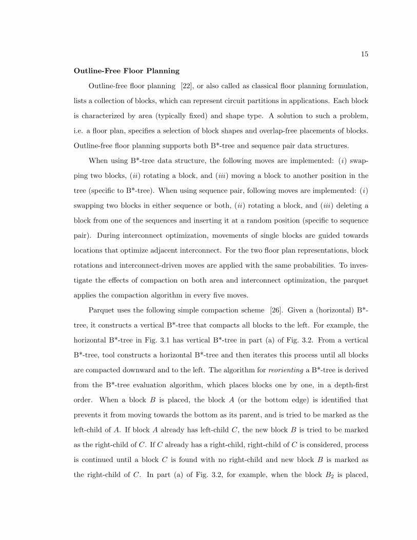
3.2.1 Parquet Floor Planner
Parquet is software for floor planning based on simulated annealing [21]. It has been
developed by the university of Michigan. It has been used in a number of projects in
computer-aided design and computer architecture. While originally designed for fixed-
outline floor planning using sequence pairs data structure, it can also be applied to classical
min-area block packing. The internal floor plan representation alternates between sequence
pairs and B*-Trees data structures. There are many different types of floor planning. But
Parquet supports two important types of floor planning: outline-free floor planning and
fixed outline floor planning.
15
Outline-Free Floor Planning
Outline-free floor planning [22], or also called as classical floor planning formulation,
lists a collection of blocks, which can represent circuit partitions in applications. Each block
is characterized by area (typically fixed) and shape type. A solution to such a problem,
i.e. a floor plan, specifies a selection of block shapes and overlap-free placements of blocks.
Outline-free floor planning supports both B*-tree and sequence pair data structures.
When using B*-tree data structure, the following moves are implemented: (i) swap-
ping two blocks, (ii) rotating a block, and (iii) moving a block to another position in the
tree (specific to B*-tree). When using sequence pair, following moves are implemented: (i)
swapping two blocks in either sequence or both, (ii) rotating a block, and (iii) deleting a
block from one of the sequences and inserting it at a random position (specific to sequence
pair). During interconnect optimization, movements of single blocks are guided towards
locations that optimize adjacent interconnect. For the two floor plan representations, block
rotations and interconnect-driven moves are applied with the same probabilities. To inves-
tigate the effects of compaction on both area and interconnect optimization, the parquet
applies the compaction algorithm in every five moves.
Parquet uses the following simple compaction scheme [26]. Given a (horizontal) B*-
tree, it constructs a vertical B*-tree that compacts all blocks to the left. For example, the
horizontal B*-tree in Fig. 3.1 has vertical B*-tree in part (a) of Fig. 3.2. From a vertical
B*-tree, tool constructs a horizontal B*-tree and then iterates this process until all blocks
are compacted downward and to the left. The algorithm for reorienting a B*-tree is derived
from the B*-tree evaluation algorithm, which places blocks one by one, in a depth-first
order. When a block B is placed, the block A (or the bottom edge) is identified that
prevents it from moving towards the bottom as its parent, and is tried to be marked as the
left-child of A. If block A already has left-child C, the new block B is tried to be marked
as the right-child of C. If C already has a right-child, right-child of C is considered, process
is continued until a block C is found with no right-child and new block B is marked as
the right-child of C. In part (a) of Fig. 3.2, for example, when the block B2 is placed,
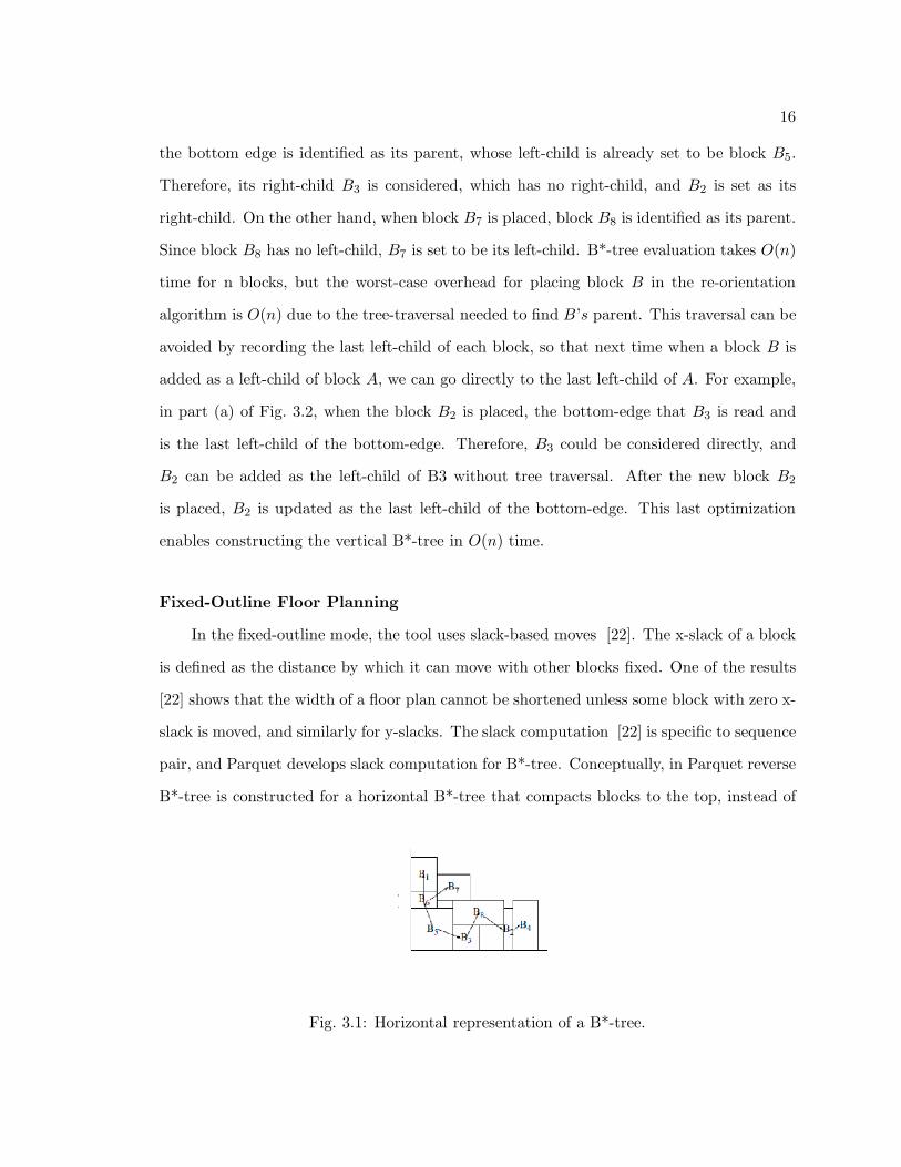
16
the bottom edge is identified as its parent, whose left-child is already set to be block B5.
Therefore, its right-child B3 is considered, which has no right-child, and B2 is set as its
right-child. On the other hand, when block B7 is placed, block B8 is identified as its parent.
Since block B8 has no left-child, B7 is set to be its left-child. B*-tree evaluation takes O(n)
time for n blocks, but the worst-case overhead for placing block B in the re-orientation
algorithm is O(n) due to the tree-traversal needed to find B’s parent. This traversal can be
avoided by recording the last left-child of each block, so that next time when a block B is
added as a left-child of block A, we can go directly to the last left-child of A. For example,
in part (a) of Fig. 3.2, when the block B2 is placed, the bottom-edge that B3 is read and
is the last left-child of the bottom-edge. Therefore, B3 could be considered directly, and
B2 can be added as the left-child of B3 without tree traversal. After the new block B2
is placed, B2 is updated as the last left-child of the bottom-edge. This last optimization
enables constructing the vertical B*-tree in O(n) time.
Fixed-Outline Floor Planning
In the fixed-outline mode, the tool uses slack-based moves [22]. The x-slack of a block
is defined as the distance by which it can move with other blocks fixed. One of the results
[22] shows that the width of a floor plan cannot be shortened unless some block with zero x-
slack is moved, and similarly for y-slacks. The slack computation [22] is specific to sequence
pair, and Parquet develops slack computation for B*-tree. Conceptually, in Parquet reverse
B*-tree is constructed for a horizontal B*-tree that compacts blocks to the top, instead of
Fig. 3.1: Horizontal representation of a B*-tree.
17
the bottom (part (b) of Fig. 3.2). The y-slack is the difference in y-coordinates of each
block in these two horizontal B*-tree. To evaluate the x-slacks, the vertical B*-tree T is
first constructed that compacts blocks to the left. Then the reverse vertical B*-tree T ’ is
constructed from T that compacts blocks to the right (part (c) of Fig. 3.2). The difference
in x-coordinates of each block in T ’ and the original horizontal B*-tree is its x-slack. The
slack computation for B*-tree takes O(n) time. This allows slack-based moves to be made
identical for B*-tree and sequence pair.
3.2.2 Simulated Annealing
Simulated annealing is a technique to find a good solution to an optimization problem
by trying random variations of the current solution [27]. A worse variation is accepted as
the new solution with a probability that decreases as the computation proceeds. The slower
the cooling schedule or rate of decrease, the more likely the algorithm is to find an optimal
or near-optimal solution.
This technique stems from thermal annealing which aims to obtain perfect crystalliza-
tions by a slow enough temperature reduction to give atoms the time to attain the lowest
energy state.
The search inside simulated annealing tries to avoid local minima by jumping out of
them early in the computation. Towards the end of the computation, when the temperature
Fig. 3.2: (a) Shows the vertical B*-tree of the horizontal B*-tree in Fig. 3.1. (b) Showsthe reverse horizontal B*-tree of the B*-tree in Fig. 3.1. All blocks are packed to the topinstead of the bottom. (c) Shows the reverse vertical B*-tree of the vertical B*- tree in (a).
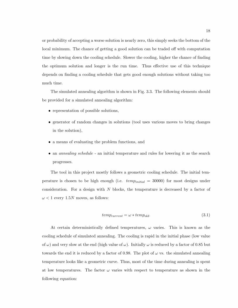
18
or probability of accepting a worse solution is nearly zero, this simply seeks the bottom of the
local minimum. The chance of getting a good solution can be traded off with computation
time by slowing down the cooling schedule. Slower the cooling, higher the chance of finding
the optimum solution and longer is the run time. Thus effective use of this technique
depends on finding a cooling schedule that gets good enough solutions without taking too
much time.
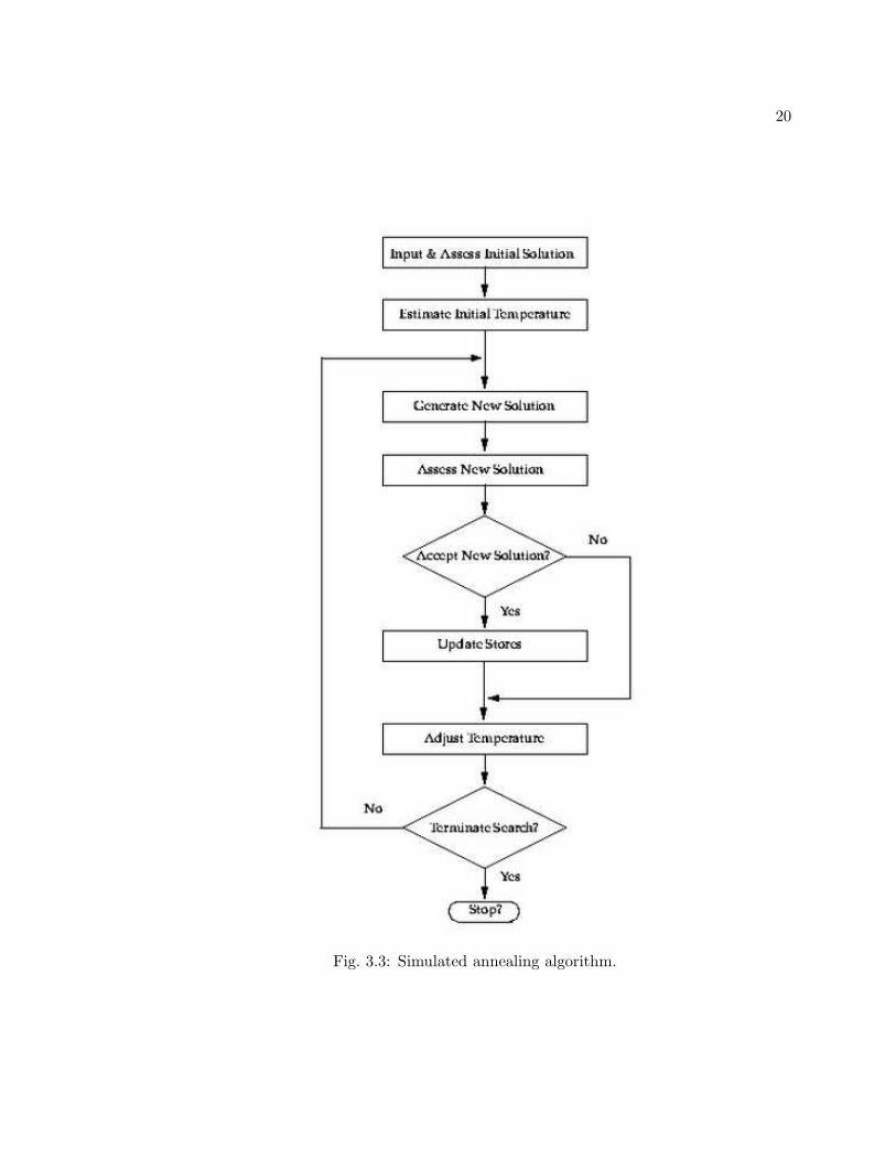
The simulated annealing algorithm is shown in Fig. 3.3. The following elements should
be provided for a simulated annealing algorithm:
• representation of possible solutions,
• generator of random changes in solutions (tool uses various moves to bring changes
in the solution),
• a means of evaluating the problem functions, and
• an annealing schedule - an initial temperature and rules for lowering it as the search
progresses.
The tool in this project mostly follows a geometric cooling schedule. The initial tem-
perature is chosen to be high enough (i.e. tempinitial = 30000) for most designs under
consideration. For a design with N blocks, the temperature is decreased by a factor of
ω < 1 every 1.5N moves, as follows:
tempcurrent = ω ∗ tempold. (3.1)
At certain deterministically defined temperatures, ω varies. This is known as the
cooling schedule of simulated annealing. The cooling is rapid in the initial phase (low value
of ω) and very slow at the end (high value of ω). Initially ω is reduced by a factor of 0.85 but
towards the end it is reduced by a factor of 0.98. The plot of ω vs. the simulated annealing
temperature looks like a geometric curve. Thus, most of the time during annealing is spent
at low temperatures. The factor ω varies with respect to temperature as shown in the
following equation:
19
ω = 0.85//30000(tempinitial ) < tempcurrent < 2000
= 0.90//2000 < tempcurrent < 1000
= 0.95//1000 < tempcurrent < 500
= 0.96//500 < tempcurrent < 200
= 0.80//200 < tempcurrent < 10
= 0.98//10 < tempcurrent < 0.1(tempcool).
There is also an option to run the annealer for a specified length of time. In this mode
the temperature schedule remains the same but the number of moves between each iteration
changes.
3.2.3 Objective Function for Simulated Annealing
The objective function for the thermal aware floor planning using the simulated an-
nealing routine is shown below:
∆ =CA + CAR
2∗ A +
CW + CAR
2∗ W + CT ∗ T, (3.2)
where CA, CW , and CT are the weights of area, the wire length, and the maximum tem-
perature, respectively. CAR is the aspect ratio weight. Its value is kept constant at 0.2.
The sum of CAR, CA, CW , and CT should always be equal to 1.0. CT has a positive sign
because the maximum temperature T needs to be minimized.
The problem with the above objective function is that each of the terms - area, wire
length, and temperature is measured in different units. Hence to obtain a linear objective
function, we normalize each term of the objective function. Normalization is done as shown
below:
∆A =(tempArea − currArea) ∗ 1.2 ∗ timeInit
currArea, (3.3)
20
Fig. 3.3: Simulated annealing algorithm.
21
∆W =(tempHPWL − currHPWL) ∗ 1.2 ∗ timeInit
currHPWL, (3.4)
∆T =(tempMaxTemp − currMaxTemp) ∗ 1.2 ∗ timeInit
currMaxTemp, (3.5)
where ∆A, ∆W , ∆T are the normalized area, wire length, and maximum temperature, re-
spectively; currArea, currHPWL, currMaxTemp are the area, wire length, and maximum
temperature, respectively, of the current solution; tempArea, tempHPWL, tempMaxTemp
are the area, wirelength, and maximum temperature, respectively, of the modified (next)
solution; timeInit is the initial temperature of the cooling schedule.
Now the modified objective function becomes:
∆ =CA + CAR
2∗ ∆A +
CW + CAR
2∗ ∆W + CT ∗ ∆T. (3.6)
During the annealing, all moves with a negative ∆ are accepted. Negative ∆ implies
an improvement over the previous solution. All moves with a positive ∆ are accepted if
random < exp (−∆∗tempinitial
tempcurrent), where random is a random number between 0 and 1. Thus,
the probability of accepting a bad move decreases as tempcurrent is reduced.
3.2.4 HotSpot Thermal Modeling Tool
HotSpot tool has been developed by University of Virginia. HotSpot is an accurate and
fast thermal modeling tool suitable for use in architectural studies. For every input floor
plan, HotSpot generates an equivalent circuit of thermal resistances and capacitances. The
equivalent circuit of thermal resistances and capacitances corresponds to microarchitecture
blocks and essential aspects of the thermal package. HotSpot has a simple set of interfaces.
The main advantage of HotSpot is its compatibility with the kinds of power/performance
models used in the computer-architecture community. It does not require detailed design
or synthesis description. It makes it possible to study thermal evolution over long periods
of real, full-length applications.
In this project, the tool uses HotSpot tool to calculate the maximum temperature
amongst all the blocks in the floor plan. The maximum temperature thus calculated is
22
used in the objective function of the simulated annealing routine inside the Parquet floor
planner. The tool has integrated the source code of HotSpot 5.0 into the source code
of Parquet 4.5. Source code of both HotSpot, as well as Parquet, have been altered to
facilitate the interfacing. Especially, the data structures of Parquet have been modified
to accommodate an extra temperature factor. Also, the definitions of several classes and
member functions have also been modified. Section 3.3 talks more about the tool execution
flow and the interfacing between HotSpot and Parquet.
There are several models of HotSpot that could be used for temperature calculation [28].
But the tool makes use of the block model. Block model (also called the base model) is
the simplest and fastest method of temperature calculation. The thermal model is bundled
as a trace-level simulator that takes a power trace file and a floor plan file as inputs and
outputs the corresponding transient temperatures onto a temperature trace file. But instead
of generating a temperature trace output, the tool has been modified to be a function
which gets invoked inside the simulated annealing routine of the Parquet floor planner.
The function takes a power trace file and a floor plan file (generated by parquet every
iteration) as arguments and returns the maximum temperature of the floor plan. Maximum
temperature thus calculated is used in the objective function of the annealing process. The
function prototype is shown below:
double hotspot parquet(char ∗ conf, char ∗ conf value, char ∗ file f lp, char ∗
file f lp name, char∗ file ptrace, char∗ file ptrace name, char∗ file output, char∗
file output name, char ∗ file steadystate, char ∗ file steadystate name, char ∗
file initial, char ∗ file initial name)
As shown above, along with floor plan file (file f lp name) and power file (file ptrace),
function also takes a configuration file. The configuration file consists of the thermal model
parameters, heat sink specifications, heat spreader specifications, interface material speci-
fications, etc. These parameters and specifications are used by HotSpot to build a thermal
model consisting of thermal resistances and capacitances.
23
3.3 Interfacing of HotSpot and Parquet
Interfacing of HotSpot and Parquet is shown in Fig. 3.4. As shown, HotSpot gets called
during all the iterations of the simulated annealing routine inside Parquet. Every time a new
solution is generated, area, wire length, and temperature (using HotSpot) are calculated.
Optimization is done using the objective function as shown in the above sections.
Parquet takes a floor plan in the form of blocks/net/pl files. The blocks/net/pl are
the industry standard formats in benchmarks like GSRC and MCNC for providing floor
plan information. The blocks file consists of the list of all the blocks in the floor plan. It
provides the name of the blocks, type of the blocks (hardrectilinear/softrectilinear), size of
the blocks, and names of all the terminals on the blocks. The net and pl files provide the
information related to the interconnects available in the floor plan, how they are connected,
and where they are connected.
Parquet reads these files and extracts the blocks’ dimensions and other placement
information from these files. It creates the data structures (DB,Nodes,Node) to hold all
the information relevant to the floor plan. The data structures of the Parquet have been
modified in this project to contain information related to temperature. Extra data members
have been added. Constructors have been modified and member functions have been added
to access these extra data members. After the construction of the data structures, Parquet
selects either B*-trees or sequence pairs to carry out the floor planning process and the
corresponding annealer is called. During each iteration of the simulated annealing, area,
wire length, and maximum temperature of the chip is calculated and optimization is done.
For the calculation of temperature HotSpot is called during every iteration.
In order to calculate the temperature, HotSpot takes a floor plan in the form of flp file.
This flp format is completely different than the input format of the Parquet. The tool writes
the floor plan information taken from the Parquet data structures to the flp file every time
a new solution is generated. Modified HotSpot returns the maximum temperature which is
stored in the data structures of Parquet and used later for the optimization using simulated
annealing.
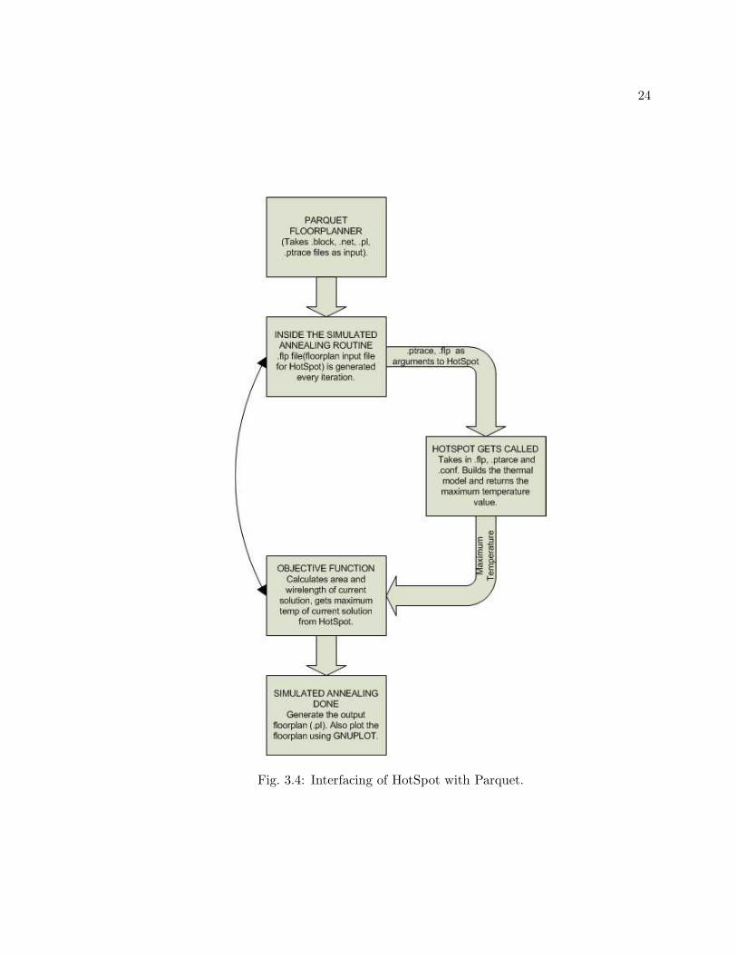
24
Fig. 3.4: Interfacing of HotSpot with Parquet.
25
Chapter 4
Results
4.1 Generation of Ptrace File
Floor plan of every microprocessor is divided into several soft/hard rectilinear blocks.
The thermal aware floor planning tool takes the floor plan as input in the form of blocks/net/pl
files. These blocks/net/pl files are taken from the MCNC [29] and GSRC benchmarks [30].
MCNC and GSRC benchmarks are the industry standard bechmarks used in VLSI/CAD
testing. The tool also requires the ptrace (power trace) file along with other input files.
But the MCNC and GSRC benchmarks available with Parquet do not provide the ptrace
file. So the ptrace file was generated manually using random number generator as described
below (please refer to Fig. 4.1 for the format of the ptrace file).
First, Parquet software was modified to write down the block names into the ptrace
file. Each block in the ptrace file has 100 power numbers listed below it. A random number
generator was used to generate these power numbers. The power numbers were generated
such that few of the blocks have high-power numbers, few of them have power numbers
in the medium range and few of them have low-power numbers. The high, medium, and
low ranges depend entirely on the arrangement of blocks in a floor plan and the sizes of
blocks in a floor plan. For example, hp benchmark used to test the tool has blocks with
power numbers around 3.5 for the high range while apte benchmark has blocks with power
numbers around 9.0 for the high range. The ranges for each of the benchmark were found
out experimentally by running the tool multiple times for different values of power numbers.
The temperature profile was generated for each run and the power numbers giving the best
profile were selected. The ptrace file thus generated was used along with the other input
files to perform thermal aware floor planning.
26
Idea of thermal aware floor planning tool is to arrange the blocks in a floor plan such
that maximum temperature of the floor plan is reduced. The high-power blocks are the
most likely cause of generating high temperature. Also if two or more high power blocks
come near to each other, they might create a Hotspot and would result in high temperatures
for all of them. In order to reduce the maximum temperature of the floor plan, the blocks
with high-power numbers should be placed away from each other as far as possible. So
that high power blocks would dissipate heat to the low-power blocks. And the result would
be reduced maximum temperature. To test this concept, the power numbers of few blocks
in the floor plan are set to a high value (high range blocks) to test how these high-power
blocks are placed in the floor plan. It was found out that the blocks with high-power values
were placed as far away from each other as possible. The following sections would talk in
more detail about it.
4.2 Testing
The tool was run several times on a CentOS linux machine with Intel Core2 (2.83 GHz)
CPU and 4GB RAM. The MCNC benchmarks - hp, xerox, apte, ami − 33, and ami − 49,
and the GSRC benchmarks - n10, n30, and n50 were used to test the correctness of the
tool. Each of the benchmarks was run several times and the best result was selected.
The input blocks/net/pl files and the randomly generated experimentally tested ptrace
file (refer Sec. 4.1) were taken as input. The thermal aware floor planner was run first with
thermal coefficient set to 0.0 (floor planning without the temperature part of the objective
function; AreaWeight: 0.4, WireWeight: 0.4, TempWeight: 0.0, and ARWeight: 0.2) and
Fig. 4.1: Example of a ptrace file.
27
then later with thermal coefficient set to 0.3 (floor planning with the temperature part of the
objective function; AreaWeight: 0.3, WireWeight: 0.2, TempWeight: 0.3, and ARWeight:
0.2). Both the cases were run multiple times and the best results were selected and compared
with each other. It was found out that adding a temperature factor to the objective function
does not affect the floor planning process as a whole. This is because essentially the blocks
in the floor plan generated by thermal aware floor planner are the same as the blocks in
floor plan generated by a regular floor planner. Only the arrangement is changed. Also the
slack-based moves executed by Parquet and the compaction algorithm used by it make sure
that the blocks are placed very close to each other. In fact, the maximum temperature of
the floor plan was reduced significantly with only slight increase in area and wire length.
Thus, thermal aware floor planning can be used as one of the effective methods to reduce
the maximum temperature inside the processor. Please refer to following section (Sec. 4.3)
for more detailed results.
4.3 Results Obtained From the Tool
As described above, the thermal aware floor planning tool was run for two cases: (i)
without considering the temperature part of the objective function (just like normal Parquet
floor planning), (ii) considering the temperature part of the objective function (thermal
aware floor planning). The results of the two cases were compared with each other in terms
of three main parameters: area, wire length, and temperature. The tool was run for multiple
times for MCNC benchmarks like hp, xerox, apte, ami− 33, and ami− 49, and the GSRC
benchmarks like n10, n30, and n50. The effects of the thermal aware floor planning on
temperature, area, and wire length are described in subsections below.
4.3.1 Effect of Thermal Aware Floor Planning on Temperature
As shown in Fig. 4.2 and Fig. 4.3, the maximum temperature of the chip reduces
considerably when thermal aware floor planning is used, in comparison to normal floor
planning or floor planning without temperature factor. Figure 4.2 shows the normalized
reduction of maximum chip temperature in various benchmarks. Figure 4.3 shows the
28
percentage reduction of maximum chip temperature. About 5-20% reduction (see Fig. 4.3)
in maximum temperature of chip was noticed when thermal aware floor planner was run. In
apte benchmark, temperature of the floor plan after thermal aware floor planning was 30◦C
or approximately 18% less than the temperature of the floor plan after normal floor planning.
In hp benchmark, the temperature reduced by 19◦C or rougly 17%. The temperature
reduction is completely dependent on the variation in the power densities of the blocks. If
all the blocks in the floor plan have power densities in the same range, there is hardly any
reduction seen in temperature. Whereas, if there is a large variation in power densities of the
blocks, hot blocks could be placed besides cooler blocks and better temperature reduction
would be obtained. Increase in area can also be a cause of temperature reduction. But
as shown in next subsection, the area overhead noted after thermal aware floor planning is
about 5% or less in most cases. Thus, area overhead has a minimal effect on temperature
reduction and it occurs mainly because of the placement of blocks.
4.3.2 Effect of Thermal Aware Floor Planning on Area of the Chip
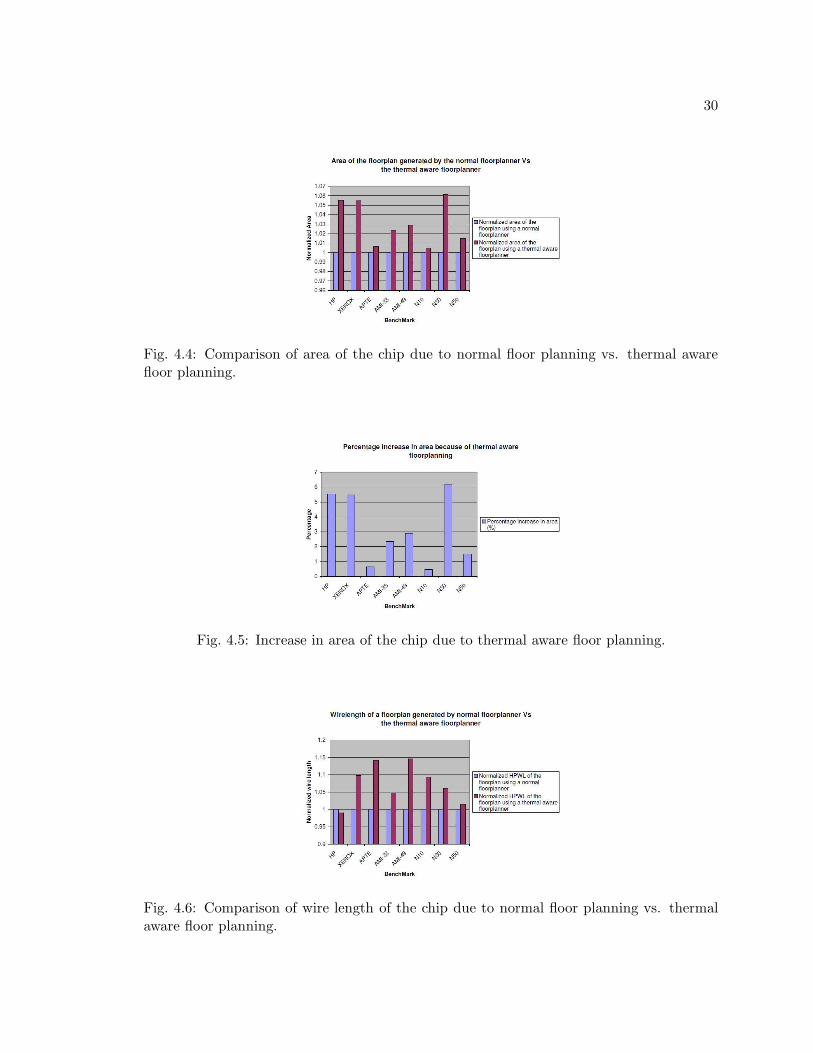
Figure 4.4 shows the normalized increase in chip area in various benchmarks. Figure 4.5
shows the percentage increase in chip area. As a result of thermal aware floor planning,
there is a slight increase in chip area. In most of the cases (as shown in Fig. 4.5), the
increase is area is below 5%. In benchmarks, like ami − 49, the increase in chip area was
found as low as 0.5%. Thus, the effect of thermal aware floor planning on chip area was
Fig. 4.2: Comparison of maximum temperature of the chip due to normal floor planningvs. thermal aware floor planning.
29
found to be minimal in most of the benchmarks. Hence, the temperature reduction is a
result of placement of blocks in a thermal aware manner rather than the increase in area.
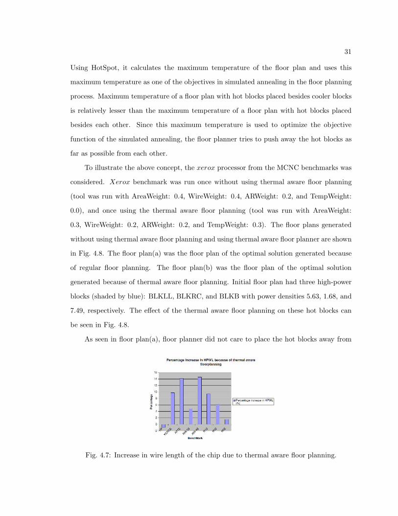
4.3.3 Effect of Thermal Aware Floor Planning on Wire Length
Increase in chip area causes a slight increase in wire length of the chip. Figure 4.6 shows
the normalized increase in wire length in various benchmarks due to thermal aware floor
planning. Figure 4.7 shows the percentage increase in wire length due to thermal aware
floor planning. In most cases, increase in wire length was less than 10% of the original wire
length. In one or two cases though, increase in wire length was noted around 14%. In few
cases, wire length noted was as low as 1% as well. Thus, there is no significant increase in
wire length as a result of thermal aware floor planning.
In hp benchmark, sometimes a small reduction in wire length was observed. The floor
plans in both the cases were plotted and it was noticed that the reduction in wire length
was because of rotation of few blocks who had interconnects between them.
4.3.4 Effect of Thermal Aware Floor Planning on the Placement of the Blocks
As described in Sec. 1.2 cooling of the blocks in a floor plan happens due to lateral
spreading of heat through silicon blocks [10]. If a hot block is placed besides cooler blocks,
lateral spreading of heat takes place. As a result, the temperature of the hot block is
reduced. Thermal aware floor planning tool uses this concept of lateral heat diffusion.
Fig. 4.3: Reduction in maximum temperature of the chip due to thermal aware floor plan-ning.
30
Fig. 4.4: Comparison of area of the chip due to normal floor planning vs. thermal awarefloor planning.
Fig. 4.5: Increase in area of the chip due to thermal aware floor planning.
Fig. 4.6: Comparison of wire length of the chip due to normal floor planning vs. thermalaware floor planning.
31
Using HotSpot, it calculates the maximum temperature of the floor plan and uses this
maximum temperature as one of the objectives in simulated annealing in the floor planning
process. Maximum temperature of a floor plan with hot blocks placed besides cooler blocks
is relatively lesser than the maximum temperature of a floor plan with hot blocks placed
besides each other. Since this maximum temperature is used to optimize the objective
function of the simulated annealing, the floor planner tries to push away the hot blocks as
far as possible from each other.
To illustrate the above concept, the xerox processor from the MCNC benchmarks was
considered. Xerox benchmark was run once without using thermal aware floor planning
(tool was run with AreaWeight: 0.4, WireWeight: 0.4, ARWeight: 0.2, and TempWeight:
0.0), and once using the thermal aware floor planning (tool was run with AreaWeight:
0.3, WireWeight: 0.2, ARWeight: 0.2, and TempWeight: 0.3). The floor plans generated
without using thermal aware floor planning and using thermal aware floor planner are shown
in Fig. 4.8. The floor plan(a) was the floor plan of the optimal solution generated because
of regular floor planning. The floor plan(b) was the floor plan of the optimal solution
generated because of thermal aware floor planning. Initial floor plan had three high-power
blocks (shaded by blue): BLKLL, BLKRC, and BLKB with power densities 5.63, 1.68, and
7.49, respectively. The effect of the thermal aware floor planning on these hot blocks can
be seen in Fig. 4.8.
As seen in floor plan(a), floor planner did not care to place the hot blocks away from
Fig. 4.7: Increase in wire length of the chip due to thermal aware floor planning.
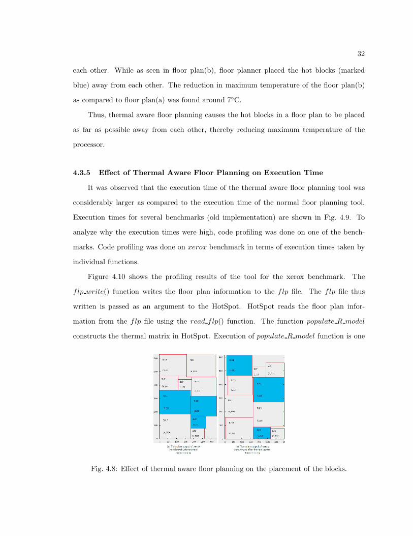
32
each other. While as seen in floor plan(b), floor planner placed the hot blocks (marked
blue) away from each other. The reduction in maximum temperature of the floor plan(b)
as compared to floor plan(a) was found around 7◦C.
Thus, thermal aware floor planning causes the hot blocks in a floor plan to be placed
as far as possible away from each other, thereby reducing maximum temperature of the
processor.
4.3.5 Effect of Thermal Aware Floor Planning on Execution Time
It was observed that the execution time of the thermal aware floor planning tool was
considerably larger as compared to the execution time of the normal floor planning tool.
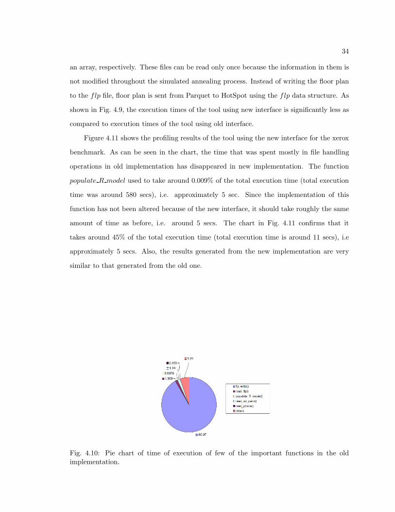
Execution times for several benchmarks (old implementation) are shown in Fig. 4.9. To
analyze why the execution times were high, code profiling was done on one of the bench-
marks. Code profiling was done on xerox benchmark in terms of execution times taken by
individual functions.
Figure 4.10 shows the profiling results of the tool for the xerox benchmark. The
flp write() function writes the floor plan information to the flp file. The flp file thus
written is passed as an argument to the HotSpot. HotSpot reads the floor plan infor-
mation from the flp file using the read flp() function. The function populate R model
constructs the thermal matrix in HotSpot. Execution of populate R model function is one
Fig. 4.8: Effect of thermal aware floor planning on the placement of the blocks.
33
of the important steps in the temperature calculation process in HotSpot. The function
read str pairs() reads the config file while the function read ptrace reads the power trace
file. The functions that perform simulated annealing, area and wire length estimation, etc.
are listed under the category others in the pie chart.
As seen in the pie chart in Fig. 4.10, the function flp write takes the maximum amount
of time. This is because, for every move in the simulated annealing, HotSpot is called twice.
And for every call to HotSpot, floor plan information is sent from Parquet to HotSpot
using the flp file, which is written using flp write. Also, flp write makes use of standard
templates library feature of C++ language to write to the flp file, which increases the time
of execution even more. Also, the functions like read str pairs, read flp and read ptrace
take considerable amount of time to execute because the config, the flp, and the ptrace
files are opened and read every single time there is a call to HotSpot.
Thus, in order to decrease the exection time, the interface between the Parquet and
HotSpot was implemented again without the time consuming file handling operations.
4.4 New Implementation of the Interface Between Parquet and HotSpot
The execution time of the tool using the old interface was significantly high because
the tool used to perform several file handling operations for every move made inside the
simulated annealing. In order to reduce the execution time, the new iterface between
Parquet and HotSpot avoids using file handling operations. The config and the ptrace files
are read only once before the start of the simulated annealing and stored in a hash table and
Fig. 4.9: Table of execution times for several benchmarks using for both old and newimplementations of the interface between HotSpot and Parquet.
34
an array, respectively. These files can be read only once because the information in them is
not modified throughout the simulated annealing process. Instead of writing the floor plan
to the flp file, floor plan is sent from Parquet to HotSpot using the flp data structure. As
shown in Fig. 4.9, the execution times of the tool using new interface is significantly less as
compared to execution times of the tool using old interface.
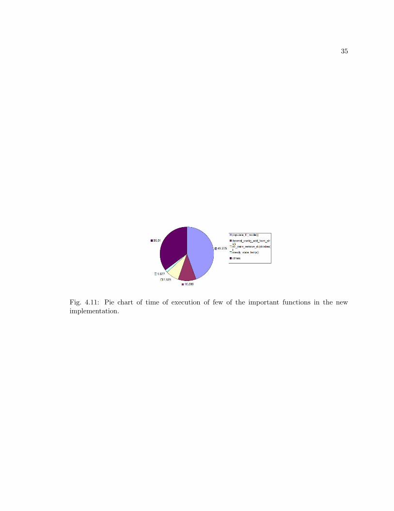
Figure 4.11 shows the profiling results of the tool using the new interface for the xerox
benchmark. As can be seen in the chart, the time that was spent mostly in file handling
operations in old implementation has disappeared in new implementation. The function
populate R model used to take around 0.009% of the total execution time (total execution
time was around 580 secs), i.e. approximately 5 sec. Since the implementation of this
function has not been altered because of the new interface, it should take roughly the same
amount of time as before, i.e. around 5 secs. The chart in Fig. 4.11 confirms that it
takes around 45% of the total execution time (total execution time is around 11 secs), i.e
approximately 5 secs. Also, the results generated from the new implementation are very
similar to that generated from the old one.
Fig. 4.10: Pie chart of time of execution of few of the important functions in the oldimplementation.
35
Fig. 4.11: Pie chart of time of execution of few of the important functions in the newimplementation.
36
Chapter 5
Conclusion and Future Work
This project develops a tool that helps in temperature reduction of a chip through
temperature aware floor planning. Through experiments on various microprocessors in-
cluded in the MCNC and GSRC benchmarks, it has been shown that by using the thermal
aware tool, temperature reduction of about 5-20% can be achieved as compared to normal
floor planning tool. In benchmarks like Apte, almost 30◦C temperature reduction can be
acheived using this tool. On the other hand, the penalty on area of the chip is less than
5% in most cases. In few cases it is as low as 0.5% which is as good as negligible. Also, the
penalty on wire length was as less as 14%. In most cases the wire length penalty was found
less than 10%. In future designs based on deep sub-micron technology, chip temperatures
are expected to rise further, making the advantages of thermal aware floor planning even
more prominent.
Execution time can be reduced even more by making use of optimization techniques.
One of the methods that can be used is adding math accelaration package to HotSpot. Math
acceleration would help HotSpot to construct a thermal matrix at a faster pace, thereby
reducing the execution time of the tool.
Tool can also be modified and used in 3D-IC design flow (3D-thermal aware floor
planner). Research is going on in that area. Hung et al. [31] have developed one such
implementation of 3D-thermal aware floor planner.
37
References
[1] R. Schaller, “Moore’s law: past, present and future,” Spectrum, IEEE, vol. 34, pp.52–59, 1997.
[2] S. Borkar, “Design challenges of technology scaling,” Micro, IEEE, vol. 19, 1999.
[3] “Intel tries to keep it cool,” Available: [Online][http://www.pcworld.idg.com.au/article/108386/intel tries keep its cool/], 2004.
[4] “Electrothermal monte carlo modelling of submicron hfets,” Available: [Online][http://www.nanofolio.org/research/paper03.php], 2004.
[5] S. Gunther, F. Binns, D. M. Carmean, and J. C. Hall, “Managing the impact ofincreasing microprocessor power consumption,” Intel Technology Journal, vol. 5, 2001.
[6] P. Lall, “Temperature as an input to microelectronics-reliability models,” IEEE Trans-actions on Reliability, vol. 53, p. 3, 1996.
[7] Y. Liu, R. P. Dick, L. Shang, and H. Yang, “Accurate temperature-dependent in-tegrated circuit leakage power estimation is easy,” in DATE ’07: Proceedings of theConference on Design, Automation and Test in Europe, pp. 1526–1531, 2007.
[8] K. Skadron, M. Stan, W. Huang, S. Velusamy, K. Sankaranarayanan, and D. Tarjan,“Temperature-aware microarchitecture,” ISCA ’03: 30th Annual International Sym-posium on Computer Architecture, 2003.
[9] S. M. Sait and Y. H., VLSI Physical Design Automation. Danvers, MA: World Sci-entific, 1999.
[10] K. Skadron, M. Stan, S. Velusamy, and K. Sankaranarayanan, “A case for thermal-aware floor planning at the microarchitectural level,” Journal of Instruction-Level Par-allelism 8, 2005.
[11] K. Skadron, M. Stan, W. Huang, S. Velusamy, K. Sankaranarayanan, and D. Tarjan,“Temperature-aware microarchitecture: Modeling and implementation,” Associationfor Computing Machinery Transactions on Architecture and Code Optimization, vol. 1,p. 94, 2004.
[12] “Hotspot,” Available: [Online] [http://lava.cs.virginia.edu/hotspot], 2010.
[13] W. Huang, M. Stan, M. R. Skadron, K. Sankaranarayanan, K. Ghosh, and S. Velusamy,“Compact thermal modeling for temperature-aware design,” Design Automation Con-ference, vol. 41, pp. 878–883, 2004.
[14] P. Chaparro, J. Gonzalez, and A. Gonzalez, “Thermal-aware clustered microarchitec-tures,” ICCD ’04: IEEE Transactions on Computer Design: VLSI in Computers andProcessors, pp. 48–53, 2004.
38
[15] C. N. Chu and D. F. Wong, “A matrix synthesis approach to thermal placement,” IEEETransactions on Computer Aided Design of Integrated Circuits and Systems, vol. 11,pp. 1166–1174, 1998.
[16] J. Donald and M. Martonosi, “Temperature-aware design issues for smt and cmp ar-chitectures,” In Proceedings of the Workshop on Complexity-Effective Design, pp.113–123, 2004.
[17] Y. Li, K. Skadron, Z. Hu, and D. Brooks, “Evaluating the thermal efficiency of smtand cmp architectures,” In IBM T. J. Watson Conference on Interaction betweenArchitecture, Circuits, and Compilers, 2004.
[18] W.-L. Hung, Y. Xie, N. Vijaykrishnan, C. Addo-Quaye, T. Theocharides, and M. Irwin,“Thermal-aware floor planning using genetic algorithms,” IEEE International Sympo-sium on Quality Electronic Design, p. 634, 2005.
[19] W.-L. Hung, C. Addo-Quaye, T. Theocharides, Y. Xie, N. Vijaykrishnan, and M. J.Irwin, “Thermal-aware ip virtualization and placement for networks-on-chip architec-ture,” ICCD ’04: IEEE International Conference on Computer Design: VLSI in Com-puters and Processors, p. 430, 2004.
[20] Y. Han, I. Koren, and C. A. Moritz, “Temperature aware floor planning,” Workshopon Temperature Aware Microarchitectures, 2005.
[21] “Parquet,” Available: [Online] [http://vlsicad.eecs.umich.edu/BK/parquet/], 2006.
[22] S. Adya and I. Markov, “Fixed-outline floor planning: enabling hierarchical design,”IEEE Transactions on Very Large Scale Integration (VLSI) Systems, vol. 11, pp. 1120–1135, 2003.
[23] S. Adya and I. Markov, “Fixed-outline floor planning through better local search,”Proceedings of the IEEE Transactions on Computer Design, pp. 328–334, 2001.
[24] H. Murata, K. Fujiyoshi, S. Nakatake, and Y. Kajitani, “Vlsi module placement basedon rectangle-packing by the sequence-pair,” IEEE Transactions on Computer-AidedDesign of Integrated Circuits and Systems, vol. 15, pp. 1518–1524, 1996.
[25] Y.-C. Chang, Y.-W. Chang, G.-M. Wu, and S.-W. Wu, “B*-trees: a new representa-tion for non-slicing floor plans,” in DAC ’00: Proceedings of the 37th Annual DesignAutomation Conference, pp. 458–463, 2000.
[26] H. H. Chan, S. N. Adya, and I. L. Markov, “Are floor plan representations important indigital design?” in ISPD ’05: Proceedings of the International Symposium on PhysicalDesign, pp. 129–136, 2005.
[27] S. Kirkpatrick, “Optimization by simulated annealing: Quantitative studies,” Journalof Statistical Physics, vol. 34, pp. 975–986, 1983.
[28] “Hotspot-howto,” Available: [Online] [http://lava.cs.virginia.edu/HotSpot/HotSpot-HOWTO.htm], 2010.
39
[29] “Mcnc-benchmark,” Available: [Online] [http://vlsicad.eecs.umich.edu/BK/MCNCbench/], 2006.
[30] “Gsrc-benchmark,” Available: [Online] [http://vlsicad.eecs.umich.edu/BK/GSRCbench/], 2006.
[31] W. L. Hung, G. Link, Y. Xie, N. Vijaykrishnan, and M. Irwin, “Interconnect andthermal-aware floor planning for 3d microprocessors,” ISQED ’06: 7th InternationalSymposium on Quality Electronic Design,, p. 6, 2006.

40
Appendix
41
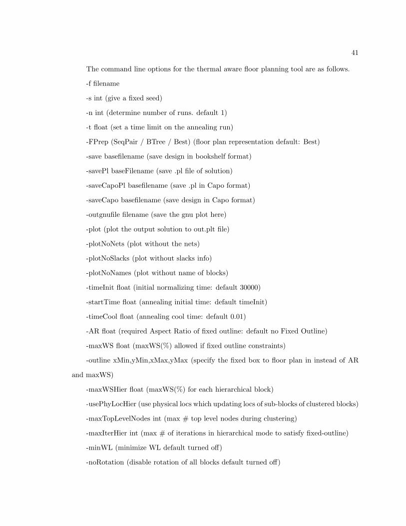
The command line options for the thermal aware floor planning tool are as follows.
-f filename
-s int (give a fixed seed)
-n int (determine number of runs. default 1)
-t float (set a time limit on the annealing run)
-FPrep (SeqPair / BTree / Best) (floor plan representation default: Best)
-save basefilename (save design in bookshelf format)
-savePl baseFilename (save .pl file of solution)
-saveCapoPl basefilename (save .pl in Capo format)
-saveCapo basefilename (save design in Capo format)
-outgnufile filename (save the gnu plot here)
-plot (plot the output solution to out.plt file)
-plotNoNets (plot without the nets)
-plotNoSlacks (plot without slacks info)
-plotNoNames (plot without name of blocks)
-timeInit float (initial normalizing time: default 30000)
-startTime float (annealing initial time: default timeInit)
-timeCool float (annealing cool time: default 0.01)
-AR float (required Aspect Ratio of fixed outline: default no Fixed Outline)
-maxWS float (maxWS(%) allowed if fixed outline constraints)
-outline xMin,yMin,xMax,yMax (specify the fixed box to floor plan in instead of AR
and maxWS)
-maxWSHier float (maxWS(%) for each hierarchical block)
-usePhyLocHier (use physical locs which updating locs of sub-blocks of clustered blocks)
-maxTopLevelNodes int (max # top level nodes during clustering)
-maxIterHier int (max # of iterations in hierarchical mode to satisfy fixed-outline)
-minWL (minimize WL default turned off)
-noRotation (disable rotation of all blocks default turned off)
42
-useSteiner (minimize Steiner WL default turned off)
-printSteiner (print Steiner WL in run summary)
-wireWeight float (default 0.4)
-areaWeight float (default 0.3)
-tempWeight float (default 0.1)
-soft (soft Blocks present in input default no)
-initQP (start the annealing with a QP solution)
-fastSP (use O(nlog n) algo for sequence pair evaluation)
-takePl (take a placement and convert to sequence pair for use as initial solution)
-solveMulti (solve as multiLevel heirarchy)
-clusterPhysical (use Physical Heirarchy)
-dontClusterMacros (keep Macros out of Clustering)
-solveTop (solve only top level of heirarchy)
-compact (compact the final solution)
-initCompact (construct initial SP by compaction)
-snapToGrid (snap to row and site grid)