thermal and electro-thermal modeling of … · francesco giuliani, giovanna sozzi department of...
TRANSCRIPT

FACTA UNIVERSITATIS
Series: Electronics and Energetics Vol. 28, No 3, September 2015, pp. 325 - 344
DOI: 10.2298/FUEE1503325M
THERMAL AND ELECTRO-THERMAL MODELING
OF COMPONENTS AND SYSTEMS: A REVIEW
OF THE RESEARCH AT THE UNIVERSITY OF PARMA
Roberto Menozzi, Paolo Cova, Nicola Delmonte,
Francesco Giuliani, Giovanna Sozzi
Department of Information Engineering, University of Parma, Italy
Abstract. This paper reviews the activity carried out at the Department of Information
Engineering of the University of Parma, Italy, in the field of thermal and electro-
thermal modeling of devices, device and package assemblies, circuits, and systems
encompassing active boards and heat-sinking elements. This activity includes:
(i) Finite-Element 3D simulation for the thermal analysis of a hierarchy of structures
ranging from bare device dies to complex systems including active and passive devices,
boards, metallizations, and air- and water-cooled heat-sinks, and (ii) Lumped-Element
thermal or electro-thermal models of bare and packaged devices, ranging from purely
empirical to strictly physics- and geometry-based.
Key words: modeling, simulation, temperature, reliability
1. INTRODUCTION
Temperature is a key factor in the performance and reliability of electron devices,
circuits and systems. From basic material properties such as electrical conductivity to
device parameters and, as a consequence, circuit and system performance, the role of
temperature is ubiquitous. Reliability-wise, many wear-out mechanisms are exponentially
accelerated by temperature, and thermal gradients in space and time are the source of
many a failure, often related with die-attach, solders, etc., which suffer for the differences
in the thermal expansion coefficients of the various materials.
For this series of reasons, thermal modeling is mandatory for optimum device and
circuit design, analysis, reliability estimation, and failure analysis.
However, there are intrinsic difficulties:
1. in operating device/circuit/system, temperature may vary dramatically over space
and time due to localized power dissipation and self-heating, which in general
depend on local and instantaneous currents and voltages; in turn, temperature
Received February 27, 2015
Corresponding author Roberto Menozzi
Department of Information Engineering, University of Parma, Parco Area delle Scienze 181A, 43124 Parma, Italy
(e-mail: [email protected])
326 R. MENOZZI, P. COVA, N. DELMONTE, F. GIULIANI, G. SOZZI
affects performance, hence current and voltage values: the electrical and thermal
behavior are therefore tightly coupled, and the problem has to be solved self-
consistently;
2. space-wide, thermal modeling is a multi-scale problem: while the volume element
where power is dissipated in a semiconductor device may have nanometer-size
scale, the boundary conditions that ultimately determine the whole device thermal
behavior typically involve regions that are tens or hundreds of micrometers away
from that volume; when circuits or systems are to be modeled, the scale explodes
to millimeter- or centimeter-size;
3. thermal modeling may be a multi-scale problem time-wise, too: when spectrally
rich signals are applied to the device/circuit/system under evaluation, the overall
time dependence of temperature is affected by spectral components spanning
several decades, with time constants ranging from nanoseconds for small
semiconductor volumes to seconds or minutes for large assemblies.
This means that thermal modeling is a very rich field for research, the Holy Grail
being the optimum trade-off between accuracy of the picture and modeling effort.
This paper overviews the activity carried out in this field over several years by the
authors and co-workers in the Department of Information Engineering of the University of
Parma, Italy.
The next section is focused on finite-element (FE) numerical thermal modeling at the
device level. These FE physical models are often used to validate nimbler lumped-
element (LE) models, where the electrical behavior and thermal behavior can be self-
consistently linked much more effectively: these models will be described in section 3.
Section 4 will review our activities in the field of thermal modeling of circuits, systems
and assemblies, and will be followed by a brief summary.
2. DEVICE-LEVEL FINITE-ELEMENT THERMAL MODELING
The beauty of FE models lies in their ability to provide us with a completely physical,
three-dimensional (when required), accurate description of the thermal behavior of
complex structures encompassing one or more layers of semiconductor materials,
metallizations, passivation layers, etc., with due account of non-linearities - like the
temperature dependence of thermal conductivities – and sometimes complex boundary
conditions – adiabatic, isothermal, and everything in between, air convection, and even
forced cooling.
The flip side is obvious: such model sophistication has a cost in terms of complexity
of model development and computational burden. For this reason, these models are most
frequently purely thermal models, although in principle FE tools allow to self-consistently
couple the thermal problem with the electrical problem, or the electro-magnetic problem.
Even for purely thermal models, numerical convergence may take extremely long times to
reach, especially in the simulation of time-dependent characteristics, if it can be reached
at all: developing practically useful and efficient models is thus far from trivial, and
requires skilled and experienced users.
Some of our first works in this field describe the simulation of relative simple structures,
such as a 2D rendition of a chip/rig assembly for the analysis of press-pack IGBT stress
Thermal and Electro-Thermal Modeling of Components and Systems... 327
cycles [1] or even the basically 1D structure of a press-pack power p-i-n diode for
welding applications [2]: these simulations were in general aimed at better understanding
of accelerated stress experiments.
More specific works were devoted to the modeling of packaged devices for power
supplies. Ref. [3], for instance, describes the complete workflow of the development of
the FE thermal model of packaged power MOSFETs, including the measurements for
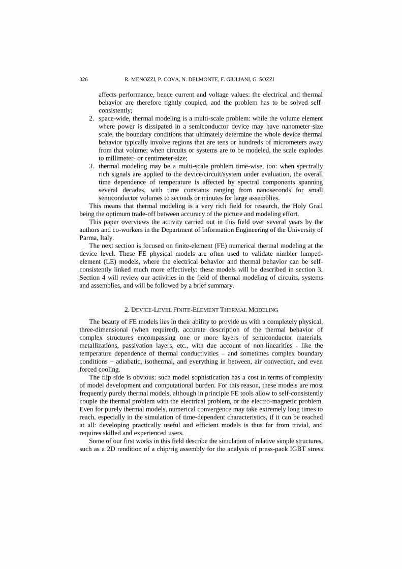
parameter extraction and model validation. Fig. 1 shows a schematic of the die and
package 3D structure (left) and the actual test rig we built for parameter extraction and
model tuning by comparison of measured and simulated temperatures (right).
Fig. 1 3D die and package structure for FE thermal modeling of power MOSFETs (left),
and the test rig (right) built for parameter extraction and model tuning [3].
In the same context, we also applied 3D FE thermal modeling to the study of passive
components, such as the inductors shown in Fig. 2 [4], [5].
The complexity and cost of 3D FE models obviously pay off most handsomely when
applied in the design phase, when investing in extensive accurate simulations makes good
economic sense if it allows to avoid taking unsatisfactory solutions all the way to the
prototyping phase. As an example, Fig. 3 shows a comparison among different
device/heat-sink assemblies [6].
While in the field of power converter applications, as illustrated in the examples
above, one is often interested in the determination of temperature profiles in assemblies
made of die, package, and often heat-sink, the device-level thermal simulation of
semiconductor devices for integrated circuits is typically focused on the semiconductor
alone – and possibly such top-side elements as metal lines and contacts, and passivation –
with the external world replaced by suitable boundary conditions: in this respect, the fact
that individual devices are often close-packed in regular patterns in integrated circuits
makes things a lot easier, since the planes separating adjacent devices can often be
replaced by adiabatic boundary conditions thanks to symmetry.
Cu, close to
the D.U.T.
Backside
FR4 surface
Top of the
package
Al drain flange
(through hole)

328 R. MENOZZI, P. COVA, N. DELMONTE, F. GIULIANI, G. SOZZI
Fig. 2 3D simulation of the temperature distribution in wound (left) [4] and planar (right) [5] transformers for switching power supplies; right scales in °C.
Fig. 3 3D FE simulations (bottom) of the temperature distribution in different device/heat-sink assemblies (top); right scales in °C [6].
From the point of view of the variety of materials and geometries, this is a comparatively simpler situation than the one we discussed before, where die/package/heat-sink assemblies are to be studied, and 2D analysis (as opposed to 3D) is often satisfactory; as such, it

Thermal and Electro-Thermal Modeling of Components and Systems... 329
allows the thermal problem and the electrical problem to be solved self-consistently, in
what may be called an Electro-Thermal (ET) simulation, where classical semiconductor
device equations (e.g., drift-diffusion equations plus electron and hole continuity
equations plus Poisson equation) are coupled with the heat transport equation. Here the
main problem is the dramatically different scale of the regions relevant for the electrical
and the thermal problem: while the former is typically in the nanometer to micrometer
range, the latter often measures hundreds of micrometers – think for instance about the
distance between the channel of a FET and the back-side wafer contact from which most
of the heat is dissipated. This is a significant computational challenge that can be
overcome with suitable techniques: an introductory review dealing with these problems
can be found in [7].
However, when the structure we want to simulate gets more complex and three-
dimensional, when features like top-side metal lines and contacts, passivation layer, etc.
cannot be neglected lest the thermal problem be significantly distorted, purely thermal
simulations – where the electrical problem is condensed in just one piece of information:
the location and size of the volume where power is dissipated – are again the weapon of
choice.
Our group in particular has worked extensively on the 3D thermal simulation of GaN-
based FETs. An example of device design guidelines provided by 3D FE simulations is
shown in Fig. 4 [8]. The importance of considering top-side heat spreading and heat
removal due to metal lines and contacts is shown in Fig. 5.
Fig. 4 Maximum power density that can be dissipated under a 150 K temperature increase
constraint in a 6-finger GaN HEMT as a function of finger width, finger spacing,
and substrate material (3D FE simulations) [8].

330 R. MENOZZI, P. COVA, N. DELMONTE, F. GIULIANI, G. SOZZI
Fig. 5 Simulated GaN HEMT structure (top) and channel temperature increase in a GaN
HEMT dissipating 3.5 W/mm (bottom); if the effect of top metal lines is neglected
(red dashed line) the self-heating is grossly overestimated. RTHL is the thermal
resistance of the top contacts. [8].
Obviously enough, top-side boundary conditions are not the only relevant ones. In the
case of GaN-based HEMTs, the thermal boundary resistance (TBR) between the GaN buffer
and the SiC/Si/sapphire substrate – due to phonon scattering at the hetero-interface - is
particularly significant; the die attach-layer is also a source of additional temperature
increase relative to the package back. Fig. 6 illustrates the importance of these two factors
[9]. In the dynamic simulations of Fig. 7 the TBR layer and the die attach are clearly visible.
Besides providing valuable guidelines in the design phase, FE thermal simulations are
extremely useful in the analysis of reliability results.
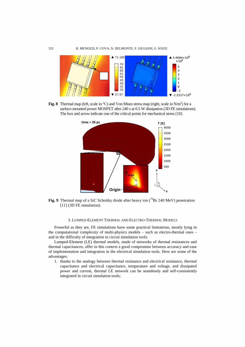
As an example, Fig. 8 [10] shows the FE-simulated thermal map and Von Mises stress
map of a surface-mounted power MOSFET undergoing thermal cycling. Here the thermal
simulation is part of a self-consistent thermo-mechanical model supporting the
interpretation of power cycle stress experiments.
In another recent reliability study, we also applied FE thermal simulation to the study
of the heavy ion irradiation damage in SiC Schottky diodes [11], [12], showing that the
ion penetration raises the junction temperature above the SiC melting point, as illustrated
by Fig. 9, with permanent device damage.

Thermal and Electro-Thermal Modeling of Components and Systems... 331
Fig. 6 Maximum temperature in a GaN HEMT as a function of the thermal conductance
of the TBR layer (blue curve, left) and of the die-attach layer (red curve, right) (3D
FE simulations) [9].
Fig. 7 Dynamic simulation of vertical temperature profiles following the application of a
power step in a GaN HEMT (3D FE simulations). The effect of the TBR layer and
of the die-attach can be seen in the temperature step at about 3 m depth and in the
steep temperature gradient at the back surface [9].
332 R. MENOZZI, P. COVA, N. DELMONTE, F. GIULIANI, G. SOZZI
Fig. 8 Thermal map (left, scale in °C) and Von Mises stress map (right, scale in N/m2) for a
surface-mounted power MOSFET after 240 s at 0.5 W dissipation (3D FE simulations).
The box and arrow indicate one of the critical points for mechanical stress [10].
Fig. 9 Thermal map of a SiC Schottky diode after heavy ion (79
Br 240 MeV) penetration
[11] (3D FE simulation).
3. LUMPED-ELEMENT THERMAL AND ELECTRO-THERMAL MODELS
Powerful as they are, FE simulations have some practical limitations, mostly lying in
the computational complexity of multi-physics models – such as electro-thermal ones –
and in the difficulty of integration in circuit simulation tools.
Lumped-Element (LE) thermal models, made of networks of thermal resistances and
thermal capacitances, offer in this context a good compromise between accuracy and ease
of implementation and integration in the electrical simulation tools. Here are some of the
advantages:
1. thanks to the analogy between thermal resistance and electrical resistance, thermal
capacitance and electrical capacitance, temperature and voltage, and dissipated
power and current, thermal LE network can be seamlessly and self-consistently
integrated in circuit simulation tools;
Thermal and Electro-Thermal Modeling of Components and Systems... 333
2. if desired, the model can retain a sound physical meaning, since thermal
resistances and capacitances can be calculated based on device geometry and
material properties; alternatively, more empirical models can be used, where
parameter values are optimized to get the best fit with measurements;
3. including conductive or convective boundary conditions, heat-spreading and heat-
sinking elements is relatively easy, and amounts to inserting additional thermal
resistances and capacitances between the device and the ambient.
3.1. Empirical LE thermal models: Foster and Cauer networks
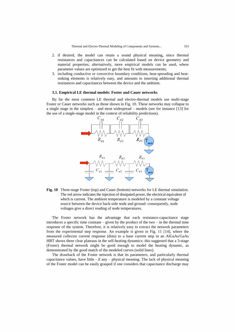
By far the most common LE thermal and electro-thermal models use multi-stage
Foster or Cauer networks such as those shown in Fig. 10. These networks may collapse to
a single stage in the simplest – and most widespread – models (see for instance [13] for
the use of a single-stage model in the context of reliability predictions).
Fig. 10 Three-stage Foster (top) and Cauer (bottom) networks for LE thermal simulation.
The red arrow indicates the injection of dissipated power, the electrical equivalent of
which is current. The ambient temperature is modeled by a constant voltage
source between the device back-side node and ground: consequently, node
voltages give a direct reading of node temperatures.
The Foster network has the advantage that each resistance-capacitance stage
introduces a specific time constant – given by the product of the two – in the thermal time
response of the system. Therefore, it is relatively easy to extract the network parameters
from the experimental step response. An example is given in Fig. 11 [14], where the
measured collector current response (dots) to a base current step in an AlGaAs/GaAs
HBT shows three clear plateaus in the self-heating dynamics: this suggested that a 3-stage
(Foster) thermal network might be good enough to model the heating dynamic, as
demonstrated by the good match of the modeled curves (solid lines).
The drawback of the Foster network is that its parameters, and particularly thermal
capacitance values, have little - if any – physical meaning. The lack of physical meaning
of the Foster model can be easily grasped if one considers that capacitance discharge may
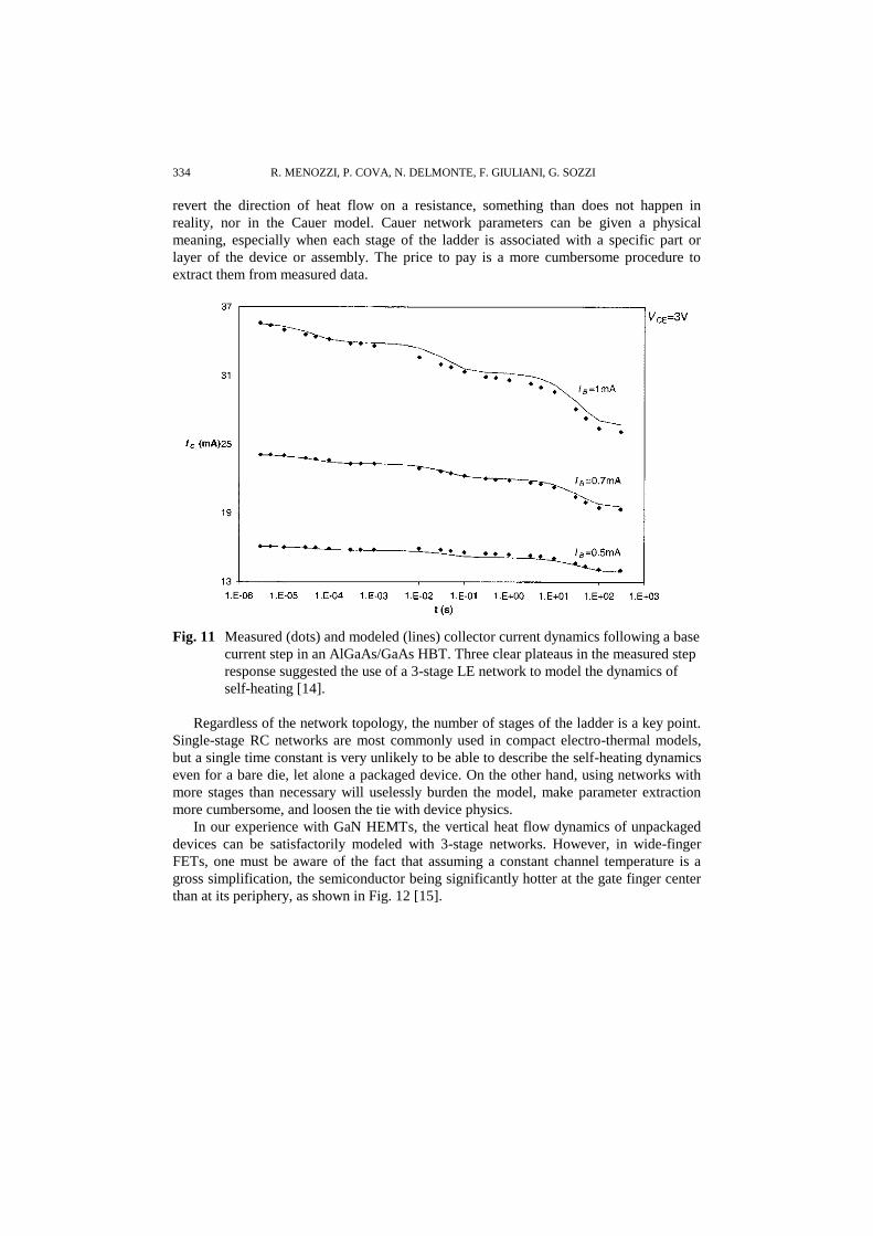
334 R. MENOZZI, P. COVA, N. DELMONTE, F. GIULIANI, G. SOZZI
revert the direction of heat flow on a resistance, something than does not happen in
reality, nor in the Cauer model. Cauer network parameters can be given a physical
meaning, especially when each stage of the ladder is associated with a specific part or
layer of the device or assembly. The price to pay is a more cumbersome procedure to
extract them from measured data.
Fig. 11 Measured (dots) and modeled (lines) collector current dynamics following a base
current step in an AlGaAs/GaAs HBT. Three clear plateaus in the measured step
response suggested the use of a 3-stage LE network to model the dynamics of
self-heating [14].
Regardless of the network topology, the number of stages of the ladder is a key point.
Single-stage RC networks are most commonly used in compact electro-thermal models,
but a single time constant is very unlikely to be able to describe the self-heating dynamics
even for a bare die, let alone a packaged device. On the other hand, using networks with
more stages than necessary will uselessly burden the model, make parameter extraction
more cumbersome, and loosen the tie with device physics.
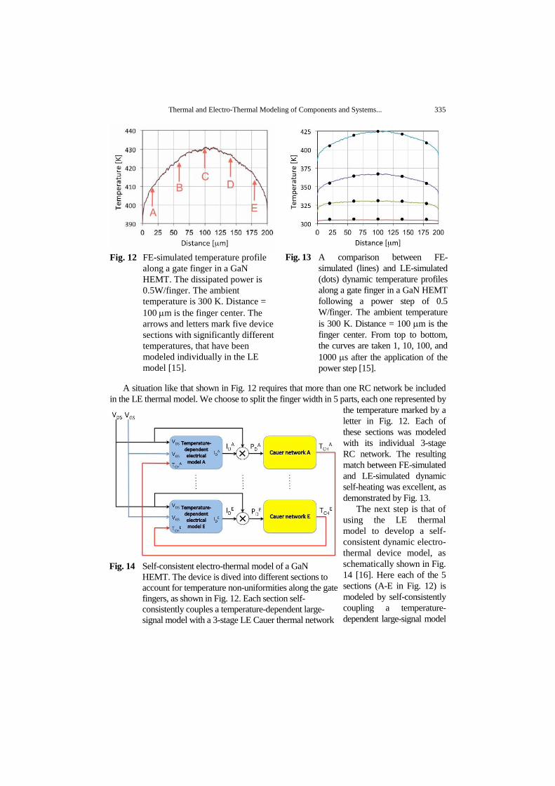
In our experience with GaN HEMTs, the vertical heat flow dynamics of unpackaged
devices can be satisfactorily modeled with 3-stage networks. However, in wide-finger
FETs, one must be aware of the fact that assuming a constant channel temperature is a
gross simplification, the semiconductor being significantly hotter at the gate finger center
than at its periphery, as shown in Fig. 12 [15].
Thermal and Electro-Thermal Modeling of Components and Systems... 335
A situation like that shown in Fig. 12 requires that more than one RC network be included in the LE thermal model. We choose to split the finger width in 5 parts, each one represented by
the temperature marked by a letter in Fig. 12. Each of these sections was modeled with its individual 3-stage RC network. The resulting match between FE-simulated and LE-simulated dynamic self-heating was excellent, as demonstrated by Fig. 13.
The next step is that of using the LE thermal model to develop a self-consistent dynamic electro-thermal device model, as schematically shown in Fig. 14 [16]. Here each of the 5 sections (A-E in Fig. 12) is modeled by self-consistently coupling a temperature-dependent large-signal model
Fig. 12 FE-simulated temperature profile along a gate finger in a GaN HEMT. The dissipated power is 0.5W/finger. The ambient temperature is 300 K. Distance = 100 m is the finger center. The arrows and letters mark five device sections with significantly different temperatures, that have been modeled individually in the LE model [15].
Fig. 13 A comparison between FE-simulated (lines) and LE-simulated (dots) dynamic temperature profiles along a gate finger in a GaN HEMT following a power step of 0.5 W/finger. The ambient temperature is 300 K. Distance = 100 m is the finger center. From top to bottom, the curves are taken 1, 10, 100, and 1000 s after the application of the power step [15].
Fig. 14 Self-consistent electro-thermal model of a GaN HEMT. The device is dived into different sections to account for temperature non-uniformities along the gate fingers, as shown in Fig. 12. Each section self-consistently couples a temperature-dependent large-signal model with a 3-stage LE Cauer thermal network [16].

336 R. MENOZZI, P. COVA, N. DELMONTE, F. GIULIANI, G. SOZZI
with a 3-stage LE Cauer thermal network, for a complete dynamic description of self-heating
including temperature non-uniformities along the gate fingers and amenable to easy integration
in circuit simulation tools.
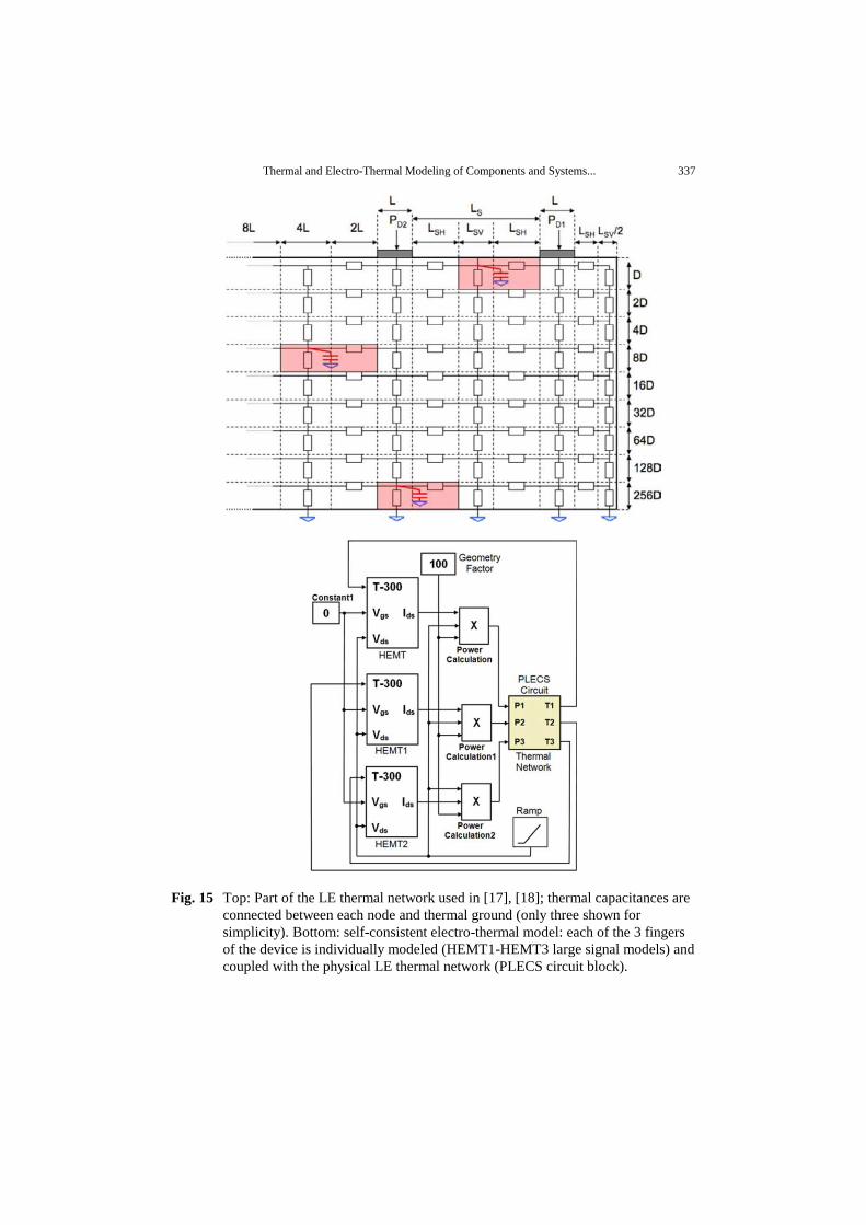
3.2. Physical LE thermal networks
We developed another successful approach to LE thermal and electro-thermal
modeling, whereby the thermal RC network is a physical representation of the 2D or 3D
structure of the device under study.
This concept was first applied to the 2D cross-section of unpackaged GaN-HEMTs
[17], [18]. Here a physical LE thermal network was self-consistently coupled with a
temperature-dependent large-signal FET model as shown in Fig. 15 for dynamic
description of self heating, including the 2D temperature distribution over the whole
structure. A 3D extension of this approach is exemplified in [9] and [19]. The modeled
results were compared with FE simulations and with experimental data with good success.
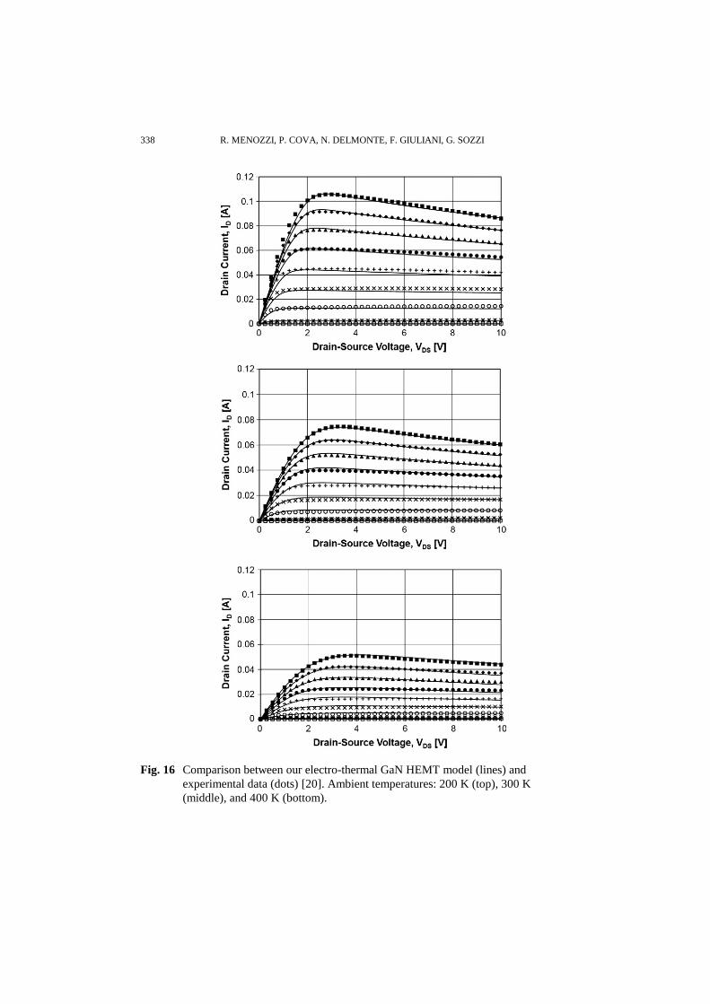
The model was later enhanced including the effect of trapping phenomena [20], a
significant concern for GaN FETs. Fig. 16 shows the excellent match between measured
and modeled DC output characteristics at different temperatures, while Fig. 17 is an
illustration of the interplay between thermal and trapping dynamic in the pulsed response
of these – and other – devices.
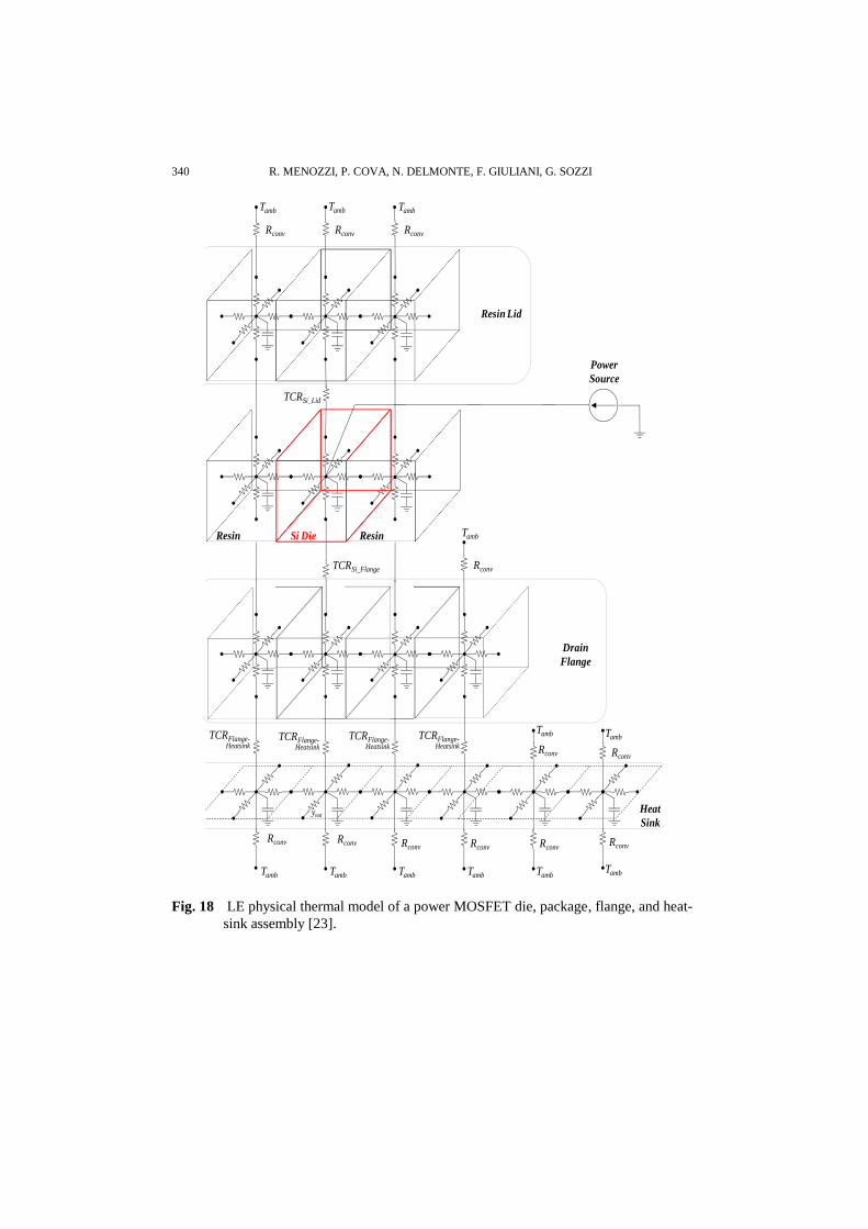
This physical LE modeling approach has been applied with good results to power
MOSFET assemblies (see Fig. 18) [21]-[23], as well as to nanometer-scale SOI FinFETs [24].
4. CIRCUIT- AND SYSTEM-LEVEL FE THERMAL MODELS
FE thermal simulations, so far considered at device or device-plus-package level, can
be effectively used at higher hierarchical levels, to describe the thermal behavior of
circuits and boards including several active and passive devices, metal lines, heat-sinks,
etc. The building blocks are in this case the FE models of the individual components, such
as those described in section 2. However, for practical reasons the whole circuit/system
FE model can hardly be built by assembling detailed device-level models like those of
Figs. 1-3 and 8, due to the excessive number of degrees of freedom of the FE simulation,
and the attendant overhead and convergence problems. Once detailed FE models of the
individual components are available, the first step of the circuit/system modeling process
is a simplification of the device models aimed at obtaining nimbler models amenable to
integration in the whole circuit/system without simulation overburden, but at the same
time retaining the fundamental and necessary amount of information on their thermal
behavior. An example of this simplification process is shown in Fig. 19 [25].
In particular, we applied this technique to the thermal simulation of converter modules
for DC power supplies in the context of the re-design of the electronics for one of the
experiments of the CERN’s ATLAS project [4], [25]-[28]. An example of circuit-level FE
thermal simulation, and its experimental validation, is given by Fig. 20.
In this context, accurate description of thermal boundary conditions is key: this is
often no trivial task, sometimes requiring thermal and fluid-dynamics simulation of water
heat-sinks [29]-[31], as shown in Fig. 21.
Thermal and Electro-Thermal Modeling of Components and Systems... 337
Fig. 15 Top: Part of the LE thermal network used in [17], [18]; thermal capacitances are
connected between each node and thermal ground (only three shown for
simplicity). Bottom: self-consistent electro-thermal model: each of the 3 fingers
of the device is individually modeled (HEMT1-HEMT3 large signal models) and
coupled with the physical LE thermal network (PLECS circuit block).
338 R. MENOZZI, P. COVA, N. DELMONTE, F. GIULIANI, G. SOZZI
Fig. 16 Comparison between our electro-thermal GaN HEMT model (lines) and
experimental data (dots) [20]. Ambient temperatures: 200 K (top), 300 K
(middle), and 400 K (bottom).

Thermal and Electro-Thermal Modeling of Components and Systems... 339
Fig. 17 Modeled gate-lag response of a GaN HEMT, in the case of a bulk donor trap
(top) and a surface donor trap (bottom) [20]. The ambient temperature is 300 K.
340 R. MENOZZI, P. COVA, N. DELMONTE, F. GIULIANI, G. SOZZI
yout
Rconv
Tamb
Rconv
Tamb
HeatSink
DrainFlange
PowerSource
Rconv
Tamb
Rconv
Tamb
Rconv
Tamb
Rconv
Tamb
Rconv
Tamb
Rconv
Tamb
Rconv
Tamb
Rconv
Tamb
Rconv
Tamb
Rconv
Tamb
Resin Lid
Si Die ResinResin
TCRSi_Lid
TCRSi_Flange
TCRFlange-Heatsink
TCRFlange-Heatsink
TCRFlange-Heatsink
TCRFlange-Heatsink
Fig. 18 LE physical thermal model of a power MOSFET die, package, flange, and heat-sink assembly [23].

Thermal and Electro-Thermal Modeling of Components and Systems... 341
Fig. 19 An example of detailed FE thermal model for rectifier diodes in ISOTOP package (left) and it simplified version (right) for circuit simulation [25].
Fig. 20 An example of FE thermal model (top) and experimental IR thermal map (bottom) for a single-module DC/DC converter [25]. The output power is 1.2 kW, and forced-air cooling is in place. The maximum temperature error is 8% all over the board.

342 R. MENOZZI, P. COVA, N. DELMONTE, F. GIULIANI, G. SOZZI
Fig. 21 FE simulation of a converter board on a water-cooled heat-sink [30]. Top: water
velocity in the hear sink; bottom: thermal simulation of the converter and heat-sink.
5. SUMMARY
In this paper we have reviewed the activity carried out over several years at the
Department of Information Engineering of the University of Parma, Italy, in the field of
thermal and electro-thermal modeling of devices, device and package assemblies, circuits,
and systems encompassing active boards and heat-sinking elements.
We have shown examples of the use of Finite-Element (FE) 3D tools for the thermal
analysis of a hierarchy of structures ranging from bare device dies to complex systems
including active and passive devices, boards, metallizations, and air- and water-cooled
heat-sinks. Increasing the level of complexity requires developing smart solutions for the
reduction of model complexity, lest numerical convergence be slowed down beyond
acceptable limits, or made altogether impossible.
A variety of Lumped-Element modeling examples has also been shown. These models
lose some of the physical detail of FE models, but are amenable to integration inside
circuit simulation tools, thus allowing self-consistent electro-thermal simulation of the
device or circuit under realistic operating conditions, something that is practically
impossible with FE tools. These models can range from purely empirical to strictly
physics- and geometry-based.
Thermal and Electro-Thermal Modeling of Components and Systems... 343
REFERENCES
[1] P. Cova, G. Nicoletto, A. Pirondi, M. Portesine, M. Pasqualetti, "Power cycling on press-pack IGBTs:
measurements and thermomechanical simulation", Microel. Reliab., vol. 39, pp. 1165–1170, 1999.
[2] P. Cova, F. Fasce, P. Pampili, M. Portesine, G. Sozzi, P. E. Zani, "High reliable high power diode for
welding applications", Microel. Reliab., vol. 44, pp. 1437–1441, 2004.
[3] P. Cova, N. Delmonte, R. Menozzi, "Thermal characterization and modeling of power hybrid converters
for distributed power systems", Microel. Reliab., vol. 46, pp. 1760–1765, 2006.
[4] P. Cova, N. Delmonte, R. Menozzi, "Thermal modeling of high-frequency DC/DC switching modules:
electromagnetic and thermal simulation of magnetic components", Microel. Reliab., vol. 48, pp. 1468–
1472, 2008.
[5] M. Bernardoni, N. Delmonte, P. Cova, R. Menozzi, "Thermal modeling of planar transformer for
switching power converters", Microel. Reliab., vol. 50, pp. 1778–1782, 2010.
[6] M. Bernardoni, P. Cova, N. Delmonte, R. Menozzi, "Heat management for power converters in sealed
enclosures: A numerical study", Microel. Reliab., vol. 49, pp. 1293–1298, 2009.
[7] G. Sozzi, R. Menozzi, "A review of the use of electro-thermal simulations for the analysis of
heterostructure FETs", Microel. Reliab., vol. 47, pp. 65–73, 2007.
[8] F. Bertoluzza, N. Delmonte, R. Menozzi, "Three-dimensional finite-element thermal simulation of GaN-
based HEMTs", Microel. Reliab., vol. 49, pp. 468–473, 2009.
[9] M. Bernardoni, N. Delmonte, R. Menozzi, "Modeling of the impact of boundary conditions on
AlGaN/GaN HEMT self heating", In Proc. 2011 Int. Conf. Compound Semiconductor Manufacturing
Technology (CS-MANTECH), pp. 229-232, 2011.
[10] N. Delmonte, F. Giuliani, P. Cova, "Finite element modeling and characterization of lead-free solder
joints fatigue life during power cycling of surface mounting power devices", Microel. Reliab., vol. 53,
pp. 1611–1616, 2013.
[11] C. Abbate, G. Busatto, P. Cova, N. Delmonte, F. Giuliani, F. Iannuzzo, A. Sanseverino, F. Velardi,
"Thermal damage in SiC Schottky diods induced by SE heavy ions", Microel. Reliab., vol. 54,
pp. 2200–2206, 2014.
[12] C. Abbate, G. Busatto, P. Cova, N. Delmonte, F. Giuliani, F. Iannuzzo, A. Sanseverino, F. Velardi,
"Analysis of heavy ion irradiation induced thermal damage", IEEE Trans. Nucl. Sci., vol. 62, pp. 202-
219, 2015.
[13] M. Ciappa, F. Carbognani, P. Cova, W. Fichtner, "A novel thermomechanics-based lifetime prediction
model for cycle fatigue failure mechanisms in in power semiconductors", Microel. Reliab., vol. 42,
pp. 1653–1658, 2002.
[14] M. Busani, R. Menozzi, M. Borgarino, F. Fantini, "Dynamic thermal characterization and modeling of
packaged AlGaAs/GaAs HBTs", IEEE Trans. Components Packaging Technologies, vol. 23, pp. 352-
359, 2000.
[15] M. Bernardoni, N. Delmonte, R. Menozzi, "Empirical and physical modeling of self-heating in power
AlGaN/GaN HEMT", In Proc. 2012 Int. Conf. Compound Semiconductor Manufacturing Technology
(CS-MANTECH), pp. 95-98, 2012.
[16] F. Giuliani, N. Delmonte, P. Cova, R. Menozzi, "GaN HEMTs for power switching applications: from
device to system-level electro-thermal modeling", In Proc. 2013 Int. Conf. Compound Semiconductor
Manufacturing Technology (CS-MANTECH), pp. 215-218, 2013.
[17] F. Bertoluzza, G. Sozzi, N. Delmonte, R. Menozzi, "Lumped element thermal modeling of GaN-based
HEMT", In Proc. 2009 IEEE MTT-S Int. Microwave Symp. Dig., pp. 973-976, 2009.
[18] F. Bertoluzza, G. Sozzi, N. Delmonte, R. Menozzi, "Hybrid large-signal/lumped-element electro-thermal
modeling of GaN-HEMTs", IEEE Trans. Microw. Th. Techn., vol. 57, pp. 3163-3170, 2009.
[19] M. Bernardoni, N. Delmonte, G. Sozzi, R. Menozzi, "Large-signal GaN HEMT electro-thermal model
with 3D dynamic description of self-heating", In Proc. 41th European Solid-State Device Research Conf.
(ESSDERC), pp. 171-174, 2011.
[20] D. Mari, M. Bernardoni, G. Sozzi, R. Menozzi, G. A. Umana-Membreno, B. D. Nener, "A physical
large-signal model for GaN HEMTs including self-heating and trap-related dispersion", Microel. Reliab.,
vol. 51, pp. 229–234, 2011.
[21] P. Cova, M. Bernardoni, "A MATLAB based approach for electro-thermal design of power converters",
In Proc. 6th Int. Conf. Integrated Power Electronics Systems (CIPS), pp. 407-411, 2010.

344 R. MENOZZI, P. COVA, N. DELMONTE, F. GIULIANI, G. SOZZI
[22] M. Bernardoni, N. Delmonte, P. Cova, R. Menozzi, "Self-consistent compact electrical and thermal
modeling of power devices including package and heat-sink", In Proc. IEEE Int. Symp. Power
Electronics Systems, Electrical Drives, Automation and Motion (SPEEDAM), pp. 556-561, 2010.
[23] P. Cova, M. Bernardoni, N. Delmonte, R. Menozzi, "Dynamic electro-thermal modeling for power
device assemblies" Microel. Reliab., vol. 51, pp. 1948–1953, 2011.
[24] M. Bernardoni, N. Delmonte, R. Menozzi, "Lumped-element thermal modeling of SOI FinFETs", In
Proc. APMC10/ICONN2012/ACMM22, paper 1096, 2012.
[25] M. Alderighi, M. Citterio, M. Riva, S. Latorre, A. Costabeber, A. Paccagnella, F. Sichirollo, G. Spiazzi,
M. Stellini, P. Tenti, P. Cova, N. Delmonte, A. Lanza, M. Bernardoni, R. Menozzi, S. Baccaro, F.
Iannuzzo, A. Sanseverino, G. Busatto, V. De Luca, F. Velardi, "Power converters for future LHC
experiments", J. Instrumentation (JINST), vol. 7, C03012, 2012.
[26] P. Tenti, G. Spiazzi, S. Buso, M. Riva, P. Maranesi, F. Belloni, P. Cova, R. Menozzi, N. Delmonte, M.
Bernardoni, F. Iannuzzo, G. Busatto, A. Porzio, F. Velardi, A. Lanza, M. Citterio, C. Meroni, "Power
supply distribution system for calorimeters at the LHC beyond the nominal luminosity", J.
Instrumentation (JINST), vol. 6, P06005, 2011.
[27] S. Baccaro, G. Busatto, M. Citterio, P. Cova, N. Delmonte, F. Iannuzzo, A. Lanza, M. Riva, A.
Sanseverino, G. Spiazzi, "Reliability oriented deign of power supplies for high energy physics
applications", Microel. Reliab., vol. 52, pp. 2465–2470, 2012.
[28] P. Cova and N. Delmonte, "Thermal modeling and design of power converters with tight thermal
constraints", Microel. Reliab., vol. 52, pp. 2391–2396, 2012.
[29] P. Cova, N. Delmonte, P. Pampili, M. Portesine, P. E. Zani, "Finite element design of water heat sinks
for press-pack IGBTs", In Proc. 4th Int. Conf. Integrated Power Electronics Systems (CIPS), pp. 353-357,
2006.
[30] P. Cova, N. Delmonte, F. Giuliani, M. Citterio, S. Latorre, M. Lazzaroni, A. Lanza, "Thermal
optimization of water heat sink for power converters with tight thermal constraints", Microel. Reliab.,
vol. 53, pp. 1760–1765, 2013.
[31] M. Lazzaroni, M. Citterio, S. Latorre, A. Lanza, P. Cova, N. Delmonte, F. Giuliani, "Thermal modeling
and characterization for designing reliable power converters for LHC power supplies", Acta IMEKO J.,
vol. 14, pp. 17-25, 2014.