theoretical investigation on the structural stability of gap nanowires with facets
TRANSCRIPT
Applied Surface Science 256 (2009) 1054–1057
Theoretical investigation on the structural stability of GaP nanowireswith f1 1 1g facets
Tomoki Yamashita *, Toru Akiyama, Kohji Nakamura, Tomonori Ito
Department of Physics Engineering, Mie University, 1577 Kurima-Machiya, Tsu, Mie 514-8507, Japan
A R T I C L E I N F O
Article history:
Available online 23 June 2009
PACS:
81.07.Bc
81.10.�h
61.46.+w
Keywords:
Nanowires
GaP
Structural stability
f1 1 1g Facets
f1 1 0g Facets
A B S T R A C T
The structural stability of GaP nanowires (NWs) with f1 1 1g facets including twin planes is
systematically investigated using our empirical potentials which incorporate the electrostatic
interaction between surface cations and anions. The cohesive energy of GaP NWs for diameter of
�30 nm demonstrates that the wurtzite structure is the most stable over entire diameter range. This is
because the electrostatic interaction between surface cations and anions is dominant around twin
planes, resulting in the small energy deficit compared to that on polar f1 1 1g facets. By comparing the
cohesive energy of GaP NWs consisting of f1 1 1g=f1 1 0 0g facets with that of f1 1 0g=f1 1 2 0g facets, the
NWs consisting of f1 1 0g=f1 1 2 0g facets are found to be favorable than those consisting of
f1 1 1g=f1 1 0 0g facets over entire diameter range. These results imply that growth processes such
as vapor–liquid–solid mechanism could affect on the formation of NWs consisting of f1 1 1g=f1 1 0 0gfacets.
� 2009 Elsevier B.V. All rights reserved.
Contents lists available at ScienceDirect
Applied Surface Science
journal homepage: www.e lsev ier .com/ locate /apsusc
1. Introduction
Semiconductor nanowires (NWs) have attracted much atten-tion recently owing to their fundamental importance in reduceddimensionality and size in optical, electrical, and mechanicalproperties and their wide range of potential application innanoscale devices. In particular, III–V NWs seem to be highlypromising because of their specific optical properties and areexpected to be applied to light-emitting diodes [1–3], photo-detectors [4,5] and lasers [6–8]. Hence, considerable efforts havebeen devoted to fabricate these NWs by employing variousmethods such as metal-organic vapor-phase epitaxy [9,10] andmolecular-beam epitaxy [11–13], and many theoretical studieshave been carried out [14–17]. Actually, these studies have foundthat there are some structural characteristics different from bulkcrystals: III–V NWs grown in the [1 1 1] direction often include thewurtzite (W) segments in the zinc blende (ZB) structure [18–24].
It has been recently reported that GaP NWs along the [1 1 1]direction fabricated by the vapor–liquid–solid (VLS) mechanismare terminated by f1 1 1g (f1 1 0 0g in the W structure) facets[18,19], while GaAs NWs [20,21], InP NWs [22], and InAs NWs [23]grown by the selective area (SA) growth form a hexagonal cylinderwith f1 1 0g (f1 1 2 0g in the W structure) facets. Since GaP NWs
* Corresponding author. Tel.: +81 59 232 1211x3978; fax: +81 59 231 9726.
E-mail address: [email protected] (T. Yamashita).
0169-4332/$ – see front matter � 2009 Elsevier B.V. All rights reserved.
doi:10.1016/j.apsusc.2009.04.204
with f1 1 1g=f1 1 0 0g facets reported by Johansson et al. [18,19]consist of octahedral segments whose boundaries are twin planes,the cross-section turns from hexagonal shape (triangular shape) totriangular shape (hexagonal shape) as the NW grows in the ZBstacking sequence. Indeed, the high resolution transmissionelectron microscopy (HRTEM) observation has shown such kindof microfaceted surface, indicating that GaP NWs withf1 1 1g=f1 1 0 0g facets tend to have the W structure for diameterranging from 50 to 100 nm.
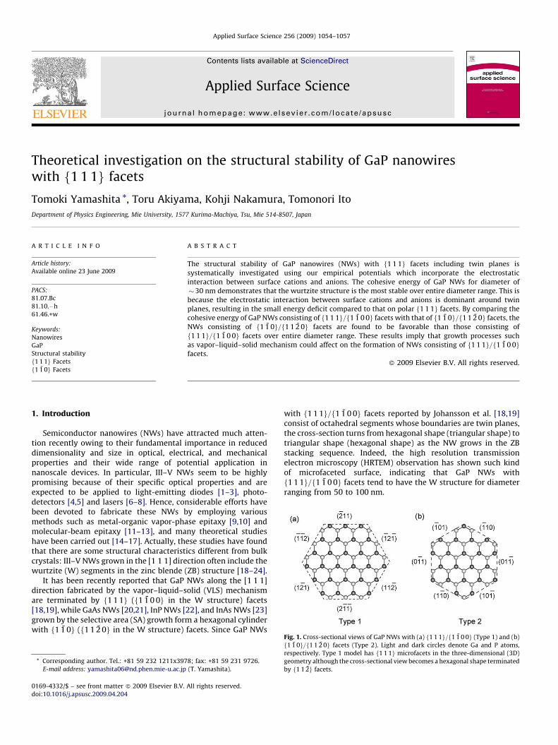
Fig. 1. Cross-sectional views of GaP NWs with (a) f1 1 1g=f1 1 0 0g (Type 1) and (b)
f1 1 0g=f1 1 2 0g facets (Type 2). Light and dark circles denote Ga and P atoms,
respectively. Type 1 model has f1 1 1g microfacets in the three-dimensional (3D)
geometry although the cross-sectional view becomes a hexagonal shape terminated
by f1 1 2g facets.
T. Yamashita et al. / Applied Surface Science 256 (2009) 1054–1057 1055
In spite of these findings, there are very few studies for therelationship between the orientation of NW facets and thestructural stability from theoretical viewpoints. In our previousstudy, for III–V NWs, the relative stability between the W and ZBstructures consisting of f1 1 0 0g and f1 1 0g facets, respectively,has been successfully investigated based on an empiricalinteratomic potential calculations [14]. In this study, thestructural stability of GaP NWs with f1 1 1g=f1 1 0 0g andf1 1 0g=f1 1 2 0g facets is systematically investigated based onour empirical interatomic potential calculations which can treatsmall energy difference caused by twin planes. Furthermore, wediscuss the relationship between the structural stability and the
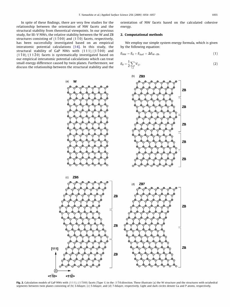
Fig. 2. Calculation models of GaP NWs with f1 1 1g=f1 1 0 0g facets (Type 1) in the h1 1 0
segments between twin planes consisting of (b) 3-bilayer, (c) 5-bilayer, and (d) 7-bilay
orientation of NW facets based on the calculated cohesiveenergy.
2. Computational methods
We employ our simple system energy formula, which is givenby the following equation:
ENW ¼ E0 þ ESurf þDEW�ZB; (1)
E0 ¼1
2
X
i; j
Vi j; (2)
idirection. These illustrate (a) the W structure and the structures with octahedral
er, respectively. Light and dark circles denote Ga and P atoms, respectively.
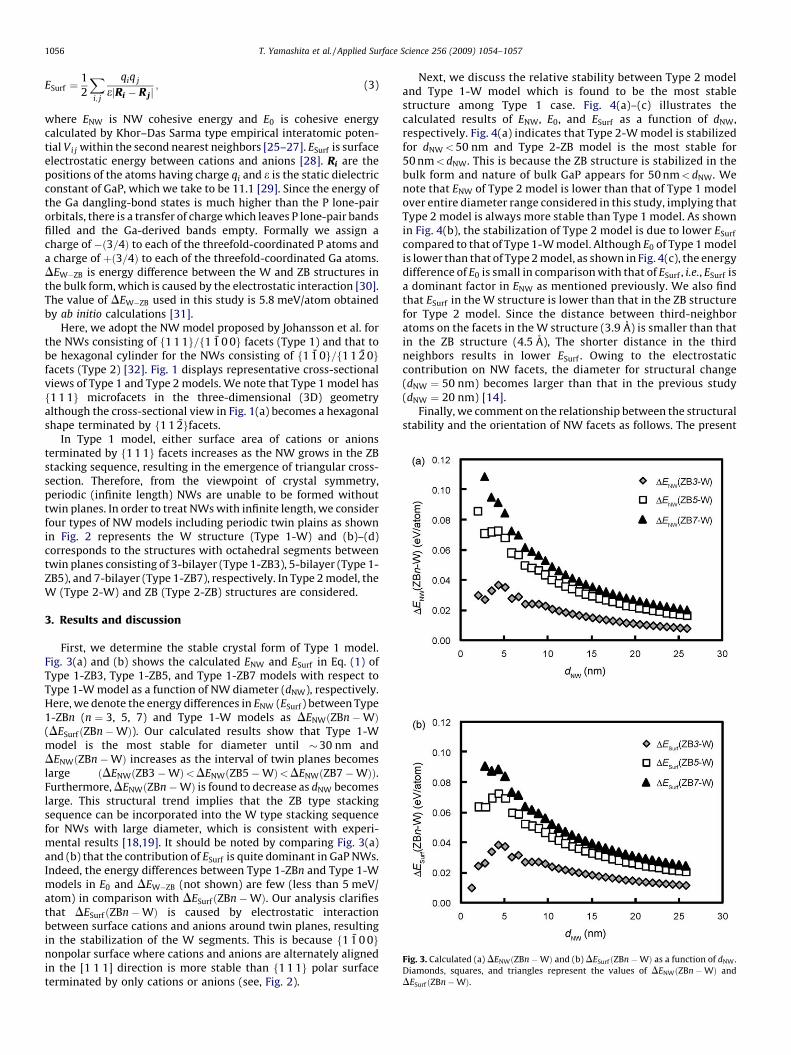
Fig. 3. Calculated (a) DENWðZBn�WÞ and (b) DESurf ðZBn�WÞ as a function of dNW.
Diamonds, squares, and triangles represent the values of DENWðZBn�WÞ and
DESurf ðZBn�WÞ.
e Science 256 (2009) 1054–1057
ESurf ¼1
2
X
i; j
qiq j
ejRi � R jj; (3)
where ENW is NW cohesive energy and E0 is cohesive energycalculated by Khor–Das Sarma type empirical interatomic poten-tial Vi j within the second nearest neighbors [25–27]. ESurf is surfaceelectrostatic energy between cations and anions [28]. Ri are thepositions of the atoms having charge qi and e is the static dielectricconstant of GaP, which we take to be 11.1 [29]. Since the energy ofthe Ga dangling-bond states is much higher than the P lone-pairorbitals, there is a transfer of charge which leaves P lone-pair bandsfilled and the Ga-derived bands empty. Formally we assign acharge of �ð3=4Þ to each of the threefold-coordinated P atoms anda charge of þð3=4Þ to each of the threefold-coordinated Ga atoms.DEW�ZB is energy difference between the W and ZB structures inthe bulk form, which is caused by the electrostatic interaction [30].The value of DEW�ZB used in this study is 5.8 meV/atom obtainedby ab initio calculations [31].
Here, we adopt the NW model proposed by Johansson et al. forthe NWs consisting of f1 1 1g=f1 1 0 0g facets (Type 1) and that tobe hexagonal cylinder for the NWs consisting of f1 1 0g=f1 1 2 0gfacets (Type 2) [32]. Fig. 1 displays representative cross-sectionalviews of Type 1 and Type 2 models. We note that Type 1 model hasf1 1 1g microfacets in the three-dimensional (3D) geometryalthough the cross-sectional view in Fig. 1(a) becomes a hexagonalshape terminated by f1 1 2gfacets.
In Type 1 model, either surface area of cations or anionsterminated by f1 1 1g facets increases as the NW grows in the ZBstacking sequence, resulting in the emergence of triangular cross-section. Therefore, from the viewpoint of crystal symmetry,periodic (infinite length) NWs are unable to be formed withouttwin planes. In order to treat NWs with infinite length, we considerfour types of NW models including periodic twin plains as shownin Fig. 2 represents the W structure (Type 1-W) and (b)–(d)corresponds to the structures with octahedral segments betweentwin planes consisting of 3-bilayer (Type 1-ZB3), 5-bilayer (Type 1-ZB5), and 7-bilayer (Type 1-ZB7), respectively. In Type 2 model, theW (Type 2-W) and ZB (Type 2-ZB) structures are considered.
3. Results and discussion
First, we determine the stable crystal form of Type 1 model.Fig. 3(a) and (b) shows the calculated ENW and ESurf in Eq. (1) ofType 1-ZB3, Type 1-ZB5, and Type 1-ZB7 models with respect toType 1-W model as a function of NW diameter (dNW), respectively.Here, we denote the energy differences in ENW (ESurf ) between Type1-ZBn (n ¼ 3, 5, 7) and Type 1-W models as DENWðZBn�WÞ(DESurf ðZBn�WÞ). Our calculated results show that Type 1-Wmodel is the most stable for diameter until �30 nm andDENWðZBn�WÞ increases as the interval of twin planes becomeslarge ðDENWðZB3�WÞ<DENWðZB5�WÞ<DENWðZB7�WÞÞ.Furthermore, DENWðZBn�WÞ is found to decrease as dNW becomeslarge. This structural trend implies that the ZB type stackingsequence can be incorporated into the W type stacking sequencefor NWs with large diameter, which is consistent with experi-mental results [18,19]. It should be noted by comparing Fig. 3(a)and (b) that the contribution of ESurf is quite dominant in GaP NWs.Indeed, the energy differences between Type 1-ZBn and Type 1-Wmodels in E0 and DEW�ZB (not shown) are few (less than 5 meV/atom) in comparison with DESurfðZBn�WÞ. Our analysis clarifiesthat DESurf ðZBn�WÞ is caused by electrostatic interactionbetween surface cations and anions around twin planes, resultingin the stabilization of the W segments. This is because f1 1 0 0gnonpolar surface where cations and anions are alternately alignedin the [1 1 1] direction is more stable than f1 1 1g polar surfaceterminated by only cations or anions (see, Fig. 2).
T. Yamashita et al. / Applied Surfac1056
Next, we discuss the relative stability between Type 2 modeland Type 1-W model which is found to be the most stablestructure among Type 1 case. Fig. 4(a)–(c) illustrates thecalculated results of ENW, E0, and ESurf as a function of dNW,respectively. Fig. 4(a) indicates that Type 2-W model is stabilizedfor dNW <50 nm and Type 2-ZB model is the most stable for50 nm< dNW. This is because the ZB structure is stabilized in thebulk form and nature of bulk GaP appears for 50 nm< dNW. Wenote that ENW of Type 2 model is lower than that of Type 1 modelover entire diameter range considered in this study, implying thatType 2 model is always more stable than Type 1 model. As shownin Fig. 4(b), the stabilization of Type 2 model is due to lower ESurf
compared to that of Type 1-W model. Although E0 of Type 1 modelis lower than that of Type 2 model, as shown in Fig. 4(c), the energydifference of E0 is small in comparison with that of ESurf , i.e., ESurf isa dominant factor in ENW as mentioned previously. We also findthat ESurf in the W structure is lower than that in the ZB structurefor Type 2 model. Since the distance between third-neighboratoms on the facets in the W structure (3.9 A) is smaller than thatin the ZB structure (4.5 A), The shorter distance in the thirdneighbors results in lower ESurf . Owing to the electrostaticcontribution on NW facets, the diameter for structural change(dNW ¼ 50 nm) becomes larger than that in the previous study(dNW ¼ 20 nm) [14].
Finally, we comment on the relationship between the structuralstability and the orientation of NW facets as follows. The present
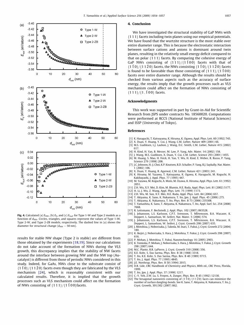
Fig. 4. Calculated (a) ENW, (b) E0, and (c) ESurf for Type 1-W and Type 2 models as a
function of dNW. Circles, triangles, and squares represent the values of Type 1-W,
Type 2-W, and Type 2-ZB models, respectively. The dashed line in (a) shows the
diameter for structural change (dNW ¼ 50 nm).
T. Yamashita et al. / Applied Surface Science 256 (2009) 1054–1057 1057
results for stable NW shape (Type 2 is stable) are different fromthose obtained by the experiments [18,19]. Since our calculationsdo not take account of the formation of NWs during the VLSgrowth, this discrepancy implies that the stability of NW facetsaround the interface between growing NW and the NW top (Au-catalyst) is different from those of periodic NWs considered in thisstudy. Indeed, for GaAs, NWs close to the substrate consist off1 1 0g=f1 1 2 0g facets even though they are fabricated by the VLSmechanism [24], which is reasonably consistent with ourcalculated results. Therefore, it is implied that the growthprocesses such as VLS mechanism could affect on the formationof NWs consisting of f1 1 1g=f1 1 0 0gfacets.
4. Conclusion
We have investigated the structural stability of GaP NWs withf1 1 1g facets including twin planes using our empirical potentials.We have found that the wurtzite structure is the most stable overentire diameter range. This is because the electrostatic interactionbetween surface cations and anions is dominant around twinplanes, resulting in the relatively small energy deficit compared tothat on polar f1 1 1g facets. By comparing the cohesive energy ofGaP NWs consisting of f1 1 1g=f1 1 0 0g facets with that off1 1 0g=f1 1 2 0g facets, the NWs consisting f1 1 0g=f1 1 2 0g facetsis found to be favorable than those consisting of f1 1 1g=f1 1 0 0gfacets over entire diameter range. Although the results should bechecked from various aspects such as the accuracy of surfaceenergy, the results imply that the growth processes such as VLSmechanism could affect on the formation of NWs consisting off1 1 1g=f1 ; 1 0 0g facets.
Acknowledgments
This work was supported in part by Grant-in-Aid for ScientificResearch from JSPS under contracts No. 18560020. Computationswere performed at RCCS (National Institute of Natural Sciences)and ISSP (University of Tokyo).
References
[1] K. Haraguchi, T. Katsuyama, K. Hiruma, K. Ogawa, Appl. Phys. Lett. 60 (1992) 745.[2] X. Duan, Y. Huang, Y. Cui, J. Wang, C.M. Lieber, Nature 409 (2001) 66.[3] M.S. Gudiksen, L.J. Lauhon, J. Wang, D.C. Smith, C.M. Lieber, Nature 415 (2002)
617.[4] H. Kind, H. Yan, B. Messer, M. Law, P. Yang, Adv. Mater. 14 (2002) 158.[5] J. Wang, M.S. Gudiksen, X. Duan, Y. Cui, C.M. Lieber, Science 293 (2001) 1455.[6] M. Huang, S. Mao, H. Feick, H. Yan, Y. Wu, H. Kind, E. Weber, R. Russo, P. Yang,
Science 279 (1998) 208.[7] J.C. Johnson, H.-J. Choi, K.P. Knutsen, R.D. Schaller, P. Yang, R.J. Saykally, Nat. Mater.
1 (2002) 106.[8] X. Duan, Y. Huang, R. Agarwal, C.M. Lieber, Nature 421 (2003) 241.[9] K. Hiruma, M. Yazawa, T. Katsuyama, K. Ogawa, K. Haraguchi, M. Koguchi, H.
Kakibayashi, J. Appl. Phys. 77 (1995) 447.[10] M. Yazawa, M. Koguchi, A. Muto, M. Ozawa, K. Hiruma, Appl. Phys. Lett. 61 (1992)
2051.[11] Z.H. Wu, X.Y. Mei, D. Kim, M. Blumin, H.E. Ruda, Appl. Phys. Lett. 81 (2002) 5177.[12] H. Li, J. Wu, Z. Wang, Appl. Phys. Lett. 75 (1999) 1173.[13] Z.H. Wu, M. Sun, X.Y. Mei, H.E. Ruda, Appl. Phys. Lett. 84 (2004) 657.[14] T. Akiyama, K. Sano, K. Nakamura, T. Ito, Jpn. J. Appl. Phys. 45 (2006) 275.[15] T. Akiyama, K. Nakamura, T. Ito, Phys. Rev. B 73 (2006) 235308.[16] T. Yamashita, K. Sano, T. Akiyama, K. Nakamura, T. Ito, Appl. Surf. Sci. 254 (2008)
7668.[17] R. Leitsmann, F. Bechstedt, J. Appl. Phys. 102 (2007) 063528.[18] J. Johansson, L.S. Karlsson, C.P.T. Svensson, T. MIrtensson, B.A. Wacaser, K.
Deppert, L. Samuelson, W. Seifert, Nat. Mater. 5 (2006) 574.[19] J. Johansson, L.S. Karlsson, C.P.T. Svensson, T. MIrtensson, B.A. Wacaser, K.
Deppert, L. Samuelson, W. Seifert, J. Cryst. Growth 298 (2007) 635.[20] J. Motohisa, J. Noborisaka, J. Takeda, M. Inari, T. Fukui, J. Cryst. Growth 272 (2004)
180.[21] K. Ikejiri, J. Noborisaka, S. Hara, J. Motohisa, T. Fukui, J. Cryst. Growth 298 (2007)
616.[22] P. Mohan, J. Motohisa, T. Fukui, Nanotechnology 16 (2005) 2903.[23] K. Tomioka, P. Mohan, J. Noborisaka, S. Hara, J. Motohisa, T. Fukui, J. Cryst. Growth
298 (2007) 644.[24] M.C. Plante, R.R. LaPierre, J. Cryst. Growth 310 (2008) 356.[25] K.E. Kohr, S. Das Sarma, Phys. Rev. B 38 (1988) 3318.[26] T. Ito, K.E. Kohr, S. Das Sarma, Phys. Rev. B 40 (1989) 9715.[27] T. Ito, J. Appl. Phys. 77 (1995) 4845.[28] J.E. Northrup, Phys. Rev. B 50 (1994) 2015.[29] D.R. Lide, CRC Handbook of Chemistry and Physics, 80th ed., CRC Press, Florida,
1999.[30] T. Ito, Jpn. J. Appl. Phys. 37 (1998) 1217.[31] C.-Y. Yeh, Z.W. Lu, S. Froyen, A. Zunger, Phys. Rev. B 45 (1992) 12130.[32] The hexagonal nanowires consisting of f1 1 0g=f1 1 2 0g faces can minimize the
number of surface dangling-bonds. See K. Sano, T. Akiyama, K. Nakamura, T. Ito, J.Cryst. Growth, 301/302 (2007) 862.