the u.s. national nanotechnologythe u.s. national...
TRANSCRIPT

The U.S. National NanotechnologyThe U.S. National NanotechnologyInitiative and Small BusinessInitiative and Small Business
Research EnterprisesResearch Enterprises
T. James Rudd, Ph. D.T. James Rudd, Ph. D.National Science FoundationNational Science Foundation
International Congress ofNanotechnology
San Francisco, CANovember 3November 3rdrd, 2005, 2005

National NanotechnologyNational NanotechnologyInitiative (NNI)Initiative (NNI)
Multi-agency U.S. Government program toaccelerate the discovery, development,anddeployment of nanoscale science,engineering and technology.
Goals are to maintain a world-class R&Dprogram; to facilitate technology transfer; todevelop educational resources, a skilledworkforce,and supporting researchinfrastructure and tools ;and to supportresponsible development of nanotechnology.

Agencies in the NationalAgencies in the NationalNanotechnology InitiativeNanotechnology InitiativeNational Science FoundationDepartment of DefenseDepartment of EnergyNational Institutes of HealthNational Institute of StandardsNational Space AdministrationEnvironmental Protection Agency
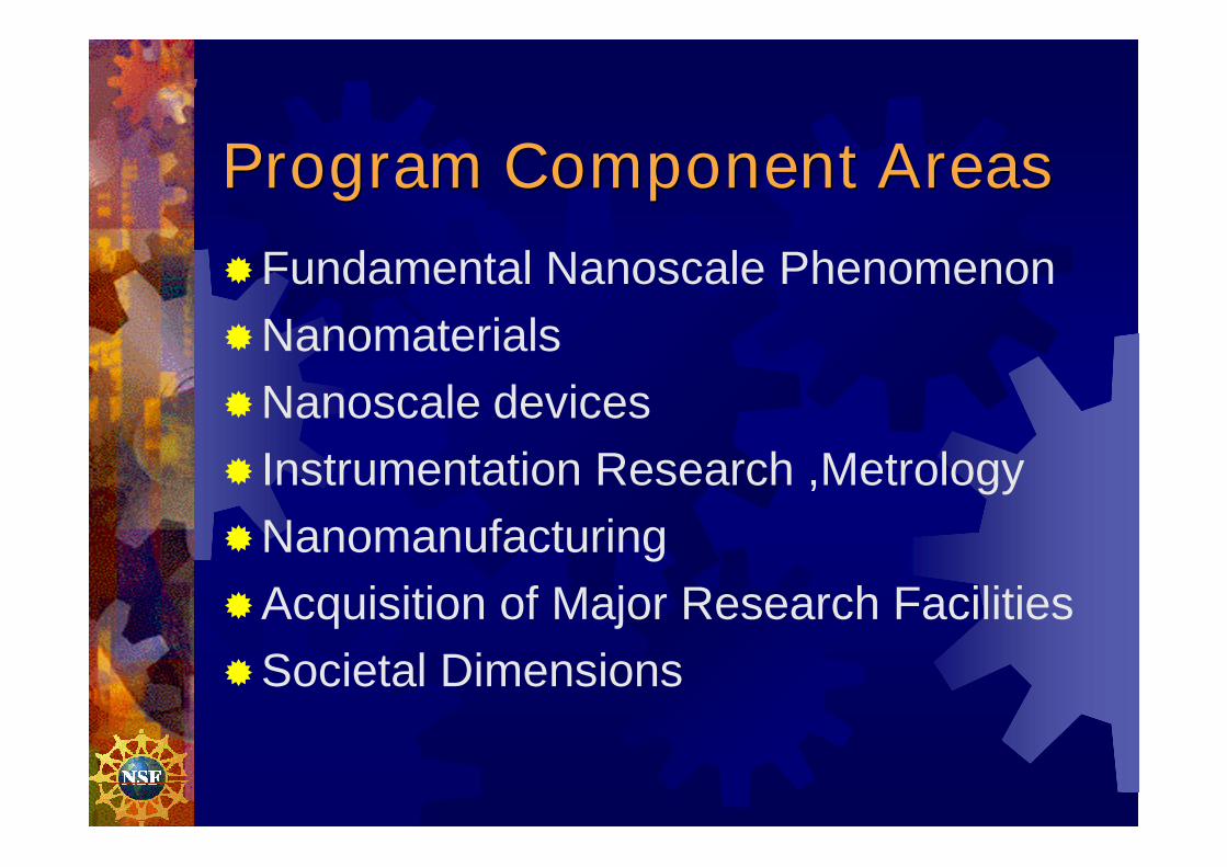
Program Component AreasProgram Component AreasFundamental Nanoscale PhenomenonNanomaterialsNanoscale devicesInstrumentation Research ,MetrologyNanomanufacturingAcquisition of Major Research FacilitiesSocietal Dimensions

Industry Liaison in SupportIndustry Liaison in Supportof Technology Transfer andof Technology Transfer andCommercializationCommercialization
Chemical IndustrySemiconductor/Electronics IndustryIndustrial Research InstituteSBIR/STTR programs

Small Business InnovationSmall Business InnovationResearch/Small BusinessResearch/Small BusinessTechnology TransferTechnology Transfer(SBIR/STTR) Program at the(SBIR/STTR) Program at theNational Science FoundationNational Science Foundation

DODDOD DefenseDefense HHSHHS HealthHealth NASANASA SpaceSpace DOEDOE EnergyEnergy NSFNSF ~$104Million~$104Million DHSDHS HomeLandHomeLand SecuritySecurity USDAUSDA AgricultureAgriculture DOCDOC CommerceCommerce EPAEPA EnvironmentEnvironment DOTDOT TransportationTransportation DoEDDoED EducationEducation
Participating AgenciesParticipating Agencies
TOTAL ~TOTAL ~ $2.0B$2.0BEst. FY 2004Est. FY 2004

Topics Supported at NSFTopics Supported at NSFElectronicsAdvanced MaterialsBiotechnologyInformation TechnologySpecial Topics
Manufacturing InnovationSecurity Technologies

NSF SBIR/STTR Innovation ModelNSF SBIR/STTR Innovation Model
PHASE IIIProduct
Development toCommercial
Market
PHASE IFeasibilityResearch
$100k/6 mos
TaxesFederal Investment
PHASE IIResearchtowards
Prototype$500k/24 mos
MATCHMAKER
Phase IIBThird-Party
Investment +1:2 NSF
Matching
Private Sector orNon-SBIRInvestmentUnique to NSF

Phase I Feasibility Research – ~10-15% successrate at NSF SBIR – 6 months – up to $100,000 STTR – 12 months – up to $100,000
Phase II – Concept Development – ~30-40%success rate at NSF SBIR/STTR – 24 months up to $500,000
Phase IIB unique to NSF – Matches Third PartyInvestmentNSF - $50,000 to $500,000 Investor - $100,000 to $1,000,000
Phase III – Commercial Application PrivateFunding
NSF SBIR/STTR PhasedNSF SBIR/STTR PhasedProject StructureProject Structure

Nanotechnology Thrusts inNanotechnology Thrusts inSBIR/STTR at NSFSBIR/STTR at NSF
Synthesis and ProcessingSynthesis and Processing - techniques forsynthesis, fabrication, and processing ofnanostructures
Materials, Devices, Systems, and ArchitecturesMaterials, Devices, Systems, and Architectures -techniques for processing and converting moleculesand nanoprecursors into functional nanostructures;nanostructured materials, nanocomponents andnanodevices
NanomanufacturingNanomanufacturing - techniques for synthesis andscale-up of structures, devices and systemsemploying nanostructured materials and processeswith nanoscale control

NSF SBIR/STTR Grants inNSF SBIR/STTR Grants inNANOTECHNOLOGY in MillionsNANOTECHNOLOGY in Millionsof Dollars from FY1999 toof Dollars from FY1999 toFY2005FY2005
0
2
4
6
8
10
12
14
16
1999 2000 2001 2002 2003 2004 2005
Phase I/II
Inve
stm
ent(
$mm
)

Nanoparticle compositesNanofilter membranesNanocrystalline coatingsNanobiomaterialsNanoelectronicsNanophotonicsNanomagneticsNanomanufacturing
Major Product AreasMajor Product AreasFundedFunded

NanoparticleNanoparticle compositescomposites

Eltron Research IncEltron Research IncRichard A. BleyRichard A. Bley
Incorporation of CarbonNanotubes Into Nylon Filaments
Technical Objective• Formulate Synthesis For Making
Functionalized Polymer That Wraps SWNT• Develop Viable Functional Groups• Develop Methods For Making Composites• Determine Mechanical, Electrical and
Thermal Properties
Goals• To Incorporate SWNTs Into Nylon Filaments• To Make Very Strong, Light Weight
Structural Materials Using This PolymerComposite
• To Make Electrically and ThermallyConductive Composites For Use In EMIShielding And As Adhesives
Commercialization Strategy• Patent ApplicationU.S. Provisional Application Serial No.60/497,896.U.S Patent Application Serial No. 10/927,628.
• Have Interested Corporation (Henkel) ButStill Need to Demonstrate Method ProducesDesired Properties in Composites
0716rab1.dsf

Reactive NanotechnologiesReactive NanotechnologiesTim Weihs & Jai SubramanianTim Weihs & Jai Subramanian
Commercialization StrategyMarket strategy: engage end-users and
partner with established companies in theadjacent markets: solders, adhesives, etc.
Reach broader market by: Leveraging performance and reliability data
results from the grant work. Leveraging capabilities in shaping foils,
ignition methods and foil-solder pre-forms Aligning closely with market enablers like
sub-con. assemblers and thermalmanagement solution providers.
GoalsHeat sink to die/spreader optimization andcharacterization. Determine optimal configuration for heat sink
mounting. (April 2004) Optimize thermal performance of above
configuration. (October 2004) Optimize and characterize performance of
heat sink to silicon joints. (April 2005) Gather long term reliability data and complete
characterization efforts. (October 2005)
Technical Objectives1. Select configuration for mounting heat
sinks to dies/spreaders.2. Optimize configuration for best thermal
performance and ease of commercialinsertion.
3. Characterize configuration to demonstratereliability and repeatability.
Reactive Mounting of Heat Sinks
Pre-wetSolder
SiliconDieHeat Spreader
HeatSinkReactive
Foil
ChipPackage

NanofilterNanofilter membranesmembranes

eSpinHigh Efficiency Nanofilter Media
Technology:Nanofiber from
Solution Spinning technologyWeb manufacture
SBIR Follow-On Funding: FleetGuard Diesel
Filter State of Tennessee

NanocrystallineNanocrystalline coatingscoatings

Vista Engineering Inc.Vista Engineering Inc.Raymond G. ThompsonRaymond G. ThompsonDMIDMI--03497690349769
Nanocrystalline DiamondCoated Cutting Tools
Technical Objectives
Goals Commercialization Strategy
High-endHigh ProductivityPartner with Tool ManufacturerAutomotive Applications
Batch ProcessIntrinsic Film AdhesionRobust Process Parameters
Product to Market 2005Venture Capital 2004 – 2005Win in Growing Market -
$300M in 2010

ALD NanoSolutions, Inc.ALD NanoSolutions, Inc.Dr. Karen J.Dr. Karen J. BuechlerBuechlerDMIDMI--04222200422220
STTR Phase II: Novel NanocoatedFerromagnetic Materials
Technical Objectives:
Goals: Commercialization Strategy:•Use Particle-ALD™ to Deposit Nanothick Filmson Fine Particles
•Develop Pilot Scale Production Capabilities forParticle-ALD™
•Develop Link to Consumer Products forNanocoated Fine particles through use ofStrategic Partners
•Develop Atomic Layer Deposition (ALD) chemistry forplacing conformal, pinhole-free, and nanothick aluminafilms on individual primary particles
•Produce Kilograms of nanocoated fine iron powdersusing a scaleable fluidized bed process
•Characterize the product: film thickness, composition,crystallinity, particle size distribution, surface area,oxidation resistance, magnetic moment
•Work with Strategic Partners to Design materials forthe Aerospace, Elecronic, and Automotive Industries
•Using Facilities proven during Phase II, providematerials for Consumer Product Development
•License or Manufacture coated particles designedthrough Phase II to Strategic Partners as needs dictate
-Al2O3growingepitaxiallyto ironparticlesurface

NanobiomaterialsNanobiomaterials

Luna InnovationsLuna InnovationsCharlie PenningtonCharlie Pennington
“Nuclear-Magnetic Resonance(NMR) Properties of CarbonNanomaterials for MedicalApplications”
Technical Objectives
• Enhance Production Efficiency forGd3N@C80 and other Trimetaspheres
• Optimize and Finalize functionalizationof Gd3N@C80
• Optimize and functionalize Er3N@C80,Ho3N@C80, and Tb3N@C80
Goals• Increase production efficiency by 10X
• Enhance water solubility whilemaintaining low apparent molecularweight
• Develop high field strength MRIcontrast agents
Commercialization Strategy• Competitive advantage-25X moresensitive than current MRI agents
• Establish wide customer base salesthrough emerging and establishedpharmaceutical companies
• Ability to produce “site-directed”contrast agents

Dr. Stuart FarquharsonDr. Stuart FarquharsonNanomaterialNanomaterial for Microchip Sensorsfor Microchip Sensors
Providing Chemical Information When & Where You Need It
Goal
Build a microchip chemical analyzer thatsimultaneously separates chemicalspecies and provides surface-enhancedRaman activity to allow < 5-min analysisof < mL samples at ppm concentrations.
Commercialization Strategy
• Protect with patents(two submitted 10/02, third in 01/03)
• Develop applications with strategicpartners (pharmaceutical, medical, clinical,biotech)• Leverage exclusive use against investment
Technical Objectives
• Develop Separation Chemistry• Design & Build SERS Microchip• Build Analyzer (fluid delivery)• Test Analyzer (figures of merit)• Product Design with Customers
ResultsTo Date
Applied Spectroscopy, 57, 479 (2003)Wavenumber (cm-1)
phenyl acetylene
p-aminobenzoic acid3-min
2 chemicalsseparated andidentified in 3-min

Nomadics, IncNomadics, IncLawrence F. Hancock andLawrence F. Hancock and JoonghoJoonghoMoonMoon
Fluorescent Polymer Nanoparticles
Commercialization Strategy
GeneExpressionReagents
q-RT PCRReagents
• Optimize PPE Nanoparticles• Demonstrate PPE Fluorescence Quenching
Enhancement• Gene Expression & q-PCR Reagents
Define Specifications and PerformanceCompare Specs. And Performance with CompetitorsSOP’s and QA/QC ProceduresProtocolsBeta TestDraft Instructions/Application Notes
Technical Objectives617-441-8871,[email protected]
215 First St., Suite 104,Cambridge, MA 02142
Goals• Direct integration of PPE nanoparticles
into widely practiced experiments onexisting bioanalytical instrumentplatforms.
• Introduction of PPE-based labels andnucleotide conjugates in application-specific reagent kits.
• License and/or partner with establishedreagent suppliers and equipmentmanufacturers.
• Develop and LaunchGene Expression Reagentsq-RT PCR Reagents
“Improved Photostability”“Enhanced Sensitivity”“Wide Dynamic Range”

NanoelectronicsNanoelectronics

Nanosys Inc.Nanosys Inc.Erik ScherErik ScherDMIDMI--04221470422147
Nanocomposite Solar Cells Technical Objectives:
• Develop optically and electroniclyenhanced nanocrystals• Develop new Device Components• Develop Advanced DeviceArchitectures
Goal:• Develop high performance, low costlightweight flexible solar cells
Approach:• Innovative solar cell design thatcombines precisely engineered inorganicsemiconductor nanocrystals with a light-weight, flexible host-matrix
Commercialization Strategy:
• Nanosys focuses on nanotechnologyelement in the end product• Partner with industry leaders to jointlydevelop and manufacture nano-enabledcomponent into end product.• Our partner provides marketingresources and access to end customers
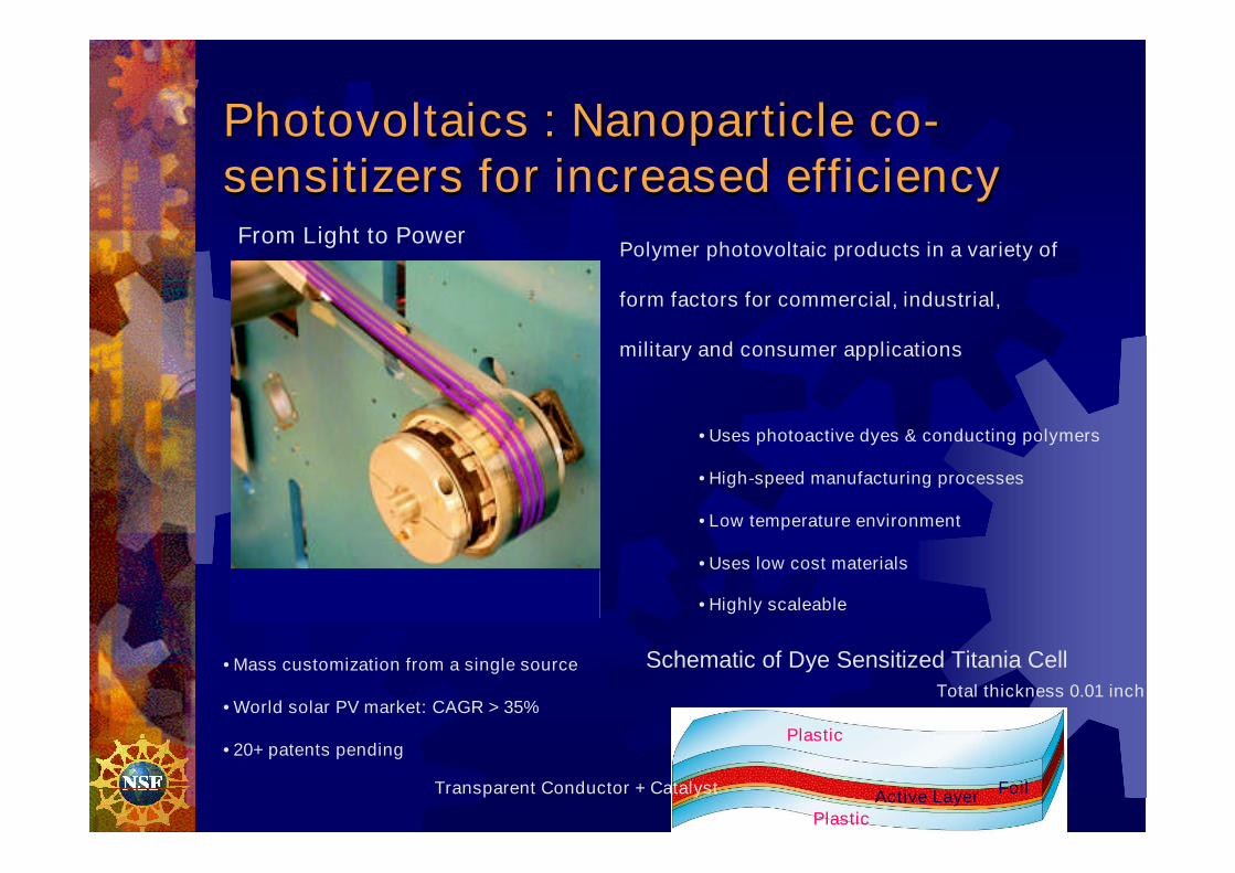
PhotovoltaicsPhotovoltaics :: NanoparticleNanoparticle coco--sensitizers for increased efficiencysensitizers for increased efficiency
From Light to PowerPolymer photovoltaic products in a variety of
form factors for commercial, industrial,
military and consumer applications
Plastic
FoilActive LayerTransparent Conductor + Catalyst
Plastic
Total thickness 0.01 inch• Mass customization from a single source
• World solar PV market: CAGR > 35%
• 20+ patents pending
• Uses photoactive dyes & conducting polymers
• High-speed manufacturing processes
• Low temperature environment
• Uses low cost materials
• Highly scaleable
Schematic of Dye Sensitized Titania Cell

Thin Film Transistors:Thin Film Transistors:SiliconSilicon NanowiresNanowires
High Performance, large area nano-structured macro-electronics substrate technology
TFT Backplane Drivers – Integrated EdgeElectronics
Beam-Steering Antennas
RFID Tags
• Eliminates high-temperature steps required for semiconductordeposition
• Dramatically reduces manufacturing cost, time and complexity
• Deposition on virtually any substrate material possible
A variety of application areas:
• Portable & large-area flat panel displays
• Low-cost RFID and smart cards
•Electronically steerable phased-array RF antennas

nanophotonicsnanophotonics
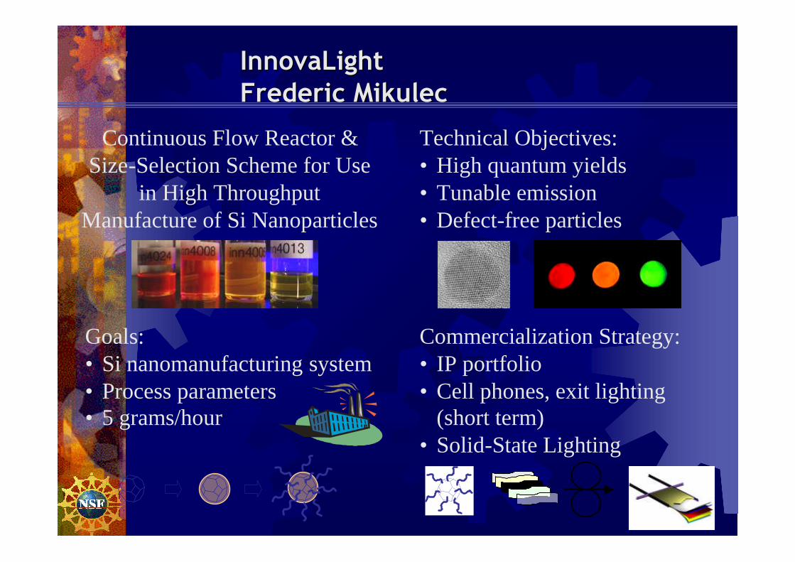
InnovaLightInnovaLightFredericFrederic MikulecMikulec
Continuous Flow Reactor &Size-Selection Scheme for Use
in High ThroughputManufacture of Si Nanoparticles
Technical Objectives:• High quantum yields• Tunable emission• Defect-free particles
Goals:• Si nanomanufacturing system• Process parameters• 5 grams/hour
Commercialization Strategy:• IP portfolio• Cell phones, exit lighting
(short term)• Solid-State Lighting
Mfgr's rep

SemiconductorSemiconductor NanocrystalNanocrystal (Quantum Dot) Manufacturing(Quantum Dot) Manufacturing
A New Scale-Up Technology forIndustrial Production of High-Quality
Semiconductor Nanocrystals
Technical Objectives
• Develop large-scale synthetic protocols fortype II-IV, III-V, IV-VI semiconductornanocrystals
• Stabilize these nanocrystals with dendronligands
• Establish industrial standards
• Assemble Auto CB SynthesizerTM2.5 nm CdSe 3.5 nm CdSe 5.5 nm CdSe
Commercialization strategy
• Highest Quality: stable, surface flexibility, narrowsize distribution
• Lowest Price: affordable
• Broadest Range: II-IV, III-V, and IV-VIsemiconductor nanocrystals
NN-Labs will offer customers colloidalsemiconductor nanocrystals with the:
Goals:
• Focus on electronic and biological applications
• Patent and license the synthesis protocol
• Advertise: Commercial ads and conferenceexhibits
• Secure financial support from VC and strategicpartners

NanomagneticsNanomagnetics

NanoNano--magnetic materialsmagnetic materials
Nanocrystalline FeCo forEMI Suppression
Technical Objectives• Production of nano-sized FeCo and their
consolidation to near net shapes• Magnetic Characterization and EMI
testing• Fabrication of magnetic bearings and
their testing• Fabrication of materials for inductors and
their testing
Goals• Scale up the production and the
consolidation process• Tailor materials for EMI suppression
up to 1 GHz• Optimize material properties for
enhanced bearing performance inflywheel energy storage and artificialimplants
• Low loss magnetic cores and inductors
Commercialization Strategy• Strategic Alliances• Worldwide licensing for a fixed fee• Spin off a separate business unit

NanomanufacturingNanomanufacturing