the triscend configurable system interconnect (csi) bus … · 2010-05-06 · configurable system...
TRANSCRIPT

Page 1, 20-JUL-1999
The Configurable System-on-Chip Company
The Triscend E5 Configurable System
Interconnect (CSI) BusJuly 1999
© 1999 by Triscend Corporation. All rights reserved.

Page 2, 20-JUL-1999
Agenda
The BasicsAddress SelectorsConverting an Existing 8032 DesignCreating Address StructuresDMA OperationsThe CSI Bus Simulation ModelWait-State and BreakpointSummary and Questions
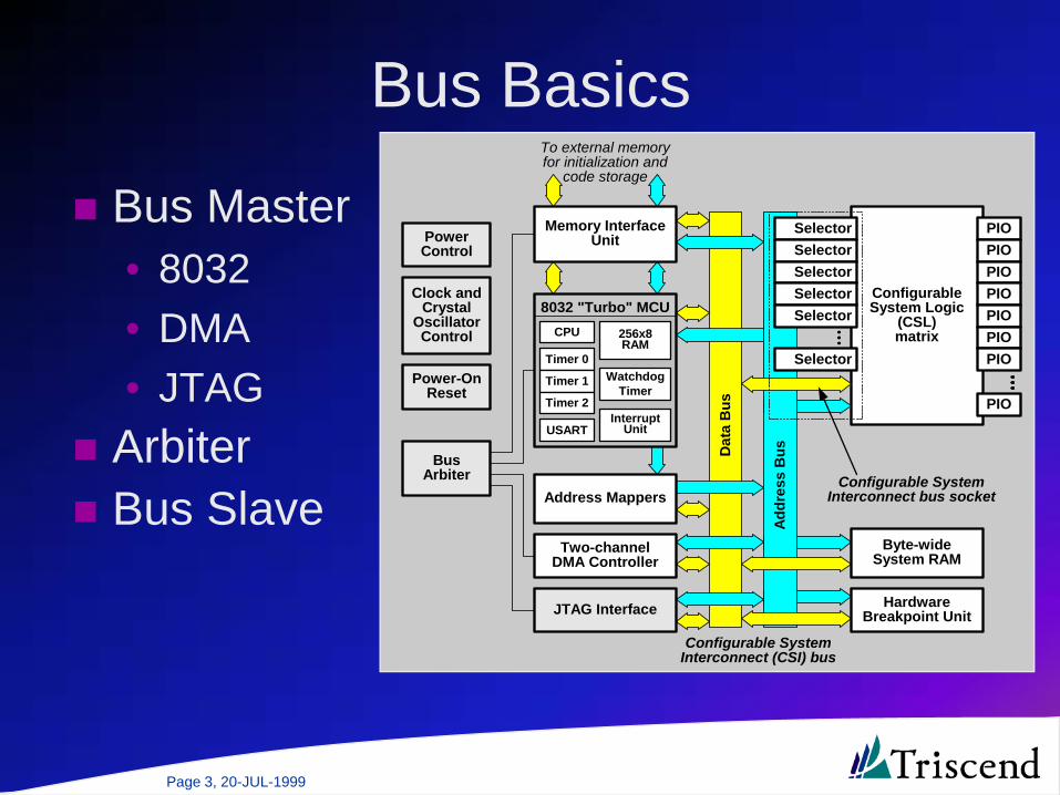
Page 3, 20-JUL-1999
Bus Basics
Bus Master• 8032• DMA• JTAG
ArbiterBus Slave
ConfigurableSystem Logic
(CSL)matrix
PIOPIOPIOPIOPIO
BusArbiter
PowerControl
Addr
ess
Bus
SelectorSelector
Dat
a B
us
Clock andCrystal
OscillatorControl
Power-OnReset
To external memoryfor initialization and
code storage
Configurable SystemInterconnect (CSI) bus
Configurable SystemInterconnect bus socket
CPU
USART
WatchdogTimer
InterruptUnit
256x8RAM
Timer 0
Timer 1
Timer 2
8032 "Turbo" MCU
Selector
SelectorSelector
Address Mappers
Two-channelDMA Controller
JTAG Interface
Byte-wideSystem RAM
HardwareBreakpoint Unit
Memory InterfaceUnit
Selector
PIO
PIOPIO
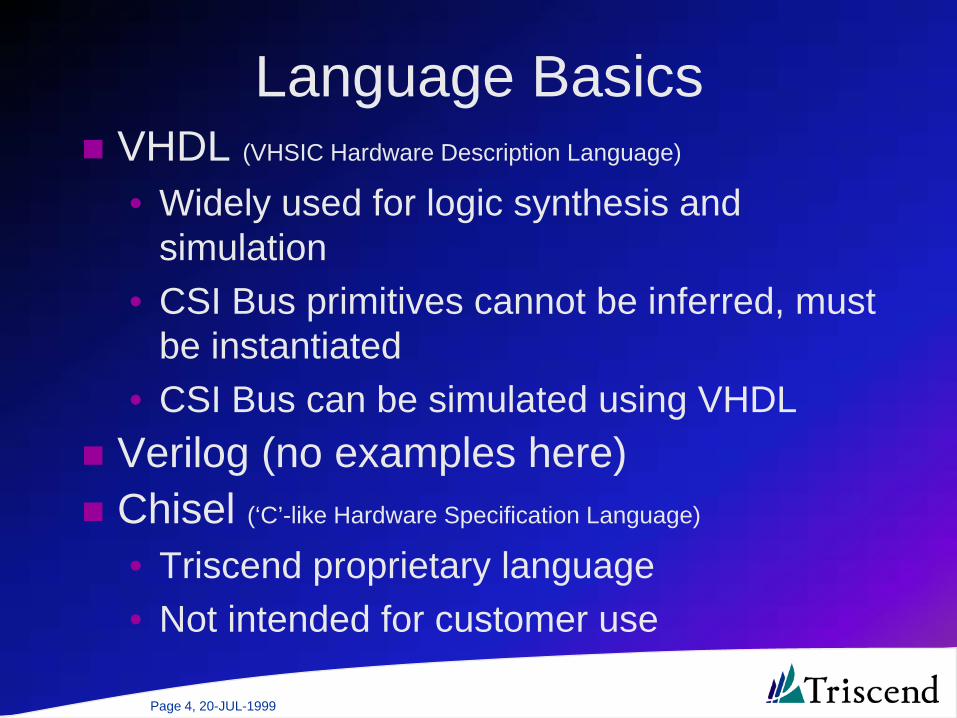
Page 4, 20-JUL-1999
Language BasicsVHDL (VHSIC Hardware Description Language)
• Widely used for logic synthesis and simulation
• CSI Bus primitives cannot be inferred, must be instantiated
• CSI Bus can be simulated using VHDLVerilog (no examples here)Chisel (‘C’-like Hardware Specification Language)
• Triscend proprietary language• Not intended for customer use

Page 5, 20-JUL-1999
CSI Bus Basics
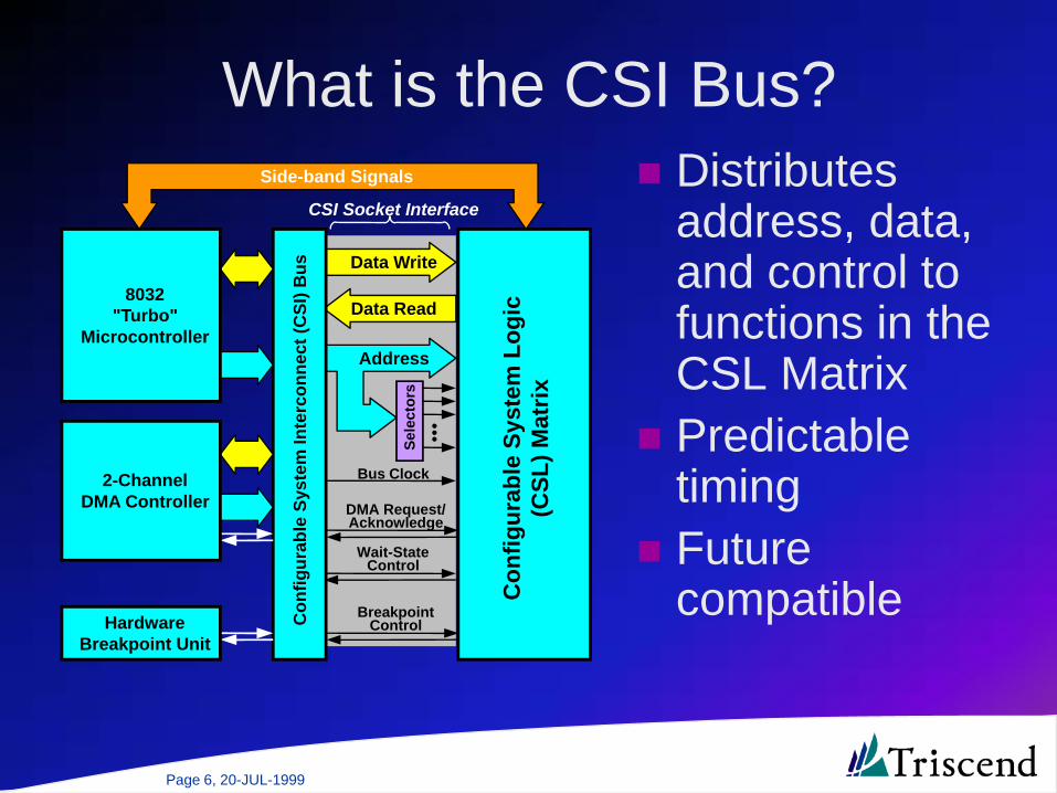
Page 6, 20-JUL-1999
CSI Socket Interface
Data Write
Data Read
Address
Sele
ctor
s
Bus Clock
Wait-StateControl
Con
figur
able
Sys
tem
Inte
rcon
nect
(CSI
) Bus
Con
figur
able
Sys
tem
Log
ic
(CSL
) Mat
rix
8032"Turbo"
Microcontroller
What is the CSI Bus?Distributes address, data, and control to functions in the CSL MatrixPredictable timingFuture compatible
Side-band Signals
BreakpointControlHardware
Breakpoint Unit
DMA Request/Acknowledge
2-ChannelDMA Controller

Page 7, 20-JUL-1999
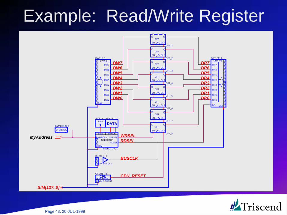
Example: Read/Write Register
SIM[127..0]
DR4
DW1
BUSCLK
DW2DW3
DR7DW6DW7
CPU_RESET
DR5DW5
WRSEL
DR0
DW4
RDSEL
DR1
DR6
DR2
DW0
DR3
D
EN
Q
CLRDFF_6
DFF
BU
S
SIM
DR0
DR1
DR2
DR3
DR4
DR5
DR6
DR7
EN
DR7_0E_1DR7_0E
SIM
BUSCLK_1
BUSCLK
D
EN
Q
CLRDFF_1
DFF
SIZE SPACE
SIM
SYMBOLIC WRSEL
RDSEL
SELECTOR_1
SELECTOR
DATASPACE_1
BU
S
SIMDW0
DW1
DW2
DW3
DW4
DW5
DW6
DW7
DW7_0_1DW7_0
D
EN
Q
CLRDFF_7
DFF
D
EN
Q
CLRDFF_4
DFF
D
EN
Q
CLRDFF_5
DFF
D
EN
Q
CLRDFF_8
DFF
D
EN
Q
CLRDFF_3
DFF
SIZE
1
SIZE_1
D
EN
Q
CLRDFF_2
DFF
SYMBOLICSYMBOLIC_1
SIM
CPUWAS RESET
CPURST_1
CPURST
MyAddress
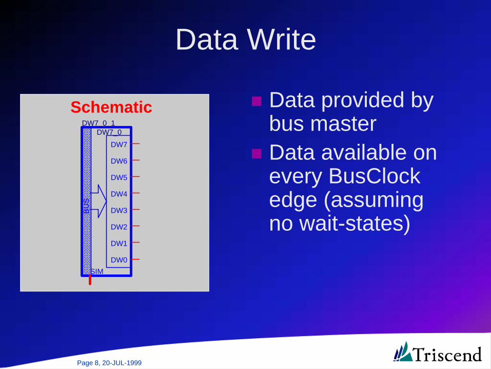
Page 8, 20-JUL-1999
Schematic
Data Write
Data provided by bus masterData available on every BusClock edge (assuming no wait-states)
BU
S
SIMDW0
DW1
DW2
DW3
DW4
DW5
DW6
DW7
DW7_0_1DW7_0
Page 9, 20-JUL-1999
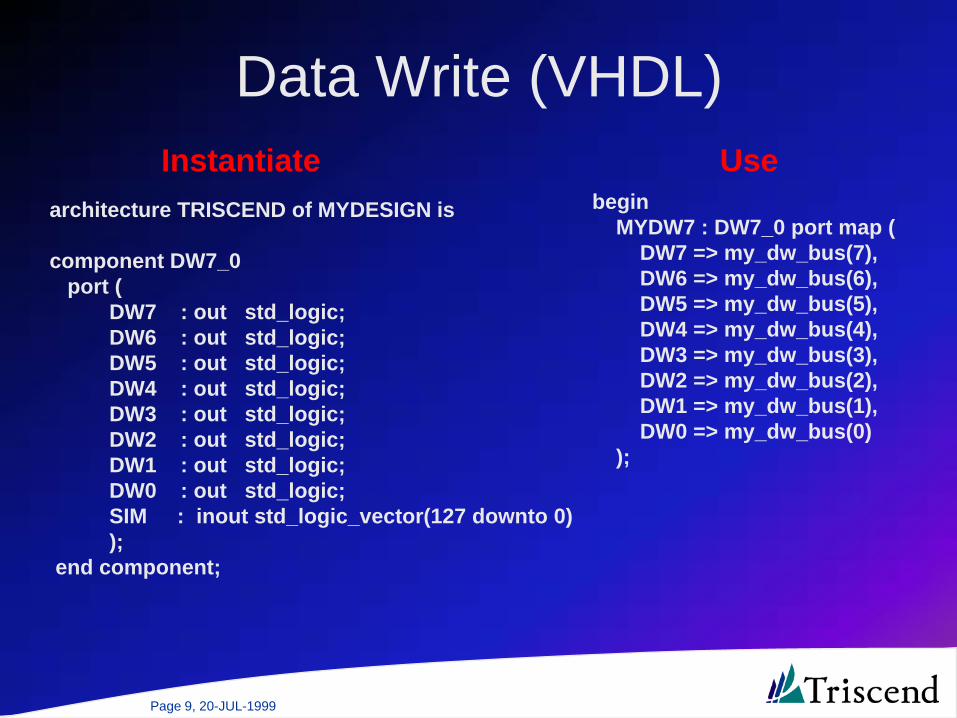
Data Write (VHDL)
architecture TRISCEND of MYDESIGN is
component DW7_0port (
DW7 : out std_logic;DW6 : out std_logic;DW5 : out std_logic;DW4 : out std_logic;DW3 : out std_logic;DW2 : out std_logic;DW1 : out std_logic;DW0 : out std_logic;SIM : inout std_logic_vector(127 downto 0));
end component;
beginMYDW7 : DW7_0 port map (
DW7 => my_dw_bus(7),DW6 => my_dw_bus(6),DW5 => my_dw_bus(5),DW4 => my_dw_bus(4),DW3 => my_dw_bus(3),DW2 => my_dw_bus(2),DW1 => my_dw_bus(1),DW0 => my_dw_bus(0)
);
Instantiate Use
Page 10, 20-JUL-1999
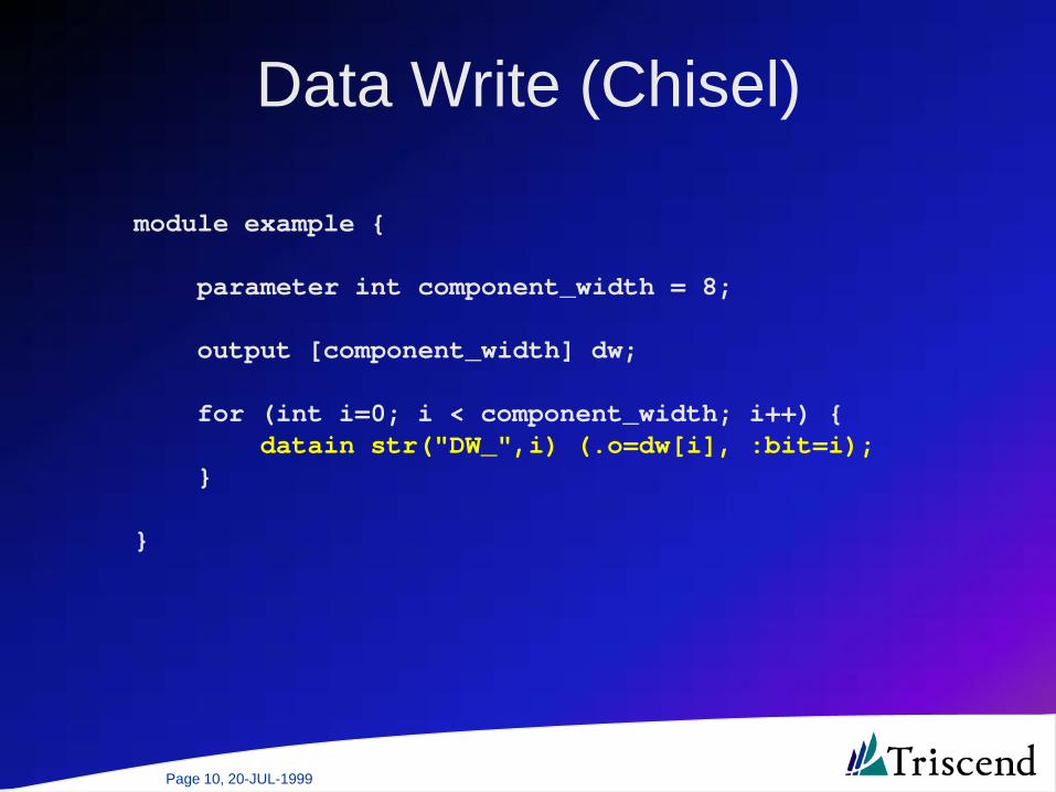
Data Write (Chisel)
module example {
parameter int component_width = 8;
output [component_width] dw;
for (int i=0; i < component_width; i++) {datain str("DW_",i) (.o=dw[i], :bit=i);
}
}
Page 11, 20-JUL-1999
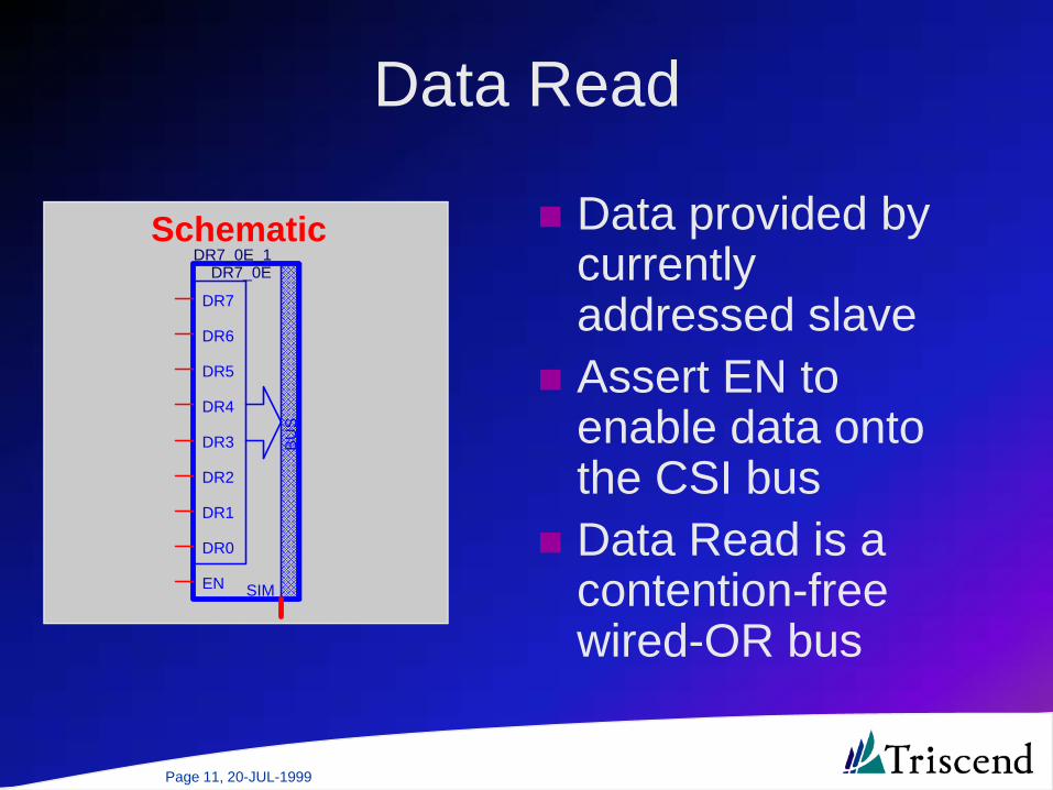
Data Read
SchematicB
US
SIM
DR0
DR1
DR2
DR3
DR4
DR5
DR6
DR7
EN
DR7_0E_1DR7_0E
Data provided by currently addressed slaveAssert EN to enable data onto the CSI busData Read is a contention-free wired-OR bus
Page 12, 20-JUL-1999
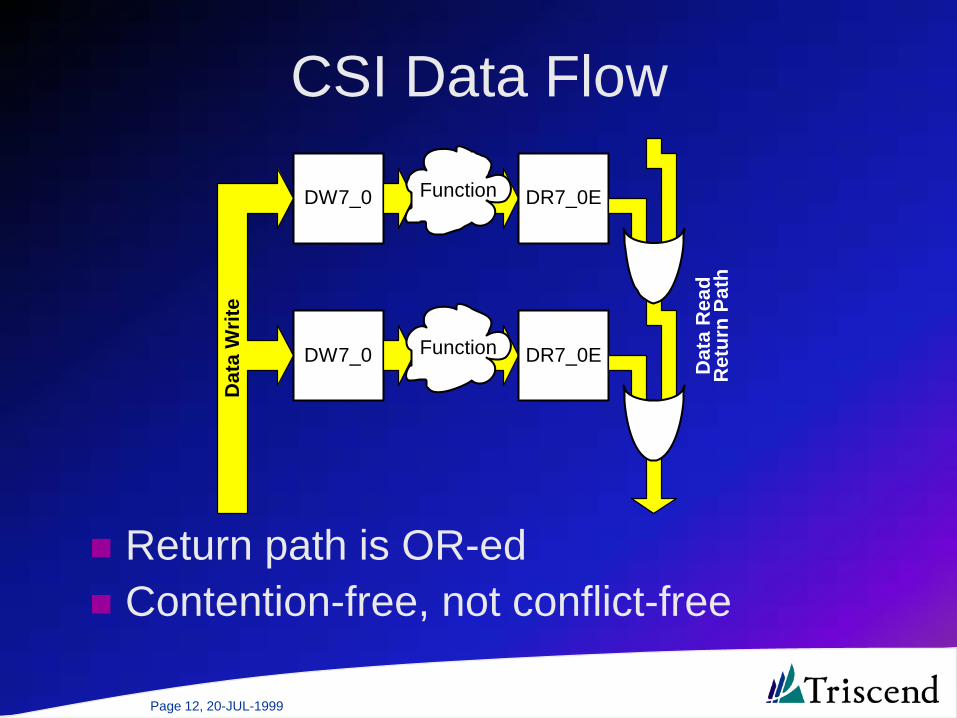
CSI Data Flow
Return path is OR-edContention-free, not conflict-free
DW7_0 Function DR7_0E
DW7_0 Function DR7_0E
Dat
a W
rite
Dat
a R
ead
Ret
urn
Path
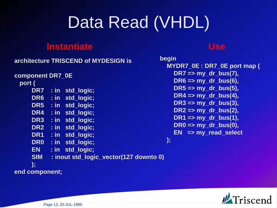
Page 13, 20-JUL-1999
architecture TRISCEND of MYDESIGN is
component DR7_0Eport (
DR7 : in std_logic;DR6 : in std_logic;DR5 : in std_logic;DR4 : in std_logic;DR3 : in std_logic;DR2 : in std_logic;DR1 : in std_logic;DR0 : in std_logic;EN : in std_logic;SIM : inout std_logic_vector(127 downto 0));
end component;
Data Read (VHDL)
beginMYDR7_0E : DR7_0E port map (
DR7 => my_dr_bus(7),DR6 => my_dr_bus(6),DR5 => my_dr_bus(5),DR4 => my_dr_bus(4),DR3 => my_dr_bus(3),DR2 => my_dr_bus(2),DR1 => my_dr_bus(1),DR0 => my_dr_bus(0),EN => my_read_select
);
Instantiate Use
Page 14, 20-JUL-1999
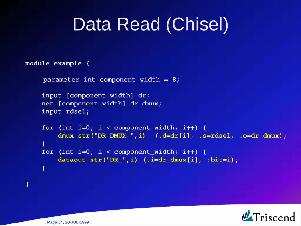
Data Read (Chisel)
module example {
parameter int component_width = 8;
input [component_width] dr;net [component_width] dr_dmux;input rdsel;
for (int i=0; i < component_width; i++) {dmux str("DR_DMUX_",i) (.d=dr[i], .s=rdsel, .o=dr_dmux);
}for (int i=0; i < component_width; i++) {
dataout str("DR_",i) (.i=dr_dmux[i], :bit=i);}
}
Page 15, 20-JUL-1999
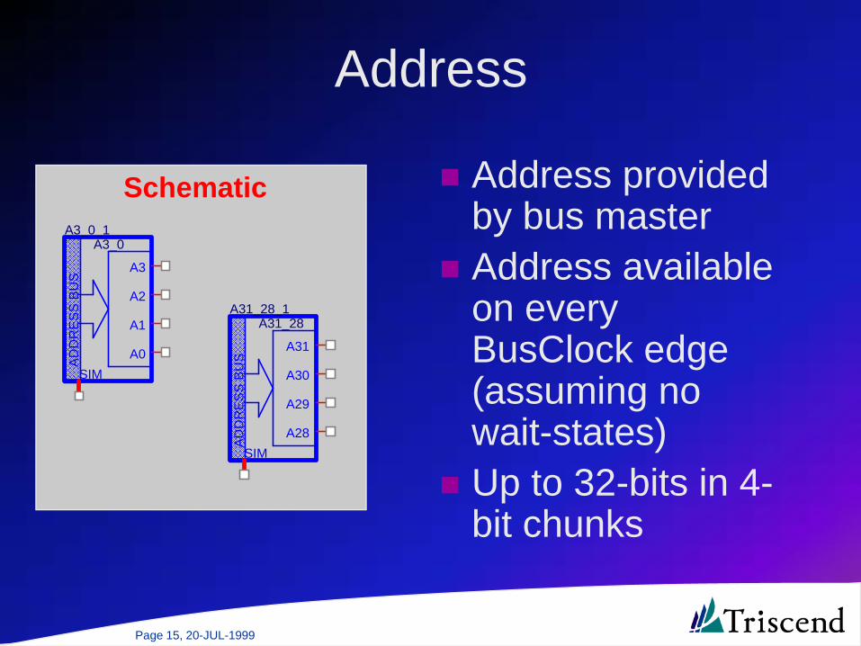
Address
Schematic
AD
DR
ES
S B
US
A3
A2
A1
A0SIM
A3_0_1A3_0
AD
DR
ES
S B
US
A31
A30
A29
A28SIM
A31_28_1A31_28
Address provided by bus masterAddress available on every BusClock edge (assuming no wait-states)Up to 32-bits in 4-bit chunks

Page 16, 20-JUL-1999
Address (VHDL)
beginMYA3_0 : A3_0 port map (
A3 => my_addr(3),A2 => my_addr(2), A1 => my_addr(1),A0 => my_addr(0)
);
Instantiate Usearchitecture TRISCEND of MYDESIGN is
component A3_0port (
A3 : out std_logic;A2 : out std_logic;A1 : out std_logic;A0 : out std_logic;SIM : inout std_logic_vector(127 downto 0));
end component;
A31_28A27_24A23_20A19_16
A15_12A11_8A7_4A3_0
Available Components
Page 17, 20-JUL-1999
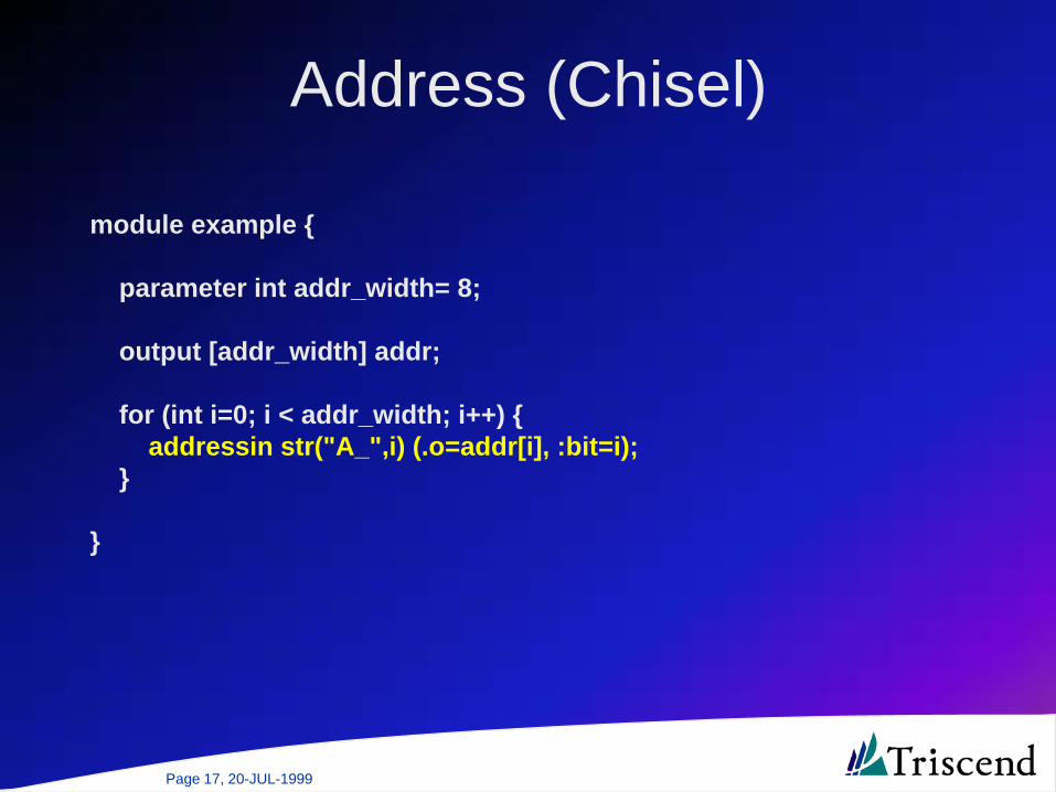
Address (Chisel)
module example {
parameter int addr_width= 8;
output [addr_width] addr;
for (int i=0; i < addr_width; i++) {addressin str("A_",i) (.o=addr[i], :bit=i);
}
}
Page 18, 20-JUL-1999
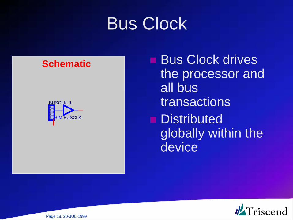
Bus Clock
Schematic Bus Clock drives the processor and all bus transactionsDistributed globally within the device
SIM
BUSCLK_1
BUSCLK

Page 19, 20-JUL-1999
Bus Clock (VHDL)
architecture TRISCEND of MYDESIGN is
component BUSCLKport (
O : out std_logic;SIM : inout std_logic_vector(127 downto 0));
end component;
beginMYBUSCLK : BUSCLK port map (
O => my_local_clock);
Instantiate Use
Bus Clock (Chisel)module example {
output my_local_clock;busclk (.o=my_local_clock);
}
Page 20, 20-JUL-1999
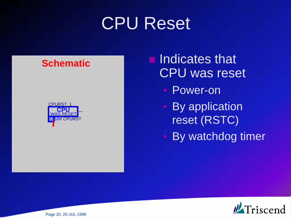
CPU Reset
Schematic Indicates that CPU was reset• Power-on• By application
reset (RSTC)• By watchdog timer
SIM
CPUWAS RESET
CPURST_1
CPURST
Page 21, 20-JUL-1999
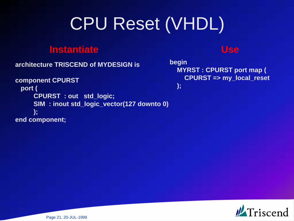
CPU Reset (VHDL)
architecture TRISCEND of MYDESIGN is
component CPURSTport (
CPURST : out std_logic;SIM : inout std_logic_vector(127 downto 0));
end component;
beginMYRST : CPURST port map (
CPURST => my_local_reset);
Instantiate Use

Page 22, 20-JUL-1999
CPU Reset (Chisel)
module example {
output my_reset;
cpurst (.cpurst=my_reset);
}

Page 23, 20-JUL-1999
Address Selectors
Page 24, 20-JUL-1999
What is an Address?
Three types of addresses for the E5• 8032 “Logical” address (16-bits, 64K)• E5 “Physical” address (32-bits, 4G)
• 8032’s 64K address spaces are mapped into regions of the 4G physical address space
• The E5’s mappers translate the 8032’s logical address into an E5 physical address
• Technology-independent “Symbolic” address• Re-useable, “plug and play” approach
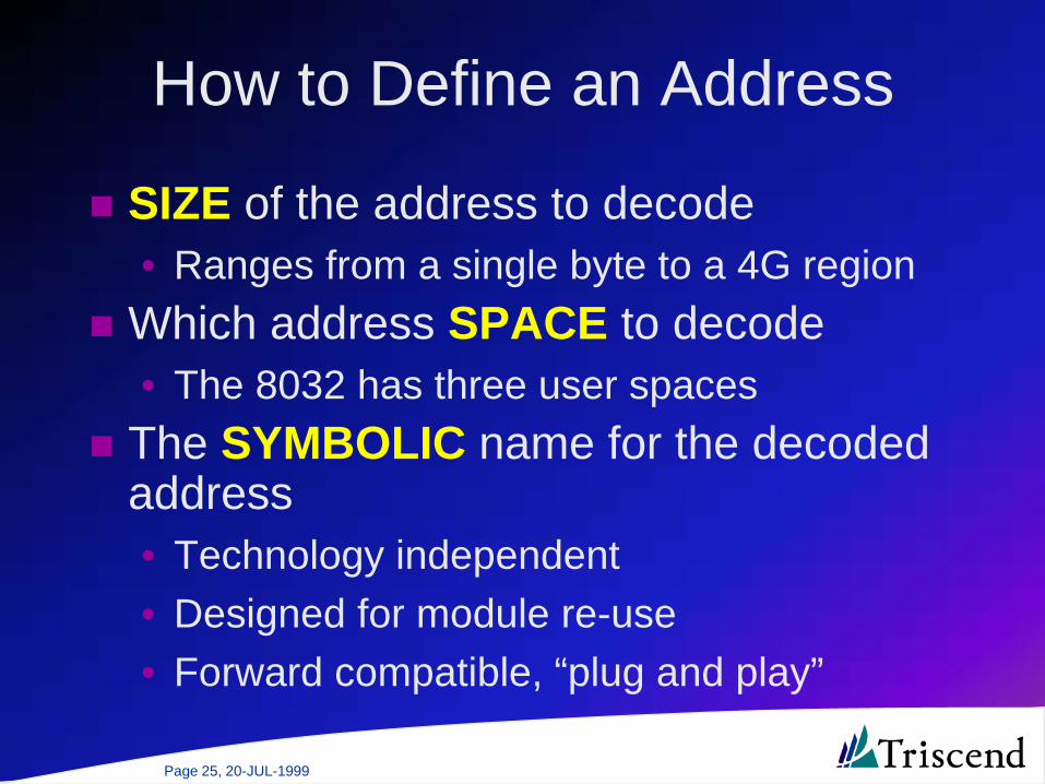
Page 25, 20-JUL-1999
How to Define an Address
SIZE of the address to decode• Ranges from a single byte to a 4G region
Which address SPACE to decode• The 8032 has three user spaces
The SYMBOLIC name for the decoded address• Technology independent• Designed for module re-use• Forward compatible, “plug and play”
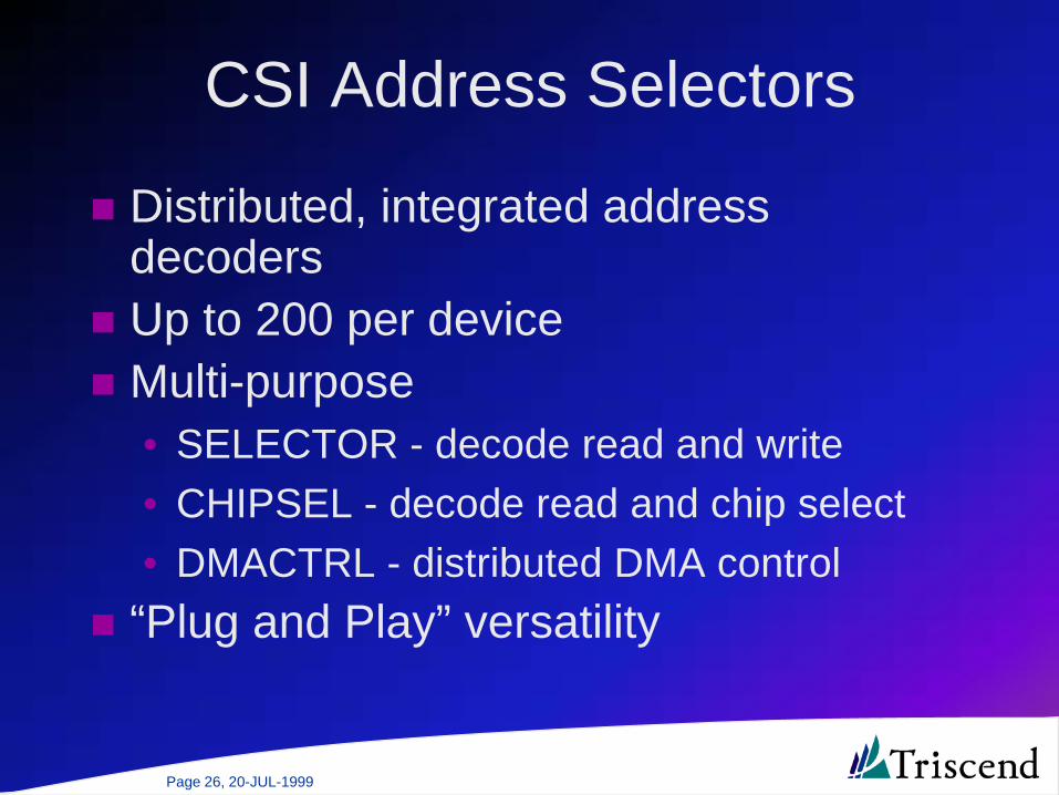
Page 26, 20-JUL-1999
CSI Address Selectors
Distributed, integrated address decodersUp to 200 per deviceMulti-purpose• SELECTOR - decode read and write• CHIPSEL - decode read and chip select• DMACTRL - distributed DMA control
“Plug and Play” versatility

Page 27, 20-JUL-1999
Selector
Separately decode read and write transactionsUse SELECTORW if you need a wait-state
Schematic
DATASPACE_1
SIZE SPACE
SIM
SYMBOLIC WRSEL
RDSEL
SELECTOR_1
SELECTOR
SIZE
1
SIZE_1

Page 28, 20-JUL-1999
Selector (Hardware)
Match0
Match1
A31
A0A1A2
CSI Bus Address
RDSEL
WRSEL
READ
WRITE
BUSCLK

Page 29, 20-JUL-1999
Selector Programming Example
Match1 Match0 Purpose0 0 Disabled0 1 An=11 0 An=01 1 Don’t care
Each address bit individually decoded• Match on High• Match on Low• Match on either
(don’t care)Final decode is the AND of all 32 lines
Page 30, 20-JUL-1999
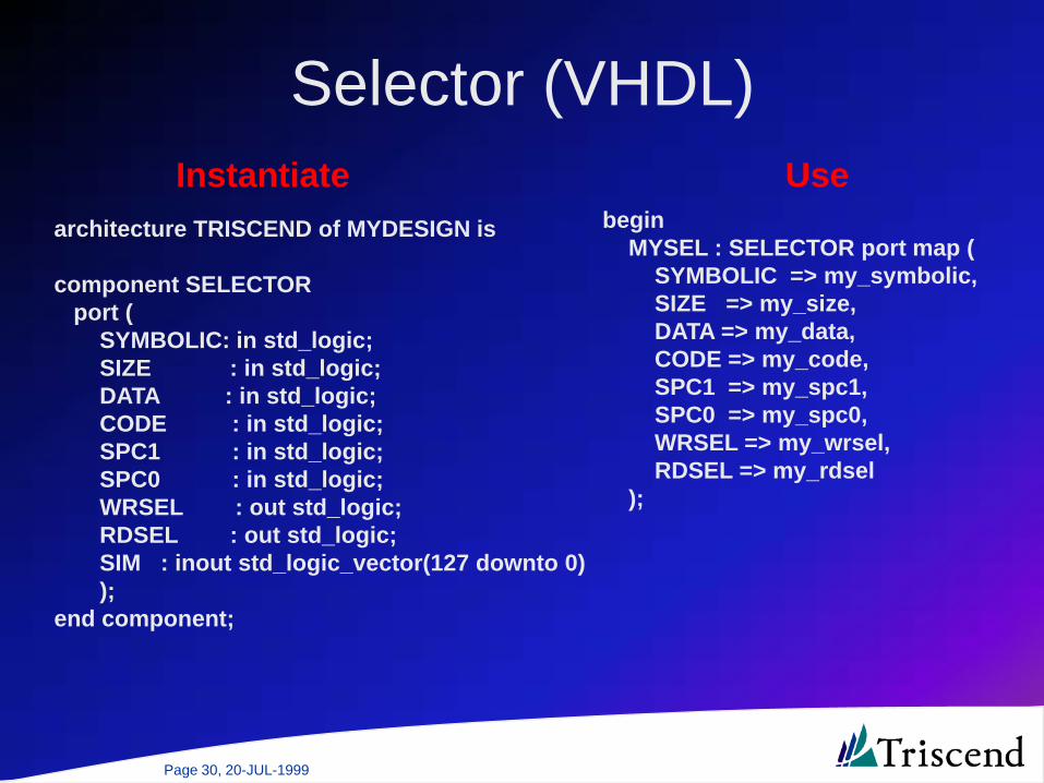
Selector (VHDL)
architecture TRISCEND of MYDESIGN is
component SELECTORport (
SYMBOLIC: in std_logic;SIZE : in std_logic;DATA : in std_logic;CODE : in std_logic;SPC1 : in std_logic;SPC0 : in std_logic;WRSEL : out std_logic;RDSEL : out std_logic; SIM : inout std_logic_vector(127 downto 0));
end component;
beginMYSEL : SELECTOR port map (
SYMBOLIC => my_symbolic,SIZE => my_size,DATA => my_data,CODE => my_code,SPC1 => my_spc1,SPC0 => my_spc0,WRSEL => my_wrsel,RDSEL => my_rdsel
);
Instantiate Use
Page 31, 20-JUL-1999
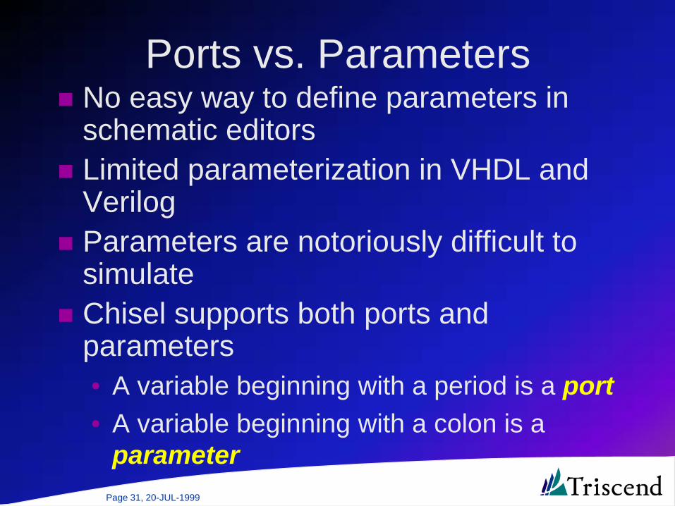
Ports vs. ParametersNo easy way to define parameters in schematic editorsLimited parameterization in VHDL and VerilogParameters are notoriously difficult to simulateChisel supports both ports and parameters• A variable beginning with a period is a port• A variable beginning with a colon is a
parameter
Page 32, 20-JUL-1999
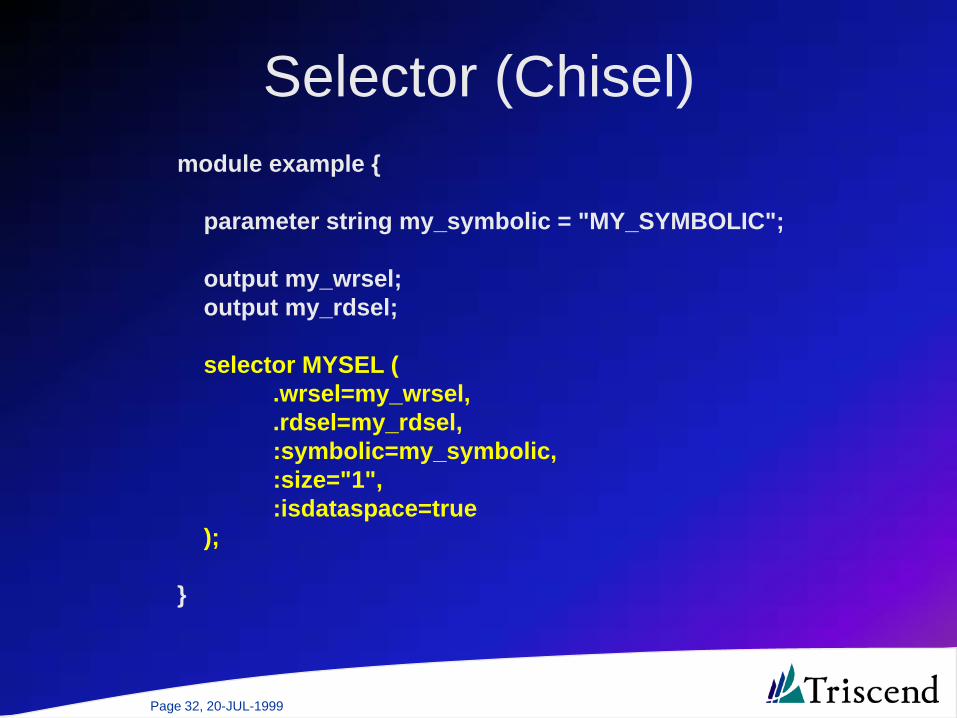
Selector (Chisel)module example {
parameter string my_symbolic = "MY_SYMBOLIC";
output my_wrsel;output my_rdsel;
selector MYSEL (.wrsel=my_wrsel,.rdsel=my_rdsel,:symbolic=my_symbolic,:size="1",:isdataspace=true
);
}
Page 33, 20-JUL-1999
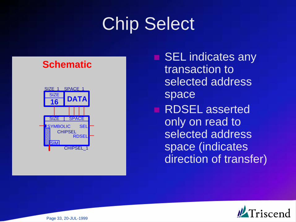
Chip Select
SEL indicates any transaction to selected address spaceRDSEL asserted only on read to selected address space (indicates direction of transfer)
Schematic
DATASPACE_1
SIZE SPACE
SIM
SYMBOLIC SEL
RDSEL
CHIPSEL_1
CHIPSEL
SIZE
16
SIZE_1

Page 34, 20-JUL-1999
Chip Select (Hardware)
Match0
Match1
A31
A0A1A2
CSI Bus Address
READ
BCLK
RDSEL
SELWRITE
Page 35, 20-JUL-1999
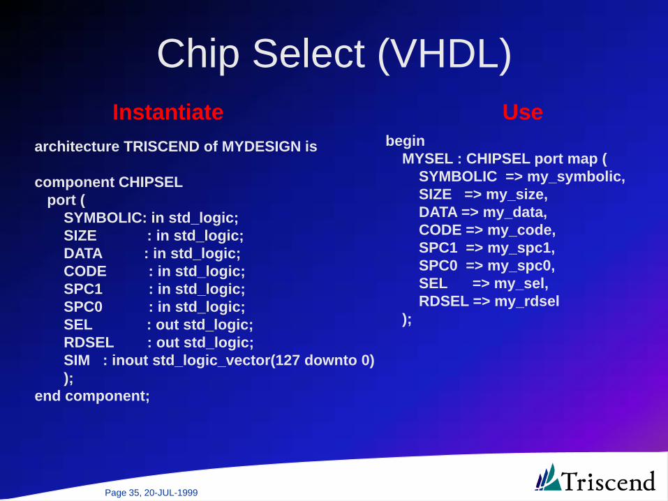
Chip Select (VHDL)
architecture TRISCEND of MYDESIGN is
component CHIPSELport (
SYMBOLIC: in std_logic;SIZE : in std_logic;DATA : in std_logic;CODE : in std_logic;SPC1 : in std_logic;SPC0 : in std_logic;SEL : out std_logic;RDSEL : out std_logic; SIM : inout std_logic_vector(127 downto 0));
end component;
beginMYSEL : CHIPSEL port map (
SYMBOLIC => my_symbolic,SIZE => my_size,DATA => my_data,CODE => my_code,SPC1 => my_spc1,SPC0 => my_spc0,SEL => my_sel,RDSEL => my_rdsel
);
Instantiate Use

Page 36, 20-JUL-1999
Chip Select (Chisel)
module example {
parameter string my_symbolic = "MY_SYMBOLIC";
output my_sel;output my_rdsel;
chipsel MYSEL (.sel=my_sel,.rdsel=my_rdsel,:symbolic=my_symbolic,:size="16",:isdataspace=true
);
}

Page 37, 20-JUL-1999
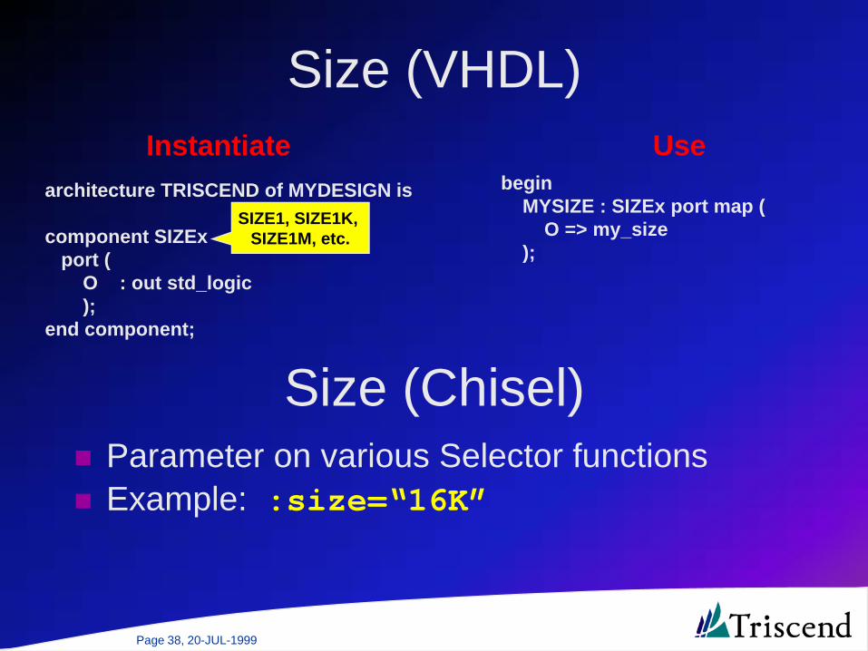
Defining the SIZEDefines number of bytes selected• Defines number of
“don’t care” bits for low-order address lines
Always a power of 2• SIZE1 = single byte• SIZE1K = 1 Kbyte• SIZE1M = 1 Mbyte
Up to 16M in E5 family
SIZE
1
SIZE_3SIZE
2
SIZE_4SIZE
4
SIZE_5SIZE
8
SIZE_6SIZE
16
SIZE_7
SIZE
32
SIZE_8SIZE
64
SIZE_9SIZE
128
SIZE_10SIZE
256
SIZE_11SIZE
512
SIZE_12
SIZE
1K
SIZE_13SIZE
2K
SIZE_14SIZE
4K
SIZE_15SIZE
8K
SIZE_16SIZE
16K
SIZE_17
SIZE
32K
SIZE_18SIZE
64K
SIZE_19SIZE
128K
SIZE_20SIZE
256K
SIZE_21SIZE
512K
SIZE_22
SIZE
1M
SIZE_23SIZE
2M
SIZE_24SIZE
4M
SIZE_25SIZE
8M
SIZE_26SIZE
16M
SIZE_27
Schematic
Page 38, 20-JUL-1999
architecture TRISCEND of MYDESIGN is
component SIZExport (
O : out std_logic);
end component;
Size (VHDL)
beginMYSIZE : SIZEx port map (
O => my_size);
Instantiate Use
Size (Chisel)
SIZE1, SIZE1K, SIZE1M, etc.
Parameter on various Selector functionsExample: :size=“16K”
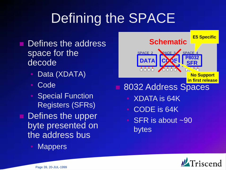
Page 39, 20-JUL-1999
Defining the SPACE
Defines the address space for the decode• Data (XDATA)• Code• Special Function
Registers (SFRs)Defines the upper byte presented on the address bus• Mappers
DATASPACE_2
CODESPACE_3
SFRP8032
SPACE_4
8032 Address Spaces• XDATA is 64K• CODE is 64K• SFR is about ~90
bytes
SchematicE5 Specific
No Supportin first release
Page 40, 20-JUL-1999
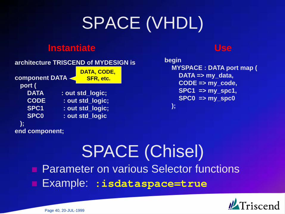
SPACE (VHDL)
architecture TRISCEND of MYDESIGN is
component DATAport (
DATA : out std_logic;CODE : out std_logic;SPC1 : out std_logic;SPC0 : out std_logic
);end component;
beginMYSPACE : DATA port map (
DATA => my_data,CODE => my_code,SPC1 => my_spc1,SPC0 => my_spc0
);
Instantiate Use
DATA, CODE, SFR, etc.
Parameter on various Selector functionsExample: :isdataspace=true
SPACE (Chisel)

Page 41, 20-JUL-1999
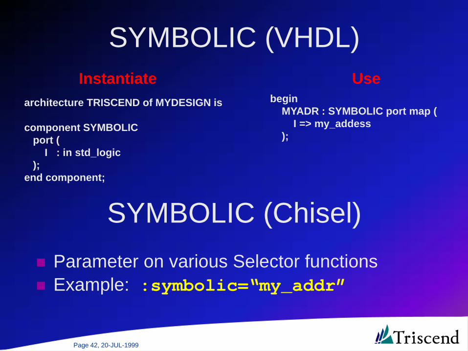
SYMBOLIC
Defines a net as a symbolic nameSymbolic inputs are treated separately from normal input netsMaintains simulation capability (no parameters)
Schematic
SYMBOLIC
SYMBOLIC_1
Page 42, 20-JUL-1999
SYMBOLIC (VHDL)
architecture TRISCEND of MYDESIGN is
component SYMBOLICport (
I : in std_logic);
end component;
beginMYADR : SYMBOLIC port map (
I => my_addess);
Instantiate Use
SYMBOLIC (Chisel)Parameter on various Selector functionsExample: :symbolic=“my_addr”
Page 43, 20-JUL-1999
Example: Read/Write Register
SIM[127..0]
DR4
DW1
BUSCLK
DW2DW3
DR7DW6DW7
CPU_RESET
DR5DW5
WRSEL
DR0
DW4
RDSEL
DR1
DR6
DR2
DW0
DR3
D
EN
Q
CLRDFF_6
DFF
BU
S
SIM
DR0
DR1
DR2
DR3
DR4
DR5
DR6
DR7
EN
DR7_0E_1DR7_0E
SIM
BUSCLK_1
BUSCLK
D
EN
Q
CLRDFF_1
DFF
SIZE SPACE
SIM
SYMBOLIC WRSEL
RDSEL
SELECTOR_1
SELECTOR
DATASPACE_1
BU
S
SIMDW0
DW1
DW2
DW3
DW4
DW5
DW6
DW7
DW7_0_1DW7_0
D
EN
Q
CLRDFF_7
DFF
D
EN
Q
CLRDFF_4
DFF
D
EN
Q
CLRDFF_5
DFF
D
EN
Q
CLRDFF_8
DFF
D
EN
Q
CLRDFF_3
DFF
SIZE
1
SIZE_1
D
EN
Q
CLRDFF_2
DFF
SYMBOLICSYMBOLIC_1
SIM
CPUWAS RESET
CPURST_1
CPURST
MyAddress
Page 44, 20-JUL-1999
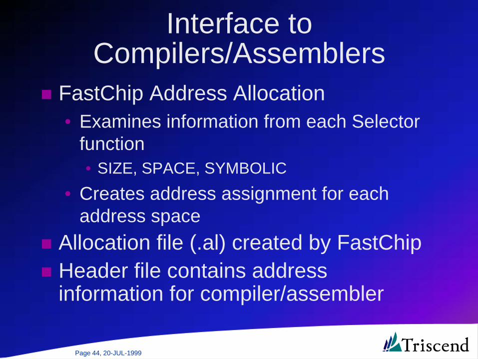
Interface to Compilers/Assemblers
FastChip Address Allocation• Examines information from each Selector
function• SIZE, SPACE, SYMBOLIC
• Creates address assignment for each address space
Allocation file (.al) created by FastChipHeader file contains address information for compiler/assembler

Page 45, 20-JUL-1999
Example Allocation File
// Allocation written 7/10/99 5:27 AM// By FastChip Version Preview 4 Release 061999 Build 08// Summary of zones:// -----------------// CRU_DATA (DMAP3) L:0xff00:0xffff P:0x2_0e00:0x2_0eff F:0 T:0x98 A:0x0// USER_DATA_C (DMAP2) L:0x0000:0x1fff P:0x1_8000:0x1_9fff F:0 T:0x90 A:0x0// USER_DATA_D (DMAP1) L:0x0000:0xffff P:0x10_0000:0x10_ffff F:1 T:0x88 A:0x0// SRAM_DATA (DMAP0) L:0x0000:0xffff P:0x2_0000:0x2_ffff F:0 T:0x80 A:0x0// USER_CODE_B (CMAP1) L:0x0000:0x7fff P:0x1_0000:0x1_7fff F:0 T:0x28 A:0x48// ROM_CODE (CMAP0) L:0x0000:0x03ff P:0x0000:0x03ff F:0 T:0x20 A:0x40// SFR_DATA (XMAP) L:0x0080:0x00ff P:0x1f_ff80:0x1f_ffff F:1 T:0xc0 A:0xe0S E520JTAG;A "Result.CMDREG" "Result" "USER_DATA_D" 0x2000; // 0x10_2000A "Switch.STATREG" "Switch" "SFR_DATA" 0x009a; // 0x1f_ff9a
Located in ‘data/ProjectRegistry/<proj>’File is named ‘<proj>.al’
Mapperprogramminginformation
Allocationstyle
Assigned user locations
Page 46, 20-JUL-1999
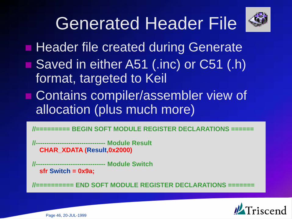
Generated Header FileHeader file created during GenerateSaved in either A51 (.inc) or C51 (.h) format, targeted to KeilContains compiler/assembler view of allocation (plus much more)
//========= BEGIN SOFT MODULE REGISTER DECLARATIONS ======
//-------------------------------- Module Result CHAR_XDATA (Result,0x2000)
//-------------------------------- Module Switch sfr Switch = 0x9a;
//========== END SOFT MODULE REGISTER DECLARATIONS =======
Page 47, 20-JUL-1999
Converting an Existing8032 Design to CSI Bus

Page 48, 20-JUL-1999
Data InterfaceREAD
AD0 WWD0
RRD0
AD1 WWD1RRD1
AD2 WWD2RRD2
AD3 WWD3
RRD3
AD4 WWD4
RRD4
AD5 WWD5RRD5
AD6 WWD6RRD6
AD7 WWD7
RRD7
U11
IBUF
U12
IBUF
U13
IBUF
U14
IBUF
U15
IBUF
U16
IBUF
U17
IBUF
U18
IBUF
TU20
OBUFT
TU21
OBUFT
TU22
OBUFT
TU23
OBUFT
TU24
OBUFT
TU25
OBUFT
TU26
OBUFT
TU27
OBUFT
XR1PULLUP
XR2PULLUP
XR3PULLUP
XR4PULLUP
XR5PULLUP
XR6PULLUP
XR7PULLUP
XR8PULLUP
U197
IOPADLOC=P77
U198
IOPADLOC=P78
U199
IOPADLOC=P79
U200
IOPADLOC=P80
U201
IOPADLOC=P81
U202
IOPADLOC=P82
U203
IOPADLOC=P83
U204
IOPADLOC=P84
8032 data interface embedded on CSI busSaves I/O pin countReduces power consumption and EMIReplaced by CSI Bus Data Write and Data Read primitives
Original Design
Page 49, 20-JUL-1999
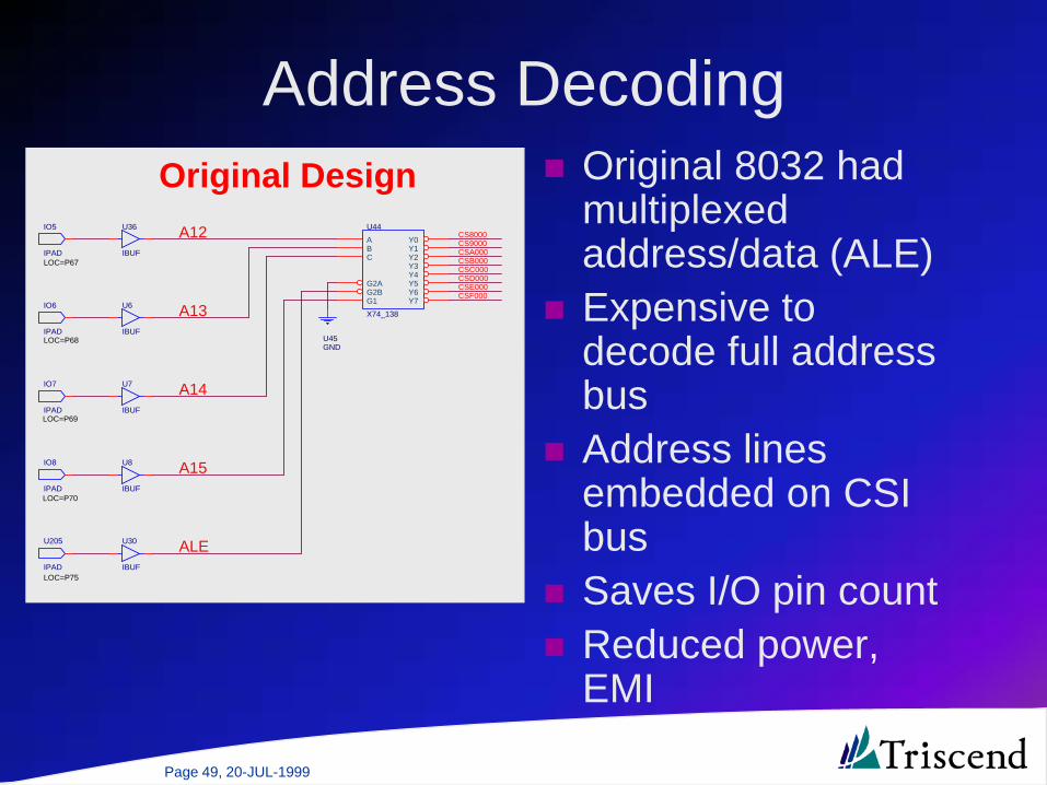
Address DecodingOriginal 8032 had multiplexed address/data (ALE)Expensive to decode full address busAddress lines embedded on CSI busSaves I/O pin countReduced power, EMI
A12 CS8000CS9000CSA000CSB000CSC000CSD000CSE000CSF000
A13
A14
A15
ALE
U6
IBUF
U7
IBUF
U8
IBUF
U30
IBUF
U36
IBUF
U44
X74_138
ABC
G2AG2BG1
Y0Y1Y2Y3Y4Y5Y6Y7
U45GND
IO5
IPADLOC=P67
IO6
IPADLOC=P68
IO7
IPADLOC=P69
IO8
IPADLOC=P70
U205
IPADLOC=P75
Original Design

Page 50, 20-JUL-1999
Addressing RegistersCSI bus Selectors replace address decoding logic in the applicationSee Read/Write ExampleCSI approach is safe, synchronous design
Original Design
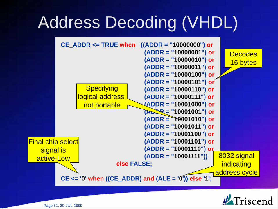
Page 51, 20-JUL-1999
Address Decoding (VHDL)CE_ADDR <= TRUE when ((ADDR = "10000000") or
(ADDR = "10000001") or(ADDR = "10000010") or(ADDR = "10000011") or(ADDR = "10000100") or(ADDR = "10000101") or(ADDR = "10000110") or(ADDR = "10000111") or(ADDR = "10001000") or(ADDR = "10001001") or(ADDR = "10001010") or(ADDR = "10001011") or(ADDR = "10001100") or(ADDR = "10001101") or(ADDR = "10001110") or(ADDR = "10001111"))
else FALSE;
CE <= '0' when ((CE_ADDR) and (ALE = '0')) else '1';
Decodes16 bytes
8032 signalindicating
address cycle
Final chip selectsignal is
active-Low
Specifyinglogical address,
not portable
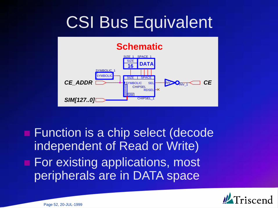
Page 52, 20-JUL-1999
CSI Bus Equivalent
SIZE SPACE
SIM
SYMBOLIC SEL
RDSEL
CHIPSEL_1
CHIPSEL
SIZE
16
SIZE_1
DATASPACE_1
INV_1INV
SYMBOLIC
SYMBOLIC_1
CECE_ADDR
SIM[127..0]
Schematic
Function is a chip select (decode independent of Read or Write)For existing applications, most peripherals are in DATA space
Page 53, 20-JUL-1999
Creating Address Structures
Relative Assignments and Offsets
Page 54, 20-JUL-1999
Creating Memory Structures
Symbolic addressing allows technology-independent designHow do you create a memory structure?• Very important for DMA operations• DMA requires contiguous addresses
Need ability to specify relationships• Parent-child relationships• Offset between addresses

Page 55, 20-JUL-1999
Relative Addressing Example
SIZE SPACE
SIM
SYMBOLIC WRSEL
RDSEL
SELECTOR_1
SELECTOR
SIZE
16
SIZE_28
DATASPACE_5
SIZE SPACE
SIM
SYMBOLIC WRSEL
RDSEL
SELECTOR_2
SELECTOR
DATASPACE_6
SIZE
1
SIZE_30OFFSET
PARENT
CHILD
OFFSET_1OFFSET
SIZE
16
SIZE_29
SYMBOLICSYMBOLIC_2
SYMBOLICSYMBOLIC_3
SIZE16_WRSYM_SIZE16
SYM_SIZE1
SIZE16_RD
SIZE1_WRSIZE1_RD
SIM[127..0]
Parent
Child
Offset
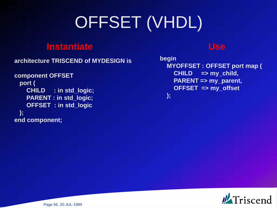
Page 56, 20-JUL-1999
OFFSET (VHDL)
architecture TRISCEND of MYDESIGN is
component OFFSETport (
CHILD : in std_logic;PARENT : in std_logic;OFFSET : in std_logic
);end component;
beginMYOFFSET : OFFSET port map (
CHILD => my_child,PARENT => my_parent,OFFSET => my_offset
);
Instantiate Use

Page 57, 20-JUL-1999
OFFSET (Chisel)selector MYSIZE16 (
.wrsel=size16_wr,
.rdsel=size16_rd,:symbolic="SYM_SIZE16",:size="16",:isdataspace=true
);
selector MYSIZE1 (.wrsel=size1_wr,.rdsel=size1_rd,:symbolic="SYM_SIZE1",:size="1",:isdataspace=true,:relative="SYM_SIZE16",:offset=16
);
Parent
Child
Offset
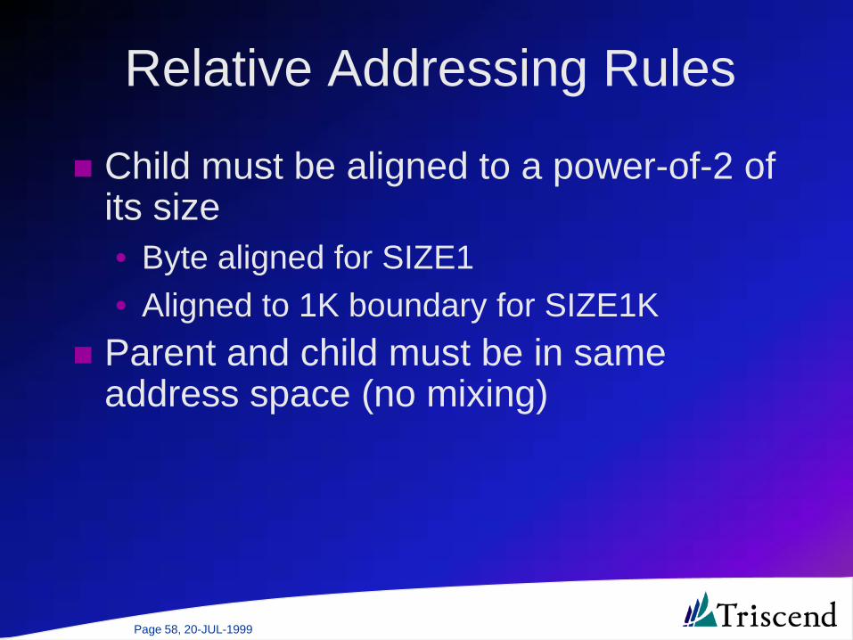
Page 58, 20-JUL-1999
Relative Addressing Rules
Child must be aligned to a power-of-2 of its size• Byte aligned for SIZE1• Aligned to 1K boundary for SIZE1K
Parent and child must be in same address space (no mixing)

Page 59, 20-JUL-1999
DMA Operations
Page 60, 20-JUL-1999
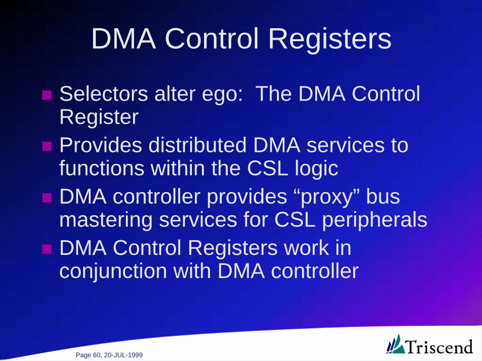
DMA Control Registers
Selectors alter ego: The DMA Control RegisterProvides distributed DMA services to functions within the CSL logicDMA controller provides “proxy” bus mastering services for CSL peripheralsDMA Control Registers work in conjunction with DMA controller

Page 61, 20-JUL-1999
DMA Control Register
Provides Request and Acknowledge steering to selected DMA channelAlways one byteExists in either Data or SFR spaceControl register located at SYMBOLIC address
Schematic
SPACE
SIM
SYMBOLIC
ACKSELREQSEL
DMACTRL_1
DMACTRL
DATASPACE_5
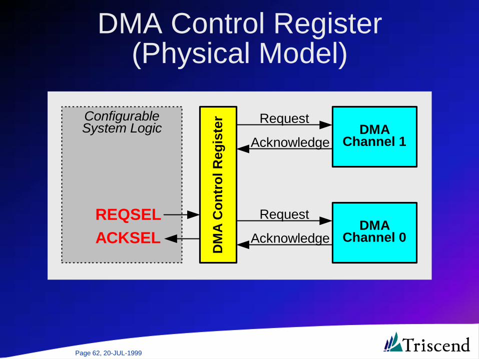
Page 62, 20-JUL-1999
DMA Control Register (Physical Model)
REQSEL
ConfigurableSystem Logic
DM
A C
ontr
ol R
egis
ter
ACKSEL
DMAChannel 1
Request
Acknowledge
DMAChannel 0
Request
Acknowledge
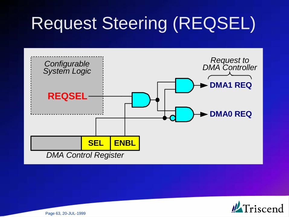
Page 63, 20-JUL-1999
Request Steering (REQSEL)
REQSEL
ENBLSEL
ConfigurableSystem Logic
DMA Control Register
DMA0 REQ
Request toDMA Controller
DMA1 REQ
Page 64, 20-JUL-1999
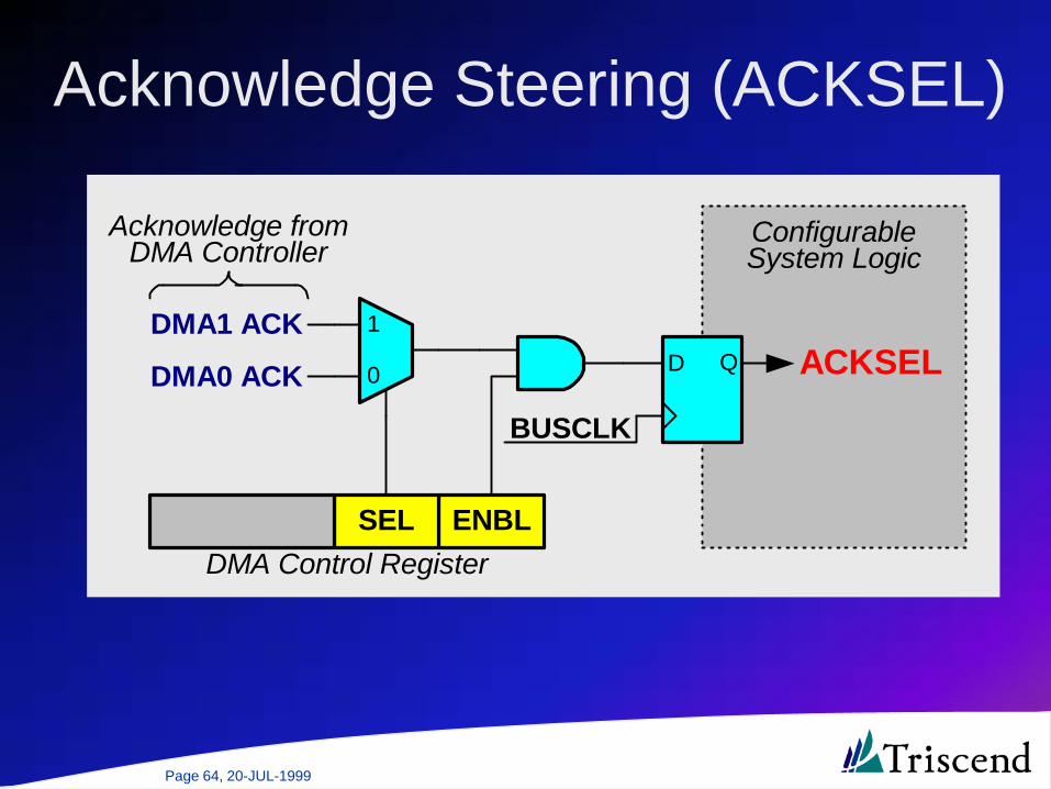
Acknowledge Steering (ACKSEL)
BUSCLK
D Q ACKSEL
ENBLSEL
1
0
ConfigurableSystem Logic
DMA Control Register
DMA1 ACK
DMA0 ACK
Acknowledge fromDMA Controller
Page 65, 20-JUL-1999
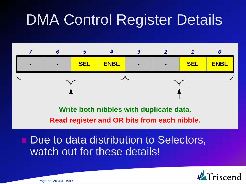
DMA Control Register Details
- - SEL ENBL - - SEL ENBL
7 6 5 4 3 2 1 0
Write both nibbles with duplicate data.Read register and OR bits from each nibble.
Due to data distribution to Selectors, watch out for these details!
Page 66, 20-JUL-1999
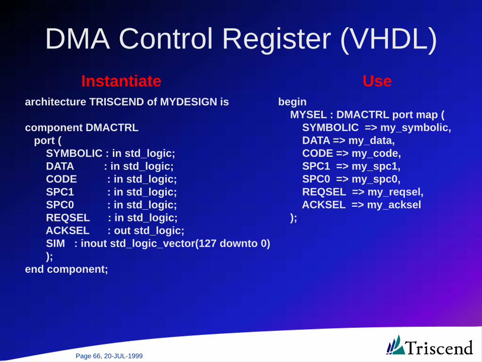
DMA Control Register (VHDL)
architecture TRISCEND of MYDESIGN is
component DMACTRLport (
SYMBOLIC : in std_logic;DATA : in std_logic;CODE : in std_logic;SPC1 : in std_logic;SPC0 : in std_logic;REQSEL : in std_logic;ACKSEL : out std_logic; SIM : inout std_logic_vector(127 downto 0));
end component;
beginMYSEL : DMACTRL port map (
SYMBOLIC => my_symbolic,DATA => my_data,CODE => my_code,SPC1 => my_spc1,SPC0 => my_spc0,REQSEL => my_reqsel,ACKSEL => my_acksel
);
Instantiate Use

Page 67, 20-JUL-1999
DMA Control Register (Chisel)module example {
parameter string my_symbolic = "MY_SYMBOLIC";
input my_reqsel;output my_acksel;
dmactrl MYSEL (.reqsel=my_reqsel,.acksel=my_acksel,:symbolic=my_symbolic,:isdataspace=true,:enabled=false,:channel=0
);
}
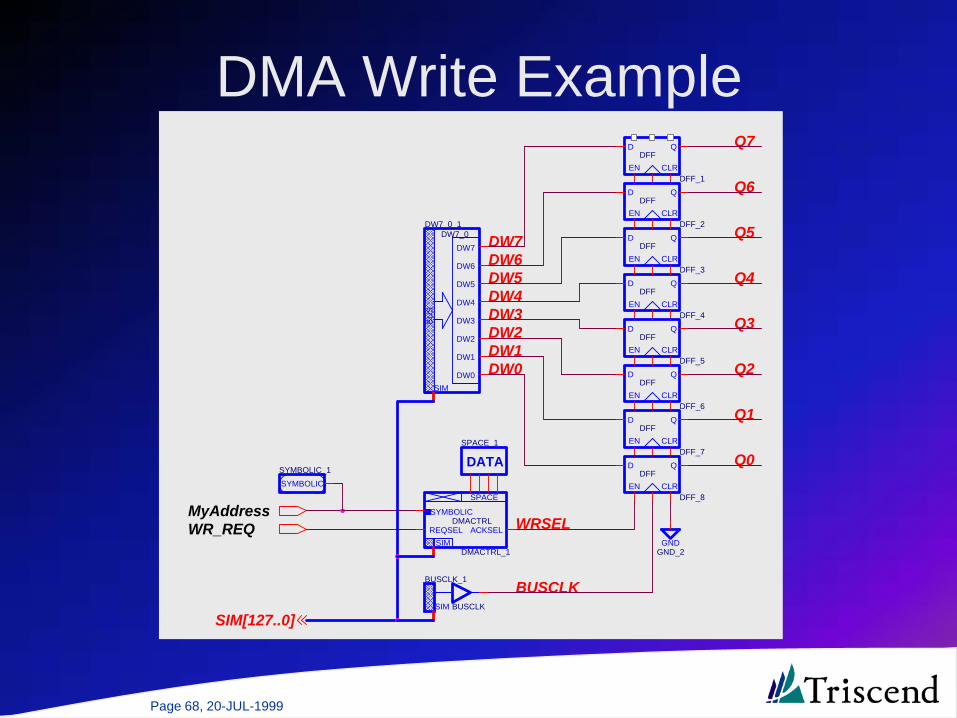
Page 68, 20-JUL-1999
DMA Write Example
SIM[127..0]
DW1DW2DW3
Q2
Q5
DW6DW7
Q6
DW5
WRSEL
Q7
DW4
Q0
DW0
Q1
Q3
Q4
BUSCLK
D
EN
Q
CLRDFF_6
DFF
SIM
BUSCLK_1
BUSCLK
D
EN
Q
CLRDFF_1
DFF
DATASPACE_1
BU
S
SIMDW0
DW1
DW2
DW3
DW4
DW5
DW6
DW7
DW7_0_1DW7_0
D
EN
Q
CLRDFF_7
DFF
D
EN
Q
CLRDFF_4
DFF
D
EN
Q
CLRDFF_5
DFF
D
EN
Q
CLRDFF_8
DFF
D
EN
Q
CLRDFF_3
DFF
D
EN
Q
CLRDFF_2
DFF
SYMBOLIC
SYMBOLIC_1
SPACE
SIM
SYMBOLIC
ACKSELREQSEL
DMACTRL_1
DMACTRL
GNDGND_2
MyAddressWR_REQ
Page 69, 20-JUL-1999
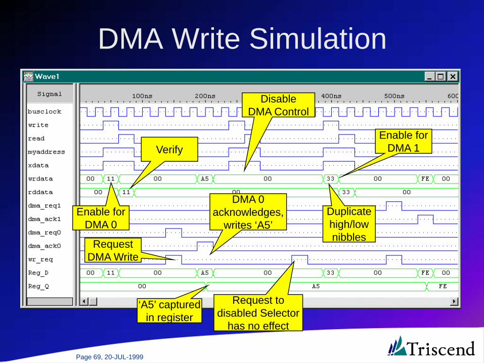
DMA Write Simulation
Enable forDMA 0
Verify
RequestDMA Write
DMA 0acknowledges,
writes ‘A5’
‘A5’ capturedin register
DisableDMA Control
Request todisabled Selector
has no effect
Enable forDMA 1
Duplicatehigh/lownibbles
Page 70, 20-JUL-1999
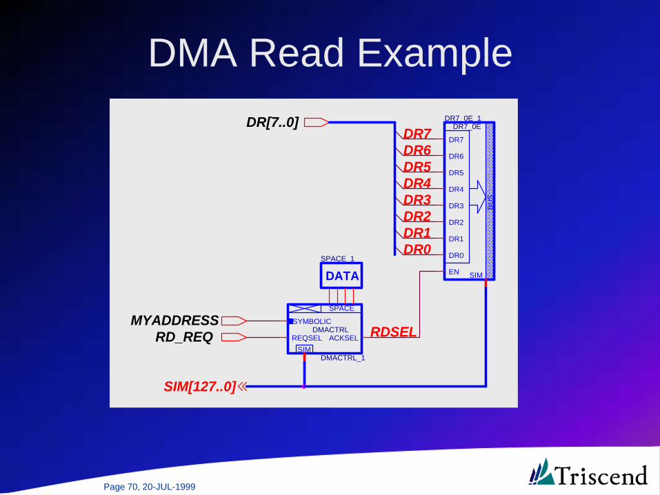
DMA Read Example
SIM[127..0]
DR7DR6DR5DR4DR3DR2DR1DR0
RDSEL
BU
S
SIM
DR0
DR1
DR2
DR3
DR4
DR5
DR6
DR7
EN
DR7_0E_1DR7_0E
DATASPACE_1
SPACE
SIM
SYMBOLIC
ACKSELREQSEL
DMACTRL_1
DMACTRLMYADDRESS
RD_REQ
DR[7..0]

Page 71, 20-JUL-1999
DMA Read Simulation
Enable forDMA 0
Verify
RequestDMA Read
DMA 0acknowledges,
reads ‘A5’
‘A5’ appearson Data Read

Page 72, 20-JUL-1999
CSI SIM Bus Models
Page 73, 20-JUL-1999
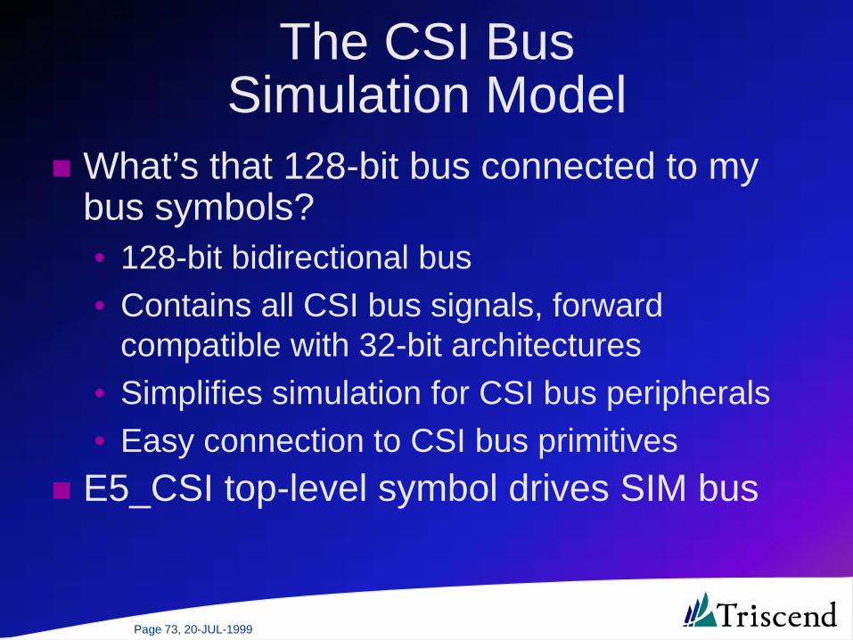
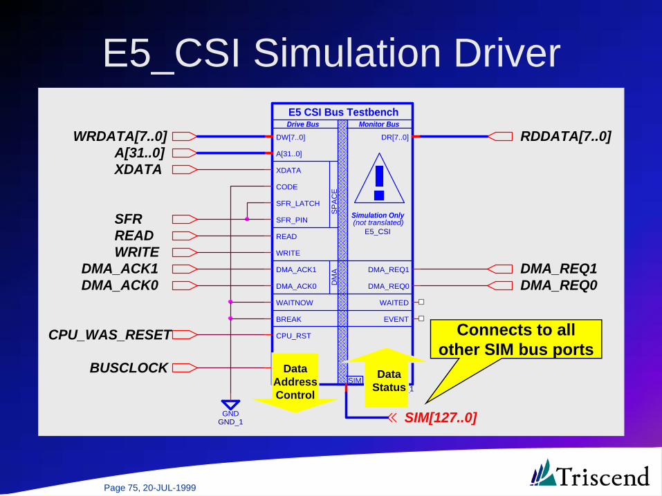
The CSI BusSimulation Model
What’s that 128-bit bus connected to my bus symbols?• 128-bit bidirectional bus• Contains all CSI bus signals, forward
compatible with 32-bit architectures• Simplifies simulation for CSI bus peripherals• Easy connection to CSI bus primitives
E5_CSI top-level symbol drives SIM bus
Page 74, 20-JUL-1999
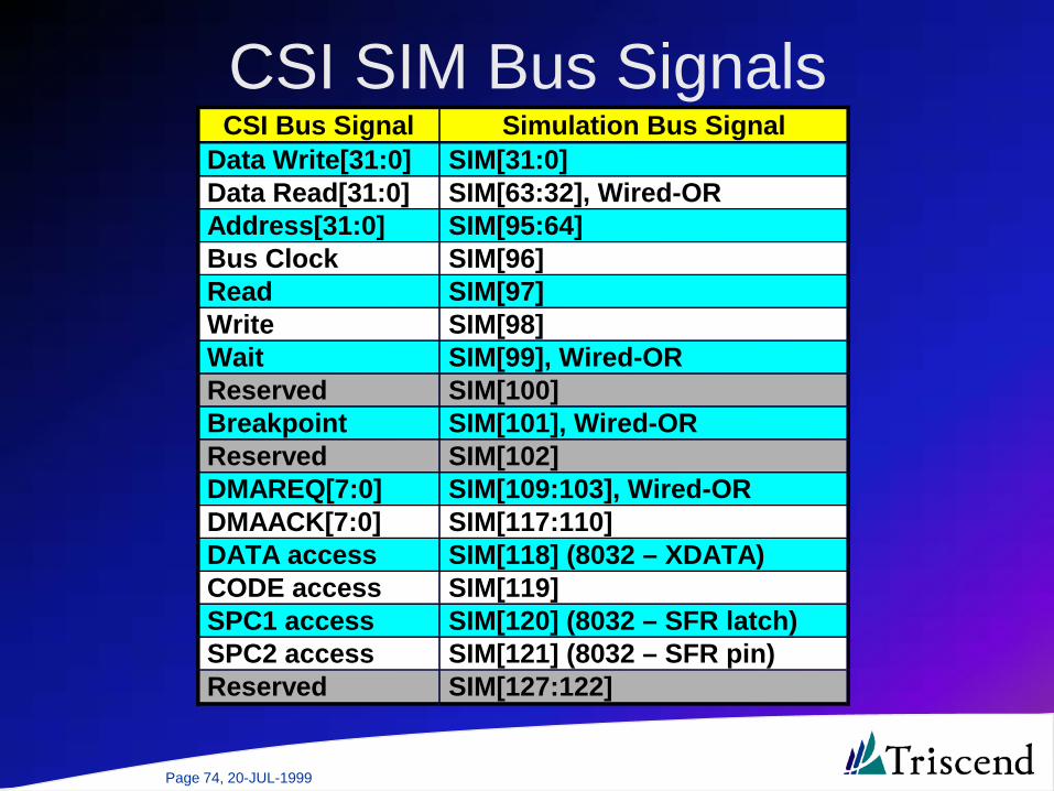
CSI SIM Bus SignalsCSI Bus Signal Simulation Bus Signal
Data Write[31:0] SIM[31:0]Data Read[31:0] SIM[63:32], Wired-ORAddress[31:0] SIM[95:64]Bus Clock SIM[96]Read SIM[97]Write SIM[98]Wait SIM[99], Wired-ORReserved SIM[100]Breakpoint SIM[101], Wired-ORReserved SIM[102]DMAREQ[7:0] SIM[109:103], Wired-ORDMAACK[7:0] SIM[117:110]DATA access SIM[118] (8032 – XDATA)CODE access SIM[119]SPC1 access SIM[120] (8032 – SFR latch)SPC2 access SIM[121] (8032 – SFR pin)Reserved SIM[127:122]
Page 75, 20-JUL-1999
E5_CSI Simulation Driver
SIM[127..0]
DW[7..0]
A[31..0]
XDATA
CODE
SFR_LATCH
SFR_PIN
READ
WRITE
DMA_ACK1
DMA_ACK0
WAITNOW
BREAK EVENT
WAITED
DMA_REQ0
DMA_REQ1
DR[7..0]
SP
AC
ED
MA
E5 CSI Bus TestbenchDrive Bus Monitor Bus
Simulation Only(not translated)
SIM
CPU_RST
E5_CSI_1
E5_CSI
GNDGND_1
WRDATA[7..0]A[31..0]XDATA
SFRREADWRITE
BUSCLOCK
CPU_WAS_RESET
RDDATA[7..0]
DMA_REQ1DMA_REQ0
DMA_ACK1DMA_ACK0
Connects to allother SIM bus ports
DataAddressControl
DataStatus

Page 76, 20-JUL-1999
Example: Read/Write Register
SIM[127..0]
DR4
DW1
BUSCLK
DW2DW3
DR7DW6DW7
CPU_RESET
DR5DW5
WRSEL
DR0
DW4
RDSEL
DR1
DR6
DR2
DW0
DR3
D
EN
Q
CLRDFF_6
DFF
BU
S
SIM
DR0
DR1
DR2
DR3
DR4
DR5
DR6
DR7
EN
DR7_0E_1DR7_0E
SIM
BUSCLK_1
BUSCLK
D
EN
Q
CLRDFF_1
DFF
SIZE SPACE
SIM
SYMBOLIC WRSEL
RDSEL
SELECTOR_1
SELECTOR
DATASPACE_1
BU
S
SIMDW0
DW1
DW2
DW3
DW4
DW5
DW6
DW7
DW7_0_1DW7_0
D
EN
Q
CLRDFF_7
DFF
D
EN
Q
CLRDFF_4
DFF
D
EN
Q
CLRDFF_5
DFF
D
EN
Q
CLRDFF_8
DFF
D
EN
Q
CLRDFF_3
DFF
SIZE
1
SIZE_1
D
EN
Q
CLRDFF_2
DFF
SYMBOLICSYMBOLIC_1
SIM
CPUWAS RESET
CPURST_1
CPURST
MyAddress
Page 77, 20-JUL-1999
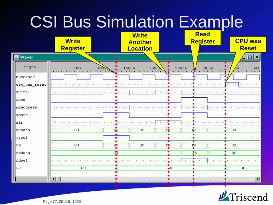
CSI Bus Simulation ExampleWrite
Register
WriteAnotherLocation
CPU wasReset
ReadRegister
Page 78, 20-JUL-1999
Wait-State and Breakpoint
Page 79, 20-JUL-1999
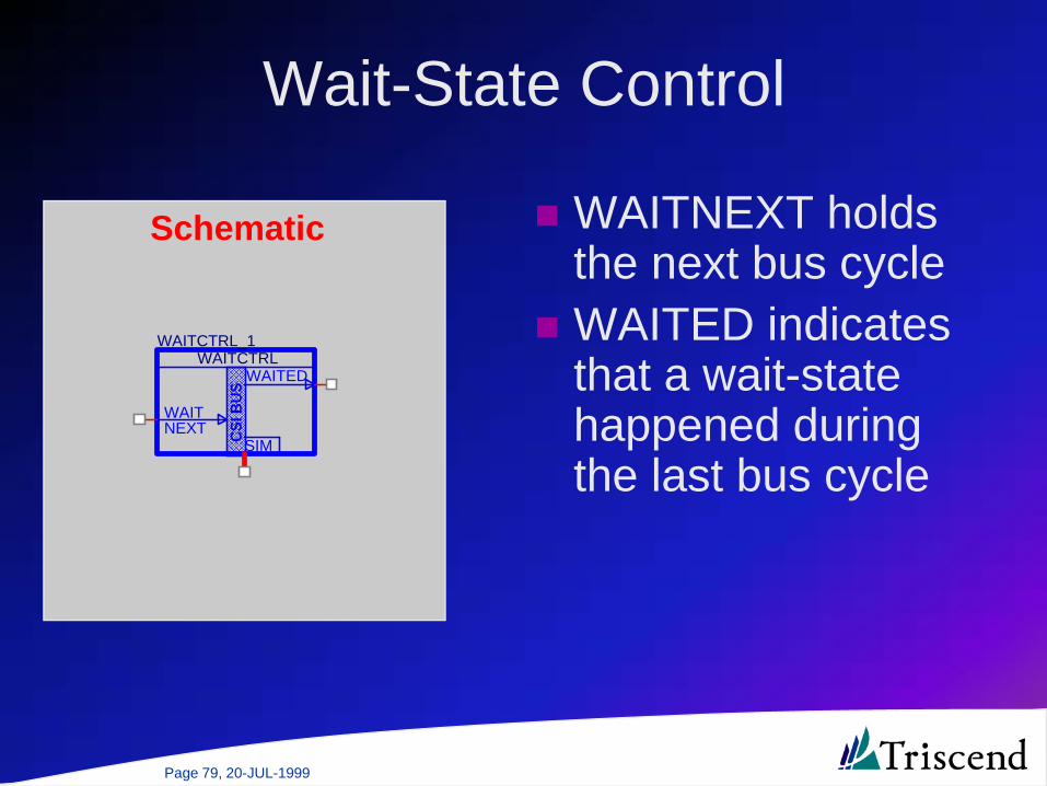
Wait-State Control
Schematic WAITNEXT holds the next bus cycleWAITED indicates that a wait-state happened during the last bus cycle
WAITED
WAIT
SIMNEXT CS
I BUS
WAITCTRL_1WAITCTRL
Page 80, 20-JUL-1999
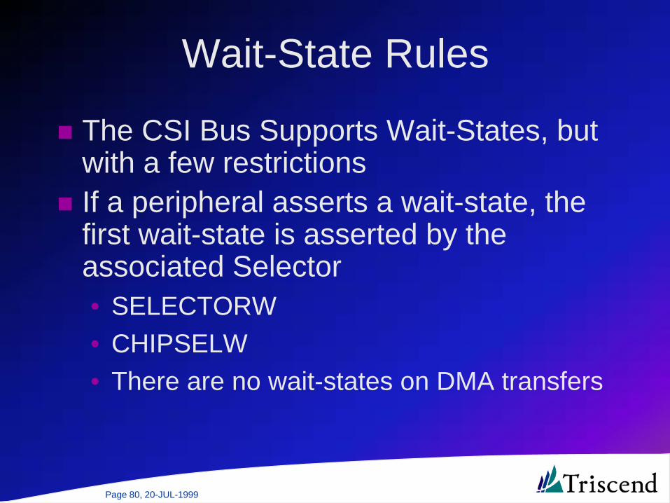
Wait-State Rules
The CSI Bus Supports Wait-States, but with a few restrictionsIf a peripheral asserts a wait-state, the first wait-state is asserted by the associated Selector• SELECTORW• CHIPSELW• There are no wait-states on DMA transfers
Page 81, 20-JUL-1999
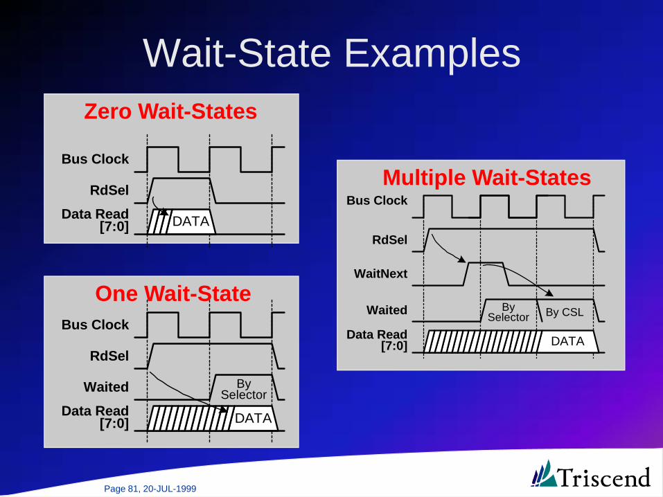
Wait-State Examples
Bus Clock
Waited BySelector
RdSel
DATAData Read[7:0]
One Wait-State
Bus Clock
RdSel
DATAData Read[7:0]
Zero Wait-States
Bus Clock
RdSel
Waited BySelector By CSL
WaitNext
DATAData Read[7:0]
Multiple Wait-States

Page 82, 20-JUL-1999
Wait-State Control (VHDL)
architecture TRISCEND of MYDESIGN is
component WAITCTRLport (
WAITNEXT : in std_logic;WAITED : out std_logic;SIM : inout std_logic_vector(127 downto 0));
end component;
beginMYWAIT : WAITCTRL port map (
WAITNEXT => my_waitnext,WAITED => my_waited
);
Instantiate Use
Page 83, 20-JUL-1999
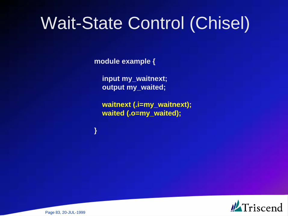
Wait-State Control (Chisel)
module example {
input my_waitnext;output my_waited;
waitnext (.i=my_waitnext);waited (.o=my_waited);
}
Page 84, 20-JUL-1999
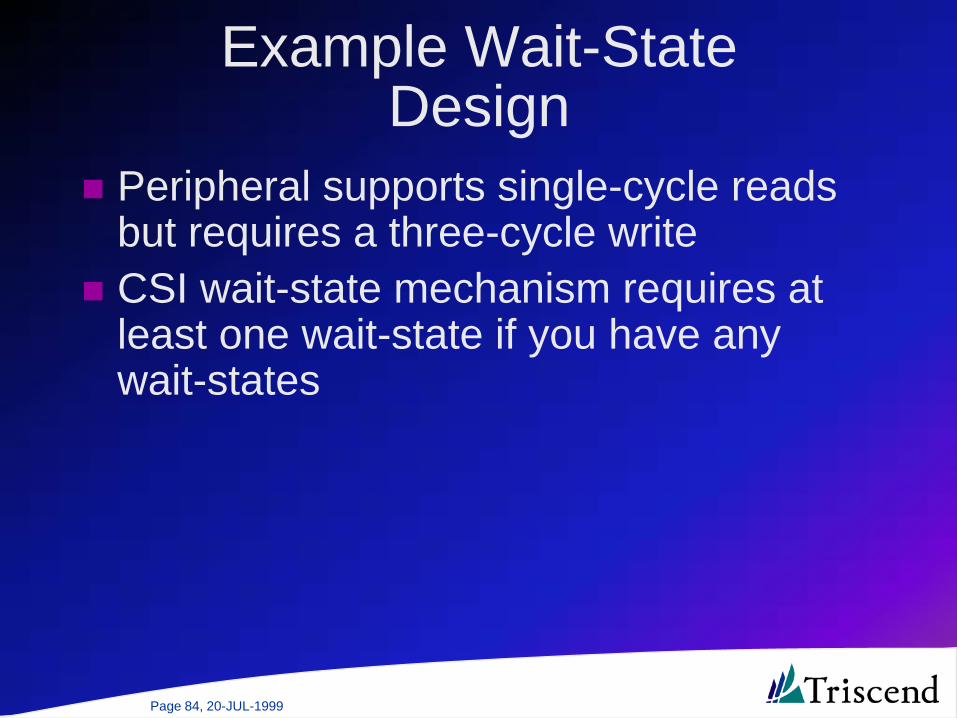
Example Wait-State Design
Peripheral supports single-cycle reads but requires a three-cycle writeCSI wait-state mechanism requires at least one wait-state if you have any wait-states
Page 85, 20-JUL-1999
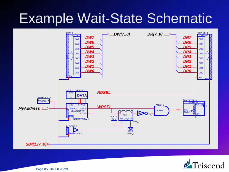
Example Wait-State Schematic
SIM[127..0]
DW7DW6DW5DW4DW3DW2DW1DW0
DR5
DR3
RDSEL
WRSEL
DR2
DR0DR1
NEXT
DR4
DR7DR6
DATASPACE_1
BU
S
SIMDW0
DW1
DW2
DW3
DW4
DW5
DW6
DW7
DW7_0_1DW7_0
SIZE
1
SIZE_1
SYMBOLIC
SYMBOLIC_1
SIM
BUSCLK_1
BUSCLK
SIZE SPACE
SIM
SYMBOLIC WRSEL
RDSEL
SELECTORW_1
SELECTORWINV_1INV
GNDGND_2
BU
S
SIM
DR0
DR1
DR2
DR3
DR4
DR5
DR6
DR7
EN
DR7_0E_1DR7_0E
D
EN
Q
CLRDFF_1
DFF
VCCVCC_1
WAITED
WAIT
SIMNEXT CS
I BUS
WAITCTRL_1WAITCTRL
AND2_1
AND2
DW[7..0]
MyAddress
DR[7..0]

Page 86, 20-JUL-1999
Example Wait-State Simulation
Wait-statefrom Selector
Wait signalon SIM bus
Wait-statefrom logic
WRSELextended
Waited fortwo cycles
Wait-statefrom Selector
Page 87, 20-JUL-1999
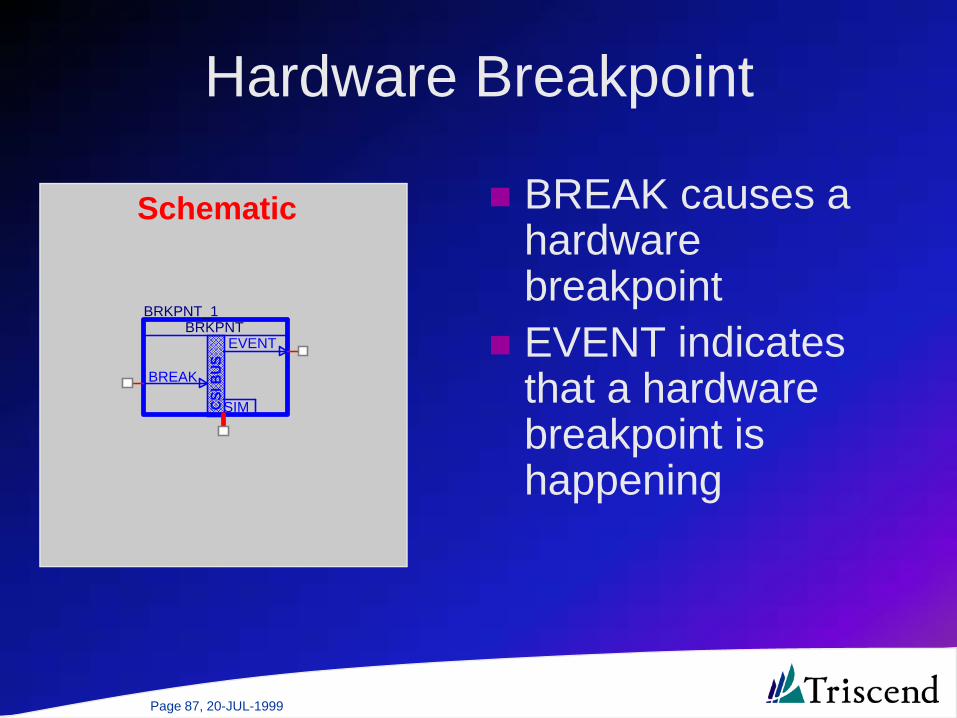
Hardware Breakpoint
Schematic BREAK causes a hardware breakpointEVENT indicates that a hardware breakpoint is happening
EVENT
BREAK
SIMCSI B
US
BRKPNT_1BRKPNT
Page 88, 20-JUL-1999
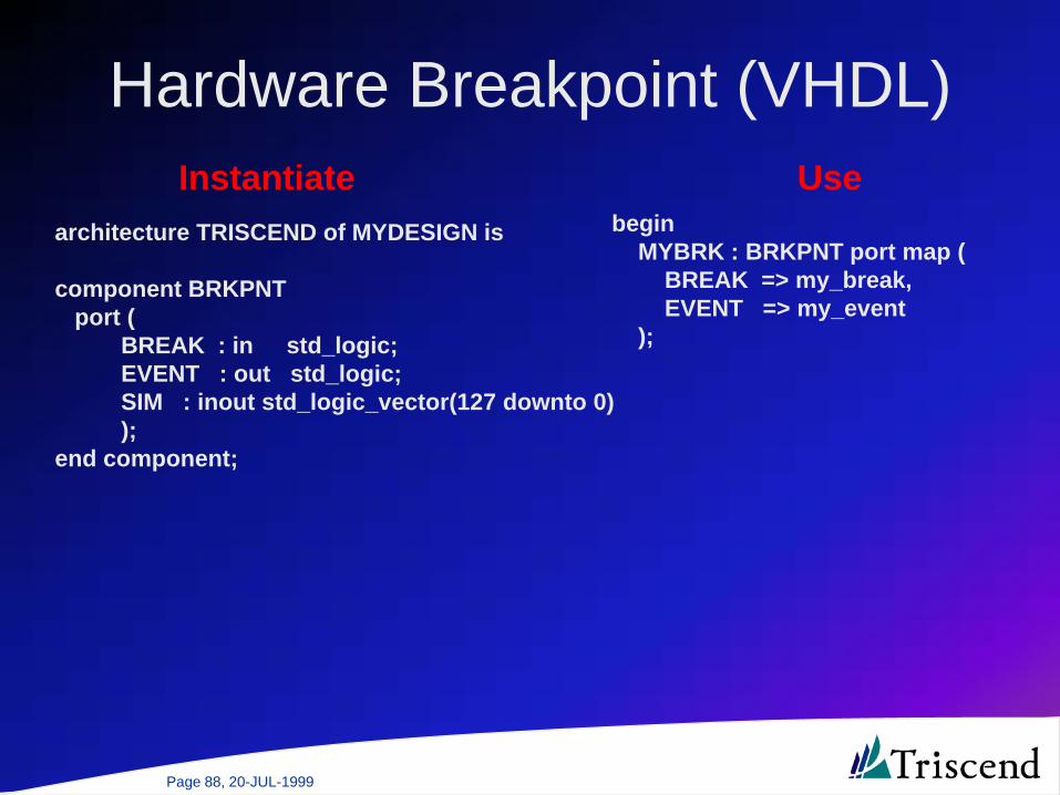
Hardware Breakpoint (VHDL)
architecture TRISCEND of MYDESIGN is
component BRKPNTport (
BREAK : in std_logic;EVENT : out std_logic;SIM : inout std_logic_vector(127 downto 0));
end component;
beginMYBRK : BRKPNT port map (
BREAK => my_break,EVENT => my_event
);
Instantiate Use

Page 89, 20-JUL-1999
Hardware Breakpoint (Chisel)
module example {
input my_break;output my_event;
bpctl BREAK (.i=my_break);bpevt EVENT (.o=my_event);
}

Page 90, 20-JUL-1999
Summary
The Configurable System Interconnect bus provides easy access to “soft” peripherals• Data, Address, Control• Address Decoding• Simple, synchronous protocol

Page 91, 20-JUL-1999
Questions?Comments?Feedback?