the semiconductor multiplication system for · pdf fileintroduction photon detection is a key...
TRANSCRIPT

Universita degli Studi di Napoli “Federico II”
Facolta di Scienze Matematiche, Fisiche e Naturali
Corso di Laurea in Fisica
Anno Accademico 2015/2016
Tesi di Laurea Specialistica
The Semiconductor MultiplicationSystem for Photoelectrons in a
Vacuum Silicon Photomultiplier Tube(VSiPMT) and Related Front End
Electronics
Relatore:Prof. Giancarlo BarbarinoDr. Felicia Barbato
Candidato:Elisabetta NocerinoMatricola:N94/257

– i
A nonna Maria

Contents
Introduction 1
I Motivations and Background 3
1 On the Traditional Photodetectors and Their Limits 41.1 Vacuum Tubes (PMTs) . . . . . . . . . . . . . . . . . . . . . . . . . 51.2 Solid-State Photodetectors . . . . . . . . . . . . . . . . . . . . . . . 81.3 PN Junctions: a Bit of Semiconductor Physics . . . . . . . . . . . . 8
1.3.1 Electronic Band Structure . . . . . . . . . . . . . . . . . . . 91.3.2 Direct and Indirect Bandgap . . . . . . . . . . . . . . . . . . 111.3.3 Statistics of Semiconductors: Fermi Dirac Distribution and
the Mass Action Law . . . . . . . . . . . . . . . . . . . . . . 131.3.4 Doping . . . . . . . . . . . . . . . . . . . . . . . . . . . . . . 181.3.5 Transport and Generation-Recombination Phenomena . . . . 241.3.6 P-N Junction . . . . . . . . . . . . . . . . . . . . . . . . . . 271.3.7 Forward Biasing . . . . . . . . . . . . . . . . . . . . . . . . . 321.3.8 Reverse Biasing And Impact Ionization Theory . . . . . . . 351.3.9 Transition Capacitance . . . . . . . . . . . . . . . . . . . . . 40
1.4 Junctions as Radiation Detectors . . . . . . . . . . . . . . . . . . . 411.5 P+-N, P-N+ Junctions and Photodiodes . . . . . . . . . . . . . . . 421.6 Si(Li) And P-I-N Detectors . . . . . . . . . . . . . . . . . . . . . . 461.7 Avalanche Photodiodes: APDs . . . . . . . . . . . . . . . . . . . . . 481.8 Silicon Photomultipliers: SiPMs . . . . . . . . . . . . . . . . . . . . 53
1.8.1 SiPM’s Architecture . . . . . . . . . . . . . . . . . . . . . . 541.8.2 Physics Behind G-APD Operation . . . . . . . . . . . . . . . 561.8.3 Operation Principles . . . . . . . . . . . . . . . . . . . . . . 57
1.9 Hybrid Photodetectors: HPDs . . . . . . . . . . . . . . . . . . . . . 63
2 The Idea Behind VSiPMT 672.1 VSiPMT Description . . . . . . . . . . . . . . . . . . . . . . . . . . 68
ii

Contents – Contents iii
2.2 Photocathodes . . . . . . . . . . . . . . . . . . . . . . . . . . . . . 692.3 Entrance Window . . . . . . . . . . . . . . . . . . . . . . . . . . . . 722.4 The SiPM as Electron Multiplier . . . . . . . . . . . . . . . . . . . 73
II Measurements and Data Analysis 77
3 Characterization of SiPMs 783.1 Specifications of the Characterized SiPMs . . . . . . . . . . . . . . 78
3.1.1 The Latest Generation Series: S13360 . . . . . . . . . . . . . 783.1.2 The Relatively New Series: S10943 . . . . . . . . . . . . . . 803.1.3 The Old Generation Series: S10931-100P . . . . . . . . . . . 81
3.2 Experimental Set Up and Measuring Procedure . . . . . . . . . . . 823.2.1 Gain Measurement . . . . . . . . . . . . . . . . . . . . . . . 833.2.2 Dark Counts Rate and Other Noise Sources . . . . . . . . . 873.2.3 Photodetection Efficiency Estimate and Linearity . . . . . . 94
3.3 Final Considerations . . . . . . . . . . . . . . . . . . . . . . . . . . 101
4 The Temperature Issue 1034.0.1 SiPM Characterization in Temperature With a Standard
Power Supply . . . . . . . . . . . . . . . . . . . . . . . . . . 1044.1 C11204: a Power Supply Module for MPPCs . . . . . . . . . . . . . 109
4.1.1 Realization of the Circuit and Communication Specifications 1114.1.2 C11204-01 Calibration and Test . . . . . . . . . . . . . . . . 1154.1.3 SiPM Characterization in Temperature With C11204-01 . . 118
5 The Latest Usable VSiPMT Prototype 1225.1 VSiPMT Characterization . . . . . . . . . . . . . . . . . . . . . . . 1255.2 Signal Properties and Photon Counting Capability . . . . . . . . . . 1265.3 Gain . . . . . . . . . . . . . . . . . . . . . . . . . . . . . . . . . . . 1275.4 Noise . . . . . . . . . . . . . . . . . . . . . . . . . . . . . . . . . . . 1295.5 Detection Efficiency: Operating Point . . . . . . . . . . . . . . . . . 1305.6 Photocatode Scan X-Y . . . . . . . . . . . . . . . . . . . . . . . . . 133
5.6.1 HV Off . . . . . . . . . . . . . . . . . . . . . . . . . . . . . . 1335.6.2 HV On . . . . . . . . . . . . . . . . . . . . . . . . . . . . . . 135
5.7 Transit Time Spread . . . . . . . . . . . . . . . . . . . . . . . . . . 1355.8 Focusing . . . . . . . . . . . . . . . . . . . . . . . . . . . . . . . . . 1405.9 Linearity And Dynamic Range . . . . . . . . . . . . . . . . . . . . . 142
6 Conclusions and Perspects 145
A Lambertian Distribution 148

Contents – Contents iv
B Detection Efficiency of the Previous VSiPMT Prototypes EB-MPPC050 (ZJ5025) and EB-MPPC100 (ZJ4991) 150
Bibliography 152
Introduction
Photon detection is a key factor to study many physical processes in several areas offundamental physics research (i.e. particle and astroparticle physics, biomedicine,nuclear physics), industrial applications (i.e. medical equipment, environmentalmeasurement equipment, quantum computing), medical equipment and check-ups(i.e. PET, Radioimmunoassay and Enzyme immunoassay as luminescent, fluores-cent, Chemiluminescent Immunoassay) and any other business (Fiberoptics com-munication, Remote sensing for security and safety, Environmental sensing forpollution detection, Defence). This impressive range of applications requires anequally impressive amount of detectors that can fulfill the various requirementsthat are best suited to the specific case.In this thesis we will focus on Astroparticle Physics applications. AstroparticlePhysics is a relatively new field of research emerging at the intersection of particlephysics, astronomy, and cosmology. It aims to answer fundamental questions re-lated to the story of the Universe such as: What is the Universe made of? Whatis the origin of cosmic rays? What is the nature of gravity? Et similia.To answer these questions, physicists are developing experiments to detect, track,and/or identify messengers from the Universe by means of various photoetectors.The detection of low levels of light became possible almost one century ago when inthe year 1913 Elster and Geiter invented the photoelectric tube only few years afterEinstein formulated 1905 the photoelectric workfunction [1]. It took more than 20years until the first photomultiplier tube (PMT) was invented in the RCA labora-tories and became in 1936 a commercial product. Single photons were detectablefrom that moment on. Further innovations have led to highly sophisticated devicesavailable nowadays.PMTs have two severe handicaps: they don’t allow the photon counting and thecomplicated mechanical structure inside the vacuum container dissipates a lot ofpower. This forced to search for an alternative to PMTs. A very successeful al-ternative is provided by solid state silicon-based photodetectors: PIN, APD andSiPM. These three devices are still currently used in many big experiments forhigh-energy physics (CLEO, L3, BELLE, BABAR, GLAST).PIN photodiodes take their name from the description of the internal structure of
1
Contents – Contents 2
the silicon, actually it stands for ”p-intrinsic-n”. PIN photodiodes anyway are notreally suitable for very low level light detection. This devices indeed have no inter-nal gain, so for each photon trigger only one electron-hole pair is generated. Sincetheir internal noise corresponds to several hundreds electrons, a higher number ofphoton per pulse is necessary in order to be detectable.The Avalanche PhotoDiodes (APDs), used in big experiments like CMS, are animprovement with respect to the PIN since they have an internal gain. This featureallows a better signal to noise ratio. Anyway in this configuration, the internalgain is low (50 ÷ 100 magnification factor) and at least 20 incoming photons perpulse are necessary in order to easily detect the signal [2].At the beginning of this millennium the Geiger-mode avalanche photodiode (G-APD) has been developed. This device can detect single photons with a resolutionwhich is impossible to reach for a PMT and therefore some people call it SiliconPhotoMultiplier, SiPM. The pulse height spectrum measured with a G-APD showsa very good resolution, so even the single photon can be detected.This thesis is focused on the study and characterization of various SiPM families inthe wider context of the development of new scientific instrumentation for futuremissions of exploration and observation of the universe: the VSiPMT1, an originaldesign for an innovative light detector invented in Naples to enlarge indirectly theSiPM sensitive surface and to overcome PMTs limits.It consists of two parts:
• Motivations and Background: as the title suggests, this part contains thecurrent detector’s technology state of art and the motivations behind thenecessity of new instrumentations for astroparticle physics, notions aboutSemiconductor Physics, the theoretical background behind the SiPM’s oper-ation priciple and a description of the VSiPMT.
• Measurements and Data Analysis: this part contains a detailed descriptionof all the measurements made for the characterization of the SiPMs andtheir results, the temperature issue and the proposed solution, a full char-acterization of the latest VSiPMT prototype manufactured by HamamatsuPhotonics, a world leader company in photodetector manufacturing.
1Acronym for Vacuum Silicon PhotoMultiplier Tube

Part I
Motivations and Background

Chapter 1
On the TraditionalPhotodetectors and Their Limits
There are several mechanisms of interaction between particles and matter. Onthese processes is based the operating principle of photodetectors. According toit, the energy lost by particles in interaction with matter is converted into electri-cal signals, that are used to get informations about the interacting particle.Since in this thesis we are going to present an alternative to the standard pho-todetectors, we are interested in those phenomena related to light emission suchas Cherenkov1 effect, Air Fluorescence2 and Scintillation3, so the structure of aPMT or a hybrid detector consists of two primary elements:
• a medium in which takes place the excitation of the molecules and atomsthat produces photons;
• the photodetector which, in general, consists of two sections:
– a photocathode, constituted by a photosensitive material that convertsthe photons produced by the scintillator into photoelectrons by meansof photoelectric effect;
– an electron multiplier (fig. 1.1).
1Cherenkov radiation looks like a very short flash (5 ÷ 20 ns) generated by the cascade ofrelativistic charged particles (shower) produced when a very high-energy gamma ray strikes theatmosphere.
2The passage of charged particles in an extensive air shower through the atmosphere resultsin the ionization and excitation of the gas molecules (mostly nitrogen). Some of this excitationenergy is emitted in the form of visible and UV radiation.
3A scintillator is a material that exhibits scintillation, the property of luminescence, whenexcited by ionizing radiation. Luminescent materials, when struck by an incoming particle,absorb its energy and re-emit the absorbed energy in the form of light (i.e. scintillate).
4

Chapter 1. On the Traditional Photodetectors and Their Limits – 1.1. VacuumTubes (PMTs) 5
Figure 1.1: Schematic view of a Photodetector
The medium referred above can be a scintillator or also atmosphere, huge volumesof water, ice or liquefied gas, even at cryogenic temperatures. The passage of acharged particle causes the excitation of the atoms of the medium that, then, emitphotons by de-excitation.By reading a detection volume with a photodetector, an electrical signal is pro-duced proportional to the amount of light received. This allows to obtain anestimate of the number of particles that have passed through the detector.This photomultiplier is the key active element of the detector, since it convertsphotons into electrical signals that can be interpreted; consequently the currenttechnological development is focused on it, especially in terms of linearity, gain andsensitivity (quantum efficiency and response to individual photoelectrons). Themostly used categories of photodetectors in the field of Astroparticle Physics are:the vacuum tubes, the hybrid photodetectors and the solid state photodetectors.
1.1 Vacuum Tubes (PMTs)
Vacuum Photomultiplier Tubes (VPMT) are currently the most used detectors.They are typically constructed with an evacuated glass housing, containing a pho-tocathode, several dynodes, and an anode. Incident photons strike the photo-cathode material, which is usually a thin vapor-deposited conducting layer on theinside of the entry window of the device. Electrons are ejected from the surfaceas a consequence of the photoelectric effect. These electrons are directed by thefocusing electrode toward the electron multiplier, where electrons are multipliedby the process of secondary emission.The electron multiplier consists of a number of electrodes called dynodes (fig. 1.2).
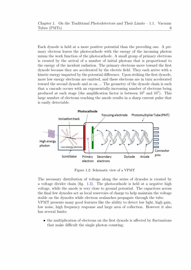
Chapter 1. On the Traditional Photodetectors and Their Limits – 1.1. VacuumTubes (PMTs) 6
Each dynode is held at a more positive potential than the preceding one. A pri-mary electron leaves the photocathode with the energy of the incoming photonminus the work function of the photocathode. A small group of primary electronsis created by the arrival of a number of initial photons that is proportional tothe energy of the incident radiation. The primary electrons move toward the firstdynode because they are accelerated by the electric field. They each arrive with akinetic energy imparted by the potential difference. Upon striking the first dynode,more low energy electrons are emitted, and these electrons are in turn acceleratedtoward the second dynode and so on ... The geometry of the dynode chain is suchthat a cascade occurs with an exponentially-increasing number of electrons beingproduced at each stage (the amplification factor is between 105 and 107). Thislarge number of electrons reaching the anode results in a sharp current pulse thatis easily detectable.
Figure 1.2: Schematic view of a VPMT
The necessary distribution of voltage along the series of dynodes is created bya voltage divider chain (fig. 1.3). The photocathode is held at a negative highvoltage, while the anode is very close to ground potential. The capacitors acrossthe final few dynodes act as local reservoirs of charge to help maintain the voltagestable on the dynodes while electron avalanches propagate through the tube.VPMT presents many good features like the ability to detect low light, high gain,low noise, high frequency response and large area of collection. However it alsohas several limits:
• the multiplication of electrons on the first dynode is affected by fluctuationsthat make difficult the single photon counting;

Chapter 1. On the Traditional Photodetectors and Their Limits – 1.1. VacuumTubes (PMTs) 7
Figure 1.3: Illustrative design of the voltage divider chain of a VPMT
• gain is inversely proportional to linearity4 because of the space charge dis-tribution on the dinodes, therefore linearity decreases with increasing gain;furthermore linearity of signals is affected by several factors related to thestructure of the device such as power supply stability, the divider currentand the cathode resistivity;
• also the time response is affected by significant fluctuations and it is not veryfast (∼ ns) because of the transit time of electrons through the tube that hasa spread depending on structural features of the device such as the numberof dynodes, the photocathode diameter and the overall voltage;
• its sensitivity to magnetic fields limits its range of applications;
• the mechanical structure of dynodes is extremely complex as well as expen-sive;
• it is inefficient in terms of power consumption, since it requires a HV supplyon the cathode (∼ kV) and a PD between one dinode and the next which,moreover, must be calibrated very carefully because it could prejudice thecorrect operation of the detector;
• it presents a bad operation at cryogenic temperatures;
4Proportionality between the early amount of photoelectrons generated by the incident fluxof photons and the final flux reached by the cathode.

Chapter 1. On the Traditional Photodetectors and Their Limits – 1.2.Solid-State Photodetectors 8
• there are many sources of noise that can affect the signal and lead to thegeneration of dark currents and afterpulses: thermionic emission from photo-cathode and dynodes, ohmic leakage between the anode and other electrodesinside the tube, photocurrent produced by scintillation from glass envelope,field emission current, ionization current from residual gases, radiation fromradioisotopes contained in the glass envelope, cosmic rays and environmentalgamma rays.
In order to overcome the problems linked to the dynode chain, research for newphotomultipliers were focused on the use of semiconductors in recent years. Theprogress of these devices has led to the use of reverse p-n junctions to realize solidstate detectors and, then, to the developement of hybrid photomultipliers.
1.2 Solid-State Photodetectors
A considerable alternative to PMTs are the solid-state photodetectors, a new con-stantly developing technology. These devices differ from the vacuum tubes becauseof the working principle. In this case, the amplification mechanism occurs withina solid-state (semiconductor) material, rather than in a vacuum tube [3, 4, 37].Currently the most used are APDs, avalanche photodiodes, P-I-N photodiodes,and the SiPMs, Silicon PhotoMultipliers.Solid-state detectors deserve a separate discussion. Before going into details ofthe key topics of this thesis we believe it is appropriate to introduce some basicnotions about Semiconductor Physics, since it is the necessary theoretical basis forunderstanding the fundamental mechanisms that determine the operating priciplesof the devices of our interest.
1.3 PN Junctions: a Bit of Semiconductor Physics
The ability to conduct current of a material is quantified by its electrical conduc-tivity σ [Ω−1 · cm−1] (or its resistivity ρ [Ω · cm], which identifies the inattidudineto conduct). The conductors have low ρ (10−6 ÷ 10−5[Ω · cm] for silver, copperand aluminum), the insulators have high ρ (glass has ρ = 1010, diamond ρ = 1014,sulfur even ρ = 1017 [Ω · cm]).In electronic application there is need for materials having a behavior not so welldefined, but ductile and versatile. This is due to the fact that the electronic de-vices must be able to allow the current flow in certain conditions, inhibiting it inother and modulate it when necessary.A wide range of materials exist, characterized by intermediate values of ρ, calledsemiconductors. In particular, we consider silicon (Si), a material which has an

Chapter 1. On the Traditional Photodetectors and Their Limits – 1.3. PNJunctions: a Bit of Semiconductor Physics 9
interesting property: its resistivity can be changed ad hoc (even significantly) ina controlled manner [5].A semiconductor in which other atomic species (dopant or impurities) have beenintroduced ad hoc is called extrinsic or doped. Otherwise is called intrinsic or un-doped. The intrinsic silicon can be considered almost an insulator; its resistivityis equal to about 2.5 x 10⁵[Ω · cm] at T = 300 K. This is related to the fact thatin a cm3 of material contains only 1.45 x 10¹⁰ free electrons and holes5, versus 5x 10²² atoms. In electronics is adopted extrinsic silicon, doped with boron (B),arsenic (As), phosphorus (P) and antimony (Sb).Silicon is the most widely used material in the production of semiconductor de-vices. It proceeds from silica, an extremely common material (in nature it is foundin sand, quartz, clay); indeed it constitutes 25% of the earth’s crust. It has a verygood attitude to the formation of surface layers of silicon dioxide (SiO2), whichserves for several uses such as the selective introduction of dopant, the thin oxidegate realization in MOS transistors and circuit protection. The fabrication of sili-con wafers is a standardized process, even for large diameters (20 cm).No other semiconductor material enjoys these properties.Silicon belongs to the group IV of the Periodic Table of Elements, so Si atomis tetravalent. It has 4 valence electrons in the outhermost atom’s energy shell(n = 3), to form covalent bonds with adjacent atoms in the lattice. Its electronconfiguration is the following:
1s22s22p63s23p2 (1.1)
1.3.1 Electronic Band Structure
The electrons of a single, isolated atom occupy atomic orbitals. Each orbitalforms at a discrete energy level. When multiple atoms join together to form into amolecule, their atomic orbitals combine to form molecular orbitals, each of whichforms at a discrete energy level. As more atoms are brought together, the molecularorbitals extend larger and larger, and the energy levels of the molecule will becomeincreasingly dense [7]. Eventually, the collection of atoms form a solid where theenergy levels are so close that they can be considered to form a continuum calleda band.In the crystal lattice of the silicon, where the grating period is 5.43 A, we have twoenergy bands, each of which characterized by N levels energy and 4 x N quantumstates. The lower band is called the valence band; in it the 4 x N quantum statesare all allocated by electrons. The upper band is called the conduction band; in it4 x N quantum states are all empty (fig. 1.4). The middle range is called bandgap,
5Negative and positive charge carriers

Chapter 1. On the Traditional Photodetectors and Their Limits – 1.3. PNJunctions: a Bit of Semiconductor Physics 10
because the corresponding energy levels do not exhibit quantum states allocableby electrons, and has amplitude EG.
Figure 1.4: Si energy band diagram
Figure 1.5 (left) depicts the 2-D representation of the covalent bonds between thesilicon atoms in the crystal lattice.
Figure 1.5: 2-D model of a silicon crystal lattice (left). Release of the electron from the
covalent bond (right)
At temperatures T → 0 K, atoms are fixed in their lattice positions and valenceelectrons are all involved in covalent bonds between 2 silicon atoms, and cannottake part in the conduction phenomenon even in the presence of a local electric
Chapter 1. On the Traditional Photodetectors and Their Limits – 1.3. PNJunctions: a Bit of Semiconductor Physics 11
field E. As temperature increases (T > 0 K) atoms vibrate around their latticesites. Vibrating atoms can be described as a quasi-particle called phonon. Thesephonons interact with electrons involved in covalent bonds (it is said that they”collide”). In such collisions the electrons receive an average energy of the orderof several tens of meV at T = 300 K. This energy is not evenly distributed and,in some cases, it may be sufficient to free an electron from the covalent bond (fig.1.5 right), and let it to take part in the conduction (conduction electrons). Theelectron leaves behind a non saturated covalent bond (a vacancy or a hole) whichis modeled as a fictitious particle with a positive charge equal to the elementarycharge q = 1.602 x 10⁻¹⁹ C. The concentration of free electrons and holes in thelattice increases with temperature T.From the band model point of view, to say that a valence electron is engaged in acovalent bond means that it is allocated in a low energy state or, equivalently, thatit is included in the valence band. The bandgap EG is the minimum energy abovewhich an electron can be released from bonds. To say that an electron is releasedmeans that energy was provided sufficient to let the electron occupy a quantumstate in the conduction band. Typically, the transition is not direct (band-band),but indirect: occurs through quantum states allowed in the bandgap, said G-Rcenters, resulting from impurities and lattice defects (inevitably present).So for T → 0 K all the 4 x N quantum states in the valence band are full (allthe electrons are engaged in covalent bonds) and the 4 x N quantum states in theconduction band are empty (there are no free electron).The importance of the parameter EG in defining the properties of a semiconductoris clear. Its value depends on the particular material and on the temperature (atT = 300 K typical values for insulators and conductors are respectively EG > 3 eVand EG ∼ 0.1 eV ); for silicon EG (T → 0 K) = 1.17 eV and EG (T → 300 K) =1.124 eV. Thus the increase of the concentration of free electrons and holes withincreasing temperature, depends not only on the increase of the vibrational energyof the atoms, but also on the reduction of the bandgap (that is energy required torelease electrons from the bonds).
1.3.2 Direct and Indirect Bandgap
A free electron moving in a crystal lattice, unlike what would happen in a vacuum,is subject to lattice forces (due to interaction with lattice atoms). To treat thisproblem we will appeal to the laws of classical mechanics for a charged particle invacuum, considering the effective mass mk
6 instead of the actual mass me, andthe charge -q.
6Is a quantity that is used to simplify band structures by constructing an analogy to thebehavior of a free particle with that mass. For silicon is mk = 0.26 ·me

Chapter 1. On the Traditional Photodetectors and Their Limits – 1.3. PNJunctions: a Bit of Semiconductor Physics 12
For the free electron in vacuum the dispersion relation7 holds, which binds thekinetic energy to the momentum:
Ekin =1
2
p2
me
. (1.2)
For a free electron within the crystal it is possible to write a similar equation con-sidering the effective mass mk and the crystal momentum (or quasimomentum)instead of the momentum.It is a momentum-like vector associated with electrons in a crystal lattice. It isdefined by the associated wave vectors k of this lattice, according to
p = h · k, (1.3)
where h is the reduced Planck’s constant. It is possible to demonstrate that in theinteractions between electrons, holes, and other quasi-particles (such as photonsand phonons) energy and momentum of the crystal are conserved.It is seen that the energy levels EC (inferior edge of the counduction band) andEV (superior edge of the valence band) are not constant but vary with the crys-tallographic direction and with the quasimomentum.Directions [1 0 0] and [1 1 1] are preferred for the description of the properties ofmaterials, so it is usual to illustrate the trend of EC and EV with respect to thequasimomentum along the latter (fig. 1.6).
Figure 1.6: Trend of EC and EV with respect to the quasimomentum along the crystal-
lographic directions [1 0 0] and [1 1 1] for gallium arsenide and silicon
In figure 1.6 band structures of silicon and gallium arsenide are compared. EV
has a maximum in p = 0 for both gallium arsenide and silicon, while EC has a
7Describes the effect of dispersion in a medium on the properties of a wave traveling withinthat medium

Chapter 1. On the Traditional Photodetectors and Their Limits – 1.3. PNJunctions: a Bit of Semiconductor Physics 13
minimum in p = 0 for the gallium arsenide, and in p 6= 0 for silicon in the direction[1 0 0].EV and EC trends are parabolic in the neighborhood of the maximum and mini-mum and the kinetic energy of a free electron is null when it lies on the minimumof EC (condition that never occurs as we will see later). Free electrons are allo-cated in quantum states in the vicinity of the minimum EC , and not far from theedge EC(p). The bandgap energy corresponds to the distance:
EG = min[EC(p)]−max[EV (p)]. (1.4)
Materials such as gallium arsenide where the minimum of EC and the maximumEV interface for the same quasimomentum are called direct bandgap semicon-ductors, otherwise (such as silicon) they are called indirect bandgap semicon-ductors.It is clear that the following dispersion relations can be written for a free electronin a crystal if we suppose that free electrons are all immediatly near to the edgeof EC(p):
Ekin(GaAs) = E −min[EC(p)] =1
2
p2
mk
, (1.5)
Ekin(Si) = E −min[EC(p)] =1
2
(p− pc)2
mk
. (1.6)
From these equations is inferred that a free electron in silicon has Ekin = 0 ifp = pc. But this condition cannot be achieved, because there are not quantumstates allocable by electrons on the minimum of the conduction band. In bothcases we have:
d2E
dp2=
1
mk
, (1.7)
so this effective mass varies with the curvature of EC . If the curvature is narrow(as for GaAs) then the second derivative is big and mk is small, otherwise (as forSi) mk is bigger:
mk(Si) > mk(GaAs). (1.8)
1.3.3 Statistics of Semiconductors: Fermi Dirac Distribu-tion and the Mass Action Law
A crystal is said to be in thermodynamic equilibrium when it is under steadyconditions and in the absence of electrical loads (d.d.p.) or optical stresses.
Chapter 1. On the Traditional Photodetectors and Their Limits – 1.3. PNJunctions: a Bit of Semiconductor Physics 14
The concentration of available quantum states in the conduction band for theenergy level E has the following expression:
N(E) = γ√
E − EC [cm−3 · eV −1] for E ≥ EC , (1.9)
where γ = 4π 3
√
2mn
h2 . The quantity mn is defined as the electron’s density ofstates effective mass and, for silicon is mn = 1.1 me. In the immediate vicinityof the lower edge of the conduction band there are few quantum states allocatedby electrons, while their concentration increases with increasing energy [8].The concentration of available quantum states in the valence band for the energylevel E has the following expression:
N ′(E) = γ′√
EV − E[cm−3 · eV −1] for E ≤ EV , (1.10)
where γ = 4π 3
√
2mp
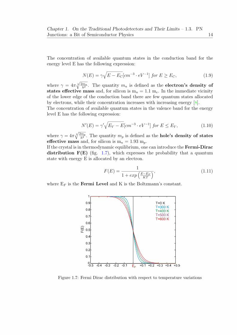
h2 . The quantity mp is defined as the hole’s density of stateseffective mass and, for silicon is mn = 1.93 mp.If the crystal is in thermodynamic equilibrium, one can introduce the Fermi-Diracdistribution F(E) (fig. 1.7), which expresses the probability that a quantumstate with energy E is allocated by an electron.
F (E) =1
1 + exp(
E−EF
KT
) , (1.11)
where EF is the Fermi Level and K is the Boltzmann’s constant.
Figure 1.7: Fermi Dirac distribution with respect to temperature variations

Chapter 1. On the Traditional Photodetectors and Their Limits – 1.3. PNJunctions: a Bit of Semiconductor Physics 15
The Fermi level, is the energy level for which the probability of occupation of aquantum state is 1
2regardless the value of T. It is clear that, for E > EF , the
probability an electron occupies quantum state increases with temperature, whilefor E < EF this probability decreases.This is reasonable if we take into account the fact that the energy of electronsincreases with T, and thus is more likely for electrons to occupy quantum statesat higher energy levels.For T → 0 K the occupation probability is null for E > EF and 1 for E < EF .A similar equation exsists for holes:
F ′(E) = 1− F (E) =1
1 + exp(
EF−EKT
) , (1.12)
that defines the probability that a quantum state at the energy level E is notoccupied by an electron.In intrinsic silicon at T = 300 K we have the following relation:
n = p = ni = 1.45 · 1010cm−3, (1.13)
where p [cm−3] is the hole’s concentration, n [cm−3] is the free electron concentra-tion and ni [cm
−3] is the intrinsic concentration of charge carriers in the lattice.This brings to a resistivity equal to ρ = 2.5 · 105[Ω · cm].On the basis of definitions given below, it is possible to know the total concentra-tion of free electrons and holes expressed in terms of the energy gap between theFermi level and the edge of the conduction and the valence band respectively withthe semiconductor (pure or doped) in termodynamic equilibrium8:
n = NC · exp(
−EC − EF
KT
)
, (1.14)
p = NV · exp(
−EF − EV
KT
)
, (1.15)
where NC is the effective density of states in the conduction band (it is 2.8 x 10¹⁹
cm−3 for silicon at 300K temperature), and NV is is the effective density of statesin the valence band (it is 1.04 x 1019 cm−3 for silicon at 300K temperature). Bymeans of these definitions is now possible to locate the position of the Fermi level
8These expressions come from the fact that the concentration of free electrons (holes) for aenergy interval dE, with E belonging to the conduction (valence) band, is given by the concentra-tion of quantum states can be allocated in the energy range dE (N(E) · dE) times the probability
that they are occupied (F(E)):∫ E0
ECN(E)F (E)dE for electrons and
∫ EV
EVinf
N ′(E)F ′(E)dE fro
holes

Chapter 1. On the Traditional Photodetectors and Their Limits – 1.3. PNJunctions: a Bit of Semiconductor Physics 16
between the valence and conduction bands [6], it is almost in the middle of thebandgap for a pure semiconductor but depends also on the temperature:
EFi=
EC + EV
2− KT
2· lnNC
NV
, (1.16)
Temperature Dependence
Experimentally it is found that NC and NV have a positive temperature coefficientaccording to:
NC(T ) = NC(300K)3
√
T
300K, (1.17)
NV (T ) = NV (300K)3
√
T
300K, (1.18)
In intrinsic silicon at T = 300 K in termodynamic equilibrium we have the followingrelation:
n = p = ni, (1.19)
so by substitution with equations 1.14 and 1.15 we obrain the following expressionfor ni:
n2i = NCNV · exp
(
− EG
KT
)
, (1.20)
With regard to the lattice temperature T dependence, it is clear that ni has apositive temperature coefficient which takes into account two mechanisms:
• increase of the atoms vibrational energy and, therefore, increse of the averageenergy conferred to electrons in covalent bonds;
• bandgap reduction and, therefore, reduction of the minimum energy requiredto release electrons from bonds.
This dependence is expressed as follows:
ni(T ) = A0 · T32 exp
(
− EG0
2KT
)
, (1.21)
where
A0[cm−3 ·K− 3
2 ] =
√
NC(300K)NV (300K) ·(
1
300K
)3
· exp(
γ
K
)
(1.22)

Chapter 1. On the Traditional Photodetectors and Their Limits – 1.3. PNJunctions: a Bit of Semiconductor Physics 17
contains all the temperature sensitive terms, and EG0 = EG(T )+γT is a coefficientwhich comes out from the bandgap decay law9.If we consider the experimental intrinsic concentration for silicon ni(300K) = 1.45x 10⁻¹⁰cm−3, the dependence of ni on the temperature is shown in figure 1.8.
Figure 1.8: Intrinsic concentration trend with respect to temperature variations
It is useful to express the concentrations of free electrons n and holes p in termsof the intrinsic concentration ni by means of the Shockley equations:
n = ni · exp(
−EF − Ei
KT
)
, (1.23)
p = ni · exp(
−Ei − EF
KT
)
, (1.24)
so we can easily derive the mass action law:
p · n =[
ni · exp(
−EF − Ei
KT
)]
·[
ni · exp(
−Ei − EF
KT
)]
= n2i , (1.25)
This product is independent on the Fermi level, which, as will be seen hereinafter,is an indicator of the material doping level; so the product is independent of thetype and level of doping. Indeed it is equal to ni which is a mere function oftemperature.The mass action law expresses the fact that if one tries to increase the concentrationof a certain polarity carriers throug doping, the system reacts by reducing theopposite polarity carriers, so as to preserve the consistency of the product.
9EG(T ) = EG(0)− αT 2
β+Twhere α = 4.73 x 10⁻⁴ [eV/K2] and β = 636 K for silicon

Chapter 1. On the Traditional Photodetectors and Their Limits – 1.3. PNJunctions: a Bit of Semiconductor Physics 18
The law of mass action also describes the fact that higher is the doping, moreunlikely is to break covalent bonds. So the quantity of minority carriers (the lessabundant charge carriers obtained only through the breaking of covalent bonds)decreases as the doping.In general this law is important because in an extrinsic semiconductor at fixedtemperature, being known the concentration of the majority carriers (is almostequal to that of the dopant), one can achieve the concentration of the minoritycarriers.
1.3.4 Doping
It is possible to intentionally contaminate a semiconductor with foreign atoms togive a suitable conductivity to the material, through the enrichment of free chargecarriers of a certain polarity; in this case, the semiconductor is said extrinsic,impure, or doped. The entire development of semiconductor devices was based ondoping.When silicon (tetravalent atom) is doped with trivalent atomic species (boron,gallium and indium), the concentration of holes is increased (and the concentrationof electrons decreases according to the law of mass action).In this case holes are the majority carriers, electrons are the minority carriersand the silicon is said P-type doped.When silicon is doped with pentavalent atomic species (arsenic and phosphorus,but also antimony), in a controlled manner the concentration of electrons increases(and the concentration of holes decreases).In this case electrons are the majority carriers, holes the minority carriers andsilicon is said N-type doped.Dopant atoms ar put into the lattice in substitution of silicon atoms. Typicaldopant concentrations are in the range 1014 ÷ 1020 cm−3. This means that thereare very few impurities compared to silicon atoms (5 x 1022 cm−3); therefore thereis a negligible disturbance of the lattice structure and so band structure is notchanged appreciably.Let us consider N-type silicon doped with arsenic (atomic number 33). The stableconfiguration is reached because arsenic has 5 valence electrons, 4 to form covalentbonds with adjacent silicon atoms (so the octet is reached) and 1 quasi-free10 thatis characterized by an ionization energy equal to EDI ∼ meV (fig. 1.9).At T = 300 K, in intrinsic silicon, only 1.45 x 1010 cm−3 electrons are released fromcovalent bonds by vibrational energy. Since the ionization energy of the quasi-free
10Arsenic atom is modeled as a hydrogen atom, so the ionization energy required to releasethe sigle electron that does not participate in the octet is EDI = 13.6
(11.9)2 · mn
me= 54 meV ≪ EG
= 1.12 eV

Chapter 1. On the Traditional Photodetectors and Their Limits – 1.3. PNJunctions: a Bit of Semiconductor Physics 19
Figure 1.9: 2-D lattice model for silicon doped with arsenic
electrons is in the order of a few tens of meV, their interaction with T = 300 Kvibrating atoms provide for sure enough energy to release them all.In this case we say that the dopant is activated. This means that if in the siliconare introduced in a controlled way 1018 cm−3 arsenic atoms (also called donors),at T = 300 K, there are 1018 cm−3 free electrons in the lattice.In the energy band model we have quantum states can be allocated in the bandgap at a distance EDI = EC - ED
11 ∼ meV from the lower limit of the conductionband, and also called donor’s activation energy.It can be assumed that all these quantum states are roughly at the same energylevel ED because of the fact that the impurities are very few in the host lattice, sothey do not interact between them (there is no intersection between their orbitals)and so in this case the Exclusion Principle does not apply (fig. 1.10).
Figure 1.10: Band model for a N-type silicon lattice
11ED is the energy owned by donor’s electrons

Chapter 1. On the Traditional Photodetectors and Their Limits – 1.3. PNJunctions: a Bit of Semiconductor Physics 20
Let us consider P-type silicon doped with boron (atomic number 5). The stableconfiguration is reached because arsenic has 3 valence electrons to form covalentbonds with adjacent silicon atoms. In this case the octet is not reached since thefourth covalent bond is not formed. Only a few tens of meV is required to makean electron disappears from a Si-Si bond, close to the boron atom, and reappearin the not saturated covalent bond (fig. 1.11).
Figure 1.11: 2-D lattice model for silicon doped with boron
Since the trivalent elements accept an electron from a Si-Si covalent bond they arecalled acceptors. In the energy band model we have quantum states that can beallocated in the band gap at a distance12 EAI = EA - EV ∼ meV from the lowerlimit of the conduction band, and also called acceptor’s activation energy.It can be assumed that all these quantum states are roughly at the same energylevel EA. At T → 0 K all quantum states introduced by the acceptors are empty;with increasing T more and more electrons are accepted from the valence band,resulting in the creation of holes; at T = 300 K all the quantum states are allocatedby electrons (fig. 1.12).
Figure 1.12: Band model for a P-type silicon lattice
12EA is the energy owned by acceptor’s hole

Chapter 1. On the Traditional Photodetectors and Their Limits – 1.3. PNJunctions: a Bit of Semiconductor Physics 21
The Fermi level EF is indicative of the type and concentration of dopant in asemiconductor. It is seen that in the intrinsic silicon is located slightly below thecenter of the band gap.In N-type silicon, a remarkable quantity of electrons is introduced in the conductionband, therefore it is reasonable to think that the function F(E) shifts towardshigher energies, and so EF increases. By contrast, if silicon is P-type, there arefewer free electrons than in intrinsic silicon, and, in addition, the covalent bondsare depleted of electrons; this results in a reduction of F(E) and, therefore, of EF .(fig. 1.13)
Figure 1.13: Fermi level in doped semiconductors
If in a semiconductor occurs the following condition, for which it is heavily doped:
EC − EF ≤ 3kT For N-type , EF − EV ≤ 3kT For P-type (1.26)
it is called degenerate. In a degenerate semiconductor impurities within the hostlattice are so many that their orbitals begin to interact, the Exclusion Principlecomes in, quantum states can not be all at a same energy level and a band ofallowed energy levels in the forbidden band is created. This leads to a reductionof the bandgap (fig. 1.14) with respect to the EG value for a non-degeneratesemiconductor (a phenomenon called band gap narrowing or BGN). The newvalue is given by:
EGeff= EG −∆EG,BGN (1.27)
Chapter 1. On the Traditional Photodetectors and Their Limits – 1.3. PNJunctions: a Bit of Semiconductor Physics 22
Figure 1.14: Phenomenology of the band gap narrowing
Temperature Dependence
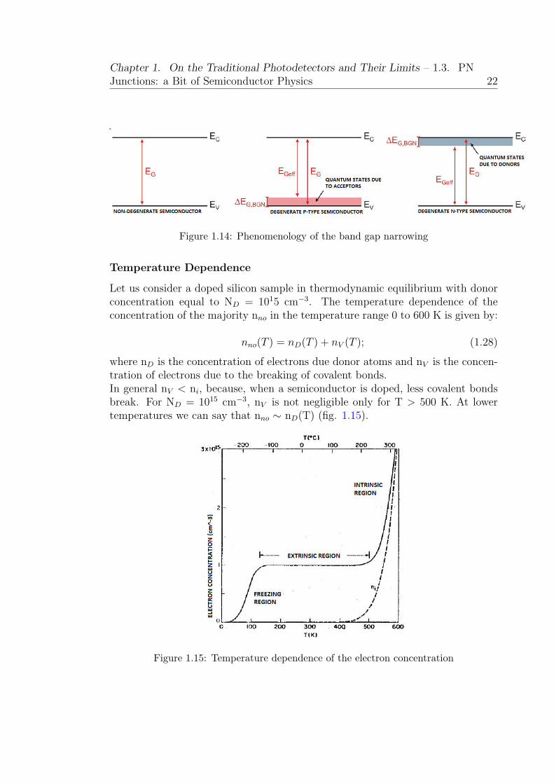
Let us consider a doped silicon sample in thermodynamic equilibrium with donorconcentration equal to ND = 1015 cm−3. The temperature dependence of theconcentration of the majority nno in the temperature range 0 to 600 K is given by:
nno(T ) = nD(T ) + nV (T ); (1.28)
where nD is the concentration of electrons due donor atoms and nV is the concen-tration of electrons due to the breaking of covalent bonds.In general nV < ni, because, when a semiconductor is doped, less covalent bondsbreak. For ND = 1015 cm−3, nV is not negligible only for T > 500 K. At lowertemperatures we can say that nno ∼ nD(T) (fig. 1.15).
Figure 1.15: Temperature dependence of the electron concentration

Chapter 1. On the Traditional Photodetectors and Their Limits – 1.3. PNJunctions: a Bit of Semiconductor Physics 23
For T ≤ 120K we are in the freeze-out regime (or freezing region) where theconcentration of the majority carriers is give by:
nno ∼ ND · (1− F (ED)), (1.29)
where ND is the concentration of quantum states at the energy level ED and (1- F(ED)) is the probability that these states are not filled with electrons. ForT > 120K every donor has given a free electron to the lattice son the electronconcentration is equal to the donor atoms concentration: nD(T) = ND. For 120 K≤ T ≥ 500 K we are in the extrinsic region where the majority concentration isalmost equal to donor atoms concentration: nno(T) ∼ ND. For 500 K ≤ T ≥ 600K we have nno(T) = nD(T) + nV (T) and for T > 600 K we have nV ∼ ni ≫ ND
so nno(T) ∼ ni(T) and it is called intrinsic region.Moreover we can see that the gap EC - EF in estrinsic region (where all impuritiesare activated) increases with temperature according to the following relation:
EC − EF = kT · lnNC(T )
ND
. (1.30)
We expect this kind of effect because as T increases the semiconductor approachesthe intrinsic region, where the Fermi level is close to the band center.If T increases the band gap decreases while if ND increases, the increase of the gapEC - EF becomes slower. Intuitively, for a higher ND more covalent bonds haveto break to bring the semiconductor to the intrinsic region, which means that ahigher temperature is needed to achieve the same value of EC-EF (fig.1.16).
Figure 1.16: Dependence of the bandgap by temperature and concentration of donor
atoms

Chapter 1. On the Traditional Photodetectors and Their Limits – 1.3. PNJunctions: a Bit of Semiconductor Physics 24
1.3.5 Transport and Generation-Recombination Phenom-ena
Two transport phenomena occur in semiconductors: drift and diffusion.When an electric field E is applied across a semiconductor material, a currentis produced due to the flow of charge carriers, it is called drift current and, forelectrons, its density is given by:
Jn,drift = −qnvn, (1.31)
where q is the elementary charge, n is the electron concentration and vn = −µnEis the electron drift velocity (µn is the electron mobility13). For holes a similarrelation holds:
Jp,drift = qpvp, (1.32)
where q is the elementary charge, p is the hole concentration and vp = µpE is thehole drift velocity (µp is the hole mobility). The total drift current density is givenby the sum of these two contributions.Diffusion is the other transport mechanism, is related to the thermal agitation andis due to the change in concentration of the carrier particles in a semiconductorregion; the carriers tend to flow from the higher concentration zone to a lower con-centration zone since it becomes uniform. Diffusion current densities for electronsand holes are given by:
Jn,diff = qDn
dn
dx, Jp,diff = −qDp
dp
dx, (1.33)
where Dn (36 cm2/s for silicon at T= 300K) and Dp (12 cm2/s for silicon at T=300K) are the diffusion coefficients14 (or diffusivity) for electrons and holes respec-tively.The conduction of current in a semiconductor device is due to both these phe-nomena. So the total current densities for electrons and holes is given by the sumof drift and diffusion current densities. In particular, we can obtain EinsteinRelations for electrons and holes from the total current densities expressions inthermodynamic equilibrium conditions:
Jn = qnµnE+ qDn
dn
dx= 0, Jp = qpµpE− qDp
dp
dx= 0, (1.34)
13This parameter characterizes how quickly an electron can move through a semiconductor,when pulled by an electric field.
14It is a proportionality constant between the molar flux due to molecular diffusion and thegradient in the concentration of the species
Chapter 1. On the Traditional Photodetectors and Their Limits – 1.3. PNJunctions: a Bit of Semiconductor Physics 25
Einstein relations link the two significant constants that characterize transport offree carriers in a semiconductor by drift (mobility) and diffusion (diffusivity).
Dn = µn
kT
q, Dp = µp
kT
q. (1.35)
This equation is an early example of a fluctuation-dissipation relation, which isa powerful tool in statistical physics for predicting the behavior of systems thatobey detailed balance [15].Carrier generation and recombination are processes by which electrons andholes are created and eliminated. It occurs when an electron makes transitionfrom the valence band to conduction band, as a result of interaction with otherelectrons, holes, photons, or the vibrating crystal lattice itself. These processesmust conserve both quantized energy and momentum, and the vibrating latticeplays a large role in conserving momentum as photons carry very little momentumin relation to their energy.Recombination and generation are always happening in semiconductors, both op-tically and thermally, and their rates are in balance at equilibrium. The productof the electron and hole densities is a constant at equilibrium (for the mass actionlaw), maintained by recombination and generation occurring at equal rates. Whenthere is a surplus of carriers, the rate of recombination becomes greater than therate of generation, driving the system back towards equilibrium. Likewise, whenthere is a deficit of carriers, the generation rate becomes greater than the recom-bination rate, again driving the system back towards equilibrium. As the electronmoves from one energy band to another, the energy and momentum that it haslost or gained must go to or come from the other particles involved in the process.Depending on which particles are involved in the process, there are different genera-tion ricombination phenomena. They can be direct if the transition occurs directlybetween valence and conduction bands (band-band generation/recombination);they can be indirect if this transition occurs through quantum states allocablein the bandgap, said generation-recombination (G-R) centers or traps, due to im-purities in the lattice (Shockley-Read-Hall process); they can be thermal if theprocess occurs through interactions with phonons; they can be radiative if theprocess involves photons. During radiative recombination, a form of spontaneousemission, a photon is emitted with the wavelength corresponding to the energyreleased. Because the photon carries relatively little momentum, radiative recom-bination is significant only in direct bandgap materials.When photons are present in the material, they can either be absorbed, generatinga pair of free carriers, or they can stimulate a recombination event, resulting in agenerated photon with similar properties to the one responsible for the event. Ab-sorption is the active process in semiconductor photodetectors, so is of particularinterest in this thesis.

Chapter 1. On the Traditional Photodetectors and Their Limits – 1.3. PNJunctions: a Bit of Semiconductor Physics 26
More precisely, let us suppose that a direct bandgap semiconductor is subjectedto a light radiation characterized by frequency ν such that photons meet the ab-sorption condition:
hν > EG. (1.36)
In that case the covalent bond is broken due to the energy provided by the incidentphoton (the electron absorbs the photon). The transition in the band diagram isvertical (fig. 1.17): photon absorption does not imply variations in the electron’squasimomentum.
Figure 1.17: Direct radiative generation in a direct bandgap semiconductor
If the same appens to an indirect bandgap semiconductor, the transition requiresa significant variation of electron’s quasimomentum (fig. 1.18). But since photonsdo not change electron’s quasimomentum, an interaction with the lattice is needed.Being necessary interaction with phonons in addition to photon absorption, thedirect radiative generation occurs rarely with respect to direct bandgap semicon-ductors, which therefore lend themselves more to optical applications.
Figure 1.18: Direct radiative generation in an indirect bandgap semiconductor

Chapter 1. On the Traditional Photodetectors and Their Limits – 1.3. PNJunctions: a Bit of Semiconductor Physics 27
But it is possible to obtain indirect radiative generation, even with an electro-magnetic radiation whose photons do not respect the absorption condition, if thesilicon sample is impure and contains traps (or G-R centers); the electron ab-sorbs the energy of two (or more) photons and interacts with phonons, in this waysmaller variations in the electron’s quasimomentum are required to overcome thebandgap through G-R centers (fig. 1.19).
Figure 1.19: Indirect radiative generation in an indirect bandgap semiconductor
Similar considerations hold for the recombination mechanism.
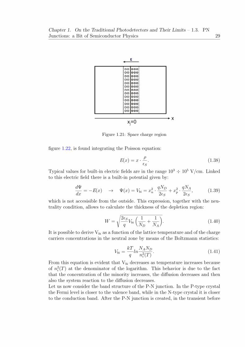
1.3.6 P-N Junction
The P-N junctions are crucial devices in electronics since they are elementarybuilding blocks of most semiconductor devices. A P-N junction is obtained byinterfacing an N-type semiconductor with a P-type semiconductor15, the contactpoint is called ”metallurgical junction” xj.Let us suppose to be in the ideal case, at first charge carriers behave as if they arein two separate crystals in thermodynamic equilibrium. Then, at the boundary, itbegins a diffusion mechanism which brings free charge carriers to migrate to theregions in which they are minority (minority carrier injection); large part of theseinjected carriers is lost by recombination. Both Jn,diff and Jp,diff are reduced overtime. After a certain time interval space charge distributions are changed (fig.1.20).The crystal is still electrically neutral, but the quantity of free carriers was reducedbecause of recombination.A fixed space charge region depleted from mobile carriers, called space chargeregion SCR, is created (fig.1.21) where only the fixed ions (donors or acceptors)remain. The resulting charge dipole induces the presence of a electric field E
(called built-in electric field) directed as -x; the amplitude of dipole charge and
15A P+ implantation in a N doped semiconductor is performed by means of a planar process

Chapter 1. On the Traditional Photodetectors and Their Limits – 1.3. PNJunctions: a Bit of Semiconductor Physics 28
Figure 1.20: Free charge diffusion at the metallurgic junction in a P-N juncion
field increases as the diffusion proceeds. The field E, in turn, generates drift cur-rents which tend to oppose the diffusion currents, gradually reducing the minorityinjection and bringing the system to equilibrium (steady-state condition).Out of the SCR there are the neutral regions where charge carriers behave as if theyare in two separate crystals in thermodynamic equilibrium. In this conditions theP-N junction is said to be open circuited and, being the structure macroscopicallyneutral, there must be the neutrality condition:
xp · qNA = xn · qND, (1.37)
where q NA and q ND are the space charge densities ρ for the P side and the Nside respectively, xp and xn are the thicknesses of the depletion regions for the Pside and the N side respectively. From this equation is evident that if one of thetwo samples is much more doped than the other, for example if NA ≫ ND, thedepletion region will extend only throughout the N-type region.The trend of the built-in electric field through the depletion region, depicted in
Chapter 1. On the Traditional Photodetectors and Their Limits – 1.3. PNJunctions: a Bit of Semiconductor Physics 29
Figure 1.21: Space charge region
figure 1.22, is found integrating the Poisson equation:
E(x) = x · ρ
ǫS. (1.38)
Typical values for built-in electric fields are in the range 103 ÷ 105 V/cm. Linkedto this electric field there is a built-in potential given by:
dΨ
dx= −E(x) → Ψ(x) = Vbi = x2
n ·qND
2ǫS+ x2
p ·qNA
2ǫS, (1.39)
which is not accesisible from the outside. This expression, together with the neu-trality condition, allows to calculate the thickness of the depletion region:
W =
√
2ǫSq
Vbi
(
1
ND
+1
NA
)
. (1.40)
It is possible to derive Vbi as a function of the lattice temperature and of the chargecarriers concentrations in the neutral zone by means of the Boltzmann statistics:
Vbi =kT
qlnNAND
n2i (T )
. (1.41)
From this equation is evident that Vbi decreases as temperature increases becauseof n2
i (T ) at the denominator of the logarithm. This behavior is due to the factthat the concentration of the minority increases, the diffusion decreases and thenalso the system reaction to the diffusion decreases.Let us now consider the band structure of the P-N junction. In the P-type crystalthe Fermi level is closer to the valence band, while in the N-type crystal it is closerto the conduction band. After the P-N junction is created, in the transient before

Chapter 1. On the Traditional Photodetectors and Their Limits – 1.3. PNJunctions: a Bit of Semiconductor Physics 30
Figure 1.22: P-N junction characteristic quantities
the system reach the thermodynamic equilibrium, the potential energy of freeelectrons, i.e., the edge of the conduction band EC(x), can no longer be uniform,because of the presence of the quadratic potential Ψ(x)16. In particular in the Pside we have the minimum of the potential energy (0) and in the N side we havethe maximum (-qVbi).Since the system is at equilibrium, the Fermi level should be uniform throughoutthe material. Furthermore, far from the junction, there are two simple P-typeand N-type semiconductors, so EFP
− EV and EC− EFNmust be constant in the
two sides respectively. Since even the bandgap EG has to be constant throughoutthe system, this results in a band bending close to the junction point (fig. 1.23)according to the following equations:
16The potential energy of a charged particle varies as -qΨ(x)

Chapter 1. On the Traditional Photodetectors and Their Limits – 1.3. PNJunctions: a Bit of Semiconductor Physics 31
EC(x) = ECP− qΨ(x), EV (x) = EVP
− qΨ(x) (1.42)
Figure 1.23: Band bending at the metallurgical junction in a P-N junction
This bending results in the creation of a potential barrier of height Vbi, whichprevents the minority carriers injection.The free electrons that drift from the neutral region P to N are few (because theyare the minority carriers); they lose and regain kinetic energy in the SCR becauseof lattice collisions and the presence of the built-in field E.The free electrons that diffuse from the neutral region N to P are few (becauseof the potential barrier); the situation is such that the flow of drift (P → N) anddiffusion (N → P) electrons are balanced (fig. 1.24); in general Jn,drift and Jn,diffare high (in modulus are the same) since E and the gradient dn/dx in the SCRare high.
Figure 1.24: Drift and diffusion at the metallurgical junction in a P-N junction
Chapter 1. On the Traditional Photodetectors and Their Limits – 1.3. PNJunctions: a Bit of Semiconductor Physics 32
1.3.7 Forward Biasing
When a junction is connected to a potential difference (PD) V, such as V > Vγ17,
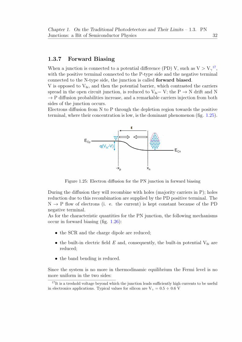
with the positive terminal connected to the P-type side and the negative terminalconnected to the N-type side, the junction is called forward biased.V is opposed to Vbi, and then the potential barrier, which contrasted the carriersspread in the open circuit junction, is reduced to Vbi− V; the P → N drift and N→ P diffusion probabilities increase, and a remarkable carriers injection from bothsides of the junction occurs.Electrons diffusion from N to P through the depletion region towards the positiveterminal, where their concentration is low, is the dominant phenomenon (fig. 1.25).
Figure 1.25: Electron diffusion for the PN junction in forward biasing
During the diffusion they will recombine with holes (majority carriers in P); holesreduction due to this recombination are supplied by the PD positive terminal. TheN → P flow of electrons (i. e. the current) is kept constant because of the PDnegative terminal.As for the characteristic quantities for the PN junction, the following mechanismsoccur in forward biasing (fig. 1.26):
• the SCR and the charge dipole are reduced;
• the built-in electric field E and, consequently, the built-in potential Vbi arereduced;
• the band bending is reduced.
Since the system is no more in thermodinamic equilibrium the Fermi level is nomore uniform in the two sides:
17It is a treshold voltage beyond which the junction leads sufficiently high currents to be usefulin electronics applications. Typical values for silicon are Vγ = 0.5 ÷ 0.6 V

Chapter 1. On the Traditional Photodetectors and Their Limits – 1.3. PNJunctions: a Bit of Semiconductor Physics 33
Figure 1.26: Characteristic quantities for the PN junction in forward biasing
EFN− EFP
= qV (1.43)
The total current flowing through the junction is described by the Shockley equa-tion:
I = IS
[
exp
(
qV
ηkT
)
− 1
]
, (1.44)
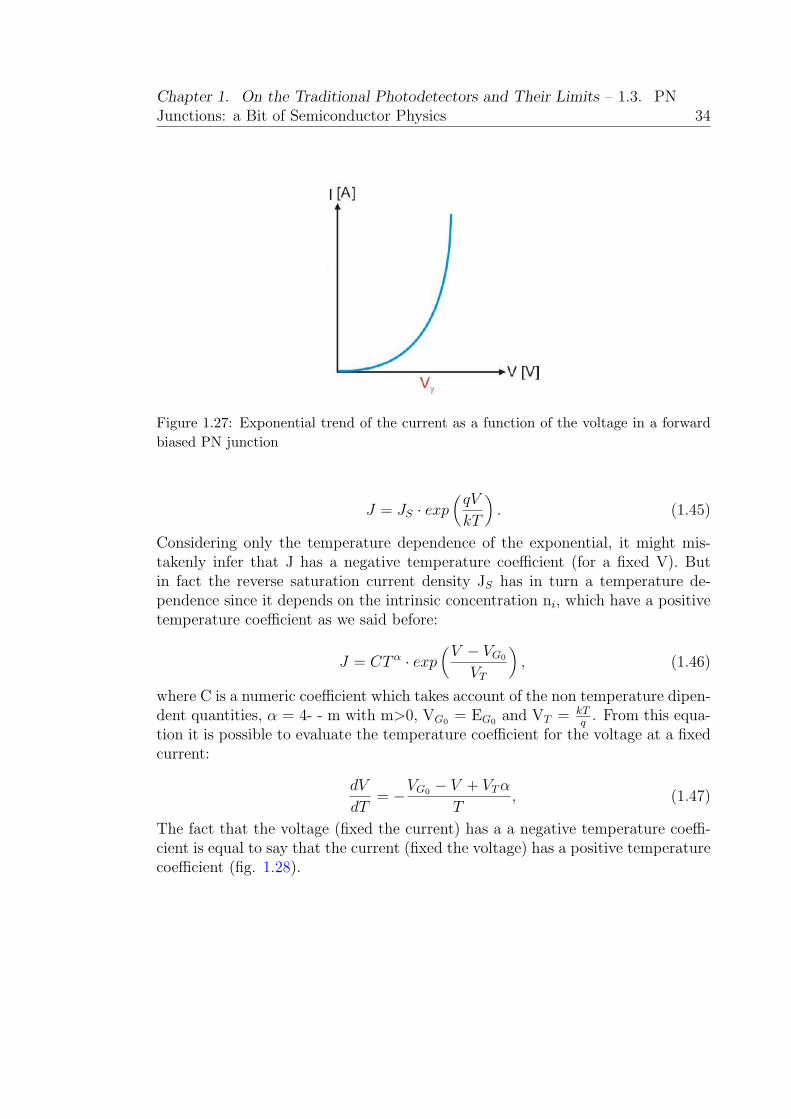
where η is the ideal factor of the diode and is about 1 for germanium and about 2for silicon; IS is the inverse saturation current, which describes the diffusion flowof the minority carrier. Because at 25C temperature kT/q ∼ 0,025V, it is clearthat in forward biasing for a PD of the order of 0.1V, the 1 can be neglected withrespect to the exponential term, so the current increases exponentially with thevoltage [9]. Figure 1.27 shows this trend.
Temperature dependence
In terms of current density J[A/µm2] we have:
Chapter 1. On the Traditional Photodetectors and Their Limits – 1.3. PNJunctions: a Bit of Semiconductor Physics 34
Figure 1.27: Exponential trend of the current as a function of the voltage in a forward
biased PN junction
J = JS · exp(
qV
kT
)
. (1.45)
Considering only the temperature dependence of the exponential, it might mis-takenly infer that J has a negative temperature coefficient (for a fixed V). Butin fact the reverse saturation current density JS has in turn a temperature de-pendence since it depends on the intrinsic concentration ni, which have a positivetemperature coefficient as we said before:
J = CT α · exp(
V − VG0
VT
)
, (1.46)
where C is a numeric coefficient which takes account of the non temperature dipen-dent quantities, α = 4- - m with m>0, VG0 = EG0 and VT = kT
q. From this equa-
tion it is possible to evaluate the temperature coefficient for the voltage at a fixedcurrent:
dV
dT= −VG0 − V + VTα
T, (1.47)
The fact that the voltage (fixed the current) has a a negative temperature coeffi-cient is equal to say that the current (fixed the voltage) has a positive temperaturecoefficient (fig. 1.28).

Chapter 1. On the Traditional Photodetectors and Their Limits – 1.3. PNJunctions: a Bit of Semiconductor Physics 35
Figure 1.28: Temperature dependence of the current as a function of the voltage in a
forward biased PN junction
1.3.8 Reverse Biasing And Impact Ionization Theory
If the N-region of the junction is connected to the positive terminal of a PD andthe P-region to the negative terminal, the junction is said to be reverse biased.In this condition, the majority carriers, attracted by the PD the terminals, areremoved from the metallurgical junction; this results in a SCR enlargement. Thevoltage applied VR raises the potential barrier to Vbi+ VR and the electric fieldwithin the depletion region increases. The few holes of the N-region are extractedand migrate quickly through the junction towards the P-side. The same happensfor the electrons, that migrate from P to N because of the electric field. So thereis a minority carriers flux crossing the junction (fig. 1.29); this current, IS, isthe reverse saturation current we have seen before. This current is a construc-tive parameter and depends on the characteristics of the particular semiconductormaterial, the nature and concentration of impurities and on the temperature.
Figure 1.29: Electron drift for the PN junction in reverse biasing
Chapter 1. On the Traditional Photodetectors and Their Limits – 1.3. PNJunctions: a Bit of Semiconductor Physics 36
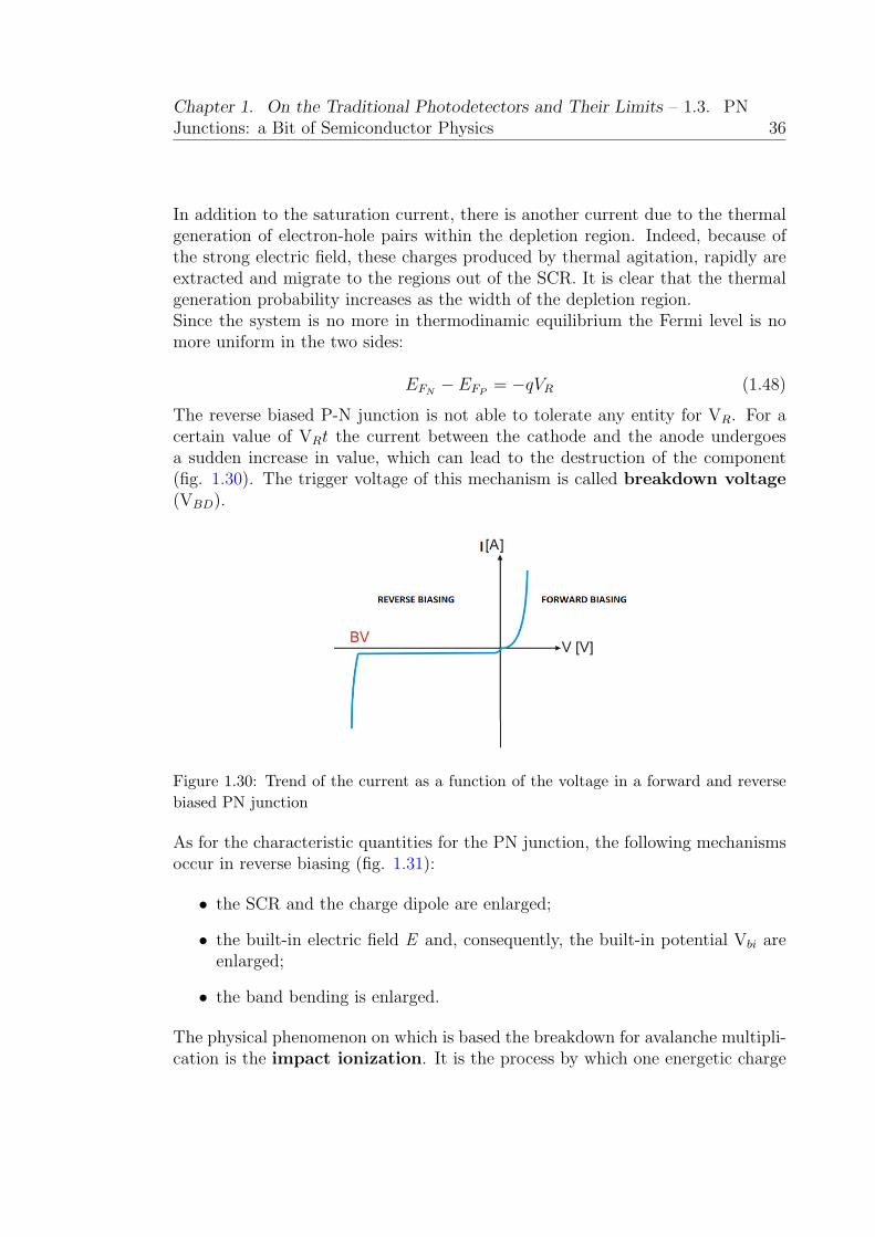
In addition to the saturation current, there is another current due to the thermalgeneration of electron-hole pairs within the depletion region. Indeed, because ofthe strong electric field, these charges produced by thermal agitation, rapidly areextracted and migrate to the regions out of the SCR. It is clear that the thermalgeneration probability increases as the width of the depletion region.Since the system is no more in thermodinamic equilibrium the Fermi level is nomore uniform in the two sides:
EFN− EFP
= −qVR (1.48)
The reverse biased P-N junction is not able to tolerate any entity for VR. For acertain value of VRt the current between the cathode and the anode undergoesa sudden increase in value, which can lead to the destruction of the component(fig. 1.30). The trigger voltage of this mechanism is called breakdown voltage(VBD).
Figure 1.30: Trend of the current as a function of the voltage in a forward and reverse
biased PN junction
As for the characteristic quantities for the PN junction, the following mechanismsoccur in reverse biasing (fig. 1.31):
• the SCR and the charge dipole are enlarged;
• the built-in electric field E and, consequently, the built-in potential Vbi areenlarged;
• the band bending is enlarged.
The physical phenomenon on which is based the breakdown for avalanche multipli-cation is the impact ionization. It is the process by which one energetic charge

Chapter 1. On the Traditional Photodetectors and Their Limits – 1.3. PNJunctions: a Bit of Semiconductor Physics 37
Figure 1.31: Characteristic quantities for the PN junction in reverse biasing
carrier can lose energy by the creation of other charge carriers. In particular, anelectron (or hole) with enough kinetic energy can knock a bound electron out ofits bound state (in the valence band) and promote it to a state in the conductionband, creating an electron-hole pair.If VR is very high, and so the built-in electrical field E, in their mean free path elec-trons can acquire kinetic energy > EG. Impacting with covalent bonds, they arethen able to create free electron-hole pairs, which, in turn, can impact the latticeand create other couples [10]; this results in a so called avalanche breakdown(fig. 1.32).A P-N junction can work in the breakdown regime by means of avalanche mul-tiplication. This mechanism is relevant for this thesis since it is fundamental tothe understanding of the operation of avalanche photodiodes (APD) and SiliconPhotomultipliers.The avalanche multiplication phenomenon in semiconductor junctions was studiedfor the first time by K. G. McKay in 1953, which proposed a model inspirated tothe Townsend discharge model [13].It is possible to define the ionization rate of electrons in a semiconductor junction,
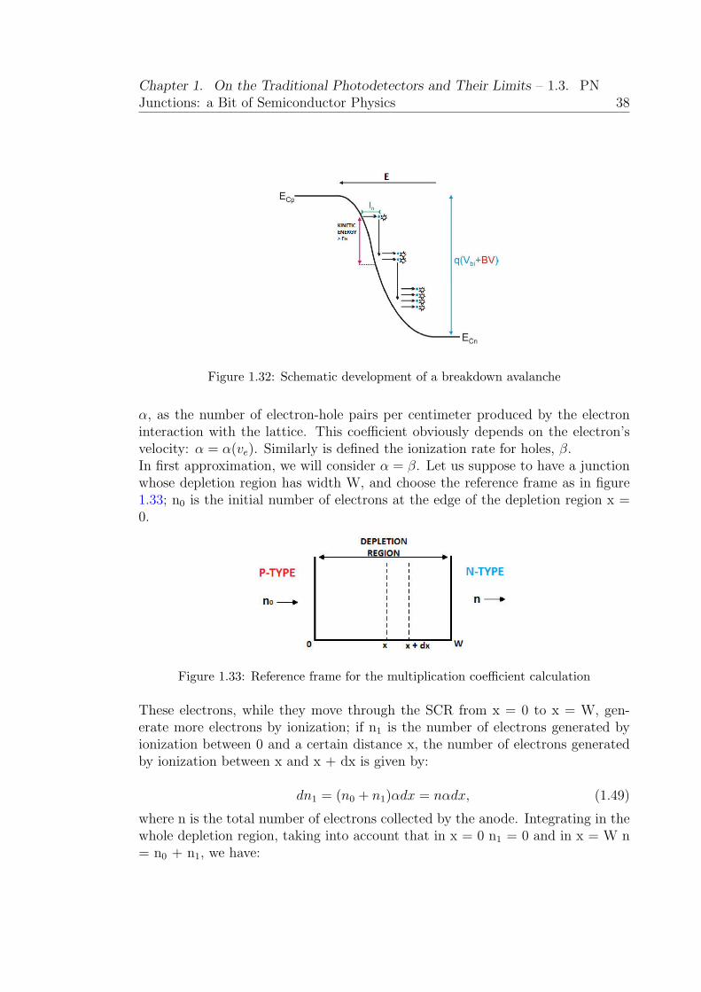
Chapter 1. On the Traditional Photodetectors and Their Limits – 1.3. PNJunctions: a Bit of Semiconductor Physics 38
Figure 1.32: Schematic development of a breakdown avalanche
α, as the number of electron-hole pairs per centimeter produced by the electroninteraction with the lattice. This coefficient obviously depends on the electron’svelocity: α = α(ve). Similarly is defined the ionization rate for holes, β.In first approximation, we will consider α = β. Let us suppose to have a junctionwhose depletion region has width W, and choose the reference frame as in figure1.33; n0 is the initial number of electrons at the edge of the depletion region x =0.
Figure 1.33: Reference frame for the multiplication coefficient calculation
These electrons, while they move through the SCR from x = 0 to x = W, gen-erate more electrons by ionization; if n1 is the number of electrons generated byionization between 0 and a certain distance x, the number of electrons generatedby ionization between x and x + dx is given by:
dn1 = (n0 + n1)αdx = nαdx, (1.49)
where n is the total number of electrons collected by the anode. Integrating in thewhole depletion region, taking into account that in x = 0 n1 = 0 and in x = W n= n0 + n1, we have:
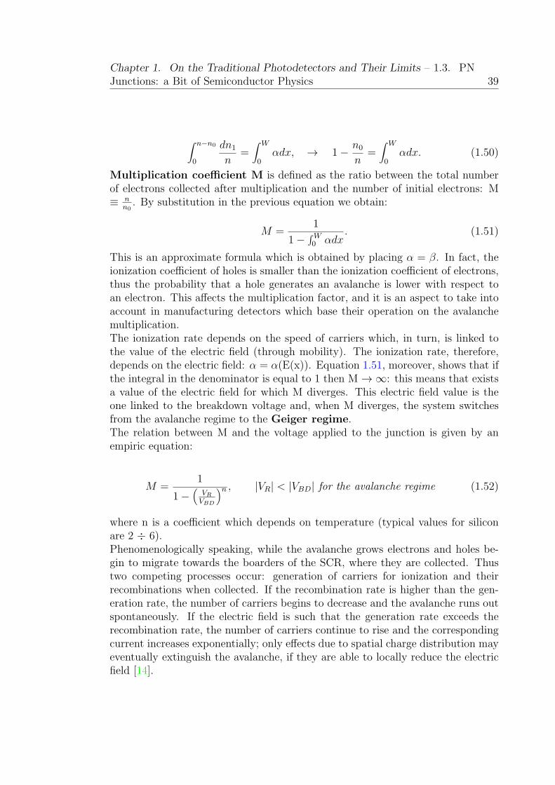
Chapter 1. On the Traditional Photodetectors and Their Limits – 1.3. PNJunctions: a Bit of Semiconductor Physics 39
∫ n−n0
0
dn1
n=∫ W
0
αdx, → 1− n0
n=∫ W
0
αdx. (1.50)
Multiplication coefficient M is defined as the ratio between the total numberof electrons collected after multiplication and the number of initial electrons: M≡ n
n0. By substitution in the previous equation we obtain:
M =1
1− ∫W0 αdx
. (1.51)
This is an approximate formula which is obtained by placing α = β. In fact, theionization coefficient of holes is smaller than the ionization coefficient of electrons,thus the probability that a hole generates an avalanche is lower with respect toan electron. This affects the multiplication factor, and it is an aspect to take intoaccount in manufacturing detectors which base their operation on the avalanchemultiplication.The ionization rate depends on the speed of carriers which, in turn, is linked tothe value of the electric field (through mobility). The ionization rate, therefore,depends on the electric field: α = α(E(x)). Equation 1.51, moreover, shows that ifthe integral in the denominator is equal to 1 then M → ∞: this means that existsa value of the electric field for which M diverges. This electric field value is theone linked to the breakdown voltage and, when M diverges, the system switchesfrom the avalanche regime to the Geiger regime.The relation between M and the voltage applied to the junction is given by anempiric equation:
M =1
1−(
VR
VBD
)n , |VR| < |VBD| for the avalanche regime (1.52)
where n is a coefficient which depends on temperature (typical values for siliconare 2 ÷ 6).Phenomenologically speaking, while the avalanche grows electrons and holes be-gin to migrate towards the boarders of the SCR, where they are collected. Thustwo competing processes occur: generation of carriers for ionization and theirrecombinations when collected. If the recombination rate is higher than the gen-eration rate, the number of carriers begins to decrease and the avalanche runs outspontaneously. If the electric field is such that the generation rate exceeds therecombination rate, the number of carriers continue to rise and the correspondingcurrent increases exponentially; only effects due to spatial charge distribution mayeventually extinguish the avalanche, if they are able to locally reduce the electricfield [14].

Chapter 1. On the Traditional Photodetectors and Their Limits – 1.3. PNJunctions: a Bit of Semiconductor Physics 40
So finally, in an avalanche junction the applied reverse voltage is lower than thethe breakdown voltage and the average number of carriers generated by ionization,≪ ∞, is calculated from 1.51; while, in a Geiger junction the reverse voltage ap-plied is higher than the the breakdown voltage and the number of carriers growsexponentially. To make a Geiger junction usable, an external mechanism thatallows to turn off the avalanche is mandatory.
1.3.9 Transition Capacitance
The depletion region of a open circuit P-N junction, consists of positive and neg-ative fixed charges at a distance equal to the width W of the SCR. So it is similarto a plane capacitor. Denoting by A the cross section of junction, the total chargein the depletion region is Q = qNDWNA in the N side and -Q = -qNAWPA in theP side. The width of the SCR is a function of Vbi. When the junction is polarized,Vbi changes, then W changes, and consequently there is a charge accumulation.It is useful to define a incremental capacity, which relates the voltage increase withthe the accumulated charge increase. It is defined as the transition capacitanceand is given by:
CT ≡ dQ
dV. (1.53)
For an open circuit junction the width of the SCR is given by:
W =
√
2ǫVbi(NA +ND)
qNAND
. (1.54)
If an external PD V occurs it becomes:
W =
√
2ǫ(Vbi − V )(NA +ND)
qNAND
. (1.55)
So the transition capacitance can be obtained as a function of dopant concentra-tions:
CT =ǫA
W=
A√
(Vbi − V )
√
qNAND
2ǫ(NA +ND). (1.56)
Notice that if V<0 (reverse biasing case) W increases and CT decreases (typ. ∼pF)

Chapter 1. On the Traditional Photodetectors and Their Limits – 1.4.Junctions as Radiation Detectors 41
1.4 Junctions as Radiation Detectors
A simple P-N junction can operate as a radiation detector, if at the two sides areapplied two metal contacts: the radiation that passes through the depletion regionmay transfer enough energy to the material to generate electron-hole pairs. Thedrift of these carriers under the action of the electric field generates a current.This current lasts as long as carriers reach the limit of the depletion region, whenthey recombine on the electrodes.The average energy required for a ionizing particle to create a pair is ∼ 3 eVin silicon, and weakly dependent on temperature and on the nature of incidentradiations. Notice that this energy is much greater than the bandgap (1.12 eV forsilicon), so most of it is spent on vibrations of the crystal lattice.However, using a non-biased junction as a detector is not the ideal solution.First, the electric field in the depletion region (also called active zone when usedas detectors) is not intense enough to ensure an efficient collection of carriers, andthus a part of them is lost for recombination before it can reach the electrodes.Furthermore, the active region is small.This creates two issues: only low energy particles can stay in the material (and thislimits the measurement possibilities), and it is difficult to produce enough pairsto form a signal that can be distinguished from noise (due to thermal generationof pairs within the SCR; the high conductivity of the neutral regions favors thepassage of this background current).This results in an inefficient, very noisy detector which is also hard to implementin an electronic amplification circuit.Reverse biased junction is the solution because of the enlargement of the activezone (in silicon, ∼5mm for a reverse biased junction versus∼ 75µm for a non-biasedjunction). Because of the recombination, in the depletion region the intrinsicconcentration of the charge carriers is equal to that of the intrinsic silicon (1.45 x1010 cm−3 at T=300K) which involves a very high resistivity (2.5 x 10⁵ Ω · cm).The high resistivity causes a higher voltage drop across the depletion region and anincrease of the electric field inside it (E ≥ 105 V/cm). This results in an increaseof the impact ionization coefficient which leads to the production of an outputcurrent signal large enough to not need a particularly complex additional externalamplifier (fig. 1.34).Thanks to the many advantages they offer (low average energy required for pairsproduction, small size, low costs) in the 50s semiconductors are been widely usedin the detection of radiation, both ionizing (beta, fast electrons and heavy ions)and electromagnetic (photons) [11].In the following sections we will describe the most used configurations.

Chapter 1. On the Traditional Photodetectors and Their Limits – 1.5. P+-N,P-N+ Junctions and Photodiodes 42
Figure 1.34: Resisitivity of the depletion region in a reverse biased p-n junction
1.5 P+-N, P-N+ Junctions and Photodiodes
In the P-N+ configuration (fig. 1.35), the N-side is much more doped than theP-side, so the depletion region is almost all located in the P-side.
Figure 1.35: P-N+ junction with the electric field trend into the depletion region [12]
The supply voltage is selected so that the active area fully covers the P side. Inthis case the detector is completely depleted, with a remarkable reduction of noise(since there are no more neutral regions).A radiation impinging the depletion region creates electron-hole pairs. The chargesmigrate under the action of the electric field inducing a variation in the electrodescharge. This variation is given by:

Chapter 1. On the Traditional Photodetectors and Their Limits – 1.5. P+-N,P-N+ Junctions and Photodiodes 43
dQ =q
ddx, (1.57)
where dx is the distance traveled and d is the distance between electrodes. Ap-propriately integrating this quantity, it is possible to calculate the total chargecollected on the two electrodes for one electron and one hole:
QTOT = − q
Wx0
(
1− W
x0
)
+q
Wx0, → QTOT = q, (1.58)
and not 2q as expected (Ramo’s law). The total charge collected after the passageof a particle depends on the number of pairs created, on the particle trajectoryand on variations of the electric field within the active area; it is therefore verydifficult to calculate.For the P+-N type similar considerations hold and lead to the same result.Very often, this second type is used as the photodetector, and it is called a photo-diode (fig. 1.36). Light pours in the detector through the P+ side, which for thisreason is provided with a no-reflecting window (typically Si3N4 is used as windowmaterial) to reduce the loss of photons by reflection.
Figure 1.36: Schematic view of a photodiode
Then photons are absorbed and, to produce electron-hole pairs, their energy mustbe greater than EG, so hν = hc
λ> EG.
This costraint introduces a cutoff wavelength, above which the photons are nolonger absorbed by the detector:
λG(µm) =1.24µmeV
EG eV(1.59)
For silicon, EG= 1.12eV and therefore would be λG = 1.11µm. But in fact, sincethe silicon is a indirect bandgap semiconductor, the photon absorption must occur

Chapter 1. On the Traditional Photodetectors and Their Limits – 1.5. P+-N,P-N+ Junctions and Photodiodes 44
even through the lattice vibrations. If θ is the frequency of lattice vibrations andthe phonon energy is hθ, the photon will be absorbed only if hν > EG ± hθ holds.However, usually θ is neglectet since, in silicon, it is very small (<0.1eV).Another important feature in photodiodes is the material’s absorption coefficient:when the photons penetrate the detector, their number decreases exponentiallywith time. Therefore, light intensity at a distance x from the semiconductor’ssurface is given by:
I(x) = I0exp(−αx), (1.60)
where α is the absorption coefficient, a parameter which depends on the particularmaterial. Its inverse is called ”penetration depth” and is the distance within 63% ofincident photons are absorbed. In manufacturing a photodiode, it must be chosena material whose penetration depth is of the same size of the depletion regionin correspondence to the wavelength to be detected. Indeed, if the absorptioncoefficient is too large, photons are absorbed in the P+ layer where there is noelectric field and then the pairs generated quickly recombine. If, instead, theabsorption coefficient is too small, a few photons are absorbed in the depletionregion and thus a few pairs are generated, this results in a small signal that cannotbe distinguished from noise.In particular, silicon is an excellent visible light detector.For the photodiodes quantum efficiency QE is defined the ratio of the number ofpairs produced and collected and the number of incident photons18:
QE =e-h pairs
Incident photons< 1. (1.61)
Another fundamental quantity is the spectral responsivity of the photodiode, de-fined as the relationship between the photocurrent generated and the incidentoptical power. Figure 1.37 shows the plot of the spectral response of a siliconphotodiode as a function of the wavelength, and is compared with that of an idealphotodiode with QE = 1.
18QE is always less than 1 because of carriers recombination, photon reflections on the detec-tor’s surface and effects due to α

Chapter 1. On the Traditional Photodetectors and Their Limits – 1.5. P+-N,P-N+ Junctions and Photodiodes 45
Figure 1.37: Comparison between the spectral response of a realistic photodiode and an
ideal photodiode
Advantages compared to PMTs:
• Excellent linearity of output current as a function of incident light;
• Spectral response from 190 nm to 1100 nm (silicon), longer wavelengths withother semiconductor materials;
• Low noise;
• Ruggedized to mechanical stress;
• Low cost;
• Compact and light weight;
• Long lifetime;
• High quantum efficiency (typically 60 ÷ 80%);
• No high voltage required.
Disadvantages compared to PMTs:
• Small area;
• No internal gain;
• Much lower overall sensitivity;

Chapter 1. On the Traditional Photodetectors and Their Limits – 1.6. Si(Li)And P-I-N Detectors 46
• Photon counting only possible with specially designed, usually cooled pho-todiodes, with special electronic circuits;
• Response time for many designs is slower;
• Latent effects.
1.6 Si(Li) And P-I-N Detectors
In some applications, the detection of long wavelength photons, the width of astandard photodiode the depletion region is often not enough. A different con-figuration is used, consisting of two high doped layers separated by an intrinsiclayer. Usually this structures are obtained by treating silicon doped layers withlithium atoms by means of the doping for overcompensation technique (thereforethe detector is said Si(Li): lithium drifted silicon).The resulting P-N junction is then reverse biased and brought to high tempera-ture to raise the mobility of donor atoms: driven by the electric field, donors moveslowly in the P layer and their concentration increases until it is equal to accep-tors concentration (this operation is also called compensation, and the materialobtained is called a compensated semiconductor).
Figure 1.38: Schematic view of a Si(Li) detector
The result of this process is shown in figure 1.38, a large compensated material layer(very similar to a intrinsic semiconductor) is located between a N+ layer, (obtainedby overcompensation) which is used as electrode, and P, (the non compensatedlayer) on which is deposited a metal layer to make the second electrode.In the ideal case there is no space charge density within the compensated layerI, therefore, its internal electric field is constant; in the absence of polarizationthe contact potential value is fixed to Ebi. When a reverse voltage is applied theelectric field becomes:

Chapter 1. On the Traditional Photodetectors and Their Limits – 1.6. Si(Li)And P-I-N Detectors 47
E = Ebi +VR
W, (1.62)
and it continues to be constant throughout the region, unlike the case of simpleP-N junction. Depletion region of N+ and P layers can be neglected since theseare very thin with respect to I, then the width of the active area is equal to thewidth of I layer.The transition capacitance does not depend on the applied voltage, unlike the P-Njunction.The mechanism for particle detection is the same as in the P-N junction: the radi-ation penetrates into the compensated layer producing pairs which are separatedby the electric field and collected at the electrodes.The difference is in the width of the active region (even 10 mm) that makes thisdevice very suitable for accurate energy measurements and detection of beta par-ticles.Semiconductors in such a configuration are used as photodetectors. They are calledP-I-N photodiodes (fig. 1.39). In this case also the P layer is highly doped andon it is placed a window coated with anti-reflection material, through which lightpenetrates. The wide depletion region enables these photodetectors to obtain amuch more high quantum efficiency; but, of course, carriers generated in the I layerhave to travel a greater distance before they reach the electrodes. This makes theP-I-N photodiodes slower compared to P-N junction detectors.
Figure 1.39: Schematic view of a P-I-N photodiode
Avantages and limits of this device with respect to PMTs are similar to P-N junc-tion detectors.The most serious defect of P-I-N and P-N junction photodiodes is that the pho-
Chapter 1. On the Traditional Photodetectors and Their Limits – 1.7.Avalanche Photodiodes: APDs 48
tocurrent produced is very small; this necessitates the use of a complex front endelectronics to amplify these signals, which is often undesirable.A huge step forward in the development of semiconductor detectors was the idea tomake P-N junctions work in their breakdown regime, building structures in whichelectrons and holes during their drift are accelerated to the point that they cantrigger a Geiger avalanche.The use of a semiconductor detector with an internal gain has two huge advantageswith respect P-I-N and P-N junction: remarkably increases the charge collection,and then the signal amplitude, so no amplification circuit is needed, and have afaster response.Such devices are called SPAD (single-photon avalanche diode also known as G-APD) and will be described in detail in next sections, being the basic element ofthe Silicon Photomultiplier, that is the core of this thesis.
1.7 Avalanche Photodiodes: APDs
APDs are high-speed and high sensitivity silicon devices. These features makeAPDs suitable for a wide variety of applications requiring a high sensitivity alsoin low level light detection [18]. Such a device consists of a pn junction with areverse bias voltage which allows to activate the internal avalanche mechanismthat determines the gain. The middle panel of figure 1.40 shows schematically thetypical p+ - p - n construction of an APD. The structure is externally reverse-biased by Vbias, which, together with the intrinsic electric field of the p-n junction,creates an electric field whose strength profile is schematically shown in the toppanel. The field is maximum at the metallurgical junction.Referring to the figure, light is incident on the p+ side. If the energy of light isgreater than the band gap energy EG of the semiconductor used to manufacturethe APD (typically silicon with EG = 1.1 eV), an intrinsic photoelectric effectcan occur producing e-h pairs. Owing to its indirect band structure, the photonabsorption process in silicon also involves a phonon19. The characteristic depth ofphoton absorption depends on the type of the semiconductor and the wavelengthof light. The bottom panel of figure 1.40 shows schematically that the flux Φ of redphotons attenuates less with depth compared to the flux of blue photons. Morespecifically, photon flux Φ(λ, z) as a function of depth z is given by the followingequation
Φ(λ, z) = Φ(λ, 0) · e−αz. (1.63)
19A quantized lattice vibration
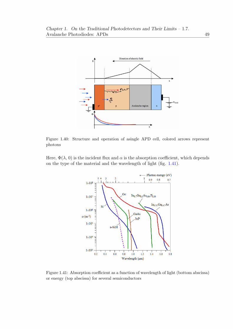
Chapter 1. On the Traditional Photodetectors and Their Limits – 1.7.Avalanche Photodiodes: APDs 49
Figure 1.40: Structure and operation of asingle APD cell, colored arrows represent
photons
Here, Φ(λ, 0) is the incident flux and α is the absorption coefficient, which dependson the type of the material and the wavelength of light (fig. 1.41).
Figure 1.41: Absorption coefficient as a function of wavelength of light (bottom abscissa)
or energy (top abscissa) for several semiconductors
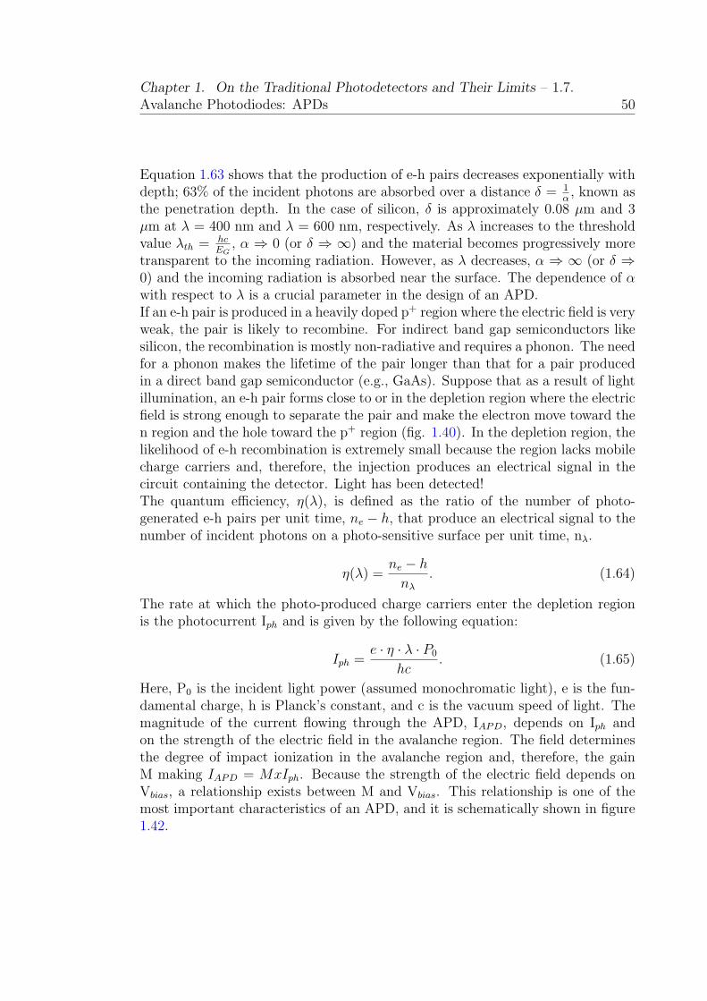
Chapter 1. On the Traditional Photodetectors and Their Limits – 1.7.Avalanche Photodiodes: APDs 50
Equation 1.63 shows that the production of e-h pairs decreases exponentially withdepth; 63% of the incident photons are absorbed over a distance δ = 1
α, known as
the penetration depth. In the case of silicon, δ is approximately 0.08 µm and 3µm at λ = 400 nm and λ = 600 nm, respectively. As λ increases to the thresholdvalue λth = hc
EG, α ⇒ 0 (or δ ⇒ ∞) and the material becomes progressively more
transparent to the incoming radiation. However, as λ decreases, α ⇒ ∞ (or δ ⇒0) and the incoming radiation is absorbed near the surface. The dependence of αwith respect to λ is a crucial parameter in the design of an APD.If an e-h pair is produced in a heavily doped p+ region where the electric field is veryweak, the pair is likely to recombine. For indirect band gap semiconductors likesilicon, the recombination is mostly non-radiative and requires a phonon. The needfor a phonon makes the lifetime of the pair longer than that for a pair producedin a direct band gap semiconductor (e.g., GaAs). Suppose that as a result of lightillumination, an e-h pair forms close to or in the depletion region where the electricfield is strong enough to separate the pair and make the electron move toward then region and the hole toward the p+ region (fig. 1.40). In the depletion region, thelikelihood of e-h recombination is extremely small because the region lacks mobilecharge carriers and, therefore, the injection produces an electrical signal in thecircuit containing the detector. Light has been detected!The quantum efficiency, η(λ), is defined as the ratio of the number of photo-generated e-h pairs per unit time, ne − h, that produce an electrical signal to thenumber of incident photons on a photo-sensitive surface per unit time, nλ.
η(λ) =ne − h
nλ
. (1.64)
The rate at which the photo-produced charge carriers enter the depletion regionis the photocurrent Iph and is given by the following equation:
Iph =e · η · λ · P0
hc. (1.65)
Here, P0 is the incident light power (assumed monochromatic light), e is the fun-damental charge, h is Planck’s constant, and c is the vacuum speed of light. Themagnitude of the current flowing through the APD, IAPD, depends on Iph andon the strength of the electric field in the avalanche region. The field determinesthe degree of impact ionization in the avalanche region and, therefore, the gainM making IAPD = MxIph. Because the strength of the electric field depends onVbias, a relationship exists between M and Vbias. This relationship is one of themost important characteristics of an APD, and it is schematically shown in figure1.42.

Chapter 1. On the Traditional Photodetectors and Their Limits – 1.7.Avalanche Photodiodes: APDs 51
Figure 1.42: Gain versus reverse bias voltage for a hypothetical APD
There are three distinct regions on the log(M) versus Vbias plot. ”No gain” or M =1 is the characteristic of the first region. Here, IAPD = Iph and the APD operatesas a photodiode. The electric field in the avalanche region is too weak to energizecharge carriers to the minimum energy required for impact ionization of the latticeatoms.In the linear region, log(M) is linearly proportional to Vbias. Here, M > 1 becausethe charge carrier injected into the avalanche region gains enough kinetic energyto ionize a lattice atom. Therefore, one carrier (say an electron) becomes threeafter ionization: two electrons and one hole. These can now again be energizedto cause further ionization events, an avalanche ensues. In the linear region, theavalanche eventually ceases; the electrons and holes produced by impact ionizationare collected at the electrodes and their number is M, or the gain.The likelihood of impact ionization depends on the strength of the electric field.Let α and β be ionization coefficients representing the number of ionization eventsper unit length for electrons and holes, respectively. In the case of silicon (Si),α > β for any value of E implying that impact ionization due to an electron ismore likely to occur than impact ionization due to a hole. Let k ≡ α
β(impact
ionization ratio); for Si, k ∼ 0.01 for E ∼ 1.5 x 10⁵ V/cm and about 0.4 for E ∼6.0 x 10⁵ V/cm , which means that the likelihood of impact ionization by electronsand holes converge with increasing strength of E (fig. 1.43).The third region of figure 1.42 will be explored in the next section.In priciple the higher is the reverse bias voltage, the higher is the internal gain.However, the APD has a maximum gain whose value depends on the photocurrent.As the internal gain introduces only a multiplication factor, the output signal willbe proportional to the amount of light entering the Silicon bulk.

Chapter 1. On the Traditional Photodetectors and Their Limits – 1.7.Avalanche Photodiodes: APDs 52
Figure 1.43: Ionization coefficients as a function of electric field strength for several
semiconductors
Because of their internal amplification, APDs have many interesting features, butalso several drawbacks:
• Low gain (∼ 100) due to a limit on the photocurrent. If the reverse biasvoltage is increased too much, a voltage drop occurs because the current flowsthrough the device internal resistance, producing a decrease in the voltageapplied to the avalanche layer; this results in an output photocurrent notproportional to the amount of incident light.
• Gain decreases as the environment temperature increases, because of thermalvibrations in the crystal lattice which prevent ionization electrons to travel amean free path that they can acquire enough energy to trigger an avalanche.
• APDs generates noise in the multiplication process, there are some statisti-cal fluctuations due to non-uniformities in the ionization. These fluctuationsincrease with gain. Since the gain exhibits a dependence on the energy ofthe incoming photon, and thus from its wavelenght, the excess noise differsaccording to the incident light wavelenght. At the same time, the photocur-rent generated by a light pulse is also amplified by the gain. All these factsare clear indication that best signal-to-noise ratio exists only for certain gainvalues.
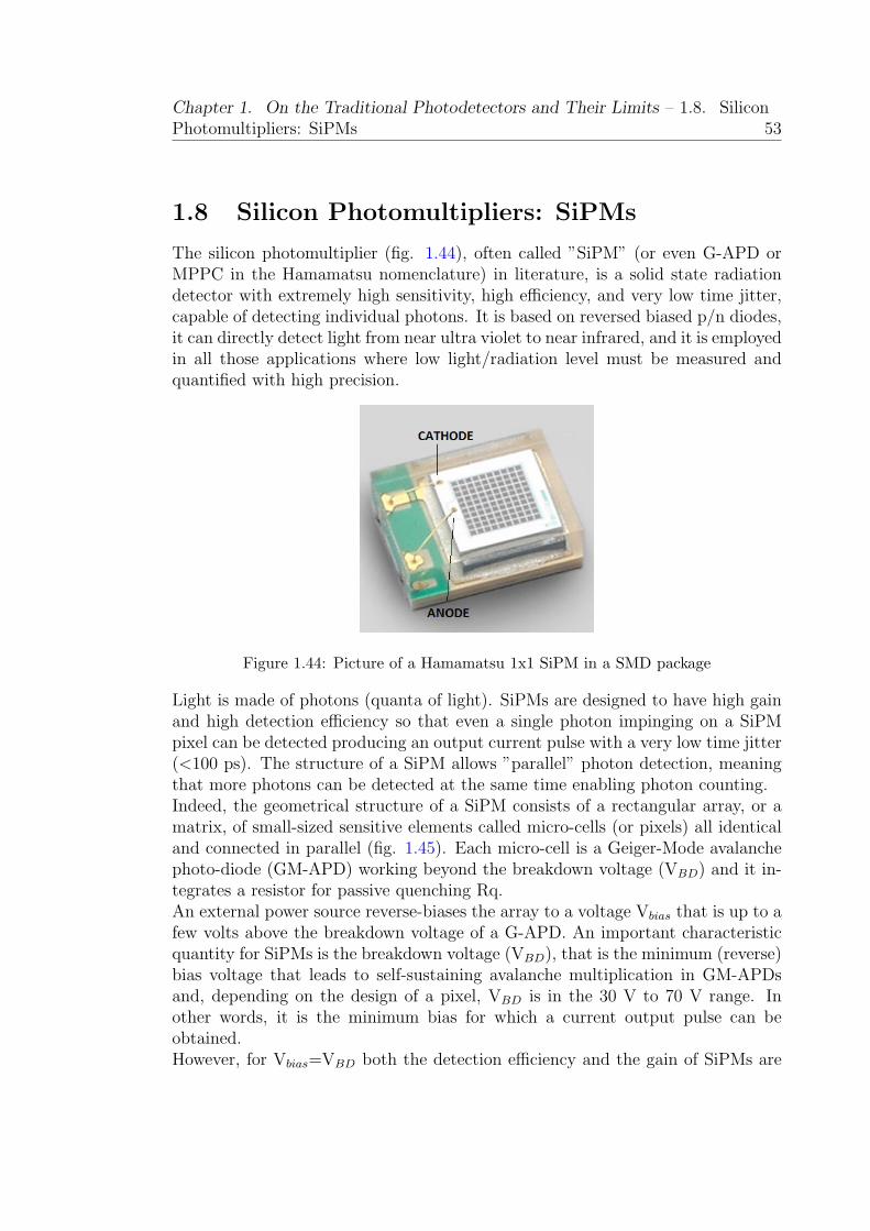
Chapter 1. On the Traditional Photodetectors and Their Limits – 1.8. SiliconPhotomultipliers: SiPMs 53
1.8 Silicon Photomultipliers: SiPMs
The silicon photomultiplier (fig. 1.44), often called ”SiPM” (or even G-APD orMPPC in the Hamamatsu nomenclature) in literature, is a solid state radiationdetector with extremely high sensitivity, high efficiency, and very low time jitter,capable of detecting individual photons. It is based on reversed biased p/n diodes,it can directly detect light from near ultra violet to near infrared, and it is employedin all those applications where low light/radiation level must be measured andquantified with high precision.
Figure 1.44: Picture of a Hamamatsu 1x1 SiPM in a SMD package
Light is made of photons (quanta of light). SiPMs are designed to have high gainand high detection efficiency so that even a single photon impinging on a SiPMpixel can be detected producing an output current pulse with a very low time jitter(<100 ps). The structure of a SiPM allows ”parallel” photon detection, meaningthat more photons can be detected at the same time enabling photon counting.Indeed, the geometrical structure of a SiPM consists of a rectangular array, or amatrix, of small-sized sensitive elements called micro-cells (or pixels) all identicaland connected in parallel (fig. 1.45). Each micro-cell is a Geiger-Mode avalanchephoto-diode (GM-APD) working beyond the breakdown voltage (VBD) and it in-tegrates a resistor for passive quenching Rq.An external power source reverse-biases the array to a voltage Vbias that is up to afew volts above the breakdown voltage of a G-APD. An important characteristicquantity for SiPMs is the breakdown voltage (VBD), that is the minimum (reverse)bias voltage that leads to self-sustaining avalanche multiplication in GM-APDsand, depending on the design of a pixel, VBD is in the 30 V to 70 V range. Inother words, it is the minimum bias for which a current output pulse can beobtained.However, for Vbias=VBD both the detection efficiency and the gain of SiPMs are

Chapter 1. On the Traditional Photodetectors and Their Limits – 1.8. SiliconPhotomultipliers: SiPMs 54
Figure 1.45: Detail of the matrix of microcells and schematic of the parallel arrangement
of GM-APDs with series quenching resistor in a SiPM
(by definition) still null as we will see later. Only for Vbias > VBD output currentpulses are actually observed. The difference between Vbias and VBD is commonlyreferred to as overvoltage (VOV ), which is one of the most important operationalparameters of an SiPM. By definition:
VOV = Vbias − VBD. (1.66)
In principle, the higher the overvoltage, the higher the SiPM performances. Inreality, since the detection efficiency tends to saturate with VOV while the noisekeeps on increasing (even more than linearly) with VOV , there exist an upper limitto the optimum SiPM bias voltage.
1.8.1 SiPM’s Architecture
Figure 1.46 illustrate a common architecture of a G-APD array. The accompanyingfigure 1.47 shows schematically the distribution of the dopant ions or space charge

Chapter 1. On the Traditional Photodetectors and Their Limits – 1.8. SiliconPhotomultipliers: SiPMs 55
Figure 1.46: Architecture of a silicon photomultiplier (side view). The depicted structure
of a single pixel is known as ”reach-through” structure, popular with manufacturers
(left panel) and the resulting strength of the electric field (right panel) as a functionof depth.
Figure 1.47: Schematic distribution of dopant ions (left) and the resulting electric field
(right) for a pixel in the structure shown above
Following the direction of light (red arrows in the leftmost pixel of figure 1.46) theyfirst encountered a very thin (typ. ∼10 nm) anti-reflection coating. The coatingimproves light transmittance to the next layer, a transparent silicon dioxide (SiO2),which acts as the window and an insulation between the metal contacts above andsemiconductor below. A typical thickness of the insulation is ∼0.15 µm. Furtherbelow, there is a heavily doped n+ layer, which is connected to the metal contactabove through the quenching resistor Rq (made of polysilicon). The thickness
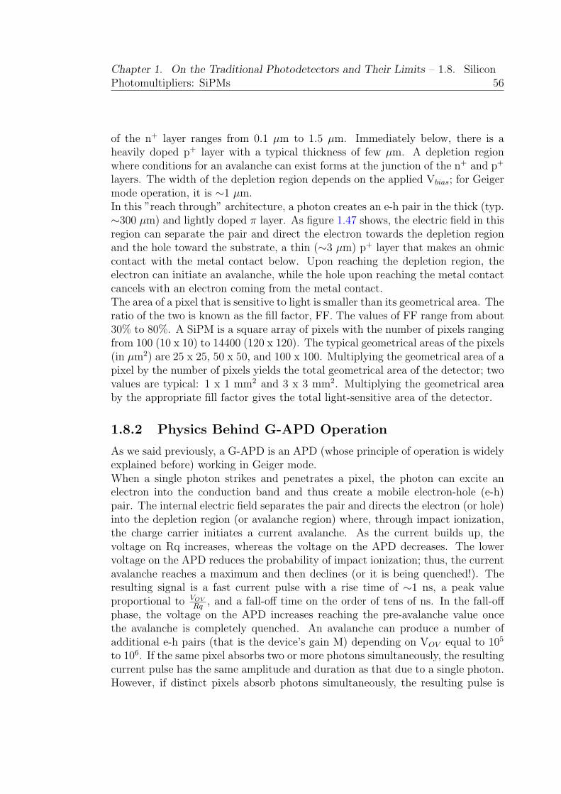
Chapter 1. On the Traditional Photodetectors and Their Limits – 1.8. SiliconPhotomultipliers: SiPMs 56
of the n+ layer ranges from 0.1 µm to 1.5 µm. Immediately below, there is aheavily doped p+ layer with a typical thickness of few µm. A depletion regionwhere conditions for an avalanche can exist forms at the junction of the n+ and p+
layers. The width of the depletion region depends on the applied Vbias; for Geigermode operation, it is ∼1 µm.In this ”reach through” architecture, a photon creates an e-h pair in the thick (typ.∼300 µm) and lightly doped π layer. As figure 1.47 shows, the electric field in thisregion can separate the pair and direct the electron towards the depletion regionand the hole toward the substrate, a thin (∼3 µm) p+ layer that makes an ohmiccontact with the metal contact below. Upon reaching the depletion region, theelectron can initiate an avalanche, while the hole upon reaching the metal contactcancels with an electron coming from the metal contact.The area of a pixel that is sensitive to light is smaller than its geometrical area. Theratio of the two is known as the fill factor, FF. The values of FF range from about30% to 80%. A SiPM is a square array of pixels with the number of pixels rangingfrom 100 (10 x 10) to 14400 (120 x 120). The typical geometrical areas of the pixels(in µm2) are 25 x 25, 50 x 50, and 100 x 100. Multiplying the geometrical area of apixel by the number of pixels yields the total geometrical area of the detector; twovalues are typical: 1 x 1 mm2 and 3 x 3 mm2. Multiplying the geometrical areaby the appropriate fill factor gives the total light-sensitive area of the detector.
1.8.2 Physics Behind G-APD Operation
As we said previously, a G-APD is an APD (whose principle of operation is widelyexplained before) working in Geiger mode.When a single photon strikes and penetrates a pixel, the photon can excite anelectron into the conduction band and thus create a mobile electron-hole (e-h)pair. The internal electric field separates the pair and directs the electron (or hole)into the depletion region (or avalanche region) where, through impact ionization,the charge carrier initiates a current avalanche. As the current builds up, thevoltage on Rq increases, whereas the voltage on the APD decreases. The lowervoltage on the APD reduces the probability of impact ionization; thus, the currentavalanche reaches a maximum and then declines (or it is being quenched!). Theresulting signal is a fast current pulse with a rise time of ∼1 ns, a peak valueproportional to VOV
Rq, and a fall-off time on the order of tens of ns. In the fall-off
phase, the voltage on the APD increases reaching the pre-avalanche value oncethe avalanche is completely quenched. An avalanche can produce a number ofadditional e-h pairs (that is the device’s gain M) depending on VOV equal to 105
to 106. If the same pixel absorbs two or more photons simultaneously, the resultingcurrent pulse has the same amplitude and duration as that due to a single photon.However, if distinct pixels absorb photons simultaneously, the resulting pulse is

Chapter 1. On the Traditional Photodetectors and Their Limits – 1.8. SiliconPhotomultipliers: SiPMs 57
a superposition of the single-photon pulses; its amplitude is proportional to thenumber of independently ”fired” pixels.The main difference between APDs and G-APDs is the fact that the output signalof a G-APD is not proportional to the amount of input light. Indeed we are inthe third region of figure 1.42, where the avalanche caused by injection of a singlecharge carrier does not stop, it is self-sustained. As a result, a current flows throughthe G-APD and its value depends on the overvoltage, VOV . The steepness of thecurve in this region implies that the magnitude of the current is very sensitive toVOV . The strong electric field in the avalanche region maintains e-h plasma whereboth electrons and holes comparably ionize the lattice atoms (i.e. α ∼ β). In asteady state, the number of newly created pairs is equal to the number of pairscollected at the electrodes. If it is desired to extinguish the avalanche, Vbias mustbe reduced to at least VBD; doing so ”quenches” the avalanche.
1.8.3 Operation Principles
The operation principle of a SiPM can be modeled by means of the equivalentcircuit of a GM-APD (shown in fig. 1.48).
Figure 1.48: The equivalent circuit of a GM-APD with series quenching resistor and
external bias. The region of the circuit delineated by the dashed rectangle represents
an APD operating in Geiger mode. The switch is in the OFF position when the APD
is in the ”ready” state, while it goes to the ON state the instant a charge initiates
an avalanche. So the switch models the turn-on (photon absorptionor dark event) and
turn-off (quenching) probabilities
Cd (typ. ∼ 0.1pF ) is the junction capacitance in reverse bias, Rs (typ. ∼ 1kΩ)models the equivalent RC circuit resistance that takes account of the characteristictime needed for the signal creation, Rq (typ. ∼ 150kΩ) is the quenching resistor
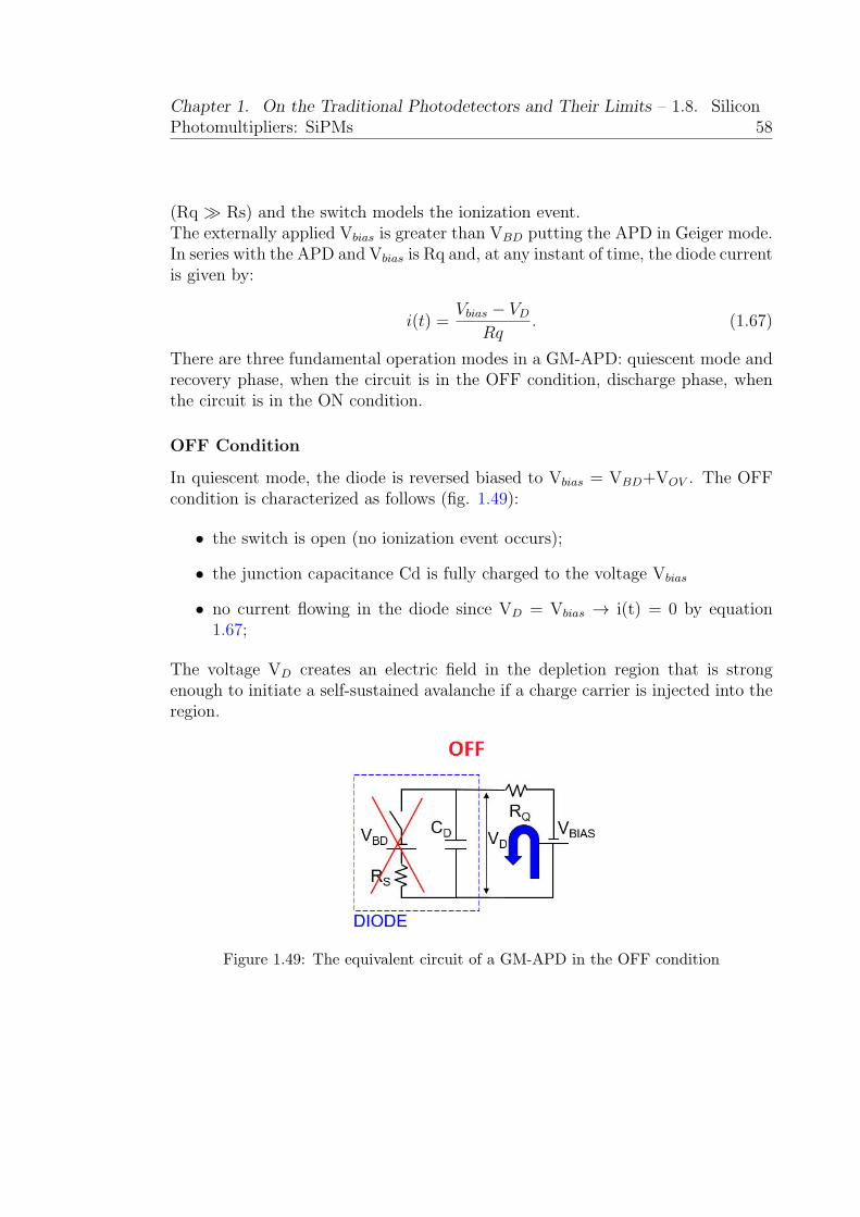
Chapter 1. On the Traditional Photodetectors and Their Limits – 1.8. SiliconPhotomultipliers: SiPMs 58
(Rq ≫ Rs) and the switch models the ionization event.The externally applied Vbias is greater than VBD putting the APD in Geiger mode.In series with the APD and Vbias is Rq and, at any instant of time, the diode currentis given by:
i(t) =Vbias − VD
Rq. (1.67)
There are three fundamental operation modes in a GM-APD: quiescent mode andrecovery phase, when the circuit is in the OFF condition, discharge phase, whenthe circuit is in the ON condition.
OFF Condition
In quiescent mode, the diode is reversed biased to Vbias = VBD+VOV . The OFFcondition is characterized as follows (fig. 1.49):
• the switch is open (no ionization event occurs);
• the junction capacitance Cd is fully charged to the voltage Vbias
• no current flowing in the diode since VD = Vbias → i(t) = 0 by equation1.67;
The voltage VD creates an electric field in the depletion region that is strongenough to initiate a self-sustained avalanche if a charge carrier is injected into theregion.
Figure 1.49: The equivalent circuit of a GM-APD in the OFF condition

Chapter 1. On the Traditional Photodetectors and Their Limits – 1.8. SiliconPhotomultipliers: SiPMs 59
ON Condition
In the discharge phase the ionization occurs at the time ti. The ON condition ischaracterized as follows (fig. 1.50):
• the switch is closed;
• Cd discharges to VBD through the fictive resistor Rs, between ti and tmax,with the characteristic time constant τ ∼ Rs · Cd (typ. ∼ 100ps);
• the diode current grows to:
IMAX =Vbias − VBD
Rq +Rs. (1.68)
Figure 1.50: The equivalent circuit of a GM-APD in the ON condition
OFF Condition Again
The voltage VD during the discharge decreases and approaches an asymptoticvalue given by the following equation20:
VD = Vbias −Rq(Vbias − VBD)
Rq +Rs= Vbias −
VOV
1 + RsRq
. (1.69)
As VD decreases, the electric field in the depletion region becomes too weak tomaintain Geiger mode and the self-sustained avalanche it’s been quenched. Thisis the recovery phase characterized as follows:
• the switch goes open;
20Since Rq ≫ Rs, the equation shows that VD tends to VBD

Chapter 1. On the Traditional Photodetectors and Their Limits – 1.8. SiliconPhotomultipliers: SiPMs 60
• Cd recharges from VBD to Vbias through Rq, for times greater than tmax,with the characteristic time constant τ ∼ Rq · Cd (typ. ∼ 15 ns);
• the diode current decreases to ∼ 0 A.
At the end of the charging process, the APD is in the ”ready” state again.Because Rs ·Cd ≪ Rq ·Cd, the current rises more steeply before tmax then it fallsoff after tmax. Thus, the output current pulse has the characteristic asymmetricshape depicted in figure 1.51.
Figure 1.51: Current pulse produced by a micro-cell in response to photon absorption
(single-cell signal), its amplitude is defined to be 1 p.e.
An integral of i(t) with respect to time from ti to infinity is the area under thiscurve, which equals the net charge Q produced in the avalanche. A detailedanalysis yields the following:
Q = Cd · (Vbias − VBD). (1.70)
Since the charge Q is due to a single charge injected into the avalanche region, thegain M for this process can be defined by the following equation:
M ≡ Q
e. (1.71)
For a fully-depleted junction, Cd is constant with respect to the applied voltageand, thus, equation above shows that M is linearly proportional to Vbias − VBD =VOV . The typical values of M range from 105 to 106. If more than one pixeldeveloped an avalanche at the time ti, the total charge generated by an SiPM isthe following:
Qout = Nf ·Q = Nf · Cd · (Vbias − VBD). (1.72)

Chapter 1. On the Traditional Photodetectors and Their Limits – 1.8. SiliconPhotomultipliers: SiPMs 61
Figure 1.52: Waveforms for Hamamatsu S13360-4929 SiPM producing signal when 1,
2, 3, ... pixels fired simultaneously in response to low incoming light. The waveforms
are for gain M = 1.8 x 10⁶ and 20x linear amplifier, acquired with the Teledine LeCroy
serial data analyzer mod. SDA 760Zi-A
Here, Nf is the number of pixels that nearly simultaneously ”fired” or developedavalanches.Figure 1.52 shows oscilloscope traces of waveforms produced by a SiPM in responseto low-intensity light (∼ 40 incident photons). From bottom up, the waveformscorrespond to the outputs characterized by an increasing number of simultane-ously ”fired” independent pixels. The waveforms labeled 1 p.e. are for the outputswhere only one pixel has fired in response to light. Note that if two or more pho-tons were to be simultaneously absorbed by this same pixel, the output waveformwould have been the same. Similarly, the waveforms labeled 2 p.e. are for twopixels firing simultaneously and so on. To obtain these cumulative waveforms, theoscilloscope is set to the persistence mode; thus, the color in the figure (from redto violet) corresponds to the frequency with which the events have occurred (fromthe most common to the rarest). There is a clear demarcation between waveformslabeled 1 p.e., 2 p.e., 3 p.e., etc. The 4 and 5 p.e. waveforms are linked to eventsthat occur more frequently (red color), whereas the other events gradually becomeless frequent. Note that there are a few 1 and 2 p.e. waveforms that are laggingin time to the main events. They can be generated in three ways: dark noise,afterpulsing, and cross-talk.Dark noise pulses occur randomly and are due to thermally-generated charge car-riers reaching the avalanche region. If a pixel is in the ”ready” state, the ensuing”dark” pulse is indistinguishable from one due to photon absorption. Such a pulse
Chapter 1. On the Traditional Photodetectors and Their Limits – 1.8. SiliconPhotomultipliers: SiPMs 62
would be labeled 1 p.e. in figure 1.52. If, however, the pixel is recovering from aprimary avalanche, the ”dark” pulse lags in time to the primary pulse but is notcorrelated with it.The pulses due to afterpulsing and cross-talk are correlated to the primary avalanche,which can be due to photon absorption or dark noise. Afterpulsing occurs whenlattice defects trap charge during an avalanche and then release the charge whilethe pixel recovers. The release triggers a correlated secondary avalanche whosegain M depends on VOV at the time of release. Cross-talk occurs whe, during aprimary avalanche in a pixel, electron-hole recombinations produce UV photons.If the same pixel reabsorbs the photon, the resulting secondary pulse would looklike an afterpulse. However, if a nearby pixel absorbs the photon, the secondarycorrelated avalanche may be close enough in time to the primary that the result-ing waveform would be labeled 2 p.e. in figure 1.52. The next section discusses ingreater detail dark noise, afterpulsing, and cross-talk.Beyond the single photon resolution, other advantages of G-APDs are summarizedbelow:
• Work at low bias voltage (∼ 50÷ 70 V);
• Have low power cosumption(
< 50 µW
mm2
)
;
• Are insensitive to magnetic fields up to 15 T;
• Are compact and rugged;
• Have a small sensitivity to charged particles traversing the device because ofthe very thin thickness of the silicon wafer (small nuclear counter effect);
• Tolerate accidental illumination;
• Have long lifetime.
So, because of its high internal gain and the additional features summarized above,SiPMs are the preferred alternatives to PMTs. Despite their many advantages theyhave also some drawbacks:
• The dark noise, that cannot be discriminated from the signal;
• Gain depends on temperature, since the breakdown voltage changes as afunction of temperature;
• The size21, that is limited by the dark noise. The thermal noise increases asthe area increases, a good compromise between size and dark noise shouldbe taken to obtain a device with reasonably good detection characteristics.
21SiPMs sizes can range between 1 mm2 up to 16 mm2
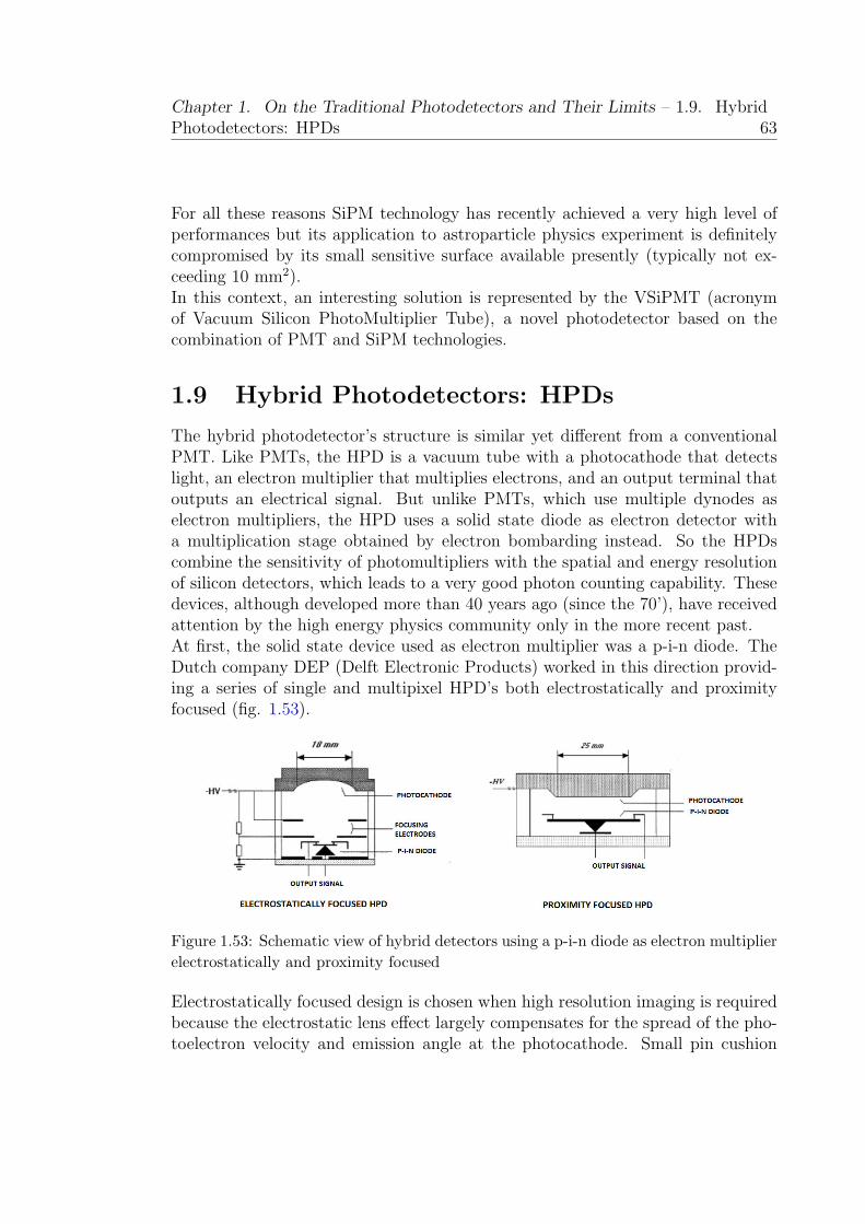
Chapter 1. On the Traditional Photodetectors and Their Limits – 1.9. HybridPhotodetectors: HPDs 63
For all these reasons SiPM technology has recently achieved a very high level ofperformances but its application to astroparticle physics experiment is definitelycompromised by its small sensitive surface available presently (typically not ex-ceeding 10 mm2).In this context, an interesting solution is represented by the VSiPMT (acronymof Vacuum Silicon PhotoMultiplier Tube), a novel photodetector based on thecombination of PMT and SiPM technologies.
1.9 Hybrid Photodetectors: HPDs
The hybrid photodetector’s structure is similar yet different from a conventionalPMT. Like PMTs, the HPD is a vacuum tube with a photocathode that detectslight, an electron multiplier that multiplies electrons, and an output terminal thatoutputs an electrical signal. But unlike PMTs, which use multiple dynodes aselectron multipliers, the HPD uses a solid state diode as electron detector witha multiplication stage obtained by electron bombarding instead. So the HPDscombine the sensitivity of photomultipliers with the spatial and energy resolutionof silicon detectors, which leads to a very good photon counting capability. Thesedevices, although developed more than 40 years ago (since the 70’), have receivedattention by the high energy physics community only in the more recent past.At first, the solid state device used as electron multiplier was a p-i-n diode. TheDutch company DEP (Delft Electronic Products) worked in this direction provid-ing a series of single and multipixel HPD’s both electrostatically and proximityfocused (fig. 1.53).
Figure 1.53: Schematic view of hybrid detectors using a p-i-n diode as electron multiplier
electrostatically and proximity focused
Electrostatically focused design is chosen when high resolution imaging is requiredbecause the electrostatic lens effect largely compensates for the spread of the pho-toelectron velocity and emission angle at the photocathode. Small pin cushion

Chapter 1. On the Traditional Photodetectors and Their Limits – 1.9. HybridPhotodetectors: HPDs 64
shape distortions at large distance from the optical axis are typical for this design.Proximity focused design leads to compact and, because of the small gap betweenphotocathode and silicon sensor, highly B-field tolerant detectors. Because thereis no demagnification, the photosensitive area of the detector is limited to the sizeof the silicon sensor.These devices were not very successful, mainly because of their poor internal am-plification. Indeed, as can be seen from figure 1.54, to obtain a 3.5 x 10³ gain,15kV power supply voltage is required.
Figure 1.54: Typical HPD gain
Hamamatsu photonics provided an upgrade fabricating a proximity focused HPDequipped with an avalanche diode APD instead of a p-i-n diode (fig.1.55).APDs are high-speed and high sensitivity silicon devices which consist of reversebiased p-n junctions, so the electron multiplication is generated by the avalancheprocess triggered by the arrival of photons on the device’s surface, which generateselectron-hole pairs that, drifting across the depletion region of the silicon bulk,create additional pairs. APDs have a low gain factor (∼ 100) so in this device theelectron multiplication is carried out in two steps (fig. 1.55):
• an electron-bombardment stage, where photoelectrons are accelerated to-wards the APD by a large voltage difference (∼ 8 kV) and simultaneuslyacquire high kinetic energy (gain = 3 x 10³);
• an APD stage (gain = 50 x 100) where, because of the kinetic energy gainedin the previous stage, each photoelectron produces many electron-hole pairstriggering a big avalanche that results in a total gain of about 105.
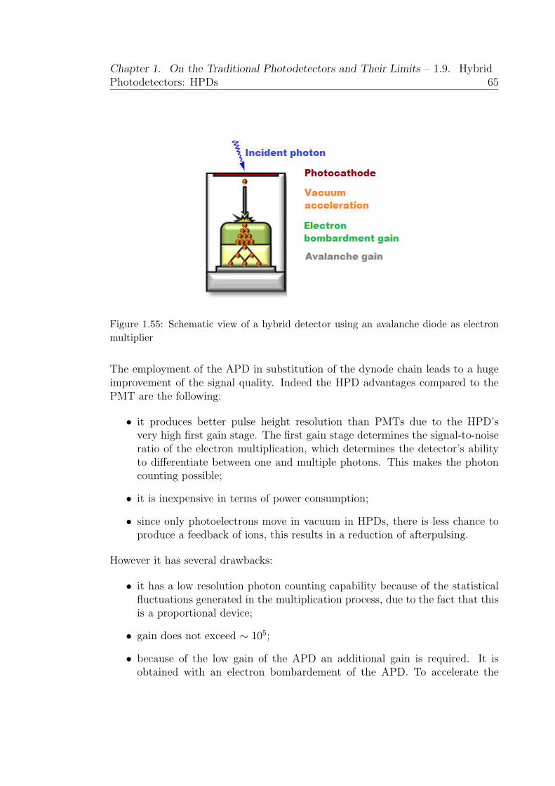
Chapter 1. On the Traditional Photodetectors and Their Limits – 1.9. HybridPhotodetectors: HPDs 65
Figure 1.55: Schematic view of a hybrid detector using an avalanche diode as electron
multiplier
The employment of the APD in substitution of the dynode chain leads to a hugeimprovement of the signal quality. Indeed the HPD advantages compared to thePMT are the following:
• it produces better pulse height resolution than PMTs due to the HPD’svery high first gain stage. The first gain stage determines the signal-to-noiseratio of the electron multiplication, which determines the detector’s abilityto differentiate between one and multiple photons. This makes the photoncounting possible;
• it is inexpensive in terms of power consumption;
• since only photoelectrons move in vacuum in HPDs, there is less chance toproduce a feedback of ions, this results in a reduction of afterpulsing.
However it has several drawbacks:
• it has a low resolution photon counting capability because of the statisticalfluctuations generated in the multiplication process, due to the fact that thisis a proportional device;
• gain does not exceed ∼ 105;
• because of the low gain of the APD an additional gain is required. It isobtained with an electron bombardement of the APD. To accelerate the

Chapter 1. On the Traditional Photodetectors and Their Limits – 1.9. HybridPhotodetectors: HPDs 66
electrons towards the APD a very high voltage has to be supplied to thephotocathode; this makes the gain instable since it depends on the stabilityof the HV;
• isolation is complicated due to its particular manufacturing.
The amplification factor of this detector is ∼ 105, therefore it is much lower thanthat of the PMT (∼ 107). In many applications where high sensitivity is requiredat low light levels, this gain is insufficient, and that’s the reason why PMT’s arestill the preferred device for low light detection.So the innovative idea is to develop a new type of vacuum photomultiplier in whichthe photoelectron multiplication is performed using APDs operating in a high-gainregime in which a reverse bias voltage, above the breakdown voltage, is appliedto the diodes, i.e. the Geiger mode. In this mode of operation the multiplicationfactor of the G-APDs reaches values ∼ 106, and no more electron-bombardmentis needed. This results in a superior gain stability since it depends only on themultiplication device (supplied at 70V) and not on the photocathode (supplied at8kV); moreover, no fluctuations in photon counting occur since G-APDs give aboolean type answer (the photon is passed or not) and not a proportional answer.
Figure 1.56: Evolution of vacuum tube detectors
This idea is, therefore, proposed to return to the concept of the PMT gain (thereis not an intermediate amplification stage between the photocathode and the mul-tiplication element) by exploiting the G-APD technology with its superior per-formances in single photon detection, no fluctuations in the multiplication phase,high gain with no high power supply required (fig. 1.56).

Chapter 2
The Idea Behind VSiPMT
To overcome all the problems listed before, Professor Giancarlo Barbarino from theUniversity of Naples Federico II proposed the VSiPMT (Vacuum Silicon Photo-Multiplier Tube fig. 2.1): an innovative design for a revolutionary photon detectorfor Astroparticle Physics applications.The VSiPMT has many attractive features. In particular, a low power consump-tion and an excellent photon counting capability [20].
Figure 2.1: Schematic view of the VSiPMT
For these reasons, this project, aimed at creating new scientific instrumentationfor future missions of Exploration and Observation of the Universe, was funded bythe Italian Space Agency (ASI) and by the Italian National Institute for NuclearPhysics (INFN). After the feasibility test of the idea, in which the performanceof a special non-windowed SiPM realized by the company Hamamatsu (SiPM)have been tested as electron detector and current amplifier, Hamamatsu realizedalso two VSiPMT industrial prototypes, that have been fully characterized. Theencouraging results of this analysis convinced Hamamtsu Photonics to assemble a
67
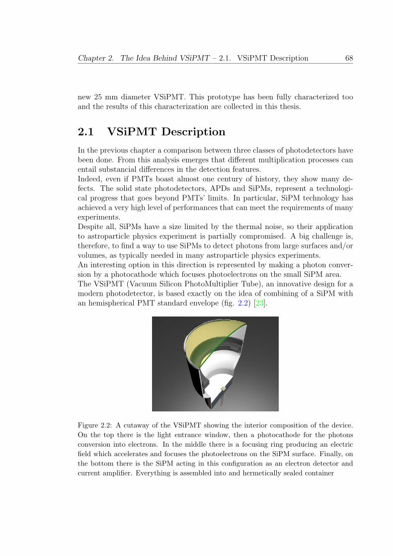
Chapter 2. The Idea Behind VSiPMT – 2.1. VSiPMT Description 68
new 25 mm diameter VSiPMT. This prototype has been fully characterized tooand the results of this characterization are collected in this thesis.
2.1 VSiPMT Description
In the previous chapter a comparison between three classes of photodetectors havebeen done. From this analysis emerges that different multiplication processes canentail substancial differences in the detection features.Indeed, even if PMTs boast almost one century of history, they show many de-fects. The solid state photodetectors, APDs and SiPMs, represent a technologi-cal progress that goes beyond PMTs’ limits. In particular, SiPM technology hasachieved a very high level of performances that can meet the requirements of manyexperiments.Despite all, SiPMs have a size limited by the thermal noise, so their applicationto astroparticle physics experiment is partially compromised. A big challenge is,therefore, to find a way to use SiPMs to detect photons from large surfaces and/orvolumes, as typically needed in many astroparticle physics experiments.An interesting option in this direction is represented by making a photon conver-sion by a photocathode which focuses photoelectrons on the small SiPM area.The VSiPMT (Vacuum Silicon PhotoMultiplier Tube), an innovative design for amodern photodetector, is based exactly on the idea of combining of a SiPM withan hemispherical PMT standard envelope (fig. 2.2) [23].
Figure 2.2: A cutaway of the VSiPMT showing the interior composition of the device.
On the top there is the light entrance window, then a photocathode for the photons
conversion into electrons. In the middle there is a focusing ring producing an electric
field which accelerates and focuses the photoelectrons on the SiPM surface. Finally, on
the bottom there is the SiPM acting in this configuration as an electron detector and
current amplifier. Everything is assembled into and hermetically sealed container

Chapter 2. The Idea Behind VSiPMT – 2.2. Photocathodes 69
The idea was born in Naples in 2007 with the goal to enlarge indirectly the SiPMsensitive surface, thus exploiting its good detection features also in large astropar-ticle physics experiments [24]. In this device the multiplication stage is providedby the SiPM that acts as electron detector and so as current amplifier.
2.2 Photocathodes
The VSiPMT design includes a photocathode to convert photons into electronsthat will be than detected and thus multiplied by the SiPM.Photocathodes are mostly made of compound semiconductors, consisting of alkalimetals with a low work function1, and can be operated both in reflection (opaque)and in transmission mode (semitransparent) [25]. In the former case, when thelight enters and impinges on the photocathode a photoelectron is extracted in thesame side of the incoming light and is driven on the multiplying sensor (fig. 2.3right), while in the latter case when the light impinges on the photocathode aphotoelectron is extracted on the opposite side with respect to the incoming light(fig. 2.3 left).
Figure 2.3: Reflective and transmission mode photocathodes operating principle
In both configurations, different materials can be used. The materials can be cho-sen depending on the spectral region of sensitivity and on the achievable quantumefficiency.
1In solid-state physics, the work function is the minimum thermodynamic work (i.e. energy)needed to remove an electron from a solid to a point in the vacuum immediately outside thesolid surface.

Chapter 2. The Idea Behind VSiPMT – 2.2. Photocathodes 70
The spectral response of several materials is showed in figure 2.4. Photocathodesoperation can be described using the energy band theory expressed in terms of theenergy gap (EG), electron affinity (EA), Fermi level (EF ), work function (φ), andso on.
Figure 2.4: Spectral response of photoelectron emissive materials
When a photon strikes a photocathode, electrons in the valence band absorb pho-ton energy (Eγ) and become excited to the conduction band, diffusing toward thephotocathode surface.If the energy of these electrons overcomes the vacuum barrier, then they are emit-ted into the vacuum. This electron emission process was expressed as follows byW. E. Spicer [26] by means of his three step model, which explains the photo-electron emission process using three steps: optical absorption process, electrondiffusion process, and escape process [27]:
η = (1−R) · αPE
α· 1
1 + 1
αL
· PS (2.1)
Where η is the conversion efficiency of the photocathode material (i.e. quantumefficiency, function of the photon frequency), R is the reflection coefficient, α isthe full optical absorption coefficient for photons, αPE is the absorption coefficientwhen electrons are excited to a level greater than the vacuum level, L is thediffusion lenght of electrons, PS is the escape probability of electrons.It is clear, from this expression that it is possible to enhance the quantum efficiencyby extending the diffusion length L to improve the crystalline properties of thephotocathodes and also reduce the electron affinity by increasing the PS (NEA-photocathodes).

Chapter 2. The Idea Behind VSiPMT – 2.2. Photocathodes 71
It has been studied that a crystalline photocathode when activated by depositinga few monolayers of cesium and a strong oxidizer (such as fluorine or oxygen)gain the NEA (Negative Electron Affinity) property. This means that the Cs-Oactivation causes the energy band in the surface to curve downward so that theelectron affinity has a negative value, thus allowing electrons at the bottom of theconduction band to escape (fig. 2.5).
Figure 2.5: NEA photocathode band model
The most used photocathode materials are:
• CsI: cesium iodide is not sensitive to solar radiation and therefore oftencalled ”solar blind”. Its sensitivity sharply falls off at wavelengths longer than200 nanometers and it is exclusively used for vacuum ultraviolet detection.
• Bialkali (Sb-Rb-Cs, Sb-K-Cs): Since two kinds of alkali metals are em-ployed, these photocathodes are called ”bialkali”. The transmission type ofthese photocathodes has a spectral response ranging between ultraviolet andvisible region. On the other hand, the reflection-type bialkali photocathodesare fabricated by using the same materials, but different processing. As aresult, they offer enhanced sensitivity on the long wavelength side, achievinga spectral response from the ultraviolet region to around 700 nanometers.
• Multialkali (Sb-Na-K-Cs): This photocathode uses three or more kindsof alkali metals. Due to high sensitivity over a wide spectral response rangefrom the ultraviolet through near infrared region around 850 nm.
• Ag-O-Cs: Transmission type photocathodes using this material are sensitivefrom the visible through near infrared region, from 400 to 1200 nm, while

Chapter 2. The Idea Behind VSiPMT – 2.3. Entrance Window 72
the reflection type exhibits a slightly narrower spectral response region from300 to 1100 nm. Ag-O-Cs photocathodes are chiefly used for near infrareddetection.
2.3 Entrance Window
Each entrance window material transmit the incoming light in a different waydepending on the wavelength. In particular, these materials tend to absorb ultra-violet light and, as a consequence, the choise of the window material determinsthe short wavelenght sensitivity limit of the whole device [28].The most used window materials are:
• MgF2: A magnesium fluoride crystal is used as a practical window materialbecause it allows transmission of vacuum ultraviolet radiation down to 115nm.
• Synthetic silica: It transmits ultraviolet radiation down to 160 nm.
• Borosilicate glass: This is the most commonly used window material.The borosilicate glass does not transmit ultraviolet radiation shorter than300 nanometers. It is not suited for ultraviolet detection shorter than thiswavelength.
A plot of the window material transmittance with respect to wavelenghts is infigure 2.6 together with table which summarizes a final overview about how theentrance windows usually matches the photocathodes (fig. 2.7).
Figure 2.6: A plot of the transmittance of several window materials with respect to
wavelenght

Chapter 2. The Idea Behind VSiPMT – 2.4. The SiPM as Electron Multiplier73
Figure 2.7: Reference for spectral response of transmission mode photocathodes
2.4 The SiPM as Electron Multiplier
As said above, the VSiPMT is a new configuration for an hybrid photodetector inwhich the dynode chain is replaced by a SiPM, which acts as electron detectorand multiplier [29].For this purpose a SiPM has to become a SiEM (Silicon Electron Multiplier).Since photoelectrons produced by the photocathode need a certain energy to enterinto the Silicon bulk starting the Geiger avalanche and so to give a signal, highvoltage between photocathode and SiPM is required. A special windowless SiPMis necessary to minimize the threshold energy required. When an electron entersinto the Silicon bulk it generates electron-hole pairs by ionization. In this case theElectron Detection Effciency, namely EDE, can be evaluated as follows:
EDE = FF · (1− η) · (Pe + Ph − Pe · Ph), (2.2)
which says that the probability that an impinging electron is detected depends onthree factors: FF, the fill factor of the SiPM; η the backscattering coefficient; Pe
and Ph are respectively the probability that the geiger avalanche is generated byan electron or a hole.Since the SiPM is a matrix of cells the separation between the cells is a dead area,the percentage of active area of the device is, thus, given by the fill factor, FF, thatrepresents therefore the geometric factor. When an electron impinges the SiPMsurface, the entrance probability scales with the geometric factor FF.An electron hitting the SiPM surface has a probability η to be backscattered.Hence, the probability that an electron enters in the Silicon bulk is (1− η).Finally, once the electron is entered, it produces an ionization track that generateselectron-hole pairs. In such a device both electrons and holes can start the geiger

Chapter 2. The Idea Behind VSiPMT – 2.4. The SiPM as Electron Multiplier74
avalanche. The probability that the geiger avalanche is triggered by an electron,Pe, is double with respect to the probability that the geiger avalanche is triggeredby an hole, Ph. As a consequence in order to maximize the EDE, the SiPM needsa p over n structure. A more clear outline of the situation can be done by lookingat figure 2.8.
Figure 2.8: n-over-p internal structure of the SiPM (left). p-over-n structure of the SiPM
(right)
On the left a scheme of the processes occuring in a n-over-p configuration arepresented, while on the right picture there are those occurring in a p-over-n con-figuration of the SiPM.The main difference between the two internal structures of the SiPM is that in theformer case the incoming electron needs to cross the high field region in order tolet the electron start the geiger avalanche, while in the latter case is not necessary.Actually, in a p-over-n SiPM the photoelectron ionization range lies in the p+
region allowing electrons to cross the whole high-field zone p+n, going to 0 volt-age, and triggering the Geiger avalanche with high efficiency. This configurationis particularly suited for the VSiPMT application because allows to detect alsoelectrons with a shorter range and so with a lower energy.This simplifies far and away the operation of the VSiPMT making possible toachieve a relatively low operating voltage of the photocathode and focus ring (∼3kV ).The reduction of the thickness of the entrance layer of the junction p+nn+, is anabsolutely necessary condition to allow incident photoelectrons to create sufficientelectron-hole pairs to induce the micro-pixel Geiger discharge at a fixed HV, andmaximize the PDE.Using a Silicon photomultiplier allows to reach a very high gain totally providedby the pixels working in geiger mode. This has many advantages:

Chapter 2. The Idea Behind VSiPMT – 2.4. The SiPM as Electron Multiplier75
• Excellent photon counting. The photocathode is only a passive interme-diary. The photons are converted into electrons that are accelerated towardsthe SiPM surface. The electron entering into the Silicon bulk gives a stan-dard output signal. So as for photons, the device shows an exellent resolutionof the single electron allowing an easy photon counting.
• High gain with low voltage. Differently from a classical HPD, in thiscase the high gain is totally realized by the SiPM pixels operating in geigermode. The electron crossing the geiger region gives an output standardsignal with the typical gain of the SiPM ∼ 106. This means that there isno need for an additional gain step provided by high energy photoelectrons.In such a device, indeed, the photoelectrons only need to enter into theSilicon bulk to produce a signal. Therefore it exists a threshold energy forthe photoelectrons that is necessary to drive them in the geiger region of thedevice and is given by the voltage difference between the photocathode andthe SiPM. The average voltage supplied to the photocathode in a VSiPMTis commonly ∼ 3 kV .
• Negligible power consumption. The absence of the dynode chain entailsthat also the voltage divider used to supply voltage to the dynodes is un-necessary. Removing the voltage divider means that in VSiPMT the powerconsumption is linked only to the photocathode and the SiPM. So thanksto this new configuration a substancial reduction in power consumption isachieved, thus resulting now ≤ mW. This is a great deal for such experimentsoperating in hostile environments (i.e. underwater, in ice or in space).
• No gain dependence on the noise. Since the SiPM operates in geigermode, the gain is not anymore limited by the thermal noise, which is totallyindependent.
• High speed. The absence of a dynode chain means that the transit time islower because it involves only the path from the photocathode to the SiPM.Moreover being the voltage difference between photocathode and SiPM muchhigher with respect to the one in a PMT (∼ kV vs ∼ 100V ) means thatin VSiPMT the photoelectrons have a higher energy and so are faster thanin PMTs. As for transit time, the spread in transit time (TTS) is due tothe electron trajectories between the photocathode and the SiPM and so acertain reduction of the VSiPMT TTS with respect to a classical PMT TTSis expected.
• Compactness and simplicity. Using a SiPM allows to obtain a devicevery compact and mechanically simple, having a lower number of connectionwith respect to a PMT.

Chapter 2. The Idea Behind VSiPMT – 2.4. The SiPM as Electron Multiplier76
The various theoretical studies and feasibility tests that led to the design andimplementation of this innovative device are not a subject of this thesis. We havecharacterized the latest industrial prototype manufactured by Hamamatsu.The results of this work are given in the second part of this thesis.

Part II
Measurements and Data Analysis
Chapter 3
Characterization of SiPMs
Since 2006, Hamamatsu Photonics, a Japanese manufacturer of optical sensors(including photomultiplier tubes), electric light sources, and other optical devicesand their applied instruments for scientific, technical and medical use [17], hasbegun production of a series of SiPMs called Multi-Pixel Photon Counters. TheMulti-Pixel Photon Counter is becoming a popular choice of a photodetector inapplication where even single photons must be detected. Understanding how thisdetector operates and how its optical and electrical characteristics change withrespect to the parameters of an experiment is critical for the proper interpretationof scientific data. In this chapter we are going to present the results of measurementperformed on the latest generations of MPPCs produced by Hamamatsu Photonicsin order to determine their basic optical and electrical characteristics.
3.1 Specifications of the Characterized SiPMs
In this section we will review the features of the devices characterized at our homelab. They all are manufactured by Hamamatsu and belong to different technologicgenerations.
3.1.1 The Latest Generation Series: S13360
The S13360 series are SiPMs for precision measurements (such as DNA sequencer,laser microscope and fluorescence measurements) because of their lower afterpulse,crosstalk and dark counts with respect to previous products as we will see later.They have an effective area of 3 x 3 mm2, our sample had a ceramic package andwas a special windowless device manufactured especially for Prof. Barbarino’sgroup.Tables below (fig. 3.1) summarize the specifications and the operating parameters
78

Chapter 3. Characterization of SiPMs – 3.1. Specifications of the CharacterizedSiPMs 79
of this SiPM at 25C.
Figure 3.1: Summary of S13360 SiPM specifications (our sample is evidenced in purple)
In figure 3.4 is shown the dimensional outline of the photodetector (unit: mm).Metal electrodes, made in oxygen-free copper, provide a connection between inter-nal electrodes (anode and cathode) and the external side of the ceramic package.

Chapter 3. Characterization of SiPMs – 3.1. Specifications of the CharacterizedSiPMs 80
Figure 3.2: S13360 dimensional outline
3.1.2 The Relatively New Series: S10943
This is the special windowless version of another series (S10362) manufacturedespecially for Prof. Barbarino’s group so there is not a commercial datasheet whichsummarizes its characteristics. The absence of the protective entrance windoweases the entrance of the photoelectrons into the silicon bulk, indeed these deviceswhere mounted on the very first home made VSiPMT prototype.These SiPMs have an effective area of 3 x 3 mm2 with 50 µm pixel pitch, oursample had a ceramic package, gain equal to M = 1.25 x 10⁶ and dark counts rateDR = 1091 kcps at 25C.
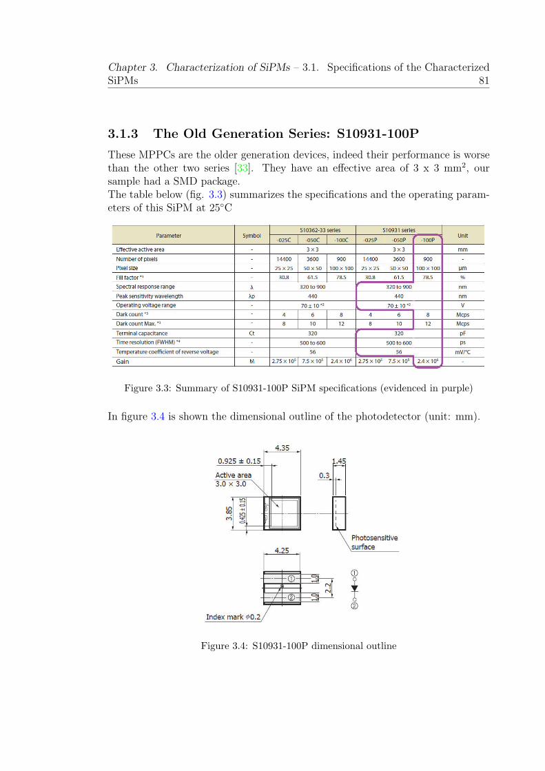
Chapter 3. Characterization of SiPMs – 3.1. Specifications of the CharacterizedSiPMs 81
3.1.3 The Old Generation Series: S10931-100P
These MPPCs are the older generation devices, indeed their performance is worsethan the other two series [33]. They have an effective area of 3 x 3 mm2, oursample had a SMD package.The table below (fig. 3.3) summarizes the specifications and the operating param-eters of this SiPM at 25C
Figure 3.3: Summary of S10931-100P SiPM specifications (evidenced in purple)
In figure 3.4 is shown the dimensional outline of the photodetector (unit: mm).
Figure 3.4: S10931-100P dimensional outline

Chapter 3. Characterization of SiPMs – 3.2. Experimental Set Up andMeasuring Procedure 82
3.2 Experimental Set Up and Measuring Proce-
dure
Every measurement descripted in this chapter was performed between 20 and22C temperature, by means of the following experimental set-up:
• Dark box;
• Digital power meter Newport mod. 815, 1nW sensitivity;
• Hamamatsu Photonics picosecond light pulser (pulse duration = 47 ps) mod.M10306-04, with monochromatic emission in the visible blu/violet light (407nm wavelenght);
• Electronic board made ad hoc for the SiPM’s signal amplification on whichthe SiPM and a current voltage amplifier are mounted;
• DC voltage generator Agilent 0.1V sensitivity mod. E3612A used as a powersupply for the SiPM;
• DC voltage generator Matrix mod. MPS-3005-L-3 used as a dual powersupply for the signal amplifier mounted on the electronic board;
• A Newport optical beam splitter mod. 234607 with 2 outputs:
– A, which outputs 1% of the input optical power;
– B, which outputs 99% of the input optical power;
• A 1 meter ThorLabs 600 µm core multimode optical fiber mod. FT600UMT-0.39NA;
• Variable height support for the fiber optic;
• 3mm Edmundoptics opal diffusing glass;
• Digital Teledine LeCroy serial data analyzer mod. SDA 760Zi-A, 4 inputchannels, 6 GHz bandwidth with 40 GS/s sample rate.
For every measurement we will show the arrangement of this set-up, but the elec-tronic board for SiPM’s signal amplification deserves a separate discussion.SiPMs are current sources with an high nominal internal gain (∼106). Neverthless,depending on the experiment requirements a voltage readout could be preferredwith respect to a current readout. In this situation, a conversion of the SiPMoutput current to a proportional voltage is required. With this aim, a design for

Chapter 3. Characterization of SiPMs – 3.2. Experimental Set Up andMeasuring Procedure 83
a custom amplifier has been studied in order to find the best configuration. It isbased on the current-to-voltage conversion made by an operational amplifier andforsees a current and a voltage feedback op-amp. The general design of this circuitis shown in figure 3.5.
Figure 3.5: General scheme of the amplification circuit
A low noise circuit is necessary to properly analize the device features duringthe characterization phase that will follow. Since op-amps with high bandwidthintegrate a large amount of noise, several op-amps have been considered withdifferent bandwidth and slew rate. The amplified output SiPM signal shape of allthe configurations has been compared and have been observed the electronic noise,the rise time and fall time. From this study emerges that the Texas InstrumentsLMH6624 op-amp is the best solution in terms of noise, timing and gain. It has81dB open loop gain, 95dB common mode rejection ratio, 1.5 GHz gain bandwidthand operates from ± 2.5V to ± 6V in dual mode supply. With this amplificationcircuit, SiPM’s signal’s first peak had an amplitude of ∼ 10mV .
3.2.1 Gain Measurement
The gain (M) is defined as the number of carriers contained in the single-cellcurrent pulse, since this is the number of carriers generated during the avalanche

Chapter 3. Characterization of SiPMs – 3.2. Experimental Set Up andMeasuring Procedure 84
in response to an absorbed photon. From the discussion about the equivalentcircuit model for a GM-APD (fig. 1.48), the gain is given by the discharge of thecapacitor Cd from Vbias = (VBD + VOV ) to VBD and therefore is given by thecharge stored on Cd with a potential difference VOV :
G(VOV ) =Cd · VOV
e(3.1)
where e is the singol electron elementary charge. Assuming Cd constant for Vbias >
VBD, gain increases linearly with the overvoltage.By means of the experimental set-up described at the beginning of this chapterand arranged as in figure 3.6, we performed a gain measurement on the latestgeneration SiPM S13360-4929 produced by Hamamatsu Photonics.
Figure 3.6: Schematic view of our experimental set-up
For this measure we placed the SiPM in very low light conditions. To implementthis condition we had the need to interpose between the head of the laser and theSiPM both the ThorLabs 600 µm core fiber and the beam splitter whose output A(1% of the output power from the red fiber) was sent in input to the SiPM. Withthis set-up, we obtained that the optical power output corresponds to an averageof 10 photons per pulse on the active surface of the detector. This system wascalibrated using the power meter Newport mod. 815.The laser at our disposal was equipped with an output which generates a signalof standard amplitude (2.5V) each time it sends a light pulse. We used this sig-
Chapter 3. Characterization of SiPMs – 3.2. Experimental Set Up andMeasuring Procedure 85
nal as trigger1 for the oscilloscope to acquire the signals produced by the SiPM.Since SiPM’s characteristics vary with the operating voltage (increasing the op-erating voltage improves the photon detection efficiency and time resolution, butalso increases the noise), an optimum operating voltage must be selected to matchthe application; the device’s datasheet provides a recommended operating voltageVOP
2 with which we supplied it.In these conditions, we were able to clearly distinguish the peaks 1, 2, 3 and 4 p.e.Integrating a waveform with respect to time gives the net output charge for theevent. The amount of output charge is linearly proportional to the number of firedpixels, which, in turn, is proportional to the number of simultaneously absorbedphotons. Therefore, this information after integrating each waveform can be ex-pressed in the form of a histogram; figure 3.7 is an example of such a histogrambuilt by means of our oscilloscope3.Assuming that all the SiPM’s pixels are identical, the difference in area between apeak of the spectrum and the following provides a measure of the charge generatedby the individual pixel.By varying the value of the supply voltage Vbias between 54.7 and 55.8 V by 0.1Vsteps, we acquired, for every step, areas of the signals with 10000 measures runs.Then we measured the distances between these peaks (2 p.e. - 1 p.e.), (3 p.e. -2 p.e.), (4 p.e. - 3 p.e.) and, for every value of Vbias we calculated their averagewith their errors.Dividing this by the feedback resistance of the amplifier we get the time integralof the output current generated by the individual SiPM’s pixel, that is its totalcharge. By dividing this total charge by the single electron charge we obtain theSiPM gain M as a function of the supply voltage.
M =1
e
∫
Vmean
Rf
dt =1
e
∫
I1pixeldt =Qtot
e. (3.2)
1Triggering is the means by which we can coax an oscilloscope into showing us what we’relooking for in an input signal, and indeed even simply to display it in a stable fashion. Triggeringtype we used in this thesis is the Edge Trigger
2Typically VOP ∼ VBD + 5V but in this case it was VOP ∼ VBD + 3V3The Teledyne LeCroy SDA 760Zi is provided with a function that allows the user to calculate
automatically the area of a waveform

Chapter 3. Characterization of SiPMs – 3.2. Experimental Set Up andMeasuring Procedure 86
Figure 3.7: SiPM’s output signal and the spectrum of areas beneath the peaks. Notice
that waveforms corresponding to different numbers of fired pixels (and so the peaks in
the spectrum) are extremely well separated
The results of this measurement are shown in figure 3.8 below.As expected, the gain increases linearly with Vbias. On the documentation for thisdevice the nominal gain is specified to be equal to:
M = 1.80 · 106 for Vbias = 54.8V, (3.3)
from the linear regression on the line of best fit:
M = p0 + (Vbias · p1), (3.4)

Chapter 3. Characterization of SiPMs – 3.2. Experimental Set Up andMeasuring Procedure 87
Figure 3.8: Graph of gain versus Vbias for the new generation SiPM S13360-4929
where p0 is the intercept of the line and p1 is its slope, we calculated the gain withits error4:
M = (1.8759976± 0.0397718) · 106 for Vbias = 54.8V, (3.5)
in good agreement with the value provided by the manufacturer.
3.2.2 Dark Counts Rate and Other Noise Sources
Noise in SiPMs is represented by spurious output current pulses produced in ab-sence of light. In silicon, there is a finite probability for carriers (electron and hole)to be generated by thermal agitation. During the quiescent mode, if an electron orhole originates inside the active region of a GM-APD an avalanche is initiated andan output pulse is observed. This is called a ”dark event”. The number of darkevents per unit time is the dark count rate (DCR). In silicon photomultipliers,the thermal generation of carriers doubles approximately every 10C, and so doesthe DCR. Moreover, the DCR scales according to the SiPM area, it is an increasingfunction of the overvoltage, depends on the pixel’s size and even on the quality of
4The following formula has been used for errors propagation: ∆f =
√
∑
(
δfδxi
·∆xi
)2
, where
f is a funcion of n variables f = f(x1, x2...xn) and ∆xi is the uncertainty on the i-th variable

Chapter 3. Characterization of SiPMs – 3.2. Experimental Set Up andMeasuring Procedure 88
the semiconductor wafer.In a single GM-APD a dark event is indistinguishable from a photo-generated one.In both cases, the output pulse has 1 p.e. amplitude. In a SiPM, dark events stillhave 1 p.e. amplitude (neglecting direct optical crosstalk events, discussed below)while the useful signal may consists of more photons impinging on the detector atthe same time producing signals with amplitude greater than 1 p.e. In this case,a threshold can be set to, e.g., 1.5 p.e. to discard the dark events.Besides this primary noise, in SiPMs there are other two sources of noise, i.e., af-terpulsing (AP) and optical crosstalk (OC). Both AP and OC events originatefrom an existing current pulse (which can be either a photonevent or a dark-event)and for this reasons they are referred as to ”correlated noise”. The probability ofhaving an AP or OC event strongly depends on the current density in the originalavalanche and on the triggering probability. Large micro-cells have large gain,hence a high number of carriers flowing during the avalanche and thus high APand OC probability. To contain the correlated noise it is essential to implementSiPMs with small micro-cells [30].Afterpulsing is due to the carriers trapped in silicon defects during the avalanchemultiplication that are released later on during the recharge phase of the GM-APD.It occurs when a secondary avalanche forms in a pixel that is recovering from aphoton- or dark-noise-induced primary avalanche. So this secondary avalancheoccurs some time tA after the primary avalanche starts.The net effect is that we observed a new current pulse on the tail of the originalcurrent pulse (fig. 3.9). AP probability increases more than linearly with the over-voltage and quadratically with the cell size because of the corresponding increasein the gain.The amount of charge generated in an afterpulse is proportional to the area underthe secondary waveform (i.e. the afterpulse itself) with respect to the primarywaveform. The amount of charge increases with tA, and for sufficiently long tAwhen the pixel completely recovers, the afterpulse waveform becomes indistinguish-able from the 1 p.e. waveform. In this case, afterpulsing erroneously increases thenumber of 1 p.e. events in photon counting, which translates into an erroneousincrease in Photon Detection Efficiency (PDE; described in greater detail below).Afterpulsing also increases the recovery time of the fired pixel, which degrades thetime resolution characteristic of an SiPM.The likelihood of afterpulsing increases with increasing VOV because the strongerelectric field in the avalanche region more effectively dislodges the trapped chargesand also increases avalanche probability.

Chapter 3. Characterization of SiPMs – 3.2. Experimental Set Up andMeasuring Procedure 89
Figure 3.9: Example of afterpulse on the signal produce by the Hamamatsu SiPM
S13360-4929-A00013 at its VOP = 54.8V. Printscreen from the Lecroy Wave Runner
104 MXi 1GHz Oscilloscope
Optical crosstalk (fig. 3.10) involves photons emitted during avalanche multiplica-tion and that are re-absorbed in neighboring cells or even in the inactive region ofthe same cell and causing additional current pulses. Three distinct processes forlight emission contribute to the observed crosstalk. Indirect interband recombina-tion between electrons and holes in strong electric fields is primarily responsiblefor the emission of photons with energy below ∼2 eV. Bremsstrahlung radiationdue to scattering of conduction electrons from positive ions is mainly responsiblefor emission of photons of energy between ∼2 eV and ∼2.3 eV. Interband recombi-nation between hot5 conduction electrons and holes is responsible for the emissionof radiation above 2.3 eV [37].Direct OC occurs when an emitted photon reaches the active region of another celltriggering an additional avalanche practically at the same instant of the originalavalanche (consider the speed of light in silicon and the very rapid avalancheignition in GM-APDs).
5Hot carrier injection (HCI) is a phenomenon in solid-state electronic devices where an electronor a hole gains sufficient kinetic energy to overcome a potential barrier necessary to break aninterface state. The term ”hot” refers to the effective temperature used to model carrier density,not to the overall temperature of the device

Chapter 3. Characterization of SiPMs – 3.2. Experimental Set Up andMeasuring Procedure 90
Figure 3.10: The mechanism of cross-talk. An avalanche in the central pixel produces
photons energetic enough so that a correlated avalanche in a neighboring pixel can occur
as a result of the photon absorption
The result is the multiple pulse in figure 3.11. Delayed-OC involves, instead,photons that are re- absorbed in the inactive regions of the SiPM.
Figure 3.11: Example of the combination of afterpulse with optical crosstalk on the signal
produce by the Hamamatsu SiPM S13360-4929-A00013 at its VOP = 54.8V. Printscreen
from the Lecroy Wave Runner 104 MXi 1GHz Oscilloscope

Chapter 3. Characterization of SiPMs – 3.2. Experimental Set Up andMeasuring Procedure 91
The generated electron (or hole) must then diffuse to the active region of a cellbefore being able to trigger an avalanche. The correlated pulse has therefore acertain time-delay (in the order of few ns) with respect to the original one.Since the emission of photons is isotropic, this event has a small probability. More-over, some fraction of the photons will be absorbed in the pixel from which theywere emitted, possibly causing afterpulsing in the pixel. The time for a photon tocross a pixel of size d is
tc ∼ n · dc
, (3.6)
where n is the index of refraction of the material. For silicon n = 3.96; thus, for d= 25 µm, tc = 0.33 ps. This crossing time is much shorter than pixel recovery time(typ. ∼15 ns) and, therefore, the SiPM would output at least a 2 p.e. waveformin response to a single external photon. The value of tc scales linearly with d,but even for a 100 µm pixel, it is still small compared to pixel recovery time.Nevertheless, the probability of cross-talk decreases with pixel size because theemitted photon has an increasing chance of being reabsorbed in the same pixel.As for AP, in first approximation OP probability increases more than linearlywith the overvoltage and quadratically with the cell size. The effect of both APand OC is to produce additional charge with respect to the charge associatedto an original SiPM pulse (photon-event or a dark-event). Recent technologicalinnovations enabled us to drastically reduce the crosstalk, by means of the inclusionof optical insulation structures between one cell and the other (fig. 3.12).
Figure 3.12: Optical insulation structure between cell 1 and cell 2. The secondary
emission photon produced in cell 1 is reflected back in the cell 1
We measured the dark counts rate of the two SiPMs S10943-3360 and S13360-4929as a function of the supply voltage in order to obtain a complete characterizationof them both. The results of these measurement have then been compared.

Chapter 3. Characterization of SiPMs – 3.2. Experimental Set Up andMeasuring Procedure 92
The experimental set-up is the same shown in figure 3.6 keeping the laser off, sothe SiPM was in dark. Then we sent the output signal to the oscilloscope andset the trigger on the signal itself. Our oscilloscope is equipped with a functionthat measures the elapsed time between a trigger event and the next (δtrig), anda feature called ”Trigger Holdoff” that lets the user ignore n trigger events, withn set as desired, and stabilize the display as though there were only one triggerevent per acquisition. By fixing n and measuring the δtrig between the event 0and the event n, the event rate R is obviously given by:
R =Holdoff
δtrig. (3.7)
We set the holdoff so that the elapsed time between a trigger event and the nextwas always ∼100 ms and then we varied the supply voltage between 66.7V and68.1V for S10943-3360 SiPM and between 54.4V and 56.8V for S13360-4929 SiPMin steps of 0.1V; for each step we acquired 1000 measures for δtrig and calculatedtheir mean and standard deviation. For each Vbias we performed measures setting3 different trigger tresholds: 0.5 p.e., 1.5 p.e. and 2.5 p.e.; the results of thesemeasurements are shown in figure 3.13.
Figure 3.13: Comparison between S10943-3360 (left, old generation SiPM) and S13360-
4929 (right, new generation SiPM) dark noise rate as a function of the overvoltage

Chapter 3. Characterization of SiPMs – 3.2. Experimental Set Up andMeasuring Procedure 93
Measurements performed at 0.5 p.e. threshold provide an estimate of the totalnoise rate, inclusive of dark counts and thermal crosstalk events.Measurements performed at 1.5 p.e. treshold and low Vbias should provide anestimate of the rate of events due to cross talk only. This is because at 22C tem-perature the probability that two pixels simultaneously generate a pair for thermalagitation should be low; and even if that happens, for small VOV , the probabil-ity that both the electrons produced are able to trigger the Geiger avalanche isnegligible. So in these conditions 2 p.e. magnitude dark signals should be almostexclusively due to cross talk.Measurements performed at 2.5 p.e. treshold, finally, allowed us to verify that therate of events of greater than or equal to 3 p.e. amplitude was only relevant athigh voltages (but just for the S10943-3360).
Figure 3.14: Comparison between S10943-3360 (up, old generation SiPM) and S13360-
4929 (down, new generation SiPM) output signals in dark
Chapter 3. Characterization of SiPMs – 3.2. Experimental Set Up andMeasuring Procedure 94
From the comparison between the two generations SiPMs, is self-evident that withthe new generation device Hamamatsu has broken down the rate of dark countsof almost an order of magnitude (fig. 3.14), despite the fact that the two deviceshave the same dimensions and the same number of cells. Indeed the contributionof secondary noise in S13360-4929 in the overall dark noise rate is practicallynegligible (a few tens of counts per second), even for high overvoltage values (Vbias
= 1V over VOP ). This upgrade is due to the use of better quality materials and amore advanced bulk construction process for the new generation device.
3.2.3 Photodetection Efficiency Estimate and Linearity
The photon detection efficiency (PDE) is the probability that a photon arrivingon the SiPM surface is detected producing an output pulse. It can be defined asthe ratio between the number of detected photons over the number of incomingphotons. In terms of device characteristics, the PDE is defined as the product ofthree factors: quantum efficiency, triggering probability, and geometric efficiency:
PDE(VOV ) = Qe · Pt(VOV ) · FF. (3.8)
Quantum efficiency (Qe) expresses the probability that a photon impinging on theSiPM is actually transmitted to the silicon, absorbed in the silicon and finallyconverted in an electron/hole pair. Qe is a function of the wavelength and angularincidence of incoming photons.The triggering probability (Pt) is the probability that the generated electron/holepair successfully initiates a self-sustaining avalanche process and thus an outputcurrent pulse. Pt is a strong function of the overvoltage, and it increases withVOV according to the electron and hole ionization rates dependence on the inducedelectric field [31]. Also Pt is wavelength-dependent since the avalanche initiationprobability depends on the position inside the G-APD where the electron/hole pairhas been generated and this, in turn, depends on the wavelength of the incomingphoton. The geometric efficiency (or fill-factor, FF) accounts for the fact thateach micro-cell in the SiPM has necessarily some dead area on its periphery toaccommodate isolating structures and metal lines for signal routing. It is definedas:
FF =Active area
Total area. (3.9)
The main limiting factor in the PDE is the fill-factor: for sufficiently high over-voltage, indeed, both Qe and Pt are closed to 1 and PDE eventually saturates toFF.By definition, we have 0 < Qe, P t, FF < 1. To maximize PDE, each of its three

Chapter 3. Characterization of SiPMs – 3.2. Experimental Set Up andMeasuring Procedure 95
factors shall be optimized: improvements of the Qe are achieved by means of properanti-reflecting coating layers deposited over the SiPM active area; Pt is maximizedrecurring to junction and electric field engineering [32]; to enhance cells fill-factorone must recur to advance lithography techniques with submicron feature size andclever device layout [34].PDE is an indispensable factor in the determination of the linear response of aSiPM device. An ideal photodetector would produce an electrical output thatis linearly proportional to the entire range of input light levels. This property,referred to as linearity, is a highly desirable feature in practical photodetectorsbut it is never realized for all signal levels. Noise inherent to a detector limits thelowest detectable light level, whereas a variety of phenomena that are unique tothe detector, cause a non-linear behavior and eventually saturation at high lightlevels. Dynamic range is a ratio of the maximum light level that a detector can de-tect without saturation or deviation from linearity and of the minimum detectablelight level, which would produce.Each cell detects only whether or no (regardless) one or more photons have en-tered the detector, and hence the total number of the fired pixels does not directlycorrespond to the number of detected photons. If two or more photons are trig-gering one pixel then the photon detection linearity degrades because the numberof incident photons is larger than the number of fired pixels [35].A linear response of silicon photomultiplier (SiPM) devices depends on total num-ber of pixels, their effective dead time and width of the detected light pulse [36].For a light pulse shorter than the effective dead time, given the total number ofavailable cells (Ncells) of the SiPM, the response of SiPMs (that is the number offired cells (Npe) as a function of the number of incident photons (Nph) and of thePDE) is given by the following formula:
Npe(Ncells, λ, V ) = Ncells ·[
1− e−Nph·PDE(λ,V )
Ncells
]
. (3.10)
This exponential trend accounts for the fact that that the number of detectedphotons is proportional to the number of incident photons, but always less than it.Moreover the answer is linear in low light conditions, but begins to deviate fromlinearity when the number of incident photons becomes high; this is the obviousconsequence of the fact that the pixels are finite in number and thus two or morephotons can hit the same pixel.In this section we will present the results of a linearity measurement performed ona latest generation SiPM: the S13360-4929. This measure is intented as a test tohave a check of the phenomenology linked to the SiPM response with respect tovariations in the number of input photons.The experimental set-up for this measure is the same descripted at the beginning
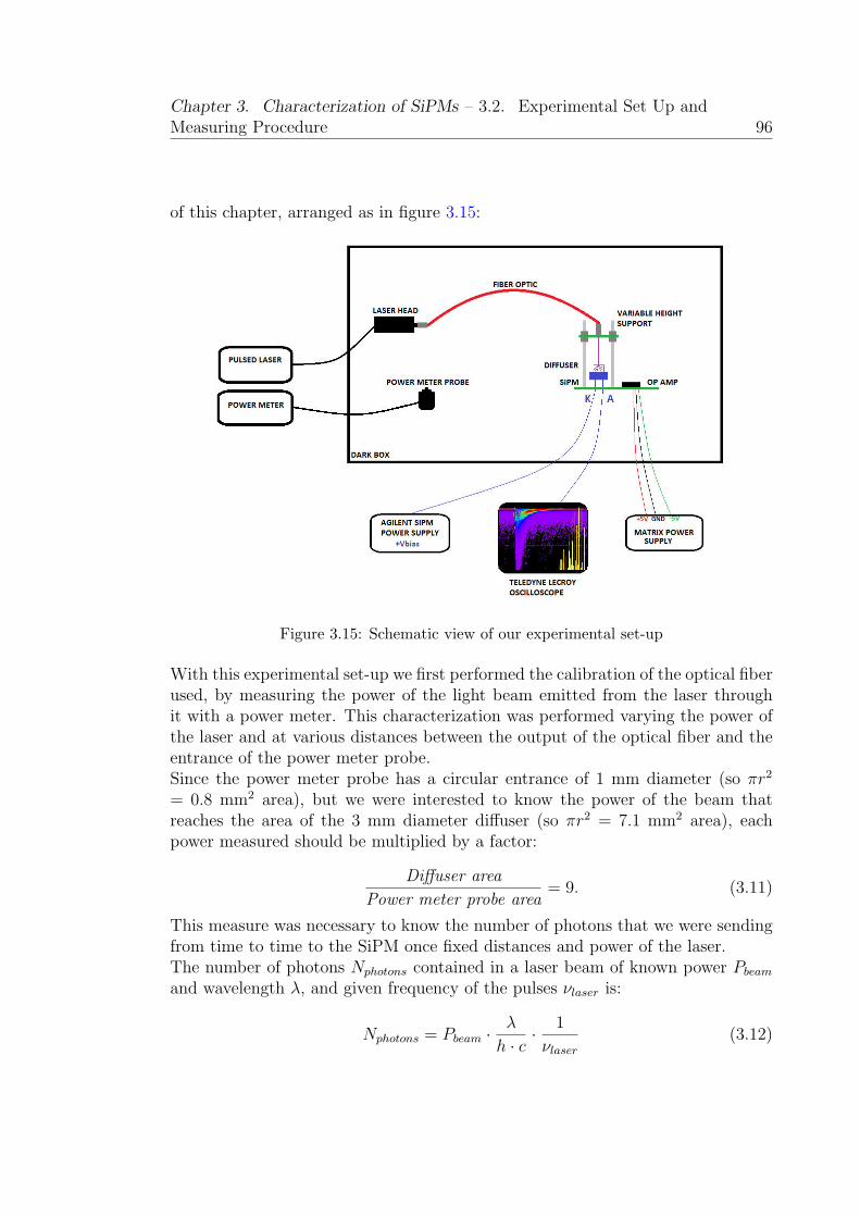
Chapter 3. Characterization of SiPMs – 3.2. Experimental Set Up andMeasuring Procedure 96
of this chapter, arranged as in figure 3.15:
Figure 3.15: Schematic view of our experimental set-up
With this experimental set-up we first performed the calibration of the optical fiberused, by measuring the power of the light beam emitted from the laser throughit with a power meter. This characterization was performed varying the power ofthe laser and at various distances between the output of the optical fiber and theentrance of the power meter probe.Since the power meter probe has a circular entrance of 1 mm diameter (so πr2
= 0.8 mm2 area), but we were interested to know the power of the beam thatreaches the area of the 3 mm diameter diffuser (so πr2 = 7.1 mm2 area), eachpower measured should be multiplied by a factor:
Diffuser area
Power meter probe area= 9. (3.11)
This measure was necessary to know the number of photons that we were sendingfrom time to time to the SiPM once fixed distances and power of the laser.The number of photons Nphotons contained in a laser beam of known power Pbeam
and wavelength λ, and given frequency of the pulses νlaser is:
Nphotons = Pbeam · λ
h · c ·1
νlaser(3.12)

Chapter 3. Characterization of SiPMs – 3.2. Experimental Set Up andMeasuring Procedure 97
Our laser is Gaussian, so its intensity profile in a plane perpendicular to the propa-gation direction (or better its spot) follows a Gaussian distribution (fig. 3.16 left).This fact obviously limits our capability of focusing uniformly photons over thewhole SiPM surface. To solve this problem we put a 3 millimeters diameter opalduffusing glass on the SiPM surface. This device have one surface flashed with amilky white opal coating which allows it to diffuse light evenly so it can be used toachieve a near Lambertian distribution6 (fig. 3.16 right) so we were more or lessguaranteed to illuminate the entire surface of the SiPM uniformly.
Figure 3.16: On the left: transverse intensity profile of a Gaussian beam that is prop-
agating out of the page. Blue curve: electric (or magnetic) field amplitude vs. radial
position from the beam axis. The black curve is the corresponding intensity. On the
right: radiation pattern for diffuse photons passing through the diffusing glass
However, the level of diffusion in the opal glass causes a large amount of scatteringloss. Indeed, using the power meter, we measured the optical power of a lightbeam with and without the opal diffusing glass placed in front of the entrance ofthe probe. From this test we found that the diffuser cuts ∼ 70% of the initialbeam, then only ∼ 30% arrives on the SiPM surface.Moreover, the diffuser area is 7.1 mm2 but the SiPM’s area is 9 mm2 (fig. 3.17),so the diffuser does not cover the entire detection area of the SiPM.
6See appendix A for more details

Chapter 3. Characterization of SiPMs – 3.2. Experimental Set Up andMeasuring Procedure 98
Figure 3.17: Area of the SiPM covered by the diffuser
From the following simple relation:
Ncells : AreaSiPM = x : Areadiffuser, (3.13)
we calculated the actual number of cells stricken by photons = 2840.Taking account of these considerations, we proceeded to the measurement of theSiPM response by targeting it with the light beam outgoing from the opticalsystem described above, setting 100kHz frequency on the light pulser, for a rangeof incident photons that goes from a maximum of 23819 to a minimum of 155 forevery pulse7, suppliyng the SiPM with its operation voltage (VOP = 54.8V) andsetting the trigger on the laser output signal.But, when we turned on the SiPM in high light levels conditions, another problememerged: the output signals from the SiPM for a high number of incident photons(from 1000 incident photons) is greater than 5V. But 5V is the dual power supplyvoltage of the amplifier and of course it is impossible that the amplifier can produceon its output a voltage signal larger than its own supply voltage. Indeed the signaldisplayed on the oscilloscope appeared neatly cut close to 5V (fig. 3.18).To remedy this other problem, we have lowered the gain of the operational amplifierreplacing its feedback resistor (1500 Ω) with a lower value resistor (220 Ω). So,referring to figure 3.5, the new amplification factor is given by:
G =Rf
R2
=220Ω
75Ω= 2.93 (3.14)
In this configuration the first peak amplitude is no more 10mV but 1.5 mV and,for the maximum number of incident photons in this set-up, the signal read fromthe oscilloscope have an amplitude of 4.114 V, so it was far enough away from thesupply voltage of the operational amplifier as not to be cut.At this point we were able to perform the measurement descripted above, so wehave set the oscilloscope trigger on the signal coming from the laser and then we
7Thi aim was achieved by changing the output power of the light pulser
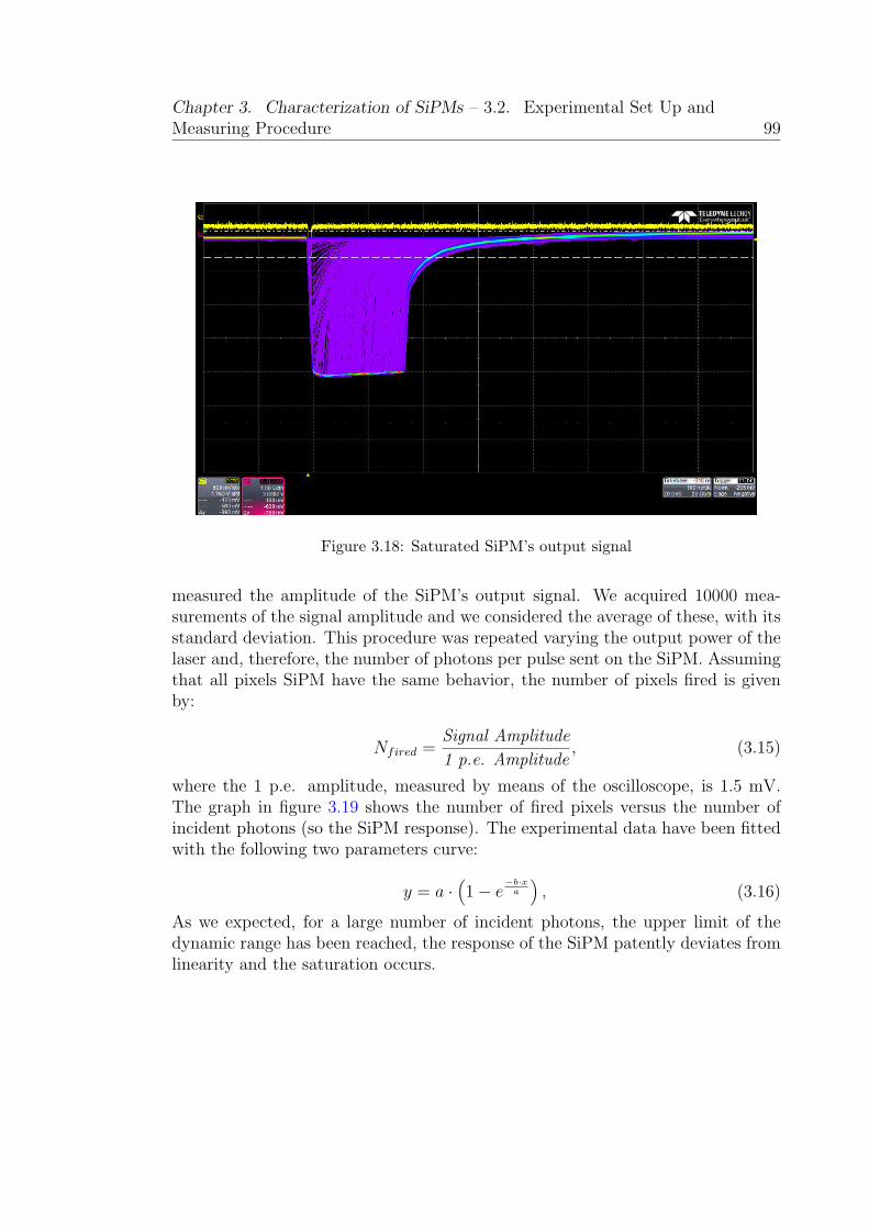
Chapter 3. Characterization of SiPMs – 3.2. Experimental Set Up andMeasuring Procedure 99
Figure 3.18: Saturated SiPM’s output signal
measured the amplitude of the SiPM’s output signal. We acquired 10000 mea-surements of the signal amplitude and we considered the average of these, with itsstandard deviation. This procedure was repeated varying the output power of thelaser and, therefore, the number of photons per pulse sent on the SiPM. Assumingthat all pixels SiPM have the same behavior, the number of pixels fired is givenby:
Nfired =Signal Amplitude
1 p.e. Amplitude, (3.15)
where the 1 p.e. amplitude, measured by means of the oscilloscope, is 1.5 mV.The graph in figure 3.19 shows the number of fired pixels versus the number ofincident photons (so the SiPM response). The experimental data have been fittedwith the following two parameters curve:
y = a ·(
1− e−b·xa
)
, (3.16)
As we expected, for a large number of incident photons, the upper limit of thedynamic range has been reached, the response of the SiPM patently deviates fromlinearity and the saturation occurs.

Chapter 3. Characterization of SiPMs – 3.2. Experimental Set Up andMeasuring Procedure 100
Figure 3.19: Number of fired pixels as a function of the number of incident photons with
a zoom on the linear part of the curve
The two parameters a and b provide the total number of the SiPM cells and itsPDE respectively:
a = Ncells = 2769± 32 (3.17)
b = PDE = (40.9± 0.9)% (3.18)
The value of the parameter a is very near to the total number of illuminated cells(2840 as discussed above) and since the PDE provided by the SiPM’s datasheet is40% the value of the parameter b is in very in good agreement with the nominalvalue.

Chapter 3. Characterization of SiPMs – 3.3. Final Considerations 101
3.3 Final Considerations
The detailed analysis we have done is needed to describe the state of art for silicondetectors in order to choose the core device for the realization of the next VSiPMTprototype.The SiPMs examined in this chapter are designed specifically to a correct operationof the VSiPMT, indeed they are windowless and p-over-n type. In particular wehave seen that the latest generation devices, belonging to the S13360 series, offersuperior performances in terms of dark rate and requires a lower operation voltage.Very recently further improvements have been made in this series, indeed by July2016 the S13360-(x)VE are on the market (fig. 3.20).
Figure 3.20: Very latest Hamamatsu MPPCs’ datasheet
These are devices optimized for precision measurements miniaturized by the use ofTSV (through-silicon via) and CSP (chip size package) technologies. The adoptionof the TSV structure made possible to eliminate wiring on the photosensitive areaside. Since no electrode space for wire bonding is needed, the gap between thepackage edge and the SiPM photosensitive area around the outer periphery isreduced to 0.2 mm on the four sides, allowing a four-side buttable arrangement.This results in a compact structure with little dead spaces compared to previousproducts. Moreover, this four side buttable structure allows multiple devices to bearranged side by side to fabricate large area devices.In particular we are interested in the S13360-6050VE, that is optimized for medicalimaging and high-energy particle detection, measurements which require photoncounting in low light level conditions. Its characteristics are summarized in figure3.21. It has a very large number of cells (14336) but at the same time a high fillfactor (74%). This allows to greatly expand the dynamic range without affectingthe PDE, which remains the same as the device had 3500 cells (40%).The only drawback of this device is the high dark counts rate (2 Mcps at 0.5p.e. treshold), obviously due to the large number of cells. However, in a realistic

Chapter 3. Characterization of SiPMs – 3.3. Final Considerations 102
Figure 3.21: Electrical, optical and structural characteristics of the S13360-6050VE at
25C evidenced in purple
experiment unlikely we would have to disclose a single photon. So we can choosea higher treshold for our trigger (4 or 5 p.e.) and cut away this noise.
Chapter 4
The Temperature Issue
As we have seen in the previous part, astroparticle detection in our area of interestsis based on phenomena related to light emission. To obtain better measurementconditions facilities, experiments and laboratories involved in astroparticle physicshave to be put in places that can ensure the lowest possible light pollution, suchas:
• the top of a mountain (like the telescope MAGIC1 that is situated on theRoque de los Muchachos on La Palma, one of the Canary Islands);
• the middle of a desert (like the High Resolution Fly’s Eye or HiRes detector,in the western Utah desert in the USA);
• the space (like PAMELA2, mounted on the upward-facing side of the Resurs-DK1 Russian satellite);
• under ice (like IceCube, a neutrino telescope constructed at the Amundsen-Scott South Pole Station in Antarctica, its thousands of sensors are dis-tributed over a cubic kilometre of volume under the Antarctic ice);
• under the sea (like KM3NeT3, a neutrino telescope located in the deepestseas of the Mediterranean).
These locations (especially the desert, the space and the mountain) are character-ized by large temperature variations and, since the detectors of our interest arebased on semiconductor devices technology, efforts must be devoted to temperaturecompensation issues.
1Acronym for: Major Atmospheric Gamma-ray Imaging Cherenkov Telescope2Acronym for: Payload for Antimatter Matter Exploration and Light-nuclei Astrophysics3Acronym for: Cubic Kilometre Neutrino Telescope
103

Chapter 4. The Temperature Issue – 104
4.0.1 SiPM Characterization in Temperature With a Stan-dard Power Supply
As we have seen in the first part of this thsis, semiconductor devices are extremelysensitive to temperature changes. In particular in a constant temperature environ-ment, the overvoltage VOV applied to a SiPM determines its operational charac-teristics such as gain and PDE. But, since temperature affects the opto-electricalcharacteristics of a p-n junction such as the width of the depletion region, thebreakdown voltage, band-gap energy, resistivity, and more, the operation of aSiPM will be strongly affected by this parameter. An example of this dependenceis the recovery time of a pixel from avalanche. The characteristic recovery time isthe RC time constant determined by the values of the junction capacitance Cd andof the quenching resistor Rq. For a given VOV , temperature affects the width ofthe depletion region and, thus, Cd. It also affects the resistance of the polysiliconquenching resistor Rq. Thus, the product of these two quantities can also changewith temperature affecting the recovery time.To verify the overvoltage’s temperature dependence, we have performed a study onthe SiPM family S10931-100P that consisted in a current-voltage characterizationunder temperature variations. The experimental set-up consists of the followinginstrumentation:
• Angelantoni’s environmental test chamber;
• Keithley picoammeter;
• Agilent power supply;
• The SiPM S10931-100P;
• A program written in LabVIEW that interfaces with the picoammeter andwith the power supply.
In order to perform this test we connected the SiPM’s anode to the power supplyand the cathode to the picoammeter (fig. 4.1). Since we wanted to show that thebreakdown voltage of the SiPM depends on the temperature, we were interestedin studying the behavior of the SiPM in the region of its characteristic V-I curvecorresponding to the reverse bias region. So we sent a negative voltage to theanode with respect to the cathode, in order to have a reverse biased SiPM.Since our SiPM datasheet do not provide the device’s breakdown voltage but justa recommended operating voltage VOP , we will refer to the latter characteristicquantity for the following analysis.We set the environmental chamber so that its internal temperature varied from

Chapter 4. The Temperature Issue – 105
Figure 4.1: Schematic configuration of the experimental set-up for the V-I curve versus
temperature test.
45C to 5C in steps of 5C, and for every step we performed a V-I curve character-ization in a voltage range that goes from 50V to 73.8V (so with a 2V overvoltagesince the SiPM we have characterized had VOP=71.8V ).Then we put all these curves on the same graph and the result of this characteri-zation is shown in figure 4.2.For all these measures the environmental humidity has been set to 20%.Then, we considered the current level corresponding to the VOP of the charac-teristic curve at 25C (it was 2.686279 µA) and we saw which were the values ofthe voltage corresponding to this current on the other curves tracing the orizontalintercept on the graph. We put these values in a graph where X-axis shows tem-peratures set from time to time in the environmental chamber and Y-axis showsvoltage levels corresponding to 2.686279 µA current for each curve. The result ofthis operation is shown below (fig. 4.3)The graph clearly shows what we already expected, i.e. the fact that the VOP ,or equivalently the SiPM’s breakdown voltage, increases with temperature and,in the temperature range explored for this analysis, this increase is linear with aslope ∆V
∆T= (55.5077 ± 0.5274) mV/C, in good agreement with the nominal value
provided by the datasheet (∆V∆T
= 56 mV/C). The consequences of this behaviorwill affect the gain of the device. Indeed, as we saw in the previous part, the gainof a SiPM is given by the following formula:
G(VOV ) =Cd · VOV
e(4.1)
Gain is directly proportional to VOV . We just saw that, at a given fixed bias, thebreakdown voltage increases with temperature so, since by definition VOV is givenby:

Chapter 4. The Temperature Issue – 106
Figure 4.2: V-I curves of the SiPM S10931-100P-3023 performed under temperature
variations
VOV = Vbias − VBD, (4.2)
we expect that the gain decreases with increasing temperature. To verifythis fact we have performed a study on the SiPM family S10931-100P that consistedin a gain characterization under temperature variations.The experimental set-up consists of the following instrumentation arranged as infigure 4.4:
• Angelantoni’s environmental test chamber;
• Electronic board made ad hoc for the SiPM’s signal amplification on whichthe SiPM and a current voltage amplifier are mounted;
• DC voltage generator Agilent 0.1V sensitivity mod. E3612A used as a powersupply for the SiPM;
• DC voltage generator Matrix mod. MPS-3005-L-3 used as a dual powersupply for the signal amplifier mounted on the electronic board;
• Digital Teledine LeCroy serial data analyzer mod. SDA 760Zi-A, 4 inputchannels, 6 GHz bandwidth with 40 GS/s sample rate.

Chapter 4. The Temperature Issue – 107
Figure 4.3: VOP versus temperature variations
• The SiPM S10931-100P;
Figure 4.4: Schematic view of our experimental set-up
Fixed the Vbias at the device’s VOP (71.8V) this measurement was performed by

Chapter 4. The Temperature Issue – 108
varying the value of the environmental tempeature between 5C and 45C by 5Csteps by means of the environmental chamber. The data acquisition and analysiswas performed following the same procedure described in section 3.2.1, with thedifference that this time the SiPM was in dark so we set the trigger on the signalitself at 0.5 p.e. The results of this analisys are shown in the graph below (fig.4.5).
Figure 4.5: Gain of the SiPM S10931-100P as a function of temperature using a standard
power supply
As expected, for a given bias voltage, the gain decreases linearly with increasingtemperature.Physically this phenomenon is explained by the fact that as the temperature in-creases, the Boltzmann distribution implies an increasing fraction of electrons inthe conduction band and, thus, a decreasing resistivity of the semiconductor. Be-cause the quenching resistor is made from polysilicon, Rq will decrease with in-creasing temperature. The junction capacitance, Cd, also varies with temperature.With zero bias, Cd ∝ 1√
VBI, where VBI is the p-n junction built-in voltage. Be-
cause VBI decreases with temperature, Cd increases with temperature.To solve the problem linked to temperature variations, which represents a seriouslimitation to the SiPM’s performaces, and then to the VSiPMT’s performances,we experienced a new electronic device manufactured by Hamamatsu which com-pensates the overvoltage at different temperatures.
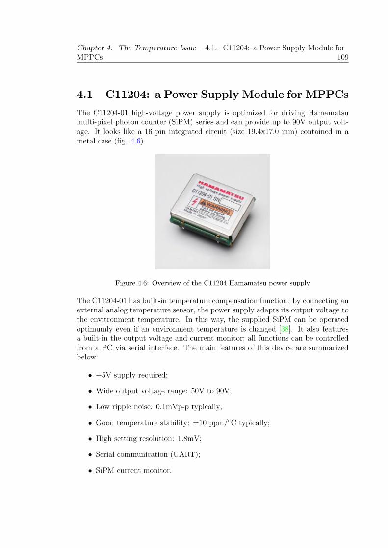
Chapter 4. The Temperature Issue – 4.1. C11204: a Power Supply Module forMPPCs 109
4.1 C11204: a Power Supply Module for MPPCs
The C11204-01 high-voltage power supply is optimized for driving Hamamatsumulti-pixel photon counter (SiPM) series and can provide up to 90V output volt-age. It looks like a 16 pin integrated circuit (size 19.4x17.0 mm) contained in ametal case (fig. 4.6)
Figure 4.6: Overview of the C11204 Hamamatsu power supply
The C11204-01 has built-in temperature compensation function: by connecting anexternal analog temperature sensor, the power supply adapts its output voltage tothe envitronment temperature. In this way, the supplied SiPM can be operatedoptimumly even if an environment temperature is changed [38]. It also featuresa built-in the output voltage and current monitor; all functions can be controlledfrom a PC via serial interface. The main features of this device are summarizedbelow:
• +5V supply required;
• Wide output voltage range: 50V to 90V;
• Low ripple noise: 0.1mVp-p typically;
• Good temperature stability: ±10 ppm/C typically;
• High setting resolution: 1.8mV;
• Serial communication (UART);
• SiPM current monitor.

Chapter 4. The Temperature Issue – 4.1. C11204: a Power Supply Module forMPPCs 110
• Current absorption: 22 mA;
It also has many funtions such as the ”Monitor”, which provide output voltage+HV[V], output current Id[mA], and external temperature sensor value T[C], the”ON/OFF switch” and the ”Overcurrent protection”, which stops the output ofthe high voltage when the current exceedes a 3mA threshold for more then fourseconds.But the most interesting feature is certainly the ”Setup”. This function can setthe output voltage to any value by setting the reference voltage Vb[V], the ref-erence temperature Tb[
C], the primary temperature coefficient ∆V∆T
[mV/C], andthe secondly temperature coefficient ∆V
∆T 2 [mV/C2]. In particular, by means of thelatter two correction factors, a temperature compensation of the output voltagecan be performed. More precisely, using the temperature T[C] of the externaltemperature sensor, the output voltage +HV[V] is determined by the followingformula:
+HV =∆V∆T 2 · (T − Tb)
2 + ∆V∆T
· (T − Tb)
1000+ Vb (4.3)
Moreover, temperature coefficients can be set to four parameters: two for thehigh temperature (HT) side (∆V
∆T)1[mV/C] and ( ∆V
∆T 2 )1[mV/C2] (for temperatureshigher than the reference temperature Tb) and two for the low temperature (LT)side (∆V
∆T)2[mV/C] and ( ∆V
∆T 2 )2[mV/C2] (for temperatures lower than the referencetemperature Tb). So it is possible to set different correction factors for the outputvoltage above and below the reference temperature (fig. 4.7).
Figure 4.7: Output voltage versus temperature with different correction factors
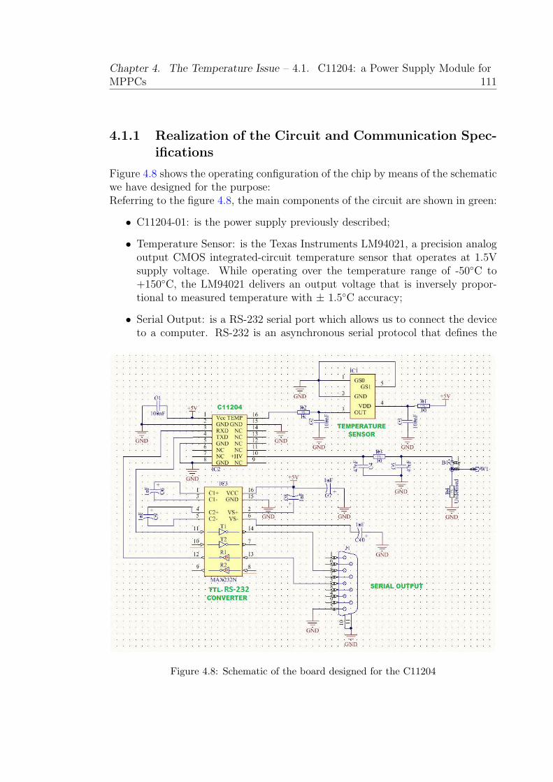
Chapter 4. The Temperature Issue – 4.1. C11204: a Power Supply Module forMPPCs 111
4.1.1 Realization of the Circuit and Communication Spec-ifications
Figure 4.8 shows the operating configuration of the chip by means of the schematicwe have designed for the purpose:Referring to the figure 4.8, the main components of the circuit are shown in green:
• C11204-01: is the power supply previously described;
• Temperature Sensor: is the Texas Instruments LM94021, a precision analogoutput CMOS integrated-circuit temperature sensor that operates at 1.5Vsupply voltage. While operating over the temperature range of -50C to+150C, the LM94021 delivers an output voltage that is inversely propor-tional to measured temperature with ± 1.5C accuracy;
• Serial Output: is a RS-232 serial port which allows us to connect the deviceto a computer. RS-232 is an asynchronous serial protocol that defines the
Figure 4.8: Schematic of the board designed for the C11204
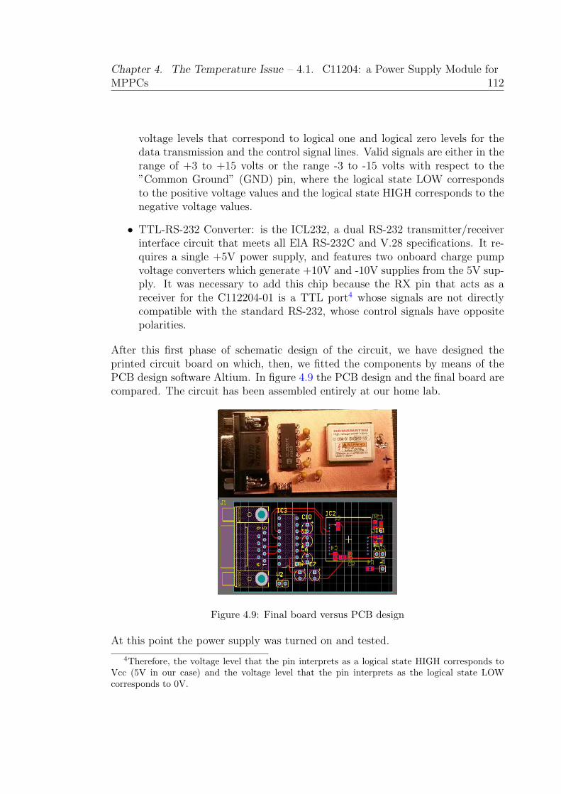
Chapter 4. The Temperature Issue – 4.1. C11204: a Power Supply Module forMPPCs 112
voltage levels that correspond to logical one and logical zero levels for thedata transmission and the control signal lines. Valid signals are either in therange of +3 to +15 volts or the range -3 to -15 volts with respect to the”Common Ground” (GND) pin, where the logical state LOW correspondsto the positive voltage values and the logical state HIGH corresponds to thenegative voltage values.
• TTL-RS-232 Converter: is the ICL232, a dual RS-232 transmitter/receiverinterface circuit that meets all ElA RS-232C and V.28 specifications. It re-quires a single +5V power supply, and features two onboard charge pumpvoltage converters which generate +10V and -10V supplies from the 5V sup-ply. It was necessary to add this chip because the RX pin that acts as areceiver for the C112204-01 is a TTL port4 whose signals are not directlycompatible with the standard RS-232, whose control signals have oppositepolarities.
After this first phase of schematic design of the circuit, we have designed theprinted circuit board on which, then, we fitted the components by means of thePCB design software Altium. In figure 4.9 the PCB design and the final board arecompared. The circuit has been assembled entirely at our home lab.
Figure 4.9: Final board versus PCB design
At this point the power supply was turned on and tested.
4Therefore, the voltage level that the pin interprets as a logical state HIGH corresponds toVcc (5V in our case) and the voltage level that the pin interprets as the logical state LOWcorresponds to 0V.

Chapter 4. The Temperature Issue – 4.1. C11204: a Power Supply Module forMPPCs 113
C11204-01 is communicated in UART communication protocol so, roughly speak-ing, it is provided with a universal asynchronous receiver/transmitter that takesbytes of data and transmits the individual bits in a sequential fashion by means ofthe pins RX and TX. At the destination, a second UART re-assembles the bits intocomplete bytes. Each UART contains a shift register, which is the fundamentalmethod of conversion between serial and parallel forms. Regarding the receiver, alloperations of the UART hardware are controlled by a clock signal which runs at amultiple of the data rate, typically 8 times the bit rate. The receiver tests the stateof the incoming signal on each clock pulse, looking for the beginning of the startbit. If the apparent start bit lasts at least one-half of the bit time, it is valid andsignals the start of a new character. If not, it is considered a spurious pulse and isignored. After waiting a further bit time, the state of the line is again sampled andthe resulting level clocked into a shift register. After the required number of bitperiods for the character length (8 bits in this case) have elapsed, the contents ofthe shift register are made available (in parallel fashion) to the receiving system.The UART will set a flag indicating new data is available, and may also generate aprocessor interrupt to request that the host processor transfers the received data.Regarding the transmitter, operations are simpler as the timing does not have tobe determined from the line state, nor is it bound to any fixed timing intervals.Transmitting and receiving UARTs must be set for the same bit speed (or baudrate), character length, parity, and stop bits for proper operation; in particularUART communication specifications for C11204-01 are as follows:
• Baud Rate: 38400 bits per second;
• Data Bit: 8;
• Parity Bit: even;
• Stop Bit: 1;
• Flow Control: none;
• Data Order : LSB;
When C11204-01 receives the command from the host (our personal computerin this case), performs a process according to the command type (there alwaysis a response to the command) and, by analyzing the contents of the commandresponse, the exchange of data between the host and the power supply is performed.The command character code is ASCII5, an example of sent and received commandformat is shown below (fig. 4.10), for more details about C11204-01 communicationprotocol refer to the device Command Reference [39].
5Acronym for American Standard Code for Information Interchange, is a character encodingstandard

Chapter 4. The Temperature Issue – 4.1. C11204: a Power Supply Module forMPPCs 114
Figure 4.10: Example of sent and received commands, the characters that are not de-
scribed in the figure are the header and delimiter of the string of characters (STX and
CR), the end of the stecific command (ETX) and the error check (EC)
The commands were sent and received by means of the open source terminalTermite but, since each response that came from the power supply had to betranslated from ASCII to Exadecimal and then from Exadecimal to dimensioneddecimal numbers to have temperatures, voltages and currents, this way to controlthe device was found to be definitely cumbersome.So we realized, thanks to the help of Dr. Riccardo de Asmundis, senior researcherat the INFN, a LabView interface (fig. 4.11) that would facilitate the communi-cation. By means of this interface it is possible to easily set the four temperaturecompensation factors for HT and LT sides, the reference voltage, the referencetemperature and the initial voltage level by directly entering their values in voltsand degrees centigrade. The interface also provides a real time readout of theoutput voltage level, the current level and the temperature measured by the tem-perature sensor so we can check at any time the state of the system.For this specific purpose the device drivers of C11204-01 were designed by Dr.Riccardo de Asmundis.

Chapter 4. The Temperature Issue – 4.1. C11204: a Power Supply Module forMPPCs 115
Figure 4.11: Screen of the LabVIEW control interface for C11204-01
4.1.2 C11204-01 Calibration and Test
To test the device we used the following experimental set-up, arranged as shownin figure 4.12:
• Angelantoni’s environmental test chamber;
• Agilent power supply;
• The C11204-01 board;
• The LabVIEW control interface for C11204-01
We first verified that the temperature sensor was correctly calibrated. Then we setthe environmental chamber so that its internal temperature varied from 45C to15C in steps of 2C, and for every step we read the temperature measured by the

Chapter 4. The Temperature Issue – 4.1. C11204: a Power Supply Module forMPPCs 116
Figure 4.12: Experimental set-up for calibration and test of C11204-01
sensor. For all these measures the environmental humidity has been set to 17%.The results of this calibration are shown in the graph in figure 4.13, where X-axis shows temperatures set from time to time in the environmental chamber andY-axis shows temperatures read by the sensor.
Figure 4.13: Trend curve of the temperature sensor calibration. χ2 = 0.018, slope =
1.0006 ± 0.0009

Chapter 4. The Temperature Issue – 4.1. C11204: a Power Supply Module forMPPCs 117
The linear trend of the temperatures read by the sensor with respect to those setin the environmental chamber shows that the sensor is well calibrated.Finally, to verify that the power supply worked properly we set to 0 mV/C2 thevalue of the secondary temperature coefficient and to 1000 mV/C the value ofthe primary temperature coefficient with 60V reference voltage and 25C referencetemperature. With this choice for the coefficients, the C11204-01 should modifythe output power supply voltage of 1V for each 1C temperature variation. Soagain we set the environmental chamber so that its internal temperature variedfrom 45C to 15C in steps of 2C, and for every step we read the output voltage.For all these measures the environmental humidity has been set to 17%.The results of this test are shown in the graph in figure 4.14, where X-axis showstemperatures set from time to time in the environmental chamber and Y-axisshows the output voltage.
Figure 4.14: Trend curve of the power supply response. χ2 = 0.31, slope = 0.977 ±0.004
The linear trend of the output voltage with respect to temperature variations inthe environmental chamber shows that the power supply is working as expected.

Chapter 4. The Temperature Issue – 4.1. C11204: a Power Supply Module forMPPCs 118
4.1.3 SiPM Characterization in Temperature With C11204-01
Found that the circuit was working properly, we performed a gain characterizationin temperature for the SiPM S10931-100P using the C11204-01 as power supply(fig. 4.15).
Figure 4.15: Schematic view of our experimental set-up
As seen in section 4.0.1, the breakdown voltage of the SiPM S10931-100P linearlyincreases of (55.5077 ± 0.5274) mV for every 1C temperature increase. So we setthe C11204-01 reference temperature to 25, the reference voltage to 71.8V (that isthe nominal VOP at 25C), the primary temperature coefficient ∆V
∆Tto 56 mV/C,
and the secondly temperature coefficient ∆V∆T 2 to 0 mV/C2 to turn on the device’s
built-in temperature compensation function.Then we performed measurements in the same way described in section 4.0.1 andthe results are shown in the graph below (fig. 4.16).From this graph it is evident that the gain in this case is always between M = 2 andM = 2.4, where the nominal gain of this device is M = 2.4. From the comparison

Chapter 4. The Temperature Issue – 4.1. C11204: a Power Supply Module forMPPCs 119
Figure 4.16: Gain of the SiPM S10931-100P as function of temperature using C11204-01
power supply
between the gain measurements as function of temperature variations, performedwith a standard power supply and with the C11204-01, it is easy to see the clearimprovement in SiPM’s performances.Indeed, with a standard power supply, as temperature increases, the gain decreasesuntil the device turns off at 45C; this is manifested by the gradual decrease in theamplitude of the SiPM’s output signal, as we see in figure 4.17).
Figure 4.17: S10931-100P SiPM’s output signals supplied with a standard power supply
for (from left to right) 35C, 40C and 45C environment temperatures. Notice that
SiPM’s signals have their amplitude significantly reduced as the environment tempera-
ture increases
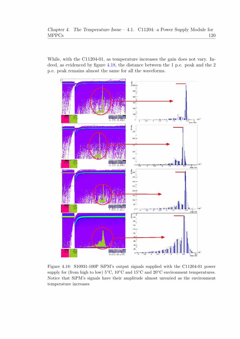
Chapter 4. The Temperature Issue – 4.1. C11204: a Power Supply Module forMPPCs 120
While, with the C11204-01, as temperature increases the gain does not vary. In-deed, as evidenced by figure 4.18, the distance between the 1 p.e. peak and the 2p.e. peak remains almost the same for all the waveforms.
Figure 4.18: S10931-100P SiPM’s output signals supplied with the C11204-01 power
supply for (from high to low) 5C, 10C and 15C and 20C environment temperatures.
Notice that SiPM’s signals have their amplitude almost unvaried as the environment
temperature increases

Chapter 4. The Temperature Issue – 4.1. C11204: a Power Supply Module forMPPCs 121
The only drawback of this device is that it can’t clear the signal from thermal noise(the shrewd reader has certainly noticed the huge noise band that affects signalson the lower side of the figure 4.18). But it must be said that this analysis wasperformed on a very old generation SiPM with large pixels and high dark countsrate. The situation improves significantly if we use the latest generation SiPM.
Figure 4.19: Comparison between S13360-4929 SiPM’s output signals supplied with a
standard power supply (left) and with the C11204-01 (right) for (from high to low) 35C,
40C and 45C environment temperatures
Notice that the new generation SiPM’s signals on the right have their amplitude notvery significantly reduced as the environment temperature increases. This appensbecause of the small temperature coefficient and the better overall features of thisdevice with respect to the old generation due to the improvement of materialand wafer process thecnology. An interesting study could be performed in thisdirection.

Chapter 5
The Latest Usable VSiPMTPrototype
The VSiPMT project went on with a theoretical study of feasibility combined withGeant4-based simulations to find the range of the electrons in the SiPM. The firstproof of feasibility [41] arrived in 2012, when the response of a special SiPM, aselectron multiplier, was tested with an electron beam extracted at the TTT3 ac-celerator available in the Physics Department of the University of Naples.The results obtained convinced Hamamtsu Photonics, a world leader company inphotodetector manufacturing, to realize for professor Barbarino’s research grouptwo VSiPMT prototypes to start to explore the potentialities of the device: EB-MPPC050 (ZJ5025) and EB-MPPC100 (ZJ4991).The characterization of these first two prototypes of VSiPMT put up really encour-aging results [42]. The devices exhibit outstanding properties and performancesbeyond expectations, neverthless, they were no usable because of the small size (3mm diameter photocathode) and the reduced dynamic range; these problems aredue to the fact that these two prototypes were just testing devices, manufacturedto verify the properties found during the feasibility tests. Anyway Hamamatsu im-proved these two features and assembled the device: prototype EB-MPPC100(XE2597) 1 INCH, the first really usable VSiPMT prototype. A picture of it isshown in figure 5.1.The absence of the dynode chain entails a visible consequence: the device is small.
122

Chapter 5. The Latest Usable VSiPMT Prototype – 123
Figure 5.1: Picture of the VSiPMT prototype (side view) together with the dimensional
outline of the device in mm
This prototype was made from a standard PMT, whereby all connections avail-able (which originally served as connections for the dynodes) only two are usedeffectively: the one for the SiPM supply and the one for the readout signal (fig.5.2).
Figure 5.2: Detail of the connenctions
Under a Borosilicate Glass round window ( Φ = 25 mm diameter) is deposited acircular Bialkali photocathode (22 mm diameter), where photo-electron conversion

Chapter 5. The Latest Usable VSiPMT Prototype – 124
occurs. The Bialkali photocathode offers a good quantum efficiency optimizedfor the detection of Near Ultraviolet radiations (NUV 300÷400 nm wavelength).Indeed the photocathode spectral response (shown in figure 5.3) have the QE peakvalue (about 15%) for an incident wavelength λ = 350 nm. In our case (407 nmwavelenght) QE ∼ 12%.
Figure 5.3: Photocathode spectral response
A single stage focusing system is present to drive the photoelectrons on the SiEM.It is composed by a focusing ring kept at the same potential with respect to theHV applied to the photocathode. The system is accomodated into a cylindricalglass case of 44 mm length.In this prototype a special windowless SiPM is mounted, the absence of the pro-tective entrance window eases the entrance of the photoelectrons into the Silicon.Moreover, the SiPM used is realized in a p+nn+ configuration for EDE optimiza-tion, as explained in the first part of this thesis (SiEM).Characteristics and recommended work conditions are summrized below:
• SiEM area: 3 x 3 mm2;
• number of pixels: 900 of size 100 x 100 µm2;
• fill factor: 78%;
• optimized configuration: p+nn+;
• SiEM operation voltage: +71.5 V;
• photocathode power supply: −1.9 kV.
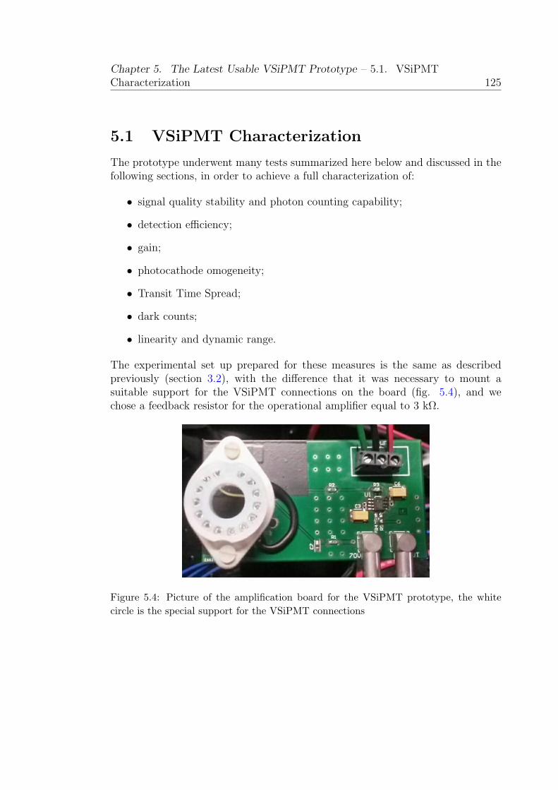
Chapter 5. The Latest Usable VSiPMT Prototype – 5.1. VSiPMTCharacterization 125
5.1 VSiPMT Characterization
The prototype underwent many tests summarized here below and discussed in thefollowing sections, in order to achieve a full characterization of:
• signal quality stability and photon counting capability;
• detection efficiency;
• gain;
• photocathode omogeneity;
• Transit Time Spread;
• dark counts;
• linearity and dynamic range.
The experimental set up prepared for these measures is the same as describedpreviously (section 3.2), with the difference that it was necessary to mount asuitable support for the VSiPMT connections on the board (fig. 5.4), and wechose a feedback resistor for the operational amplifier equal to 3 kΩ.
Figure 5.4: Picture of the amplification board for the VSiPMT prototype, the white
circle is the special support for the VSiPMT connections
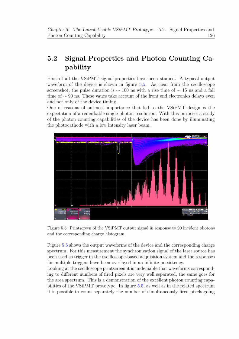
Chapter 5. The Latest Usable VSiPMT Prototype – 5.2. Signal Properties andPhoton Counting Capability 126
5.2 Signal Properties and Photon Counting Ca-
pability
First of all the VSiPMT signal properties have been studied. A typical outputwaveform of the device is shown in figure 5.5. As clear from the oscilloscopescreenshot, the pulse duration is ∼ 100 ns with a rise time of ∼ 15 ns and a falltime of ∼ 90 ns. These vaues take account of the front end electronics delays evenand not only of the device timing.One of reasons of outmost importance that led to the VSiPMT design is theexpectation of a remarkable single photon resolution. With this purpose, a studyof the photon counting capabilities of the device has been done by illuminatingthe photocathode with a low intensity laser beam.
Figure 5.5: Printscreen of the VSiPMT output signal in response to 90 incident photons
and the corresponding charge histogram
Figure 5.5 shows the output waveforms of the device and the corresponding chargespectrum. For this measurement the synchronization signal of the laser source hasbeen used as trigger in the oscilloscope-based acquisition system and the responsesfor multiple triggers have been overlayed in an infinite persistency.Looking at the oscilloscope printscreen it is undeniable that waveforms correspond-ing to different numbers of fired pixels are very well separated, the same goes forthe area spectrum. This is a demonstration of the excellent photon counting capa-bilities of the VSiPMT prototype. In figure 5.5, as well as in the related spectrumit is possible to count separately the number of simultaneously fired pixels going

Chapter 5. The Latest Usable VSiPMT Prototype – 5.3. Gain 127
from a single pixel up to twelve, a performance simply unreachable by standardPMTs (where photon counting is impossible as evident in figure 5.6) and even bythe recently developed HPDs (where the single peak resolution is not so good be-cause of fluctuations in photon counting, due to the fact that HPDs use junctionswhich work in proportional regime as electron detectors) .
Figure 5.6: Printscreen of the output signal of the Photo multiplier tube TS-80000 series
5.3 Gain
In a VSiPMT the gain is obtained by the electrons crossing the Geiger region ofthe SiEM. Thus, a standard current signal is given for each fired cell. Therefore,for the prototype under test the gain coincides with the gain of the SiEM used.According to the above description, the gain of the SiEM can be defined as thefraction between the charge of the pulse generated from each pixel during thebreakdown process and the charge of the electron. The charge of a single firedpixel can be calculated as the difference between all the possible couples of adjacentpeaks in the charge spectrum shown in figure 5.7.A measure of the SiEM gain as a function of the applied bias voltage in the range[70.8, 71.5] V has been performed, keeping HV = -1.9 kV. The resulting curve (seefig. 5.8) exhibits a very linear trend, with values ranging between [1.3 x 10⁶; 2.6x 10⁶], in fairly good agreement with expectations. The same measure has beenperformed keeping HV off, since the results where the same as if the HV was onthey are not reported here.

Chapter 5. The Latest Usable VSiPMT Prototype – 5.3. Gain 128
Figure 5.7: VSiPMT’s output signal and its spectrum of charge (printscreen fro Teledyne
Lecroy SDA 760Zi 6 GHz Serial data Analyzer). Notice that waveforms corresponding
to different numbers of fired pixels (and so the peaks in the spectrum) are extremely
well separated
Figure 5.8: Graph of gain versus Vbias for the VSiPMT
Chapter 5. The Latest Usable VSiPMT Prototype – 5.4. Noise 129
5.4 Noise
Three are the sources of noise in a VSiPMT: afterpulses, crosstalk and dark rate,widely explained in section 3.2.2.In the first case, the combination of the vacuum tube and the SiEM gives rise toa double contribution: vacuum related afterpulses and SiEM afterpulses.The former are produced by the ionization of residual gases left in the tube afterevacuation or degased materials present in the vacuum silicon photomultiplier tubeafter the evacuation. In this case the arrival time of the afterpulse depends on theion mass and on the HV applied between the photocathode and the SiEM, whilethe afterpulse amplitude depends only on the HV. The second class of afterpulsesis intrinsically related to the SiEM technology [43]. In this case, secondary pulsesare generated by charges carriers that are temporarily trapped by some impuritiesinside the crystal lattice and then released again after some delay which can lastfrom few nanoseconds up to several microseconds.The main noise source in a VSiPMT is represented by dark pulses and crosstalk.Two contributions can be taken into account: thermal electrons emitted at thephotocathode and intrinsic SiEM noise. The latters represent the main contribu-tion, since they have a typical rate ranging between few tens and some hundreds ofkcps per mm2 of active surface, depending on the applied bias voltage. In additionto the strong dependence on the bias voltage, SiPMs dark rate relies heavily onthe pe threshold. For this reason, measurements of the dark count rate at differentbias voltage and different thresholds have been done.The photocathode voltage has been set to -1.9 kV and the bias voltage to differ-ent values: from 71.0 V to 71.6 V in 0.1 V steps. For each of those values hasbeen measured the number of events with peak amplitude above 0.5, 1.5 and 2.5photoelectrons threshold. The results are shown in figure 5.9 and are in excel-lent agreement with the expected dark count rate of the SiEM alone. In order toconfirm the assumption that the main source of dark noise is the SiEM itself, themeasure has been repeated in the same experimental conditions but with no highvoltage applied to the photocathode. The results were absolutely unvaried; in thetable below are collected the values of the dark rates with their errors for the threetresholds at Vbias = VOP = 71.5 V and keeping HV on.

Chapter 5. The Latest Usable VSiPMT Prototype – 5.5. Detection Efficiency:Operating Point 130
Figure 5.9: Dark noise rate as a function of the SiEM overvoltage for the VSiPMT
0.5pe treshold (316, 907 ± 0.564) kcps1.5pe treshold (200.048 ± 0.215) kcps2.5pe treshold (120.211 ± 0.176) kcps
This dark rate seem to be high, the reason lies in the choice of SiEM mountedin the VSiPMT. In the previous chapters several generations of SiPMs have beenconfronted, and we saw that the latest devices differ from the older ones for theirsuperior performances in terms of dark rate. The core device of this VSiPMTprototype clearly belongs to an old generation series (section 3.1.3).However, in a realistic experiment unlikely we would have to disclose a single pho-ton. So we can choose a higher treshold for our trigger (4 or 5 p.e.) and cut awaythis noise, so we foresee an optimistic future in this direction.
5.5 Detection Efficiency: Operating Point
The Photon Detection Effciency (PDE or ǫtot) of the VSiPMT can be defined asthe product of three factors:
ǫtot = ǫPC · ǫgeom · ǫtrigger (5.1)
Where ǫPC is the photocathode’s quantum efficiency, ǫgeom is the geometrical ef-ficiency which takes account of the focusing and the SiEM fill factor and ǫtrigger

Chapter 5. The Latest Usable VSiPMT Prototype – 5.5. Detection Efficiency:Operating Point 131
is the trigger efficiency which takes account of the probability an electron have totrigger an avalanche1. The phenomenology correlated to this latter parameter iswell explained by means of figure 5.10.
Figure 5.10: Schematic view of photoelectrons coming from the photocathode and im-
pinging on the p-over-n SiEM inside the VSiPMT
Referring to the figure, photon n 1 have no energy enough to enter in the p+
region, indeed it stops into the SiO2 insulating layer; photon n 2 have enoughenergy to overcome the SiO2 layer and enter in the p+ region, but its drift is tooshort, the number of pairs produced is to few and the probability that one of themreach the depletion region is low because of the recombination; photon n 3 hasenergy enough to enter in the depletion region and trigger the Geiger avalanche.The range of photoelectrons (that depends on the photoelectron energy after theHV acceleration) inside the SiEM must to be enough to overcome the passivationlayer of SiO2 and a part of p region in such a way that a sufficient number ofelectron-hole pairs are produced.At present we do not know the thickness of the passivation layer SiO2 in frontof the SiEM inside the prototype EB-MPPC100 (XE2597) 1 INCH, but we knowthat the SiEM’s fill factor is ǫgeom = 78% and the photocathode efficiency is ǫPC
= 12%, so by measuring ǫtot (PDE) we can obtain ǫtrigger.The PDE with respect to the high voltage supplied to the photocathode has beenmeasured as follow.The device has been illuminated with few photons per pulse (∼ 70) by using anoptical fibre, during the test the laser beam intensity has been monitored by thepower meter. The PDE is experimentally defined as:
PDE =Npe
Nph
(5.2)
1In first approximation we can say that ǫgeom · ǫtrigger is equal to the EDE defined in section2.4

Chapter 5. The Latest Usable VSiPMT Prototype – 5.5. Detection Efficiency:Operating Point 132
where Npe is the number of fired cells and Nph is the number of photons per laserpulse hitting the photocathode. Once we set the light conditions, we tested thePDE as a function of HV, by varying the photocathode power supply in steps of100 volts. The results of this test are showed in figure 5.11, where is evident thatthe maximum efficiency available is PDE = 2.4%.
Figure 5.11: Results of the photon detection efficiency test in function of the HV
From this measure we expected that, for a certain HV level, the PDE of the devicehad to reach a plateau (a similar analysis has been performed on an old version ofthe VSiPMT prototype, a detailed description of this measurement can be foundin Appendix B)In such a device, the plateau region is linked to the energy threshold of the pho-toelectrons. Therefore, the high voltage is required only to drive photoelectronsto the SiEM surface and to give them the right energy. This is one of the biggestdifferences and advantages of the VSiPMT with respect to other photodetectorcategories. This behaviour comes from the different gain concept applied in theVSiPMT where, as already exstensively illustrated, the high gain is provided bythe geiger avalanche occurring in the SiEM and therefore the PDE doesn’t dependon the photoelectrons energy once they are over the threshold. This means thatonce the device is operated in the plateu region further stabilizations due to highvoltage fluctuations are not necessary.On the contrary, both for PMTs and HPDs the gain strongly depends on thephotoelectron energy. For those devices the higher is the voltage supplied to the
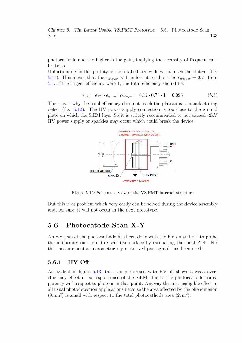
Chapter 5. The Latest Usable VSiPMT Prototype – 5.6. Photocatode ScanX-Y 133
photocathode and the higher is the gain, implying the necessity of frequent cali-brations.Unfortunately in this prototype the total efficiency does not reach the plateau (fig.5.11). This means that the ǫtrigger < 1, indeed it results to be ǫtrigger = 0.21 from5.1. If the trigger efficiency were 1, the total efficiency should be:
ǫtot = ǫPC · ǫgeom · ǫtrigger = 0.12 · 0.78 · 1 = 0.093 (5.3)
The reason why the total efficiency does not reach the plateau is a manufacturingdefect (fig. 5.12). The HV power supply connection is too close to the groundplate on which the SiEM lays. So it is strictly recommended to not exceed -2kVHV power supply or sparkles may occur which could break the device.
Figure 5.12: Schematic view of the VSiPMT internal structure
But this is as problem which very easily can be solved during the device assemblyand, for sure, it will not occur in the next prototype.
5.6 Photocatode Scan X-Y
An x-y scan of the photocathode has been done with the HV on and off, to probethe uniformity on the entire sensitive surface by estimating the local PDE. Forthis measurement a micrometric x-y motorized pantograph has been used.
5.6.1 HV Off
As evident in figure 5.13, the scan performed with HV off shows a weak over-efficiency effect in correspondence of the SiEM, due to the photocathode trans-parency with respect to photons in that point. Anyway this is a negligible effect inall usual photodetection applications because the area affected by the phenomenon(9mm2) is small with respect to the total photocathode area (2cm2).

Chapter 5. The Latest Usable VSiPMT Prototype – 5.6. Photocatode ScanX-Y 134
Figure 5.13: Results of the x-y scan of the photocathode of the prototype with HV off.
The white square is a projection of 3x3 SiEM on the photocathode obtained by direct
photon detection
To be more quantitative, we have a 4% over-efficiency (calculated by means ofa weighted average of the colored areas in figure 5.13 left) in 1.7% of total 1inch photocathode area. In 4% of cases at the center of the photocathode, incorrispondence of the SiEM, the photon is also transmitted and directly detectedby the SiEM, without undergoing the photoelectric effect.Assuming that a final device could have a 35% of total PDE (45% photocathode,78% fill factor, 100% trigger efficiency), this over-efficiency in correspondence ofthe SiEM is considerable as a fluctuation2 (fig. 5.14).
Figure 5.14: Photodetection efficiency in the hypothetical conditions 45% photocathode
efficiency (instead of 12%) 78% fill factor and 100% trigger efficiency (instead of 21%)
Anyway, being this an over-efficiency and not an under-efficiency defect, it is notso much undesiderable.
2In the central region 3x3 mm2 the efficiency will be 39,5%

Chapter 5. The Latest Usable VSiPMT Prototype – 5.7. Transit Time Spread135
5.6.2 HV On
Then we performed a x-y scan with HV on. Figure 5.15 shows xy efficiency scanof a quarter of photocathode when the previous weak 4% effect is subtracted.
Figure 5.15: Results of the x-y scan of the photocathode of the prototype with HV on
The photocathode results to be homogeneous within 90% but its efficiency is verylow over the 1 inch photocatode surface (as we expected):
ǫtot ∼ 2% (5.4)
This deficit of efficiency (it should be 9.3% and not 2%) is most likely due to thedefect mentioned in section 5.5, so the majority of photoelectrons can’t reach theminimum energy to enter into the silicon bulk and, consequently, to produce asignal.
5.7 Transit Time Spread
The interval between the arrival of a photon at the photocathode and that ofthe corresponding SiEM’s 1 p.e. output current pulse is called the transit time.Transit-time fluctuations are observed when photons strike different parts of thephotocathode (fig. 5.16). The transit-time spread (TTS) (also called jitter, ortime resolution) is defined as the FWHM of the probability distribution of thesefluctuations. It would be practically proportional to 1√
npand to 1√
HV, where np
is the number of photoelectron per pulse and HV is the cathode power supply, ifthe photons’s trajectories were the same. In our case the electrons generated byphotoelectric effect on the phtocathode are focused on the active surface of theSiEM following different paths.
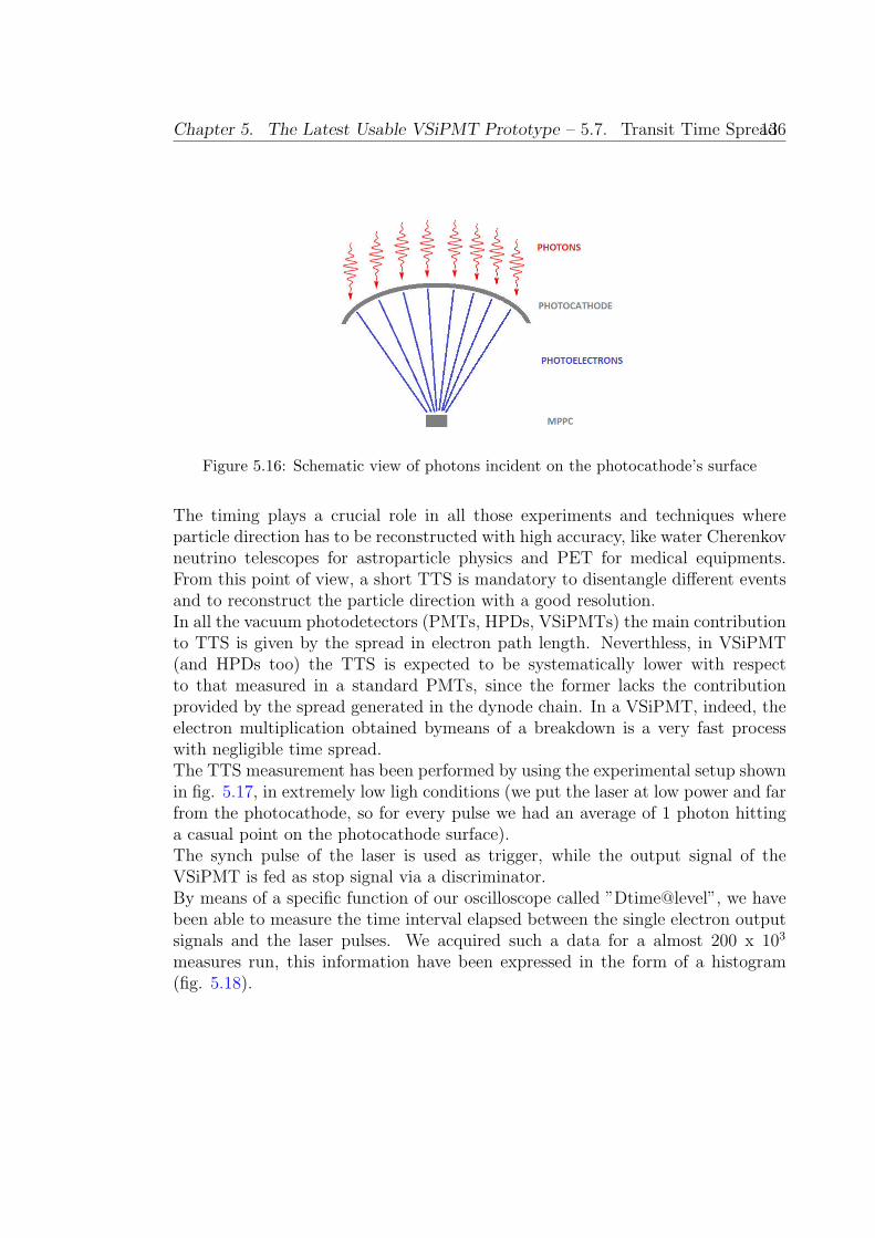
Chapter 5. The Latest Usable VSiPMT Prototype – 5.7. Transit Time Spread136
Figure 5.16: Schematic view of photons incident on the photocathode’s surface
The timing plays a crucial role in all those experiments and techniques whereparticle direction has to be reconstructed with high accuracy, like water Cherenkovneutrino telescopes for astroparticle physics and PET for medical equipments.From this point of view, a short TTS is mandatory to disentangle different eventsand to reconstruct the particle direction with a good resolution.In all the vacuum photodetectors (PMTs, HPDs, VSiPMTs) the main contributionto TTS is given by the spread in electron path length. Neverthless, in VSiPMT(and HPDs too) the TTS is expected to be systematically lower with respectto that measured in a standard PMTs, since the former lacks the contributionprovided by the spread generated in the dynode chain. In a VSiPMT, indeed, theelectron multiplication obtained bymeans of a breakdown is a very fast processwith negligible time spread.The TTS measurement has been performed by using the experimental setup shownin fig. 5.17, in extremely low ligh conditions (we put the laser at low power and farfrom the photocathode, so for every pulse we had an average of 1 photon hittinga casual point on the photocathode surface).The synch pulse of the laser is used as trigger, while the output signal of theVSiPMT is fed as stop signal via a discriminator.By means of a specific function of our oscilloscope called ”Dtime@level”, we havebeen able to measure the time interval elapsed between the single electron outputsignals and the laser pulses. We acquired such a data for a almost 200 x 103
measures run, this information have been expressed in the form of a histogram(fig. 5.18).
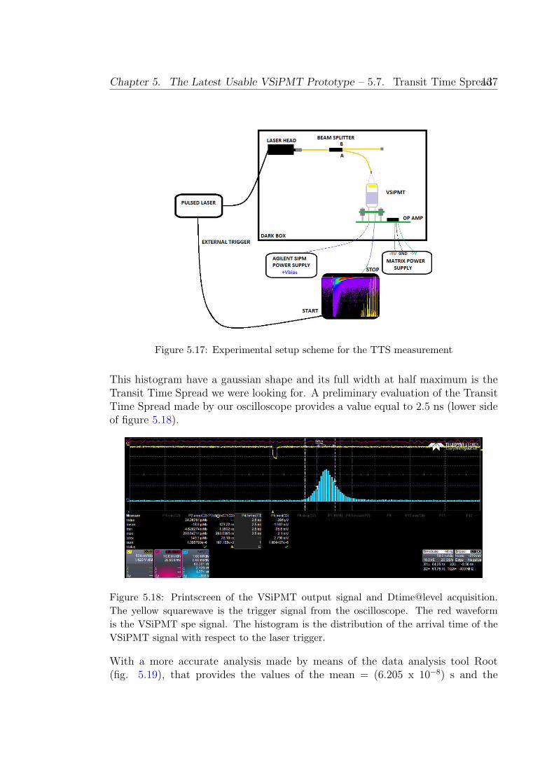
Chapter 5. The Latest Usable VSiPMT Prototype – 5.7. Transit Time Spread137
Figure 5.17: Experimental setup scheme for the TTS measurement
This histogram have a gaussian shape and its full width at half maximum is theTransit Time Spread we were looking for. A preliminary evaluation of the TransitTime Spread made by our oscilloscope provides a value equal to 2.5 ns (lower sideof figure 5.18).
Figure 5.18: Printscreen of the VSiPMT output signal and Dtime@level acquisition.
The yellow squarewave is the trigger signal from the oscilloscope. The red waveform
is the VSiPMT spe signal. The histogram is the distribution of the arrival time of the
VSiPMT signal with respect to the laser trigger.
With a more accurate analysis made by means of the data analysis tool Root(fig. 5.19), that provides the values of the mean = (6.205 x 10⁻⁸) s and the
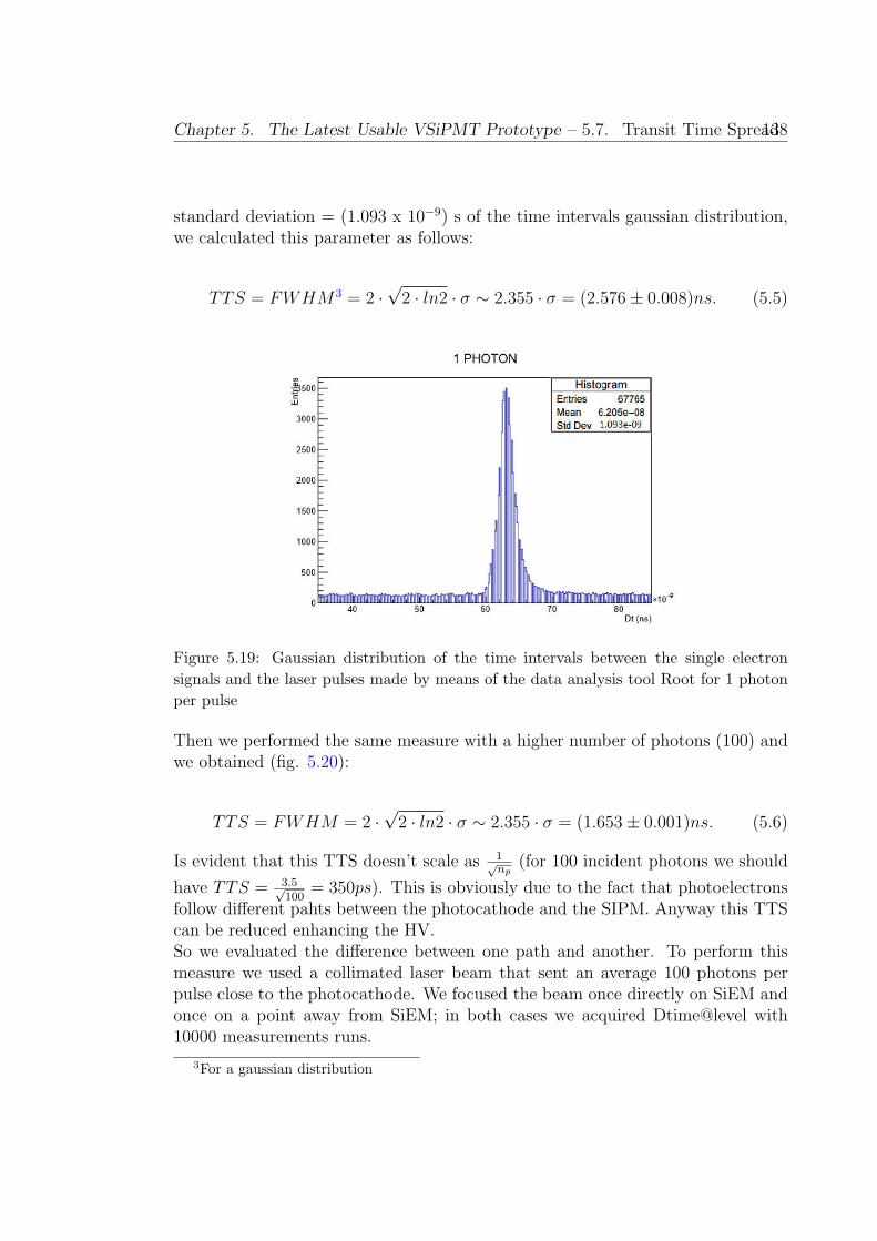
Chapter 5. The Latest Usable VSiPMT Prototype – 5.7. Transit Time Spread138
standard deviation = (1.093 x 10⁻⁹) s of the time intervals gaussian distribution,we calculated this parameter as follows:
TTS = FWHM3 = 2 ·√2 · ln2 · σ ∼ 2.355 · σ = (2.576± 0.008)ns. (5.5)
Figure 5.19: Gaussian distribution of the time intervals between the single electron
signals and the laser pulses made by means of the data analysis tool Root for 1 photon
per pulse
Then we performed the same measure with a higher number of photons (100) andwe obtained (fig. 5.20):
TTS = FWHM = 2 ·√2 · ln2 · σ ∼ 2.355 · σ = (1.653± 0.001)ns. (5.6)
Is evident that this TTS doesn’t scale as 1√np
(for 100 incident photons we should
have TTS = 3.5√100
= 350ps). This is obviously due to the fact that photoelectronsfollow different pahts between the photocathode and the SIPM. Anyway this TTScan be reduced enhancing the HV.So we evaluated the difference between one path and another. To perform thismeasure we used a collimated laser beam that sent an average 100 photons perpulse close to the photocathode. We focused the beam once directly on SiEM andonce on a point away from SiEM; in both cases we acquired Dtime@level with10000 measurements runs.
3For a gaussian distribution

Chapter 5. The Latest Usable VSiPMT Prototype – 5.7. Transit Time Spread139
Figure 5.20: Gaussian distribution of the time intervals between the single electron
signals and the laser pulses made by means of the data analysis tool Root for 100 photons
per pulse. The little bulge on the right side of the distribution is due to afterpulses
The difference between one path and another will be given by the difference be-tween the means of the two distributions (fig. 5.21):
Figure 5.21: Gaussian distribution of the time intervals between the single electron
signals and the laser pulses made by means of the data analysis tool Root in the two
cases. The little bulge on the right side of the two distributions is due to afterpulses

Chapter 5. The Latest Usable VSiPMT Prototype – 5.8. Focusing 140
From this analysis results:
Time Difference Between Paths = (1.7966± 0.0003)ns (5.7)
Since the differences between the paths of electrons which come from differentpoints of the photocathode are on the order of a nanosecond, in these conditionsthe TTS can not be reduced to a value lower than the nanosecond.
5.8 Focusing
The capability of focusing uniformly photoelectrons over the SiEM surface is acrucial feature for the good operation of the VSiPMT.
Figure 5.22: Focusing in a VSiPMT
The photocathode of the VSiPMT prototype has a circular shape. Therefore, tak-ing into account the axial symmetry of the electric field generated by the focusingring, an approximately circular photoelectron spot is reasonably expected.Referring to figure 5.22, a too strong focusing makes the photoelectron spot smallerthan the SiPM active surface. This solution is deleterious because a too squeezedphotoelectron spot means that a fraction of the SiPM pixels is not involved, thistherefore drastically reduces the linearity of the device.However, a too weak focusing causes a photoelectron spot larger than the SiPMsurface. This means that a fraction of the photoelectron is sistematically missed,thus implying a reduction of the photon detection efficiency of the device.An optimal focusing condition is achieved if the photoelectron beam spot is per-fectly inscribed in the SiPM square target. In this case, no more than the 85% of

Chapter 5. The Latest Usable VSiPMT Prototype – 5.8. Focusing 141
the total number of cells of the SiEM can be fired. This is the configuration thatexploits the maximum number of pixels leading to an optimized use of the device.To prove the focusing of our prototype, we have the targeted with a laser beamat maximum power available to ensure that the SiEM reached the saturation (fig.5.23).
Figure 5.23: Saturated SiEM signal. By varying the laser power, above a certain thresh-
old, the amplitude of this signal remains unchanged. This means that it has reached
saturation
The maximum number of cells we fired was obtained by dividing the average valueof the charge contained in the saturated signal to the charge contained in thesingle cell signal (these values have been acquired with their error), the result was900 ± 15 . This means that the optimum solution for the focusing has not beenreached. To have the optimum, we should have 700 fired cells, which correspond toa circular spot inscribed in the SiEM surface of 7.1 mm2 area and 1.5 mm diameter(fig. 5.24).
Figure 5.24: Optimum focusing in our VSiPMT prototype
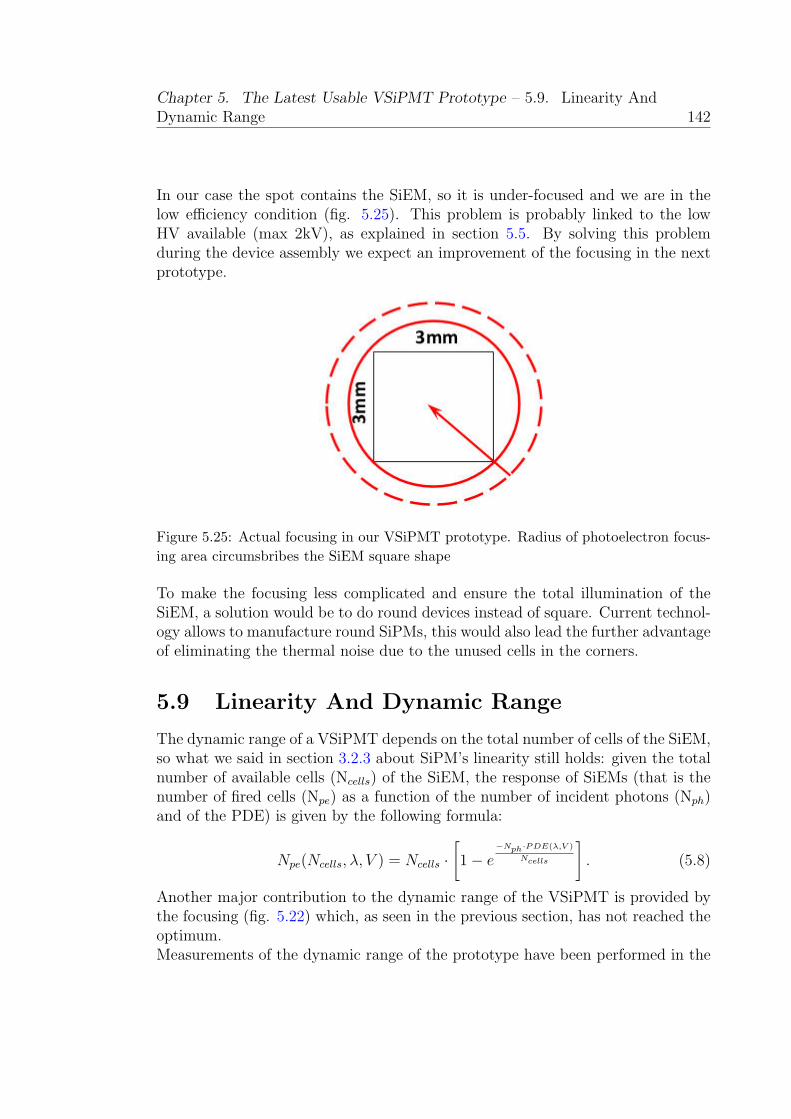
Chapter 5. The Latest Usable VSiPMT Prototype – 5.9. Linearity AndDynamic Range 142
In our case the spot contains the SiEM, so it is under-focused and we are in thelow efficiency condition (fig. 5.25). This problem is probably linked to the lowHV available (max 2kV), as explained in section 5.5. By solving this problemduring the device assembly we expect an improvement of the focusing in the nextprototype.
Figure 5.25: Actual focusing in our VSiPMT prototype. Radius of photoelectron focus-
ing area circumsbribes the SiEM square shape
To make the focusing less complicated and ensure the total illumination of theSiEM, a solution would be to do round devices instead of square. Current technol-ogy allows to manufacture round SiPMs, this would also lead the further advantageof eliminating the thermal noise due to the unused cells in the corners.
5.9 Linearity And Dynamic Range
The dynamic range of a VSiPMT depends on the total number of cells of the SiEM,so what we said in section 3.2.3 about SiPM’s linearity still holds: given the totalnumber of available cells (Ncells) of the SiEM, the response of SiEMs (that is thenumber of fired cells (Npe) as a function of the number of incident photons (Nph)and of the PDE) is given by the following formula:
Npe(Ncells, λ, V ) = Ncells ·[
1− e−Nph·PDE(λ,V )
Ncells
]
. (5.8)
Another major contribution to the dynamic range of the VSiPMT is provided bythe focusing (fig. 5.22) which, as seen in the previous section, has not reached theoptimum.Measurements of the dynamic range of the prototype have been performed in the

Chapter 5. The Latest Usable VSiPMT Prototype – 5.9. Linearity AndDynamic Range 143
same conditions and modality described in section 3.2.3 for a number of incidentphotons that goes from a maximum of 28777 to a minimum of 195 usign variousfilters (fig. 5.26). The experimental points are plotted in figure 5.27.
Figure 5.26: Experimental set up for dynamic range measurement
The graph in figure 5.27 shows the number of fired pixels versus the number ofincident photons (so the VSiPMT response).
Figure 5.27: Number of fired pixels as a function of the number of incident photons for
the VSiPMT prototype
The experimental data have been fitted with the following two parameters curve:

Chapter 5. The Latest Usable VSiPMT Prototype – 5.9. Linearity AndDynamic Range 144
y = a ·(
1− e−b·xa
)
, (5.9)
For ∼ 20000 incident photons the upper limit of the dynamic range has beenreached, the response of the VSiPMT begins to deviate from linearity and thesaturation occurs.The two parameters a and b provide the total number of the SiEM cells and totalphotodetection efficiency of the device:
a = Ncells = 945± 100 (5.10)
b = PDE = (2.77± 0.12)% (5.11)
The value of Ncells (the parameter a) is, within the error, equal to the total numberof the SiEM’s cells (900 as discussed above) as we expected. Since the total PDEresults to be ∼ 2% from the previous discussion, we see that the value of theparameter b is in agreement with the same value which comes out independentlyfrom other considerations.

Chapter 6
Conclusions and Perspects
In this thesis we performed a detailed characterization of the latest generationSiPMs in order to describe the current semiconductor detector’s technology stateof art with the final aim to choose the better core device for the realization ofthe next VSiPMT prototype. Moreover a further improvement has been proposedwith respect to the SiPMs characterized here.Then we performed a temperature characterization of a non so recent genera-tion SiPM in order to test the C11204-01 high-voltage power supply which is thesolution to SiPMs gain reduction with increasing temperature proposed by Hama-matsu. In the future it might be interesting to perform a similar study on theVSiPMT to achieve an amplification circuit which also includes the C11204-01high-voltage power supply; the aim should be to realize a even more compact de-vice with even less power consumption, since the C11204-01 requires just 5V powersupply to generate the voltage needed to supply the SiPM inside the VSiPMT (50to 90 V).Finally we performed an extensive characterization of the latest usable VSiPMTprototype. This analysis provided first-rate results: the VSiPMT offers very attrac-tive features and unprecedented performances, definitely superior to every otherphotodetector of the same sensitive surface.Negligible power cosumption, excellent SPE resolution, easy low-voltage-based sta-bility, very good time performances, high gain and wide dynamic range are amongthe most outstanding achievements, counterbalanced by few drawbacks like a stillhigh dark noise, a not so high PDE and a focus that has not yet reached theoptimum condition. However these are easily upgradeable design features whichcertainly will not appear again in the next prototypeIn this thesis are presented, for the first time ever, the results of tests performed ona novel technology manufactured by the world’s greatest photodetector company.A device which represents the truly usable realization of an idea born ten yearsago, with a sketch on a piece of paper.
145

Chapter 6. Conclusions and Perspects – 146
The development of this new detector has opened a new frontier in the field ofastroparticle physics, a field dominated for more than one century by PMT tech-nology. Even if new materials, new layouts and new solutions led to an incredibleimprovement of PMT performances, this technology suffers of some intrinsic draw-backs that strongly affect its performances, limiting its current field of applicationand even strongly compromising its secular leading role.By now the world of experimental physics is ready for the development of alter-native solutions to PMTs. Indeed, in the last decades, the strong developmentof silicon devices have boosted detector’s technology towards a new generationof solid-state photodetectors, passing through PIN photodiodes (with no inter-nal gain), Avalanche PhotoDiodes (APDs, operating in linear region with internalgains of up to a few hundreds) and avalanche photodiodes in Geiger-Mode (GAPDsor SiPMs, operating in Geiger regime with gains ranging between 105 and 106).These devices exhibit important advantages over PMTs, namely higher quantumefficiency, lower operation voltages (and hence strongly reduced power consump-tion), weak sensitivity to external magnetic fields, robustness and compactness.In particular, the SiPM technology, introduced in the first years of 21st century, hasknown a whirling evolution, that led current devices to reach an extremely chal-lenging level of performances, in terms of quantum efficiency, gain, photon countingcapabilities and time response. However, the small sensitive surface achieved bythe current generation of SiPMs (due mainly to thermal dark currents and Sili-con wafer costs) sets a strong limit to their possible field of application, makingthem weak photodetector candidates for most of the next generation astroparticlephysics experiments based on scintillation phenomena, Cherenkov or fluorescenceradiation.This is the framework in which the concept of VSiPMT was born. This solutionis expected to bring several important advantages in the comparison with stan-dard PMTs even because, while the PMT technology is not further improved,semiconductor’s technology is going through its golden age. The real impact ofsemiconductors on everyday people’s lives is huge, so research and development inthis area proceeds at a very high pace making potentially infinite improvements,which will involve the detectors that are based on this technology. Indeed, sinceHamamatsu already showed a great interest in the VSiPMT project and the relatedR&D path, could be interesting to arrange a consortium of european companies(PMT, SiPM and getters producers) to start a mass production for the next gen-eration of astroparticle physics experiments both in space and on heart.In conclusion, from the results that we have gathered, it is clear that this inventionis expected to represent a real breakthrough in the field of photodetectors, des-tined to revolutionize several research fileds (such as astroparticle physics, medicalapplications, material science and environment applications) and to change our

Chapter 6. Conclusions and Perspects – 147
way of seeing the world, which now appears with a higher resolution.

Appendix A
Lambertian Distribution
Lambertian reflectance is the property that defines an ideal ”matte” or diffuselyreflecting surface. The apparent brightness of a Lambertian surface to an observeris the same regardless of the observer’s angle of view. More technically, the sur-face’s luminance is isotropic, and the luminous intensity obeys Lambert’s cosinelaw: the radiant intensity or luminous intensity observed from an ideal diffuselyreflecting surface or ideal diffuse radiator is directly proportional to the cosine ofthe angle θ between the direction of the incident light and the surface normal [40].The situation for a Lambertian surface (emitting or scattering) is illustrated infigure A.1.
Figure A.1: Left: Emission rate (photons/s) in a normal and off-normal direction. The
number of photons/sec directed into any wedge is proportional to the area of the wedge.
Right: Observed intensity ( photonss·cm2·sr ) for a normal and off-normal observer; dA0 is the
area of the observing aperture and dΩ is the solid angle subtended by the aperture from
the viewpoint of the emitting area element.
We will think in terms of photons rather than energy or luminous energy. The
148

Appendix A. Lambertian Distribution – 149
wedges in the circle each represent an equal angle dΩ, and for a Lambertian surface,the number of photons per second emitted into each wedge is proportional to thearea of the wedge.It can be seen that the length of each wedge is the product of the diameter of thecircle and cos(θ). It can also be seen that the maximum rate of photon emissionper unit solid angle is along the normal and diminishes to zero for θ = 90. Inmathematical terms, the radiance along the normal is I · photons
s·cm2·sr and the numberof photons per second emitted into the vertical wedge is I · dΩ · dA. The numberof photons per second emitted into the wedge at angle θ is I · cos(θ) · dΩ · dA.Figure A.1 (right) represents what an observer sees. The observer directly abovethe area element will be seeing the scene through an aperture of area dA0 and thearea element dA will subtend a (solid) angle of dΩ0. We can assume without lossof generality that the aperture happens to subtend solid angle dΩ when ”viewed”from the emitting area element. This normal observer will then be recordingI · dΩdA photons per second and so will be measuring a radiance of:
I0 =I · dΩ · dAdΩ0 · dA0
· photons
s · cm2 · sr . (A.1)
The observer at angle θ to the normal will be seeing the scene through the sameaperture of area dA0 and the area element dA will subtend a (solid) angle ofdΩ0 · cos(θ). This observer will be recording I · cos(θ) ·dΩ ·dA photons per second,and so will be measuring a radiance of:
I0 =I · cos(θ) · dΩ · dAdΩ0 · cos(θ) · dA0
=I · dΩ · dAdΩ0 · dA0
· photons
s · cm2 · sr , (A.2)
which is the same as the normal observer.

Appendix B
Detection Efficiency of thePrevious VSiPMT PrototypesEB-MPPC050 (ZJ5025) andEB-MPPC100 (ZJ4991)
The fill factors of the SiPMs used for the ZJ5025 and the ZJ4991 prototypes are61% and 78%, respectively, and the quantum efficiency of the photocathode is 38%at λ = 407 nm. Taking into account these values, the expected PDE for the twoprototypes are PDEZJ5025 = 23% and PDEZJ4991 = 30%. The PDE with respectto the high voltage supplied to the photocathode has been measured with the sameprocedure described above and its behaviour is shown in figure B.1.PDE of the device becomes stable around ∼3 kV , with a plateau till ∼ 5 kV. The operating point for the high-voltage supply has been fixed to -3.2 kV ,corresponding to ∼ 23% PDE value, as we expected. Even lower operating pointscan be achieved by simply reducing the SiO2 layer of the SiEM. In this case thetotal efficiency at the plateau (where the trigger efficiency is effectively 1) has beencalculated as follows:
ǫtot = ǫPC · ǫgeom · ǫtrigger = 0.38 · 0.61 · 1 = 0.23 (B.1)
In these prototypes, unlike the EB-MPPC100 (XE2597) 1 INCH, the high voltageis able to drive photoelectrons to the SiEM surface and to give them the rightenergy to enter into the silicon bulk and produce the signal. Indeed if we calculatethe detection efficiency out of the plateau, we obtain:
ǫtot = ǫPC · ǫgeom · ǫtrigger = 0.38 · 0.61 · 0.39 = 0.09 (B.2)
150

Appendix B. Detection Efficiency of the Previous VSiPMT PrototypesEB-MPPC050 (ZJ5025) and EB-MPPC100 (ZJ4991) – 151
Figure B.1: Results of the photon detection efficiency test in function of the HV. The
PDE errors are obtained by the propagation of the errors on Npe and Nph.

Bibliography
[1] A. Einstein, Ann. Phys. 17 (1905) 132
[2] D. Renker, Geiger-mode avalanche photodiodes, history, properties and prob-lems, Nuclear Instruments and Methods in Physics Research A 567 (2006)48-56
[3] Saleh B. E., Teich M. C. Semiconductor photon detectors. Fundamentals ofPhotonics, pages 644, 695, 2007
[4] Miller S. Ionization rates for holes and electrons in silicon. Physical Review,105(4):1246, 1957
[5] K. Seeger, Semiconductor Physics, Springer-Verlag (1973)
[6] W. B. Burford III, H. Grey Verner, Semiconductor Junctions and Devices,McGraw-Hill (1965)
[7] S. O. Kasap, Optoelectronics and Photonics: Principles and Practices,Prentice-Hall (2001)
[8] J. Singh, Electronic and Optoelectronic Properties of Semiconductor Struc-tures, Cambridge University Press (2003)
[9] J. Millman, Circuiti e Sistemi Microelettronici, Bollati Boringhieri (1985)
[10] R. A. Greiner, Semiconductor Devices and Applications, McGraw-Hill (1961)
[11] G. F. Knoll, Radiation Detection and Measurement (3 ed.), John Wiley andSons (2000)
[12] W.R. Leo, Techniques for Nuclear and Particle Physics Experiments,Springer-Verlag (1987)
[13] K. G. McKay, Avalanche Breakdown in Silicon, Phys. Rev. 94, 877 (1954)
[14] R. J. McIntyre, Theory of Microplasma Instability in Silicon, J. Appl. Phys.32, 983 (1961)
[15] U. Marini, B. Marconi, A. Puglisi, L. Rondoni, A. Vulpiani, Fluctuation-Dissipation: Response Theory in Statistical Physics, Physics Reports vol.461, p. 111 (2008)
152

Bibliography – Bibliography 153
[16] Hamamatsu Photonics K., et al. Opto-semiconductor handbook
[17] Simon, Hermann (June 10, 2009), Hidden Champions of the Twenty-FirstCentury: The Success Strategies of Unknown World Market Leaders, Lon-don: Springer Science, Business Media.
[18] Avalanche photodiode, a user guide, understanding avalanche photodiode forimproving system performance
[19] McKay K., McAfee K. Electron multiplication in silicon and germanium.Physical Review, 1953.
[20] G. Barbarino, F. C. T. Barbato, et al., A new generation photodetector forastroparticle physics: The VSiPMT, Astroparticle Physics 67, July 2014
[21] Winston R., O’Gallagher J. Nonimaging concentrators (optics). In Meyers R.A., editor, Encyclopedia of Physical Science and Technology (Third Edition),pages 507 - 522. Academic Press, New York, third edition edition, 2003
[22] Piemonte C. Sipm technology at fbk. IPRD10, Siena, 2010.
[23] BARBARINO G. Single-photons count device based on photocathode andgeiger solid-state technology for the multiplication of photoelectrons, Jan-uary 15 2015
[24] Barbarino G., De Asmundis R., De Rosa G., Fiorillo G., Gallo V., Russo S.,A new high-gain vacuum photomultiplier based upon the amplification ofa geiger-mode p-n junction. Nuclear Instruments and Methods in PhysicsResearch Section A: Accelerators, Spectrometers, Detectors and AssociatedEquipment, 594(3): 326-331, 2008
[25] Sommer A. H. Brief history of photoemissive materials. In SPIE’s 1993 Inter-national Symposium on Optics, Imaging, and Instrumentation, pages 2-17.International Society for Optics and Photonics, 1993
[26] Spicer W. E., Herrera-Gomez A. Modern theory and applications of photo-cathodes. In SPIE’s 1993 International Symposium on Optics, Imaging, andInstrumentation, pages 18-35. International Society for Optics and Photon-ics, 1993
[27] Spicer W. Negative affinity 3-5 photocathodes: Their physics and technology.Applied physics, 12(2):115-30, 1977
[28] Sommer A. H. Photoemissive materials. preperation, properties and uses.Huntington: Krieger, 1980, 1, 1980
[29] G. Barbarino, F. C. T. Barbato et al: Vacuum Silicon PhotoMultipliers: re-cent developments. Nuclear Instruments and Methods in Physics ResearchSection A: Accelerators, Spectrometers, Detectors and Associated Equip-ment, 718: 582-583, 2013
Bibliography – Bibliography 154
[30] C. Piemonte, A. Ferri, A. Gola, A. Picciotto, T. Pro, N. Serra, A. Tarolli,N. Zorzi, Development of an automatic procedure for the characterization ofsilicon photomultipliers, Conference Record of NSS/MIC 2012, IEEE, 2012
[31] S. Sze and K. Ng, Physics of Semiconductor Devices, 3rd ed. Hoboken, NJ:Wiley-Interscience, 2006
[32] N. Serra, A. Ferri, A. Gola, T. Pro, A. Tarolli, N. Zorzi, C. Piemonte, Charac-terization of new FBK SiPM technology for visible light detection, in ”JOUR-NAL OF INSTRUMENTATION”, vol. 8, n. P03019, 2013
[33] Hamamatsu SiPM Multi Pixel Photon Counters S10931-100P seriesdatasheet, september 2010
[34] C. Piemonte, A. Ferri, A. Gola, T. Pro, N. Serra, A. Tarolli, N. Zorzi, Charac-terization of the First FBK HighDensity Cell Silicon Photomultiplier Tech-nology, in ”IEEE TRANSACTIONS ON ELECTRON DEVICES”, vol. 60,n. 8 2013
[35] M. Grodzicka, Member, IEEE, M. Moszynski, Fellow, IEEE, T. Szczesniak,Member, IEEE, M. Szawlowski, D. Wolski , K. Lesniewski, Effective deadtime of APD cells of SiPM IEEE Nuclear Science Symposium ConferenceRecord, 2011
[36] M.Grodzicka, M. Moszynski, T. Szczesniak, M. Szawlowski, D. Wolski,J. Baszak. ”2x2 SiPM Arrays in Gamma spectrometry with CsI(Tl),LSO:Ce(Ca), LaBr3, BGO” in IEEE Nuclear Science Symp. Conf. Rec.,Valencia, CF, Oct. 2011
[37] N. Akil, S. E. Kerns, D. V. Kerns, Jr., A. Hoffmann, and Jean-Pierre Charles,”A Multimechanism Model for Photon Generation by Silicon Junctions inAvalanche Breakdown” IEEE Trans. on Electron Devices vol. 46, No. 5(1999)
[38] Power Supply module for SiPM C11204-01, Operation Manual
[39] Power Supply module for SiPM C11204-01, Command Reference
[40] Modern Optical Engineering, Warren J. Smith, McGraw-Hill
[41] Barbarino G. et al., Proof of feasibility of the Vacuum Silicon PhotoMultiplierTube (VSiPMT), Journal of Instrumentation, Volume 8, Issue 04, article id.P04021 (2013)
[42] Barbarino G., Barbato F. C. T. et al., A new generation photodetector forastroparticle physics: The VSiPMT, Astroparticle Physics, Volume 67, p.18-25, 2015
[43] Engstrom R. et al. Rca photomultiplier manual. RCA Electronic Components,Harrison, NJ, 1970
Ringraziamenti
Quando mi sono laureata alla triennale avrei dovuto scrivere i ringraziamenti nellatesi ma non l’ho fatto, perche ero immatura, perche ero delusa... Ho sbagliato.C’erano tantissime persone che avrebbero meritato di essere rigraziate, perche og-nuna di loro ha contribuito a suo modo alla mia crescita come persona e comescienziato. Stavolta non commettero lo stesso errore, a queste persone dedicol’ultimo capitolo della mia tesi magistrale, il culmine di un perscorso durato anni,che mi ha reso la persona che sono.Il primo e piu importante ringraziamento va fatto al Professor Barbarino, che miha accolto nel suo gruppo di ricerca e mi ha coinvolto nel suo progetto piu bello,che ha sempre creduto in me dandomi la possibilita di confrontarmi con la realehard research e che mi ha gratificato con la sua stima e la sua fiducia.Ringrazio la Dottoressa Barbato, Felicia, che e stata dal primo momento il miopunto di riferimento, oltre che un’amica e un supporto nei momenti di difficolta.Senza di lei non sarei stata in grado nemmeno di mettere piede in un laboratorio.Ringrazio Antonio (Vanzanella), Nicola e Marco per la loro squisita disponibilitae validissima competenza elettronica. Il successo nella stesura di questa tesi e ingrossa parte anche merito loro.Ringrazio inoltre il Professor Guarino per i suoi consigli, il Dottor de Asmundis perle consulenze LabView, il Dottor Di Capua, il Professor Campajola, la DottoressaDe Rosa, il Dottor Mollo e il Dottor Vivolo per l’aiuto che mi hanno dato.Un percorso come questo non si esaurisce nel solo lavoro di tesi. La tesi e solol’ultimo di una serie di ostacoli che ognuno di noi deve superare per crescere. Eimpensabile affrontare queste difficolta da soli, per cui i miei sentiti ringraziamentivanno a coloro che mi hanno accompagnato nel mio percorso e che mi hanno aiu-tato a superarle, a coloro che hanno gioito con me dei miei successi, che mi hannoincoraggiato nei miei fallimenti, che sono stati in ansia per me quando dovevo af-frontare prove difficili e che ci sono sempre stati.A mia madre e mio padre, che con i loro sacrifici mi hanno dato la possibilita diarrivare fino a questo punto, a mio fratello Giovanni e a Nunzia, che mi hanno datoil loro sostegno incondizionato in ogni momento e a mia sorella Ludovica, per tuttigli abbraccini, che non sempre ho ricambiato. Il conforto delle nostre chiacchiere
155
Bibliography – Bibliography 156
a tavola mi ha dato spesso la forza di andare avanti e superare anche i momentipiu bui.A nonno Umberto e nonna Maria, che mi hanno insegnato la dedizione al lavoro ela tenacia, le due qualita su cui ho basato il mio intero percorso universitario.A Italo, Rosaria, Diego ed Emanuela che mi hanno accolta in casa loro con calore,e mi amano come un membro della famiglia.Al mio Maestro Sergio e alle mie ballerine Maria, MariaPia, Francesca e Diana,perche senza di voi e senza la danza i problemi sarebbero sembrati piu grandi e lavita piu triste.L’universita e una fase transitoria della vita, una fase che si esaurisce in fretta,ma alcuni dei legami che si creano in questo frangente sono destinati a durare. Unringraziamento affettuoso va quindi ai miei colleghi, che hanno visto da vicino lamia evoluzione e mi hanno dimostrato in molte occasioni il bene che mi vogliono.A Giulia, per essere, senza saperlo, un esempio di grande forza per me; ad Anna,per essermi stata vicina in un momento molto delicato; a quella pazza della Fiore,per aver messo le mani nel ciaccio insieme a me; a Fabio (Mele) per la nostra gagdella finestra; a Federica, per aver condiviso con me l’ansia da Santorelli; a Mariaper tutte le nostre chiacchierate da corridoio; a Davide, perche senza il suo aiutoun intero capitolo di questa tesi non sarebbe stato scritto; a Mario, che ha placatola mia ansia interrogandomi prima di svariati esami, e a Vincenzo che cosı si e fattouna cultura di elettronica; a Mariano, a cui chiedero senza dubbio di organizzareil mio matrimonio; a Luca (Buonocore), per tutto l’affetto che mi ha sempre di-mostrato; a Fabio (Formisello) e Giovanni, per quell’epica maratona del Signoredegli Anelli, per il Jazz e per tutti i discorsi da ora del te; a Luca (Tortorelli),per quell’indimenticabile mattinata all’Osservatorio di Capodimonte; a Martina eCarmen, le mie particellari preferite; a Giorgio, Daniele, Felice e Mauro, per tuttii discorsi da ora di pranzo (quelli seri e quelli meno seri); a Fiammetta, Pierpaolo,Silvia, Lollo e Antonio (Bellotta), per tutti i consigli e il sostegno che non mihanno mai fatto mancare, anche a distanza; al Principe, per tutte le risate, le cenemessicane, i ribaltamenti e i giovedı misogini; a Sandrone, per essere sempre ecomunque il mio migliore amico.Dulcis in fundo, il mio ringraziamento piu vivo va ad una delle persone piu straordi-narie che abbia avuto la fortuna di incontrare, alla persona che ha dato il maggiorecontributo alla mia carriera, alla persona che ho scelto come compagno di vita.A Marco, perche da quando ci sei tu io non mi sento mai sola; perche mi haiincoraggiato fino a farmi prendere coscienza delle mie reali potenzialita; per tuttol’aiuto e il supporto concreto che mi hai dato, senza il quale non avrei fatto unacarriera magistrale cosı brillante; perche hai reso la mia vita migliore.