the resistance and strength of soft solder splices …mice.iit.edu/mnp/mice0308.pdfsolders be...
TRANSCRIPT

MICE Note 308
1
Abstract— Two of the three types of MICE magnets will have
splices within their coils. The MICE coupling coils may have as many as fifteen one-meter long splices within them. Each of the MICE focusing coils may have a couple of 0.25-meter long conductor splices. Equations for the calculation of resistance of soldered lap splices of various types are presented. This paper presents resistance measurements of soldered lap splices of various lengths. Measured splice resistance is shown for one-meter long splices as a function of the fabrication method. Another important consideration is the strength of the splices. The measured breaking stress of splices of various lengths is presented in this paper. Tin-lead solders and tin-silver solders were used for the splices that were tested. From the data given in this report, the authors recommend that the use of lead free solders be avoided for low temperature coils.
Index Terms—Splice Resistance, Splice Strength.
I. INTRODUCTION PLICES are common occurrence in superconducting magnets of all types [1]. Splices fall into two general
categories superconducting splices and normal splices. Magnets that must run in persistent mode generally have splices that are superconducting. Normal splices involve connecting the normal stabilizer metal of one conductor with the normal metal of the second conductor. In a normal splice the current flow from the superconductor of the first conductor through normal metal to the superconductor of the second conductor. This paper discusses normal splices between conductors that can be wound into a superconducting coil.
The magnets for the muon ionization cooling experiment (MICE) [2] cooling channel are a case in point. Two types of these coils contain splices because the available conductor piece lengths are too short. Because the coil currents are low (<300 A) and the splices are not cooled with helium directly, the splice resistance must also be low (<10 nΩ). MICE coil splices must have the following characteristics; 1) the splice must be less than one turn length, 2) the longitudinal or radial space occupied by an insulated splice must be less than the space occupied by two turns within the coil.
Manuscript received 3 August 2010. This work was supported by funds of
the cryogenic and superconductivity technology innovation project under the “985-2” plan of Harbin Institute of Technology. This work was also supported by the Office of Science, United States Department of Energy under contract DE-AC-02-05CH11231.
H. Wu, H. Pan, F. Y. Xu, X. K. Liu, and S. X. Zheng are with the Institute of Cryogenics and Superconductive Technology, HIT, Harbin 150001, China. L. Wang, is with the Shanghai Institute of Applied Physics, Shanghai 201204, China. M. A. Green is with Lawrence Berkeley National Laboratory, Berkeley CA, 94720 USA (e-mail: [email protected]). D. Diederich, T. Gartner, H. Higley, M. Mentik D. Tam, and F. Trillaud are also with LBNL.
Cold Welded Butt Splice
Soft Soldered Lap Splice
Up-down Lap Splice(Layer-to-layer Splice)
Side-by-side Lap Splice(within a Layer Splice)
L
Fig. 1. Cold-welded butt splice and two types of lap splices.
Fig. 1 shows the three types of normal splices were studied;
cold welded butt splices, soldered up-down lap splices, and soldered side-by-side lap splices [3], [4]. The fabricators for the coupling magnet [5] and the AFC magnet [6] have chosen to make their splices at the ends of a layer, so that the splice is a transition from one layer to the next. Therefore, the measurements presented here are for up-down soldered lap splices, which can be used at the ends of a coil layer.
II. CALCULATION OF SPLICE PARAMETERS
A. Calculation of the Splice Resistance The resistance for a butt splice can be expressed as follows:
€
R j =ρ jLJAcj
(r +1)r
(1)
where Rj is the resistance of the splice; ρj is the electrical resistivity of the weld material in the splice; Lj is the length of the fused region within the splice; r is the conductor copper to S/C ratio; and Acj is the conductor cross-sectional area. For a MICE conductor butt splice, ρJ = 1.6x10⁻⁹ Ωm, Lj = 100 µm, and Acj = 1.5x10⁻⁶ m2. The calculated resistance of this splice is 106 nΩ, which is too high for MICE magnets [7].
The calculated resistance of a lap splice of length L is divided into two terms, the copper resistance and the solder resistance. The un-insulated MICE coupling coil conductor has a width w = 1.6 mm and a thickness t = 0.95 mm. The coupling coil conductor has rounded corner Rc = 0.2 mm. The resistance of up-down lap splices is given as follows:
€
R j =2ρCutCu
L(w − 2Rc )+
ρsol tsolL(w − 2Rc )
(2)
The Resistance and Strength of Soft Solder Splices between Conductors in MICE Coils
H. Wu, H. Pan, M. A. Green Member IEEE, D. Dietderich Member IEEE, T. E. Gartner, H. C. Higley, M. Mentink, D. G. Tam, F. Y. Xu, F. Trillaud, X. K. Liu, L. Wang, and S. X. Zheng
S
MICE Note 308
2
The resistance for side-by-side lap splices is as follows:
€
R j =2ρCutCuL(t − 2Rc )
+ρsol tsol
L(t − 2Rc ) (3)
where ρCu is the copper resistivity; ρsol is the solder resistivity; tCu is the copper thickness; and tsol is the solder thickness. The coupling magnet the field at a splice is about 5 T. At 5 T, ρCu = 4.63x10⁻¹⁰ Ωm (RRR = 70 Cu) [8] and ρsol = 5.74x10⁻⁹ Ωm (tin-lead eutectic solder) [9]. A coupling coil splice L = 1 m, tCu = 150 µm, and tsol = 100 µm. For an up-down splice the calculated resistance is 0.58 nΩ. For a side-by side splice the calculated resistance is 1.37 nΩ. (At 0 T, the splice resistance is ~15 percent lower.)
The equations above assume that there is no solder in the space between the corners. Without rounded corners, the splice resistance is lower. The equations also assume that there is complete solder coverage within the splice. The equations should be considered to be approximate. They don’t consider a number of effects such as the alloying of the solder with the conductor copper, Hall effects in the splice, or the effects of current distribution in the conductor. The MICE conductor has a Cu to S/C ratio of 4. There are 222 filaments twisted with a pitch of 19 mm. Since the conductor is small, the current redistribution time is short. Splices between cables will have much longer current redistribution time constants.
B. Calculation of Splice Breaking Strength Short splices fail in shear within the splice solder. Long
splices fail in the parent material through a combination of pure tensile stress and bending stress that is induced by the distance between the conductor centers t/L. Thus short splices that are too long to fail in shear will fail at a lower tensile stress in the conductor than an infinitely long splice. The failure will occur where the bending stress is the highest (at a point right next to the splice). This kind of failure was observed in all of the 293 K splices that were in tension.
For short splices that fail within the splice due to shear in the solder, the tensile failure stress should be proportional to the splice length, unless bending induces brittle peeling within the splice itself. The shear failure stress for a typical soft solder at room temperature is from 20 to 35 MPa depending on the solder and the bond quality. The length below which shear failure occurs Lsf can be estimated as follows:
€
Lsf ≈σ ultτ sol
t , for up-down splices, and (4)
€
Lsf ≈σ ultτ sol
w , for side-by-side splices, (5)
where σult is the ultimate stress for the parent conductor in tension and τsol is the solder shear failure stress.
For a coil conductor w = 1.6 mm and t = 0.95 mm, the length Lsf, at which shear failure become dominant will be from 13 mm to 24 mm for an up-down splice. For a side-by-side splice, Lsf, will be from 21 mm to 38 mm. The coil splice length should be long compared to Lsf (>250 mm).
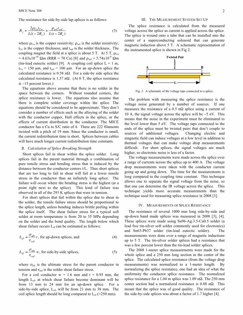
III. THE MEASUREMENT SYSTEM SET UP The splice resistance is calculated from the measured
voltage across the splice as current is applied across the splice. The splice is wound onto a tube that can be installed into the center of a superconducting solenoid that can generate magnetic induction above 5 T. A schematic representation of the instrumented splice is shown in Fig 2.
L
A B
Twisted Pair
Fig. 2. A schematic of the voltage taps connected to a splice.
The problem with measuring the splice resistance is the
voltage noise generated by a number of sources. If one measures the resistance of a 0.5 nΩ splice using a current of 10 A, the signal voltage across the splice will be ~5 nV. This means that the noise in the experiment must be eliminated to the level lower than 5 nV. The voltage taps connected to the ends of the splice must be twisted pairs that don’t couple to sources of additional voltages. Changing electric and magnetic field can induce voltages at a low level in addition to thermal voltages that can make voltage drop measurements difficult. For short splices, the signal voltages are much higher, so electronic noise is less of a factor.
The voltage measurements were made across the splice over a range of currents across the splice up to 400 A. The voltage drop measurements were taken with the conductor current going up and going down. The time for the measurements is long compared to the coupling time constant. This technique allows one to separate the signal voltage from the noise, so that one can determine the IR voltage across the splice. This technique yields more accurate measurements than the technique used for measuring splice resistance in 2008 [3].
IV. MEASUREMENTS OF SPLICE RESISTANCE The resistance of several 1000 mm long side-by-side and
up-down hand made splices was measured in 2008 [3], [4]. These splices were made using Sn96-Ag.3.5-Cu0.5 solder (a lead free tin-silver soft solder commonly used for electronics) and Sn63-Pb37 solder (tin-lead eutectic solder). The measurements were done over a range of magnetic inductions up to 5 T. The tin-silver solder splices had a resistance that was a few percent lower than the tin-lead solder splices.
The 2008 1-meter splice measurements were made for the whole splice and a 250 mm long section in the center of the splice. The calculated splice resistance (from the voltage drop measurements) was normalized to a 1-meter length. By normalizing the splice resistance, one had an idea of what the uniformity the conductor splice resistance. The normalized splice resistance for a 1.04 m splice was 1.09 nΩ. The 250 mm center section had a normalized resistance is 0.88 nΩ. This meant that the splice was of good quality. The resistance of the side-by-side splices was about a factor of 1.7 higher [4].

MICE Note 308
3
Fig. 3 shows the resistance of up-down splices as a function of their length at inductions of 0, 3T, and 5T using MICE coupling coil superconductor (0.95 mm by 1.60 mm) and Sn63-Pb37 (tin-lead eutectic) solder. The splices measured for Fig 3 were made using a jig to compress the splice so the solder thickness was reduced.
100010010.1
1
10
B = 0 TB = 3 TB = 5 T
Splice Length (mm)
Splic
e R
esist
ance
(n-o
hm)
Fig. 3. The splice resistance as a function of splice length and magnetic induction for up-down Splices using 0.95 by 1.60 mm Bare conductor and an Sn63-Pb37 (tin-lead eutectic solder with a melting point of 188 C).
From Fig. 3, it appears that the splice resistance is inversely proportional to the splice length until the splice length reaches 1-meter. The measured 1-meter long splice resistance at B = 0 appears to be inversely proportional to splice length. The 1-meter long splice resistance measurements at 3 T and 5 T appear to be too high. There has been considerable discussion as to why the 1-meter long splice resistance is different from the data for shorter splices. The differences are likely to be tied to the techniques used to eliminate noise from the splice voltage drop measurements. We don’t think dB/dt is a factor.
It also appears that the splices made using a jig have a lower resistance than splices made my hand using hemostats as clamps. This statement may not be true, based on the measured solder thickness for both types of splices. There is not much difference in the solder thickness for the splices made using a jig. The observed differences in the measured resistance may be due to improvements in the measurement technique that was used for the jig-fabricated samples. The resistance measurement method used in 2010 appears to have a lower noise level than the method used in 2008.
V. MEASUREMENTS OF SPLICE BREAKING STRENGTH A series of measurements of the breaking strength in
tension were done on a number of 250-mm long splices. These measurements were done on splices with the Sn96-Ag3.5-Cu0.5 (Sn-Ag) solder and on splice samples made from Sn63-Pb37 (Sn-Pb eutectic) solder. Splices were broken with the splices at 293 K and at 77 K. In the case of the 77 K samples, the splices themselves were at 77 K while the conductor at the ends of the sample was at 293 K.
All of the 293 K samples broke in the conductor right next to splice, which indicates that there is a stress concentration at that location. We believe that the stress concentration is due to conductor bending stress right next to the splice. The
bending stress is added to the tensile stress in the material on one side of the conductor. We also believe that this bending stress is a function of t/L where t is the thickness of the conductor and L is the length of the splice. All of the splices that were at 77 K broke at the sample end near room temperature. The ultimate tensile stress for the bare conductor is much higher at 77 K that it is at 293 K. None of the 250-mm long splices broke in the splice itself.
Fig. 4. Peel in a splice made with Sn-Ag solder broken at 77 K.
Most of the 250 mm long splices broken at 77 K exhibited
peeling of one conductor in the splice from the other. The length of the peel zone varied from 5 mm to 120 mm. Fig. 4 shows the peel in a splice made with Sn-Ag solder broken at 77 K. All of the Sn-Ag solder samples broken at 77 K exhibited peel. One splice made with Sn-Pb solder exhibited no peel at 77 K. The other Sn-Pb splice had a 5 mm long peel. We believe that the brittleness of the Sn-Ag solder at cryogenic temperature contributes to the peel exhibited in the 250 mm long splices measured at 77 K. Another contributing facto may be the bending of the conductor at the splice.
The peel phenomena and the apparent stress concentration next to the splice caused us to investigate the breaking strength of splices that were shorter than 250 mm. Fig. 5 shows the breaking stress for soldered up-down splices of various lengths and solders. The breaking stress in Fig. 5 is based on the parent conductor, which has a cross-section area of 1.485 mm2. All of the splices were stressed in tension.
1000100100
100
200
300
400
500
600
Sn-Pb (293 K)Sn-Pb (77 K)Sn-Ag (293 K)Sn-Ag (77 K)Sn-Pb (77 K) SpliceSn-Ag (77 K) Splice
Splice Length (mm)
Brea
king
Str
ess i
n th
e Pa
rent
Mat
eria
l (M
Pa)
Breaking Stress Limits for the Bare Conductor
Fig. 5. The breaking stress of splices of various lengths.

MICE Note 308
4
The two horizontal lines in Fig. 5 represent the upper and lower limits of the breaking stress for the bare superconductor without a splice. The breaking stress of most of the 230 to 270 mm splices lie within the range of the breaking stress for the conductor without a splice. The cases represented by closed and open triangles are cases where the splice broke apart during the break test. Splices made from the tin-silver solder are particularly prone to splice breakage at 77 K. For the tin lead eutectic solders only the shortest (~25 mm long) splices broke within the splice.
It is clear that the tin-silver solder is more prone to breakage than splices made with the tin-lead eutectic solder. In general, the splice breaking stress decreases as the splice gets shorter. The tin-silver solder doesn’t appear to be as strong as tin-lead solder, for splice lengths less than 250 mm. In the shorter splices, there is combination of peel and shear failure within the samples. All of the tin-silver solder splices peeled when they broke at 77 K. The tin-lead eutectic splices were far less likely to peel. Fig. 6 shows a hand made tin-silver solder splice that had been stressed, but hadn’t failed within the splice. One can see that the solder in the splice is cracked.
Fig. 6. A cross-section of a cracked Sn-Ag up-down splice after it broke. (Note the solder thickness in the splice before the spice cracked appears to be less than 50 µm. One can see the Nb-Ti filaments within the Cu matrix.)
VI. CONCLUSIONS. There are a number of conclusions that can be drawn from
the splice measurements that have been made to date. From the measurements we find the following: 1) The splice length should be at least ten times the length at which the splice will fail due to shear failure in the solder. We believe that longer splices also reduce the effects of bending stress in the conductor. 2) Splices must be mechanically supported. Do not depend on the solder to keep the splice from coming apart. 3) The tin-silver solders (favored by those who want to get the lead out of solder) should be avoided. Tin-silver solders commonly used for room temperature electronics are very
brittle at temperatures less than 150 K [10]. Pure tin as a solder should also be avoided, because of a low temperature phase change that occurs in tin. The low temperature properties of lead-free solders must be well understood before these solders are used for making conductor splices for use at low temperatures.
In addition the authors of this paper make the following general recommendations concerning splices: 1) The melting point of the highest melting point solder in the splice must be less than the temperature that spoils the heat treatment of the superconductor. For Nb-Ti, this is < 250 C for a few minutes. 2) Splices made with two solder joints must have solders with different melting point temperatures in the joints. The part of the splice made first (usually between two superconductors) must be soldered together using the higher melting point solder (a solder with more lead). The second part of the splice (usually copper around a conductor) should be soldered using a lower melting point solder (such as tin-lead eutectic). In this instance careful temperature control is needed to keep the higher temperature solder from melting while the lower temperature parts of the splice are being fabricated. 3) Splices should be inspected before they are sealed into a coil or a magnet cryostat. This means that inspection criteria must be developed and implemented.
REFERENCES [1] C. A. Baldan, U. R. Oliveira, C. Y. Shigue, and E. R. Filho, “Evaluation
of Electrical Properties of Lap Joints for BSCCO and YBCO Tapes,” IEEE Transactions on Applied Superconductivity 19, No. 3, p 2831, (2009).
[2] G. Gregoire, G. Ryckewaert, L. Chevalier, et al, “MICE and International Muon Ionization Experiment Technical Reference Document,” http://www.mice.iit.edu, 2001.
[3] M. A. Green, D. Dieterich, H.C. Higley, et al, “The Calculated and Measured Resistance for Splices between Conductors in a MICE Superconducting Coil,” MICE Note 238, http://www.mice.iit.edu.
[4] F. Y. Xu, H. Pan, H. Wu, et al, “Measurement of Resistance and Strength of Conductor Splices in the MICE Coupling Magnets,” to be published in Advances in Cryogenic Engineering 55, AIP Press, Melville NY (2010).
[5] L. Wang, F. Y. Xu, H. Wu, et al, “Magnetic and Cryogenic Design of the MICE Coupling Solenoid Magnet System,” IEEE Transactions on Applied Superconductivity 19, No. 3, p 1344 (2009), MICE Note 234, http://www.mice.iit.edu.
[6] D. E. Baynham, T. W. Bradshaw, J. H. Cobb, et al, “Progress on the Design and Fabrication of the MICE Focusing Magnets,” to be published in IEEE Transactions on Applied Superconductivity 20, No. 3, (this publication) (2010).
[7] X. L. Gou, Harbin Institute of Technology, private communication concerning the 25-nohm resistance of 6-mm2 cross-section area butt splice.
[8] Handbook of Materials for Superconducting Machinery, Metal and Ceramics Information Center, MIC-MB-04, National Bureau of Standards, January 1977.
[9] F. Heringhaus and T. A. Painter, “Magnetoresistance of Selected Sn and Pb based solders at 4.2 K,” Materials Letters 57, Issue 4, pp 787-793, Elsevier BV (2002).
[10] Phil Eckels General Electric (retired) private communication concerning the fracture toughness data for tin-silver solders at low temperature.