the para80set - qrpguys
TRANSCRIPT

The Para80set
Designed by Steve, KD1JV -- Distributed by the QRP Guys
The “Para80set” is an updated version of the MAS80, which originally designed by Steve, KD1JV for the M.A.S. design contest (minimum art session), a contest started by Dr. Harmut "Hal" Weber, DJ7ST. (Now a SK). The idea behind this contest is to encourage Hams to build and operate a rig using a minimal number of parts. Steve has made some improvements and modifications and the result is the Para80set. It is named to commemorate the “Paraset” clandestine vacuum tube transceiver that was parachuted behind enemy lines to Allied resistance groups in northern Europe, and Scandinavia during WW II.
This new design still incorporates a sensitive regenerative receiver and a 3 watt, 80m crystal controlled CW transmitter, like the original “Paraset”, but with modern solid state components. The improvements over the original MAS80 design include a more efficient transmitter and a “spot” switch to locate the transmit frequency in the receiver, along with a 2 crystal switch option. Some component values have been tweaked to reduce the number of different part values and provide better high frequency roll off of the audio.
Specifications:
Supply voltage range: 12V to 13.8V
Receiver:
Current: ~ 20 maSensitivity: ~ 0.5 uV MDSMain tuning range: ~ 270 kHzFine tuning range: ~ 30 kHz
Transmitter:
Power output: ~ 3.5 watts at 13.8VCurrent: ~ 460 ma at 3.5W, 13.8VSpurious outputs – 50 dBc or better.
First, familiarize yourself with the parts and check for all the components. If a part is missing, please contactus and we will send one. You must use [email protected] to request a part.
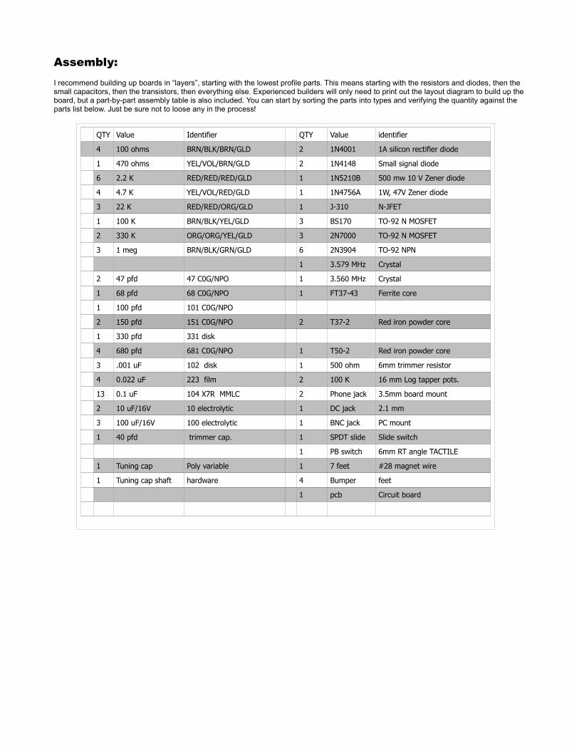
Assembly:I recommend building up boards in “layers”, starting with the lowest profile parts. This means starting with the resistors and diodes, then the small capacitors, then the transistors, then everything else. Experienced builders will only need to print out the layout diagram to build up the board, but a part-by-part assembly table is also included. You can start by sorting the parts into types and verifying the quantity against the parts list below. Just be sure not to loose any in the process!
QTY Value Identifier QTY Value identifier
4 100 ohms BRN/BLK/BRN/GLD 2 1N4001 1A silicon rectifier diode
1 470 ohms YEL/VOL/BRN/GLD 2 1N4148 Small signal diode
6 2.2 K RED/RED/RED/GLD 1 1N5210B 500 mw 10 V Zener diode
4 4.7 K YEL/VOL/RED/GLD 1 1N4756A 1W, 47V Zener diode
3 22 K RED/RED/ORG/GLD 1 J-310 N-JFET
1 100 K BRN/BLK/YEL/GLD 3 BS170 TO-92 N MOSFET
2 330 K ORG/ORG/YEL/GLD 3 2N7000 TO-92 N MOSFET
3 1 meg BRN/BLK/GRN/GLD 6 2N3904 TO-92 NPN
1 3.579 MHz Crystal
2 47 pfd 47 C0G/NPO 1 3.560 MHz Crystal
1 68 pfd 68 C0G/NPO 1 FT37-43 Ferrite core
1 100 pfd 101 C0G/NPO
2 150 pfd 151 C0G/NPO 2 T37-2 Red iron powder core
1 330 pfd 331 disk
4 680 pfd 681 C0G/NPO 1 T50-2 Red iron powder core
3 .001 uF 102 disk 1 500 ohm 6mm trimmer resistor
4 0.022 uF 223 film 2 100 K 16 mm Log tapper pots.
13 0.1 uF 104 X7R MMLC 2 Phone jack 3.5mm board mount
2 10 uF/16V 10 electrolytic 1 DC jack 2.1 mm
3 100 uF/16V 100 electrolytic 1 BNC jack PC mount
1 40 pfd trimmer cap. 1 SPDT slide Slide switch
1 PB switch 6mm RT angle TACTILE
1 Tuning cap Poly variable 1 7 feet #28 magnet wire
1 Tuning cap shaft hardware 4 Bumper feet
1 pcb Circuit board

Layout Diagram: color
Print out this layout diagram for reference while building.

Resistors and diodes:
Parts are numbered on the board from upper left corner, left to right and zig-zag towards the bottom (front edge) of the board.
Look out for resistors with similar color codes which only vary by the 3d zero multiplier band, such as 2.2K vs 22K, 470 ohm vs 4.7K or 47 K and the like.
Be careful not to mix up D5 (a zener) with D1 and D2 (small signal silicon) diodes, since they are both in similar glass packages.
R1 100 K BRN/BLK/YEL/GLD R2 470 OHM YEL/VOL/BRN/GLD
R3 4.7 K YEL/VOL/RED/GLD R4 1 M BRN/BLK/GRN/GLD
R5 2.2 K RED/RED/RED/GLD R6 2.2 K RED/RED/RED/GLD
R7 330 K ORG/ORG/YEL/GLD R8 100 OHM BRN/BLK/BRN/GLD
R9 4.7 K YEL/VOL/RED/GLD R10 2.2 K RED/RED/RED/GLD
R11 4.7 K YEL/VOL/RED/GLD R12 100 OHM BRN/BLK/BRN/GLD
R13 1 M BRN/BLK/GRN/GLD R14 2.2 K RED/RED/RED/GLD
R15 Not used, leave blank R16 DELETED Location
R17 330 K ORG/ORG/YEL/GLD R18 2.2 K RED/RED/RED/GLD
R19 100 OHM BRN/BLK/BRN/GLD R20 22 K RED/RED/ORG/GLD
R21 22 K RED/RED/ORG/GLD R22 4.7 K YEL/VOL/RED/GLD
R23 2.2 K RED/RED/RED/GLD R24 22 K RED/RED/ORG/GLD
R25 1 M BRN/BLK/GRN/GLD R26 100 OHM BRN/BLK/BRN/GLD
D1 1N4148 Small glass D2 1N4148 Small, glass
D3 1N4756A Large, glass D4 1N4001 Large, black plastic 1A, 50V
D5 1N5240B Small, glass – don't mix up with 4148 diodes!
D6 1N4001 Large, black plastic

Capacitors:
All the 0.1 uF (104) caps are highlighted in yellow, since these are the most numerous value. The 0.022 uF caps are highlighted in green, as these are film caps. All other values are in light blue. Install the electrolytic caps last. Be sure to observe polarity. The plus end is the long lead. The negative lead pad is circled on the silk screen and highlighted in black below for the 100 uF caps.
C1 681 680 pfd, C0G C2a,b 681 680 pfd, C0G
C3 681 680 pfd, C0G C4 104 0.1 ufd X7R
C5 151 150 pfd, C0G/NPO C6 101 100 pfd C0G/NPO
C7 104 0.1 ufd X7R C8 104 0.1 ufd X7R
C9 104 0.1 ufd X7R C10 104 0.1 ufd X7R
C11 104 0.1 ufd X7R C12 100 100 ufd 16V electrolytic
C13 104 0.1 ufd X7R C14 100 100 ufd 16V electrolytic
C15 104 0.1 ufd X7R C16 151 150 pfd C0G/NPO
C17 223 0.022 ufd film C18 104 0.1 ufd X7R
C19 10 10 ufd / 16V electrolytic C20 10 10 ufd / 16V electrolytic
C21 331 330 pfd disk C22 102 0.001 ufd disk
C23 102 0.001 ufd disk C24 102 0.001 ufd disk
C25 223 0.022 ufd film C26 104 0.1 ufd X7R
C27 104 0.1 ufd X7R C28 47 47 pfd C0G/NPO
C29 223 0.022 ufd film C30 68 68 pfd C0G/NPO
C31 223 0.022 ufd film C32 104 0.1 ufd X7R
C33 47 47 pfd C0G/NPO C34 100 100 ufd 16V electrolytic

Remaining parts:
Note: due to the close spacing of the variable resistors and tuning cap, you might want to mount the pots to the bottom of the board, although that will make the controls work “backwards” and require a taller box to give clearance to the knobs. Or they could be mounted off the board and the connections jumpered to the board.
Q1 2N7000
Q2 BS170
Q3 BS170
Q4 BS170
Q5 2N3904
Q6 2N7000
Q7 2N3904
Q8 2N7000
Q9 2N3904
Q10 2N3904
Q11 J310
Q12 2N3904
Q13 2N3904
J3/4 PHONE JACK
J2 DC POWER
J1 BNC JACK
S1 SPDT SLIDE SWITCH
S2 PUSH BUTTON RIGHT ANGLE TACKLE SWITH
X1 3.579 MHz CRYSTAL or 3 pin SIP socket
X2 3.560 MHz CRYSTAL or 3 pin SIP socket
V1 501 500 OHM TRIMMER RESISTOR
V2/3 100 K 16mm Log potentiometer
C36 VARIABLE Tuning cap
C35 Trimmer cap

[Type text]
Addendum There are two style poly-varicon capacitors that may come with your kit. Both styles are detailed below and latest variety needs a slight modification. Poly-varicon installation to kits ordered before 01/20/18 [ ] Prior to installing the poly-varicon variable capacitors the leads must be re-routed through the snap-on cover. The pictures below show the “as received” and “modified” condition. Carefully pry off the cover, bend the leads to the rear, feed them through the cover and snap it back on. There is a small tab, opposite the side with the leads, on the cover that matches the body of the poly-varicon for the cover to fit properly.
As received Modified [ ] Adjust the two trimmer caps on the back of each poly-varicon to their minimum value as shown
below.
[ ] Install the two polyvaricon capacitors on the inside of the front panel. Carefully feed the three leads through the board and secure the capacitors with the two short metric Phillips screws from the outside. Solder and clip the leads flush. Install the nylon spacers, long metric screws, and knobs as shown in the figure below.

[Type text]
Poly-varicon installation to kits ordered after 01/20/18
As received Modified The polyvaricons as received, need a modification to allow the leads to reach the bottom of the device so it can be soldered to the pcb. If bent without modifying the cover, all the leads will not reach. Shown above is the un-modified polyvaricon as received. Carefully unsnap the protective cover. Deepen all three slots for the connection tabs by ~1/8” with an Exacto knife as shown on the right. Snap the cover back on, and run the leads on the outside of the cover.
Shown below the modified cover is snapped back on and the leads are bent to the bottom. It is now ready for installation. As you can see, one of the leads is shorter than the others and may need to be soldered on the top of the board. This is not a problem with plated through holes.

[Type text]
[ ] Adjust the two trimmer caps on the back of each poly-varicon to their minimum value as shown
below.

Toroids:
The toroid cores should be wound with the wire fairly tight and flush to the body of the core. Loops which extend much beyond the outside edge of the core need to be avoided. The recommended wire lengths in the table include a 1” start and stop wire length. If you run out of wire, your winding the core too loosely. A loosely wound core will not have the required inductance and will affect the tuning window, stability and power output. Note: When installing L3, you'll need to give it a “half twist” after soldering the leads to make it fit between Q4 and the cap on the other side, so leave a little slack in the leads.
Winding the receiver input transformer, T1:
The receiver input has three windings, the input coupling, the receiver tuned circuit inductor and the feedback winding. The tuned circuit inductor winding and the feedback winding require to have a specific phase relationship for the detector to oscillate and produce audio output. Winding the core as explained below will ensure the proper phase relationship when mounted to the board. A piece of double sided foam tape or a nylon screw and fiber washer can be used to secure the T1 core to the board to reduce microphonics and improve stability.
● Cut a length of #28 magnet wire to 40”● Wind the initial 38 turns for the detector input.● Make a hairpin about 1” long and continue to wind an additional 5 turns.● Break out another 1” hairpin and wind 5 more turns. ● All these turns will just fit around the core with little space to spare. ● Now snip the center of the hairpin turn to separate the three windings. ● Tin the leads and install into the board, making sure you don't cross winding leads. ● Once the toroids are installed, assembly is complete. ● Be sure to carefully inspect your solder joints before power up the board.
Test and operation:
A common 13.8V supply is recommended. So is adding a 1A fuse. Since the board it's self isn't fused, using a fused supply cable will prevent any possible damage to the supply or board if something went wrong with the assembly or soldering and a short develops.
Warning: The common on the headphone jack is “hot” and connected to the input supply directly through the headphones. Therefore, a short here to ground could burn out the headphones.
● Plug in a set of headphones● Connect BNC jack to 80 meter antenna● Plug in a DC power cable● Using a small blade screwdriver, adjust the REGEN control pot fully counter clock wise. ● Turn on the power supply● Check for +10 V at the pad labeled “TP3” If this is not 10V, then you have a 1N4148 diode there instead of the zener. ● Check for about 1.8 V at TP1 and 13.0 V at TP2 (this assumes a 13.8V power supply)● Turn the REGEN control slowly clockwise. You should start to hear band noise at about ¼ turn. This is when the detector starts to
oscillate. Advance the control a little more to ensure reliable start up. If your using a frequency counter adjust for a stable reading on the display.
● You should now be able to tune around and hear stations. ● The C35 trimmer cap can be used to set the lower frequency tuning point you would like.
Transmitter testing:
● Connect a QRP power meter and 50 ohm dummy load to BNC jack● Plug in a straight key into key jack.● Power up board with 13.8 volts● Key the transmitter.● Power output should be about 2.5 to 3 watts. The power will sag a little if keyed for more then a few seconds.● Side tone should be audible in the headphones.
L1 T37-2 (red)
17” #28 magnet wire, 28 turns
L2 T37-2 (red)
17” #28 magnet wire, 29 turns
L3 FT-37-43 (black)
6” #28 magnet wire, 8 turns
Snip loops af ter w inding.

SPOT switch:
The spot switch allows finding your transmit frequency in the receiver. Simply push the switch and tune the receiver until you hear the tone you like and side band with the least QRM.
Adding a frequency readout dial.
A frequency counter can be added for a direct readout of the receiver frequency. The pads labeled “S” (signal) and “G” (ground) in the box labeled “FREQ” on the right side of the board connect to the counters signal input. The Pads labeled “+” (plus power) and “-” (ground) in the box labeled “FREQ COUNT” supply power to the counter board. This supply is isolated from the rest of the circuits on the board via a 100 ohm resistor and 100 ufd electrolytic capacitor. This keeps power supply noise from the counter out of the receiver.
Note that the counter can also radiate a fair amount of noise which can be picked up by the transmitter low pass filter coils and the receiver input coil. Therefore, try to mount the counter as far away from the coils as possible or add some shielding behind the counter board.
A suitable counter is available from the QRP Guys, QRPKITS.com or from China sourced from ebay.
Adding a speaker:
The headphone jack has switched contacts, so it would be possible to wire up a small 32 ohm speaker. There should be sufficient volume for most signals. Make sure it's a 32 ohm type, an 8 ohm will be too much of a load. Connect the speaker leads to the two pads to the left of the headphone jack.
Supply voltage:
The Para80set is designed to be powered by 13.8 volts. It will work reliably down to 12 volts with reduced power output. Power output can be improved by removing a turn from L1, making it 27 turns instead of 28.
Excessive SWR:
Due to the narrow bandwidth of most 80 meter antennas, high SWR can be a problem. Excessive SWR could lead to stability problems or even damage to the PA. It is recommended to use a resistive SWR bridge when using an antenna tuner to find best match.
Trouble shooting:
Any trouble getting the rig to work will inevitably be tracked down to an assembly error, the most common of which are soldering issues. A close visual inspection of your soldering will likely find the problem area. Having miss placed parts is less likely, but a possibility, especially the mixing up of resistors with similar color codes. Voltages at critical points are noted on the schematic. Using your voltmeter to verify these voltages can help pin point the problem area. Minor variations from the voltages noted on the schematic are normal due to parts tolerances, voltmeter loading and calibration.
Packaging the board:
The simplest way to make an enclosure for the board would be a “L” shape, made of PCB material or aluminum. Just remember that the exposed mounting sleeve of the headphone jack is “live” with the DC supply so make sure it has good clearance from a conductive front panel. A front panel drill drawing is shown below. To fully enclose the board, a cover could be made of some thin hobby wood which would make for a nice looking package. The diagram below should print out to actual size so it can be used as a drill template, but be sure to double check the dimensions first to make sure. The hight of the panel below the board will depend on what you use for board spacers. I would use at least an inch.

Schematic:
PCB track layout:
© KD1JV Designs and QRPGUYS.com 2017