the open electrical & electronic engineering journal the open electrical & electronic...
TRANSCRIPT
Send Orders for Reprints to [email protected]
The Open Electrical & Electronic Engineering Journal, 2017, 11, 125-140 125
1874-1290/17 2017 Bentham Open
The Open Electrical & ElectronicEngineering Journal
Content list available at: www.benthamopen.com/TOEEJ/
DOI: 10.2174/1874129001711010125
REVIEW ARTICLE
Optimization and Design of Integrated Space Target
Mingxi Xue*
Collaborative Innovation Center for Micro Nano Fabrication, Device and System State Key Laboratory of PrecisionMeasurement Technology and Instruments Department of Precision Instrument Tsinghua University, Beijing, 100084,P.R. China
Received: May 04, 2016 Revised: September 09, 2016 Accepted: October 10, 2016
Abstract:
Background & Objective:
The design and optimization of laser detection system based on MEMS (Micro-electro Mechanical Systems) scanning mirror ispresented in the paper. According to requirements of application, it adopts the laser module to design the laser driver circuit, and thedesigned modulation circuit can satisfy the actual needs.
Method:
The designed information processing module is composed of the echo receiving module, signal amplification and filter circuitmodule, and the synchronous circuit of measuring angle and distance, etc.
Conclusion:
It gives out the distance decoding method and explores the method of capturing echo signal, which can fast and accurately calculatethe distance and azimuth information of scanning.
Keywords: MEMS, Micro Scanning Mirror, Integration, Space target, Detection, Design.
1. INTRODUCTION
In the scanning methods of the optical system, the traditional mechanical scanning system is the most widelyadopted method, which includes mirror, prism scanning, etc. It has the advantages of simple structure and largescanning angle, etc. but its limitation is that it has large inertia of mechanical movement, low scanning speed, heavyweight, etc. The acoustic optic/electro-optic or binary optical scanning are emerging technologies in recent years, andtheir scanning speeds are very fast, but the scanning angles are relatively small and the power consumption is also large,and the most important aspect is that their efficiencies are low, and their driving structures are complicated andexpensive. Therefore, in order to realize miniaturization, low power consumption, low cost and large scanning angle,and high stability two-dimensional MEMS scanning mirror equipment by using the MEMS technology, the basic andmost important step is to develop the space laser scanning detection system.
In 1980, Kurt e. Petersen published the first article about MEMS scanning mirror [1], known as the research work ofMEMS scanning device which has been lasted for more than 30 years. The research of early MEMS scanning devicefocuses on the imaging, such as the confocal microscopy [2 - 7], the bar code recognition [8], the fingerprint recognition[9], etc. Other applications include the optical coherence tomography technique (OCT) [10], the retinal scan display (RSD) [11], printer, head-up display and the laser radar (LIDAR) in the automated production lines [12, 13].
* Address correspondence to this author at the Collaborative Innovation Center for Micro Nano Fabrication, Device and System State Key Laboratoryof Precision Measurement Technology and Instruments Department of Precision Instrument Tsinghua University, Beijing, 100084, P. R. China,E-mail: [email protected]

126 The Open Electrical & Electronic Engineering Journal, 2017, Volume 11 Mingxi Xue
The Germany Fraunhofer institute studied the damping model, vacuum sealing [14, 15], closed-loop control [16],angular sensor of electrostatic comb drive in their research work. In 2009, the IPMS group of Germany's Fraunhoferinstitute studied the integration piezoresistive angular sensor on two-dimensional micro MEMS scanning mirror, whosesensitivity can reach 0.42 mV/V°. Fraunhofer institute of Germany adopts the method of scattering force point,optimizing structure of supporting to improve the dynamic deformation of micro mirror. After improvement, thedesigned micro mirror dynamic flatness is five times higher than the design of the IPMS team. The resonance frequencyof the micro mirror is 16 KHz. The diameter of mirror is 1 mm, the mechanical deflection angle is about 10°, which cansatisfy the imaging demand of VGA (640×480 pixels), and the dynamic deformation is relative small. It is based on thedesign and optimization of laser detection system of MEMS scanning mirror, according to the need of goal application,it adopts the laser module to complete the design of laser driver circuit, and modulation circuit.
The designed system information processing module mainly includes echo receiving circuit design, signalamplification and filter circuit design, angle and distance synchronous circuit design, etc.
The design of detection system of non-cooperative target is shown in Fig. (1), which is mainly composed of laser,modulation unit, MEMS two-dimensional micro scanning mirror, piezoresistive measuring unit, the light receiving unitand a signal processing unit, et al. The principle target detection and measurement of system is that the modulation unitproduces modulation signal to start the laser and the beam of laser scanning and detecting the measured target, throughthe reflex lenses of the micro two-dimensional scanning mirror, scanning beam can make detection to target objects, itwill produce the reflected beams, which can be received by the photoelectric detector in the receiving unit, and itreceives signal and echo signal and outputs them to the signal processing unit.
According to the measurement signal of deflection angle of the two-dimensional MEMS micro scanning mirror, thesignal processing unit can calculate the relative orientation of target and according to the phase difference of the echosignal and modulation signal; it calculates the relative distance of the target and the specific location information of thetarget can be obtained.
The work of whole system involves the measuring of distance and angle. The main working principle of distancepart is that the modulation circuit generates the driving laser source of the modulation signal. Loading a carrier on theemission laser, the beam emitted by the laser source will be launched to space through the scanning micro mirror. In theprocess of laser scanning in the space, if the scanning light meets the objects such as space debris, satellite, etc., it willbe scattered. The scattering light beam of the receiving target of the echo receiving circuit can produce echo signal, andthrough the processing, the echo signal will present pulse signal form. In the comparison of the pulse echo signal andlocal signal used by the laser modulation, it adopts phase comparison ranging method to calculate the target relativedistance. The main working principle of angular part is that the piezoresistive angle measuring circuit of scanning micromirror produces the deflection angle signal, and triggers the angle information which can be collected by the echoreceiving circuit, and it gets the time point of two-dimensional scanning deflection angle corresponding to the reflectedbeams.
Fig. (1). Diagram of the laser scanning measuring system.
Scan beam
Laser beamLaser Receiving unit
Object
Signal processionunit
Reflected beam
Measurementsignal
Receivingsignal
Two-dimensionalMicro-mirror
Azimuth of objectModulationUnit
ModulationSignal
Echo signal
Ddistance of object
ModulationSignal
Detection System Based on MEMS Micro-scanning Mirror The Open Electrical & Electronic Engineering Journal, 2017, Volume 11 127
Through the target's relative distance information, two-dimensional deflection angle information, it can commonlyget the space relative position information of target related system. On the basis of the principle prototype, theintegration design and packaging of the scan detection system can be made. Detection system test is based on MEMSmicro mirror, it can build test platform to complete the system test and field test accurately. The system environmentaladaptability and typical environmental measurements are also researched.
2. MAIN DESIGN OF SYSTEM
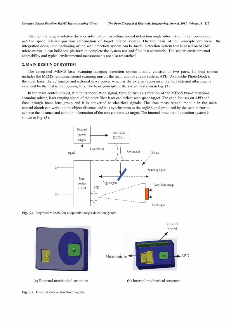
The integrated MEMS laser scanning imaging detection system mainly consists of two parts. Its host systemincludes the MEMS two-dimensional scanning mirror, the main control circuit system, APD (Avalanche Photo Diode),the fiber laser, the collimator and external drive power which is the external accessory, the half external attachmentsextended by the host is the focusing lens. The basic principle of the system is shown in Fig. (2).
In the main control circuit, it outputs modulation signal, through two axis rotation of the MEMS two-dimensionalscanning mirror, laser ranging signal of the outer fiber laser can reflect scan space target. The echo focuses on APD endface through focus lens group and it is converted to electrical signals. The time measurement module in the maincontrol circuit can work out the object distance, and it is synchronous to the angle signal produced by the scan mirror toachieve the distance and azimuth information of the non-cooperative target. The internal structure of detection system isshown in Fig. (3).
Fig. (2). Integrated MEMS non-cooperative target detection system.
Fig. (3). Detection system structure diagram.
Fiber laser(external)
Externalpowersupply
Maincontrolcircuit
SignalLaser driver Collimator
Angle signal
The host
Scanning signal
APD
Echo signal
Focus lens group
Circuitboard
Micro-mirror APD
(a) External mechanical structure (b) Internal mechanical structure
128 The Open Electrical & Electronic Engineering Journal, 2017, Volume 11 Mingxi Xue
3. DESIGN OF DETECTION SYSTEM
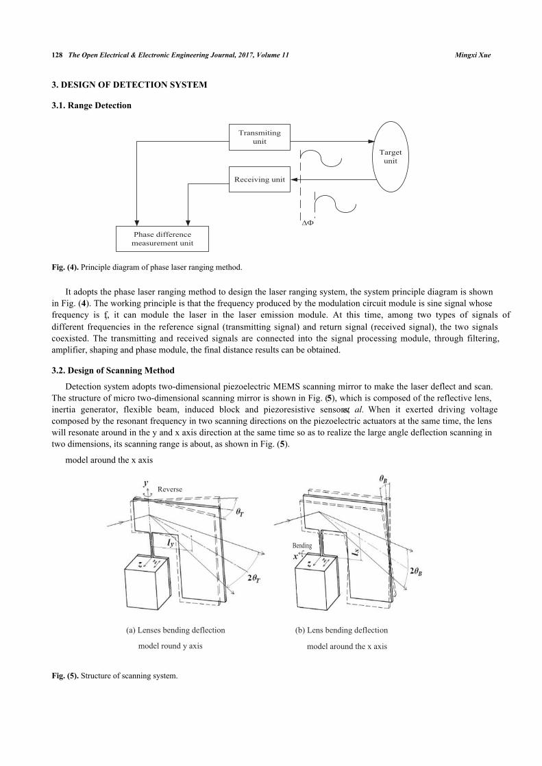
3.1. Range Detection
Fig. (4). Principle diagram of phase laser ranging method.
It adopts the phase laser ranging method to design the laser ranging system, the system principle diagram is shownin Fig. (4). The working principle is that the frequency produced by the modulation circuit module is sine signal whosefrequency is fs, it can module the laser in the laser emission module. At this time, among two types of signals ofdifferent frequencies in the reference signal (transmitting signal) and return signal (received signal), the two signalscoexisted. The transmitting and received signals are connected into the signal processing module, through filtering,amplifier, shaping and phase module, the final distance results can be obtained.
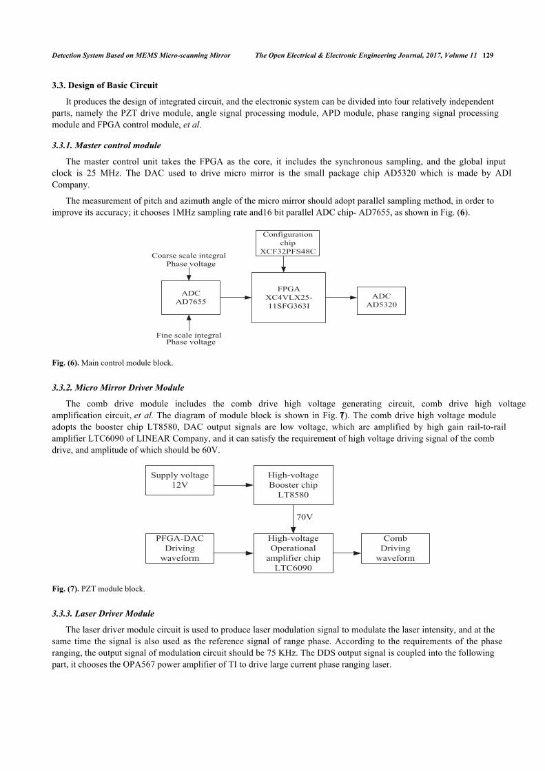
3.2. Design of Scanning Method
Detection system adopts two-dimensional piezoelectric MEMS scanning mirror to make the laser deflect and scan.The structure of micro two-dimensional scanning mirror is shown in Fig. (5), which is composed of the reflective lens,inertia generator, flexible beam, induced block and piezoresistive sensors, et al. When it exerted driving voltagecomposed by the resonant frequency in two scanning directions on the piezoelectric actuators at the same time, the lenswill resonate around in the y and x axis direction at the same time so as to realize the large angle deflection scanning intwo dimensions, its scanning range is about, as shown in Fig. (5).
model around the x axis
Fig. (5). Structure of scanning system.
Phase differencemeasurement unit
Transmitingunit
Receiving unit
Targetunit
��
Reverse
Bending
(a) Lenses bending deflection
model round y axis
(b) Lens bending deflection
model around the x axis
Detection System Based on MEMS Micro-scanning Mirror The Open Electrical & Electronic Engineering Journal, 2017, Volume 11 129
3.3. Design of Basic Circuit
It produces the design of integrated circuit, and the electronic system can be divided into four relatively independentparts, namely the PZT drive module, angle signal processing module, APD module, phase ranging signal processingmodule and FPGA control module, et al.
3.3.1. Master control module
The master control unit takes the FPGA as the core, it includes the synchronous sampling, and the global inputclock is 25 MHz. The DAC used to drive micro mirror is the small package chip AD5320 which is made by ADICompany.
The measurement of pitch and azimuth angle of the micro mirror should adopt parallel sampling method, in order toimprove its accuracy; it chooses 1MHz sampling rate and16 bit parallel ADC chip- AD7655, as shown in Fig. (6).
Fig. (6). Main control module block.
3.3.2. Micro Mirror Driver Module
The comb drive module includes the comb drive high voltage generating circuit, comb drive high voltageamplification circuit, et al. The diagram of module block is shown in Fig. (7). The comb drive high voltage moduleadopts the booster chip LT8580, DAC output signals are low voltage, which are amplified by high gain rail-to-railamplifier LTC6090 of LINEAR Company, and it can satisfy the requirement of high voltage driving signal of the combdrive, and amplitude of which should be 60V.
Fig. (7). PZT module block.
3.3.3. Laser Driver Module
The laser driver module circuit is used to produce laser modulation signal to modulate the laser intensity, and at thesame time the signal is also used as the reference signal of range phase. According to the requirements of the phaseranging, the output signal of modulation circuit should be 75 KHz. The DDS output signal is coupled into the followingpart, it chooses the OPA567 power amplifier of TI to drive large current phase ranging laser.
ADCAD7655
FPGAXC4VLX25-11SFG363I
ADCAD5320
Configurationchip
XCF32PFS48CCoarse scale integral
Fine scale integral
Phase voltage
Phase voltage
Supply voltage12V
High-voltageBooster chip
LT8580
High-voltageOperational
amplifier chipLTC6090
PFGA-DACDriving
waveform
CombDriving
waveform
70V

130 The Open Electrical & Electronic Engineering Journal, 2017, Volume 11 Mingxi Xue
3.3.4. APD and Signal Module
The APD and signal module mainly include the adjustable APD voltage automatic gain control module, APD signalautomatic gain control module and APD. In order to generate adjustable APD output function, it increases a three-timediode double voltage circuits based on the high pressure output of MAX1932ETC, and in order to curb the influence oftemperature change on the output voltage, it adopts the thermal RT1 as temperature compensation device.
The automatic gain control circuit adopts TI-THS7530 automatic gain amplifier, the variable gain amplifier ofwhich is from 11.6 dB to 46.5 dB, whose gain slope is 38.8 dB/V and the bandwidth is 300 MHz, which is the totaldifferential input and output and it is quite suitable for the APD detector with a pre-amplifier, differential output(Fig. 8).
Fig. (8). APD module.
3.3.5. Phase Ranging Signal Processing Module
The phase ranging signal processing module mainly involves the filter circuit and phase pulse generating circuit. Itdesigns a band-pass filter whose center frequency is 75 KHz; it extracts the sine signal to prepare for the subsequentphase. In the phase detecting circuit, the output of band-pass filter whose center frequency is 75 KHz is put into high-speed comparator ADCMP600, and then the sine wave signal converted the square wave signal, and then it is imputedinto the FPGA to make the phase to be verified and then the measurement results with large scale are obtained (Fig. 9).
3.3.6. Angle Signal Processing Module
Fig. (9). Angle signal processing module block.
The angle signal processing module adopts the PCap01 capacitance digital conversion chips of ACAMCompany, when measurement frequency is 10 KHz, which has 12 capacitance measurement precision,whose highest measurement frequency can be up to 500 KHz. The angle changes of X axis and Y axis willcause the changes of capacitance sensors, through PCap01 Digital Conversion Chip (CDC) it can measurethe capacitance value of the sensor and it also can measure the angle, the angle information of two axis iscommunicated with main control chip through the SPI bus.
Adjustable highvoltage chip
MAX1932ETC
Diode voltagedoubling circuit
DFLS1100
APDSCD-SAR
00H2
Automaticgain chip
Rangeprocessing
module
Lasercircuit
Differentialsignal
Y axis Anglemeasuringcapacitance
X axis Anglemeasuringcapacitance
DigitalconversionCapacitance
PCap01
Main controlchipTwo axis
angle
Detection System Based on MEMS Micro-scanning Mirror The Open Electrical & Electronic Engineering Journal, 2017, Volume 11 131
3.3.7. Integrated Design of System
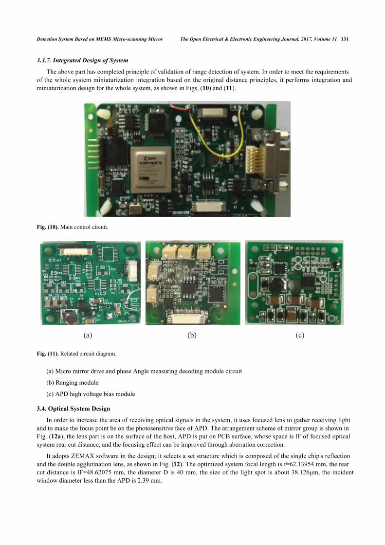
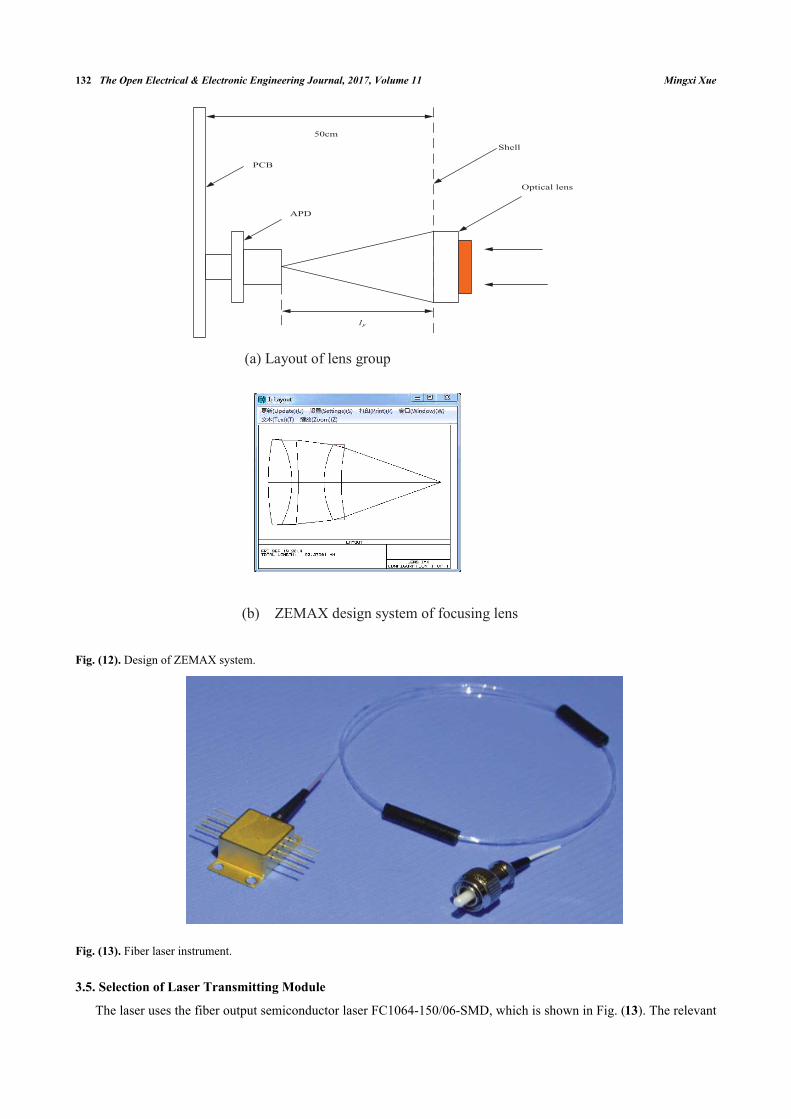
The above part has completed principle of validation of range detection of system. In order to meet the requirementsof the whole system miniaturization integration based on the original distance principles, it performs integration andminiaturization design for the whole system, as shown in Figs. (10) and (11).
Fig. (10). Main control circuit.
Fig. (11). Related circuit diagram.
(a) Micro mirror drive and phase Angle measuring decoding module circuit
(b) Ranging module
(c) APD high voltage bias module
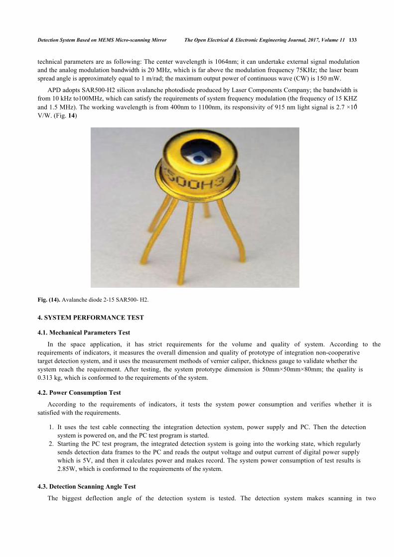
3.4. Optical System Design
In order to increase the area of receiving optical signals in the system, it uses focused lens to gather receiving lightand to make the focus point be on the photosensitive face of APD. The arrangement scheme of mirror group is shown inFig. (12a), the lens part is on the surface of the host, APD is put on PCB surface, whose space is lF of focused opticalsystem rear cut distance, and the focusing effect can be improved through aberration correction.
It adopts ZEMAX software in the design; it selects a set structure which is composed of the single chip's reflectionand the double agglutination lens, as shown in Fig. (12). The optimized system focal length is f=62.13954 mm, the rearcut distance is lF=48.62075 mm, the diameter D is 40 mm, the size of the light spot is about 38.126μm, the incidentwindow diameter less than the APD is 2.39 mm.
(a) (b) (c)
132 The Open Electrical & Electronic Engineering Journal, 2017, Volume 11 Mingxi Xue
Fig. (12). Design of ZEMAX system.
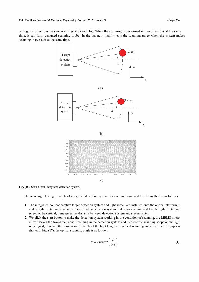
Fig. (13). Fiber laser instrument.
3.5. Selection of Laser Transmitting Module
The laser uses the fiber output semiconductor laser FC1064-150/06-SMD, which is shown in Fig. (13). The relevant
50cm
PCB
APD
Optical lens
Shell
Fl
(a) Layout of lens group
(b) ZEMAX design system of focusing lens
Detection System Based on MEMS Micro-scanning Mirror The Open Electrical & Electronic Engineering Journal, 2017, Volume 11 133
technical parameters are as following: The center wavelength is 1064nm; it can undertake external signal modulationand the analog modulation bandwidth is 20 MHz, which is far above the modulation frequency 75KHz; the laser beamspread angle is approximately equal to 1 m/rad; the maximum output power of continuous wave (CW) is 150 mW.
APD adopts SAR500-H2 silicon avalanche photodiode produced by Laser Components Company; the bandwidth isfrom 10 kHz to100MHz, which can satisfy the requirements of system frequency modulation (the frequency of 15 KHZand 1.5 MHz). The working wavelength is from 400nm to 1100nm, its responsivity of 915 nm light signal is 2.7 ×10⁶
V/W. (Fig. 14)
Fig. (14). Avalanche diode 2-15 SAR500- H2.
4. SYSTEM PERFORMANCE TEST
4.1. Mechanical Parameters Test
In the space application, it has strict requirements for the volume and quality of system. According to therequirements of indicators, it measures the overall dimension and quality of prototype of integration non-cooperativetarget detection system, and it uses the measurement methods of vernier caliper, thickness gauge to validate whether thesystem reach the requirement. After testing, the system prototype dimension is 50mm×50mm×80mm; the quality is0.313 kg, which is conformed to the requirements of the system.
4.2. Power Consumption Test
According to the requirements of indicators, it tests the system power consumption and verifies whether it issatisfied with the requirements.
It uses the test cable connecting the integration detection system, power supply and PC. Then the detection1.system is powered on, and the PC test program is started.Starting the PC test program, the integrated detection system is going into the working state, which regularly2.sends detection data frames to the PC and reads the output voltage and output current of digital power supplywhich is 5V, and then it calculates power and makes record. The system power consumption of test results is2.85W, which is conformed to the requirements of the system.
4.3. Detection Scanning Angle Test
The biggest deflection angle of the detection system is tested. The detection system makes scanning in two
134 The Open Electrical & Electronic Engineering Journal, 2017, Volume 11 Mingxi Xue
orthogonal directions, as shown in Figs. (15) and (16). When the scanning is performed in two directions at the sametime, it can form designed scanning probe. In the paper, it mainly tests the scanning range when the system makesscanning in two axis at the same time.
Fig. (15). Scan sketch Integrated detection system.
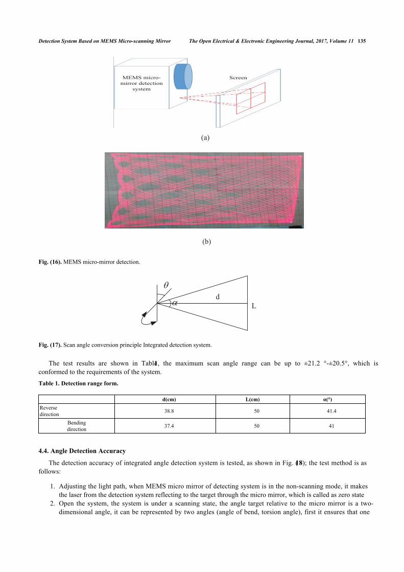
The scan angle testing principle of integrated detection system is shown in figure, and the test method is as follows:
The integrated non-cooperative target detection system and light screen are installed onto the optical platform, it1.makes light center and screen overlapped when detection system makes no scanning and lets the light center andscreen to be vertical, it measures the distance between detection system and screen center.We click the start button to make the detection system working in the condition of scanning, the MEMS micro-2.mirror makes the two-dimensional scanning in the detection system and measure the scanning scope on the lightscreen grid, in which the conversion principle of the light length and optical scanning angle on quadrille paper isshown in Fig. (17), the optical scanning angle is as follows:
(1)
Targetdetectionsystem
z
x�
Target
(a)
Targetdetectionsystem
z
y
Target
�
(b)
-1 -0.8 -0.6 -0.4 -0.2 0 0.2 0.4 0.6 0.8 1-1
-0.8
-0.6
-0.4
-0.2
0
0.2
0.4
0.6
0.8
1
(c)
2arctan2Ld
� � � � �
Detection System Based on MEMS Micro-scanning Mirror The Open Electrical & Electronic Engineering Journal, 2017, Volume 11 135
Fig. (16). MEMS micro-mirror detection.
Fig. (17). Scan angle conversion principle Integrated detection system.
The test results are shown in Table 1, the maximum scan angle range can be up to ±21.2 °-±20.5°, which isconformed to the requirements of the system.
Table 1. Detection range form.
d(cm) L(cm) α(°)Reversedirection 38.8 50 41.4
Bendingdirection 37.4 50 41
4.4. Angle Detection Accuracy
The detection accuracy of integrated angle detection system is tested, as shown in Fig. (18); the test method is asfollows:
Adjusting the light path, when MEMS micro mirror of detecting system is in the non-scanning mode, it makes1.the laser from the detection system reflecting to the target through the micro mirror, which is called as zero stateOpen the system, the system is under a scanning state, the angle target relative to the micro mirror is a two-2.dimensional angle, it can be represented by two angles (angle of bend, torsion angle), first it ensures that one
MEMS micro-mirror detection
system
Screen
(a)
(b)
dL
�
�

136 The Open Electrical & Electronic Engineering Journal, 2017, Volume 11 Mingxi Xue
angle target relative to the micro mirror is constant, turning the turntable, and then another angle target relativeto the micro mirror will be changed.
The rotating platform rotate respectively to 2.5°; 5°;7.5°; 10 °; 12.5 °; 15° in both sides and it collects a total of 12collection data points, and they can be directly read from screen of PC, and at the same time it can record and read thedeviation angle.
Changing the micro mirror coordinate system, it repeats step 2, it makes measurement of the target position of1.another direction angle.According to the formula (2), it can respectively calculate the arithmetic mean value of two directions angular2.error.
(2)
Fig. (18). Angle measuring accuracy test of integrated detection system.
The test results of angle measuring accuracy are shown in Table 2, and two axis angle measuring accuracy isrespectively ±0.185 ° and ± 0.171 °,which are better than the index requirements.
Table 2. Angle measuring accuracy test record.
Test Reversing angle(°) Test value(°) Deviation(°) Reversing angle
(°)Test value
(°) Deviation(°)
Reversing
0.000 0.187 0.187 0.000 -0.117 -0.1172.500 2.695 0.195 -2.500 -2.719 -0.2195.000 4.898 -0.102 -5.000 -5.616 -0.1167.500 7.609 0.109 -7.500 -7.223 0.27710.000 10.124 0.124 -10.000 -10.162 -0.16212.500 12.375 -0.125 -12.500 -12.639 -0.13915.000 15.175 0.175 -15.000 -14.837 0.163
1 2 ... n
n� � �� � �� � ��
�
PC Received data
Target
Rotary table
(a) Schematic diagram (b) physical diagram
Detection System Based on MEMS Micro-scanning Mirror The Open Electrical & Electronic Engineering Journal, 2017, Volume 11 137
Test Reversing angle(°) Test value(°) Deviation(°) Reversing angle
(°)Test value
(°) Deviation(°)
Bending
0.000 0.109 0.109 -0.000 -0.103 -0.1032.500 2.337 -0.163 -2.500 -2.628 -0.1285.000 5.182 0.182 -5.000 -5.157 -0.1577.500 7.356 -0.144 -7.500 -7.623 -0.12310.000 10.158 0.158 -10.000 -10.176 -0.17612.500 12.129 -0.371 -12.500 +12.625 -0.12515.000 15.167 0.167 -15.000 -15.135 -0.135
4.5. Test of Range Detection Accuracy
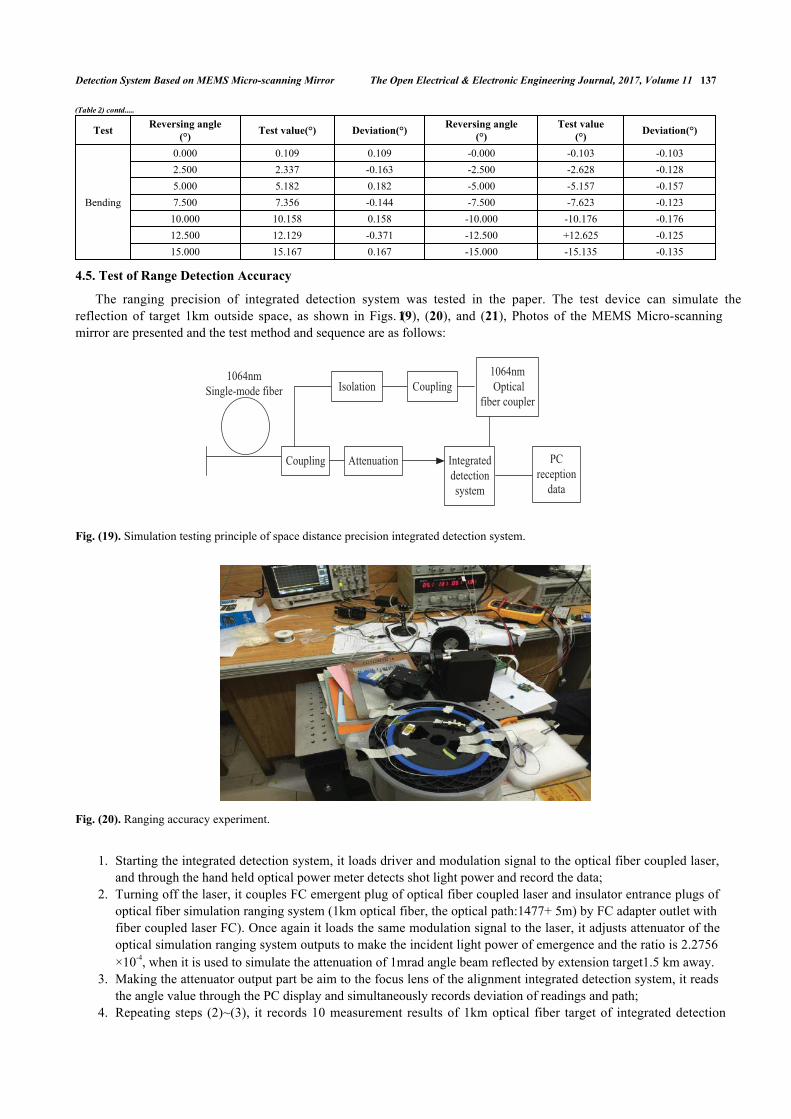
The ranging precision of integrated detection system was tested in the paper. The test device can simulate thereflection of target 1km outside space, as shown in Figs. (19), (20), and (21), Photos of the MEMS Micro-scanningmirror are presented and the test method and sequence are as follows:
Fig. (19). Simulation testing principle of space distance precision integrated detection system.
Fig. (20). Ranging accuracy experiment.
Starting the integrated detection system, it loads driver and modulation signal to the optical fiber coupled laser,1.and through the hand held optical power meter detects shot light power and record the data;Turning off the laser, it couples FC emergent plug of optical fiber coupled laser and insulator entrance plugs of2.optical fiber simulation ranging system (1km optical fiber, the optical path:1477+ 5m) by FC adapter outlet withfiber coupled laser FC). Once again it loads the same modulation signal to the laser, it adjusts attenuator of theoptical simulation ranging system outputs to make the incident light power of emergence and the ratio is 2.2756×10⁻⁴, when it is used to simulate the attenuation of 1mrad angle beam reflected by extension target1.5 km away.Making the attenuator output part be aim to the focus lens of the alignment integrated detection system, it reads3.the angle value through the PC display and simultaneously records deviation of readings and path;Repeating steps (2)~(3), it records 10 measurement results of 1km optical fiber target of integrated detection4.
(Table 2) contd.....
Coupling Attenuation
Isolation Coupling1064nmOptical
fiber coupler
Integrateddetectionsystem
PCreception
data
1064nmSingle-mode fiber
138 The Open Electrical & Electronic Engineering Journal, 2017, Volume 11 Mingxi Xue
system, according to the type (3), the average value can be calculated, and reference accuracy index can beobtained accordingly;
(3)
5 The optical fiber analog ranging system is replace with 500m (optical fiber: 739±5m), repeat steps (1)~(4).
The test results are shown in Table 3, when optical path is 1477±5m, the ranging error is about ±3.1m, when opticalpath is 739m±5m, the ranging error is about ±2.4 m, which is far better than the requirements.
Fig. (21). Photo of the MEMS Micro-scanning Mirror.
5. KEY TECHNOLOGY AND RELATED INDICATORS
In the laser detection system based on MEMS scanning mirror design, the focus is the breakthrough of high SNRweak echo signal detection of integrated circuit design, high scan speed quick and high precision angle measuringdistance measurement method research and its circuit implementation, and engineering prototype can be completed.
Model of the system is analyzed, and the after multistage enlarging echo signal is passed through FPGA for signalprocessing, finally, it can realize the weak echo signal detection, and the system miniaturization can be achieved; itadopts FPGA as the master control chip, using the parallel I/O mouth for data reading and writing, the angle anddistance of parallel processing can be realized, target orientation detection can also be made.
Table 3. The ranging accuracy test record.
Tests No Test value(m) Deviation(m) Tests Test value(m) Deviation(m)
1km single mode fiber(Opticalpath:1477±5m)
Ttransmit:98.25mWReceive:22.35μW
1 1468.8 -8.2
500m single mode fiber(Opticalpath:739±5m)
Transmit:102.38mWReceive:93.19μW
746.2 7.22 1468.9 -8.1 744.1 5.13 1489.8 12.8 740.1 1.14 1490.2 13.2 742.3 3.35 1481.1 4.1 730.1 -8.96 1493.5 16.5 750.4 11.47 1481.2 4.2 736.5 -2.58 1475.6 -1.4 746.8 7.89 1470.5 -6.5 743.4 4.410 1474.5 -2.5 741.2 2.2
Mean value — 1479.4 — — 742.1 —
In the integrated MEMS non-cooperative target detection system, its quality is less than 500 g, volume is less than50 ×50×80 mm3, and power consumption is not higher than 3W. Scan range is more than 40°×40°, the azimuthmeasurement precision is better than 0.2°, ranging accuracy is about 50 m; Temperature range is from -20ºC to 40ºC,20Krad (Si) can meet the requirement of anti-radiation ability, the mechanical conditions are shown in Tables 4 and 5.
1 2 ... nL L LLn
� � �

Detection System Based on MEMS Micro-scanning Mirror The Open Electrical & Electronic Engineering Journal, 2017, Volume 11 139
Table 4. Conditions of sine vibration test.
Frequency(Hz) Requirements(o-p) 10~20 7.45mm 20~100 12g
Scan frequency 4oct/min Loading direction Three axial direction
Table 5. Conditions of random vibration test.
Frequency (Hz) Density of power spectral 10~100 3dB/oct 100~600 0.075g2/Hz 600~2000 -6dB/oct
Total mean square value 8.53gms Loading time 1min
Loading direction Three axial direction
CONCLUSION
According to actual needs of space target angle measurement, it puts forward a decoupling bi-axial angle1.measuring sensor MEMS scanning mirror, on the basis of the principle prototype and scanning coverageanalysis, it optimizes the device structure and the resonance frequency, engineering prototype design iscompleted.It adopts MEMS two-dimensional scanning mirror and active laser ranging technology, the integrated non-2.cooperative target detection system which has a small volume, light quality, low power, and scanning speed andso on, which is suitable for small space target detection, and it provides powerful means for the application ofspace satellite.Individual technical indicators of the system are still need to further optimized, take the volume for example,3.index factor should be 50×50 ×80 mm3, if detection range is greater than 40°×40°, then the numerical apertureof system is at least more than 0.34. In the receiving system the aperture of system should be 40 mm, when focallength is 60 mm, numerical aperture should be 0.31, the received aperture angle is 36.8°, as it is strictly unableto meet the requirements of maximum detection range. Short edge of the system is only 50 mm in size, however,if it takes the size of optical margin pressure and mechanical installation into consideration, it will make thesystem unable to match the larger aperture receiving system.
Although it can shorten the focal length, etc. in order to meet the requirements of numerical aperture,thickness of the center of the lens itself should also be increased, however, it will increase the extension ofthe original attachment size, in return, it can affect the scan window 40 visual scopes.
In the design, the detecting light source is taken as the external component, which is independent of the system,1.and in order to make the system integration degree be low, it still needs a higher degree of integration.
CONFLICT OF INTEREST
The author confirms that this article content has no conflict of interest.
ACKNOWLEDGEMENTS
Declared none.
REFERENCES
[1] C-C. Yang, K. Chao, and Y-R. Chen, "Development of multispectral image processing algorithms for identification of wholesome septicemic,and inflammatory process chickens", J. Food Eng., vol. 69, pp. 225-234, 2005.[http://dx.doi.org/10.1016/j.jfoodeng.2004.07.021]

140 The Open Electrical & Electronic Engineering Journal, 2017, Volume 11 Mingxi Xue
[2] G. Petrie, "Airborne Digital Frame Cameras", GEO Informat., vol. 10, pp. 18-27, 2003.
[3] Y. Lei, Z. Shi-hu, and L. Zhou-hui, "A Convertible Aerial Camera System Integrated With Film and CCD Image Sensor", In: InternationalSymposium on Photoelectronic Detection and Imaging, 2007, p. 662414.
[4] S. Morrison, "A New Type of photosensitive Junction Device", Solid-State Electron., vol. 5, pp. 485-494, 1963.[http://dx.doi.org/10.1016/0038-1101(63)90033-9]
[5] W.S. Boyle, and G.E. Smith, "Charge coupled semiconductor devices", Bell Syst. Tech. J., vol. 49, pp. 587-583, 1970.[http://dx.doi.org/10.1002/j.1538-7305.1970.tb01790.x]
[6] J. Horton, R. Mazza, and H. Dym, "The scanner- A solid-state image scanner", Proc. IEEE, vol. 5, pp. 1513-1528, 1964.[http://dx.doi.org/10.1109/PROC.1964.3440]
[7] M.A. Schuster, and G. Strull, "A monolithic mosaic of photon sensors for solid state imaging application", IEEE Trans. Electron. Dev., vol.13, pp. 907-912, 1966.[http://dx.doi.org/10.1109/T-ED.1966.15867]
[8] H.A. Yang, T.L. Tang, and S.T. Lee, "A novel coilless scanning mirror using eddy current lorentz force and magnetostatic force", J.Microelectromech. Syst., vol. 16, no. 3, pp. 511-520, 2007.[http://dx.doi.org/10.1109/JMEMS.2007.896708]
[9] H. Miyajima, N. Asaoka, and T. Isokawa, "A MEMS electromagnetic optical scanner for a commercial confocal laser scanning microscope",J. Microelectromech. Syst., vol. 12, no. 3, pp. 243-251, 2003.[http://dx.doi.org/10.1109/JMEMS.2003.809961]
[10] S.H. Ahn, and Y.K. Kim, "Silicon scanning mirror of two DOF with compensation current routing", J. Micromech. Microeng., vol. 14, no. 11,pp. 1455-1461, 2004.[http://dx.doi.org/10.1088/0960-1317/14/11/004]
[11] A. Jain, and H. Xie, "A single-crystal silicon micromirror for large bi-directional 2D scanning applications", Sens. Actuators A Phys., vol.130, pp. 454-460, 2006.[http://dx.doi.org/10.1016/j.sna.2005.10.030]
[12] J. Singh, T. Gan, and A. Agarwal, "3D free space thermally actuated micromirror device", Sens. Actuators A Phys., vol. 123, pp. 468-475,2005.[http://dx.doi.org/10.1016/j.sna.2005.02.037]
[13] X.H. Xu, and Y. Feng, "Design, fabrication and characterization of a bulk-PZT-actuated MEMS deformable mirror", J. Micromech.Microeng., vol. 17, no. 12, pp. 2439-2446, 2007.[http://dx.doi.org/10.1088/0960-1317/17/12/008]
[14] N. Kikuchi, Y. Haga, and M. Maeda, "Piezolectric 2D micro scanner for minimally invasive therapy fabricated using femtosecond laserablation", In: IEEE International Solid-State Sensors and Actuators Conference, 2003, pp. 603-606.[http://dx.doi.org/10.1109/SENSOR.2003.1215545]
[15] S.J. Kim, Y.H. Cho, and H.J. Nam, "Piezoelectrically pushed rotational micromirrors for wide-angle optical switch applications", In: 16thIEEE Annual International Conference on Micro Electro Mechanical Systems, 2003, pp. 263-266.[http://dx.doi.org/10.1109/MEMSYS.2003.1189736]
[16] L.X. Zhou, M. Last, and V. Milanovic, "Two-axis scanning mirror for free-space optical communication between UAVs", In: IEEE/LEOSInternational Conference on Optical MEMS, 2003, pp. 157-158.[http://dx.doi.org/10.1109/OMEMS.2003.1233514]
© 2017 Mingxi Xue.
This is an open access article distributed under the terms of the Creative Commons Attribution 4.0 International Public License (CC-BY 4.0), acopy of which is available at: https://creativecommons.org/licenses/by/4.0/legalcode. This license permits unrestricted use, distribution, andreproduction in any medium, provided the original author and source are credited.