the nintendo gameboy
TRANSCRIPT
The Nintendo Gameboy.
The GameBoy is a toy. Or is it?
I will be clear from day one: the GameBoy is a toy. And apretty good one too. I never played with one until a few weeks ago, when I was at a family gathering. The kids left it for what it was. The moment I picked the damned thing up, I recognized that this machine has a lot more to offer than entertainment for adolescent fingers. So I started to dig something deeper into the world of the GameBoy...
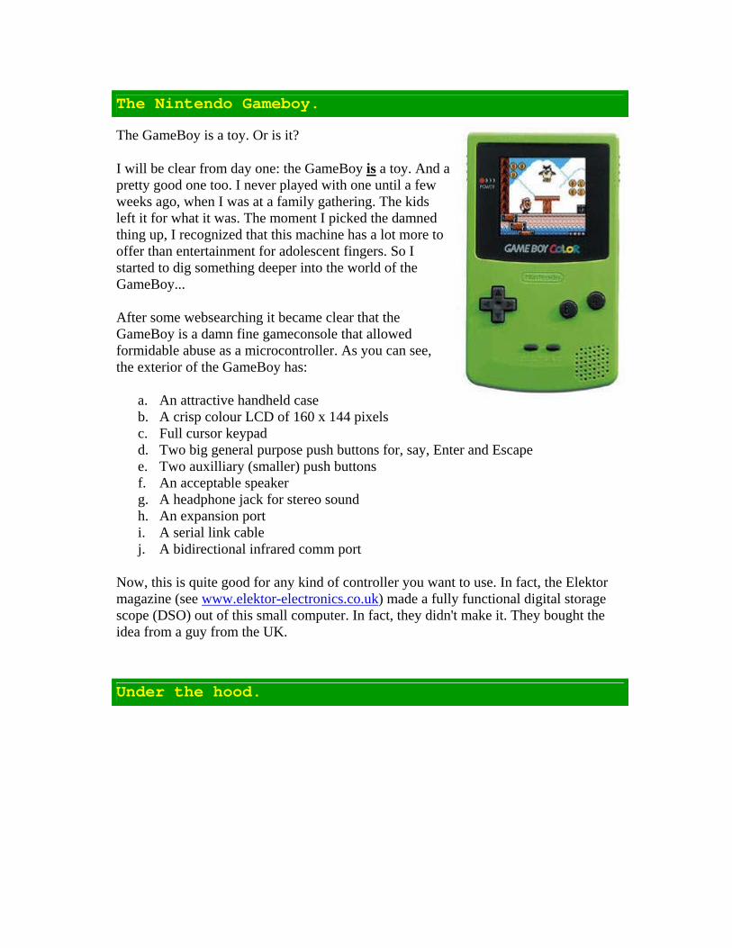
After some websearching it became clear that the GameBoy is a damn fine gameconsole that allowed formidable abuse as a microcontroller. As you can see, the exterior of the GameBoy has:
a. An attractive handheld case b. A crisp colour LCD of 160 x 144 pixels c. Full cursor keypad d. Two big general purpose push buttons for, say, Enter and Escape e. Two auxilliary (smaller) push buttons f. An acceptable speaker g. A headphone jack for stereo sound h. An expansion port i. A serial link cable j. A bidirectional infrared comm port
Now, this is quite good for any kind of controller you want to use. In fact, the Elektor magazine (see www.elektor-electronics.co.uk) made a fully functional digital storage scope (DSO) out of this small computer. In fact, they didn't make it. They bought the idea from a guy from the UK.
Under the hood.
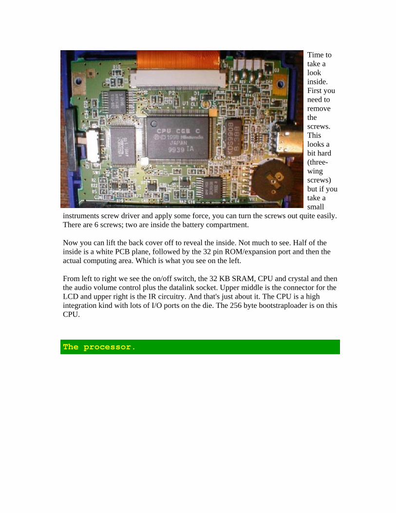
Time to take a look inside. First you need to remove the screws. This looks a bit hard (three-wing screws) but if ytake a small
instruments screw driver and apply some force, you can turn the screws out quite easily. There are 6 screws; two are inside the battery compartment.
ou
Now you can lift the back cover off to reveal the inside. Not much to see. Half of the inside is a white PCB plane, followed by the 32 pin ROM/expansion port and then the actual computing area. Which is what you see on the left.
From left to right we see the on/off switch, the 32 KB SRAM, CPU and crystal and then the audio volume control plus the datalink socket. Upper middle is the connector for the LCD and upper right is the IR circuitry. And that's just about it. The CPU is a high integration kind with lots of I/O ports on the die. The 256 byte bootstraploader is on this CPU.
The processor.

The CPU is a stripped down version of the Zilog Z80A. It lacks a lot of instructions and some registers but it packs a lot of punch in a big (128 pin)
package.
For microcontroller applications this reduction is no big deal. We don't need 23 registers. The usual 7 will do perfectly well. On the left we see the main trio again. The LH52256 is the 32 KB SRAM that is mapped to part of the upper 32 KB of the address space via bankswitching. Above it is the LCD controller and to the right we see our beloved Z80 clone.
I took the liberty to borrow some figures from related websites:
o Circuit layout of Gameboy (monochrome) o Schematic overview o Link-cable and expansion port layout
Game cartridges.
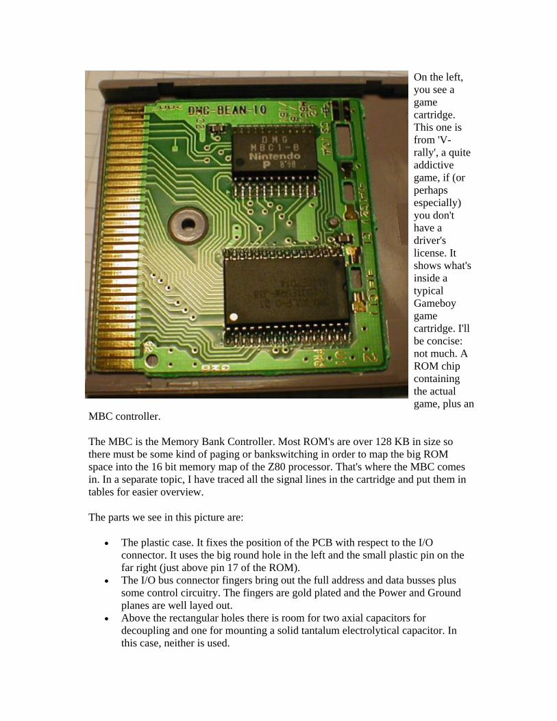
On the left, you see a game cartridge. This one is from 'V-rally', a quite addictive game, if (or perhaps especially) you don't have a driver's license. It shows what's inside a typical Gameboy game cartridge. I'll be concise: not much. A ROM chip containing the actual game, plus a
MBC controller. n
The MBC is the Memory Bank Controller. Most ROM's are over 128 KB in size so there must be some kind of paging or bankswitching in order to map the big ROM space into the 16 bit memory map of the Z80 processor. That's where the MBC comes in. In a separate topic, I have traced all the signal lines in the cartridge and put them in tables for easier overview.
The parts we see in this picture are:
• The plastic case. It fixes the position of the PCB with respect to the I/O connector. It uses the big round hole in the left and the small plastic pin on the far right (just above pin 17 of the ROM).
• The I/O bus connector fingers bring out the full address and data busses plus some control circuitry. The fingers are gold plated and the Power and Ground planes are well layed out.
• Above the rectangular holes there is room for two axial capacitors for decoupling and one for mounting a solid tantalum electrolytical capacitor. In this case, neither is used.
• The Memory Bank Controller is in the top right section. MBC1 is a 24 pin surface mount circuit. It maps the 128 KB ROM in 16 KB windows into the Z80 memory map.
• The ROM is in the lower right. It's a 32 pin device. It gets the lower 15 address lines from the CPU and the rest comes from the MBC.
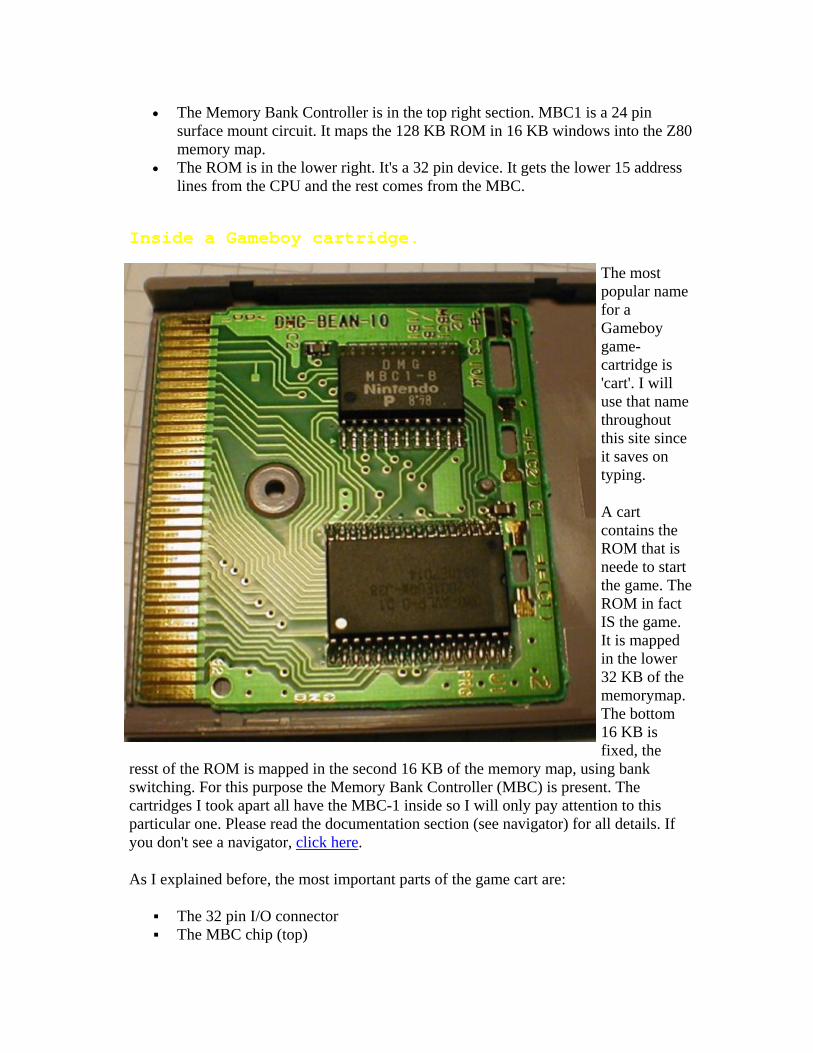
Inside a Gameboy cartridge.
The most popular name for a Gameboy game-cartridge is 'cart'. I will use that name throughout this site since it saves on typing.
A cart contains the ROM that is neede to start the game. TROM in fact IS the gameIt is mappedin the lower 32 KB of the memoryThe bottom 16 KB is fixed, the
resst of the ROM is mapped in the second 16 KB of the memory map, using bank switching. For this purpose the Memory Bank Controller (MBC) is present. The cartridges I took apart all have the MBC-1 inside so I will only pay attention to this particular one. Please read the documentation section (see navigator) for all details. If you don't see a navigator,
he
.
map.
click here.
As I explained before, the most important parts of the game cart are:
The 32 pin I/O connector The MBC chip (top)
The ROM chip (bottom)
For this particular cart, I removed the ROM and traced all signal lines, which I will tell about in the remainder of this page.
This cart is meant to become a kind of docking station for hardware extensions. I'm not sure how I will do it. There are roughly two methods right now:
a. Connect a flatcable between the ROM connections to a ZIF socket for an external ROM and run all the I/O signals to a 34 pin header for external circuitry
b. Only lead the I/O connector pins out
The first option is best since I will be able to use the original MBC for bankswitching. On the other hand, a home made application that is not a game will rarely need more than 16 KB of object code, so the necessity of bankswitching will be very low. Time will tell what is the best method.
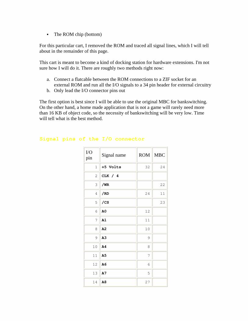
Signal pins of the I/O connector
I/O pin Signal name ROM MBC
1 +5 Volts 32 24
2 CLK / 4
3 /WR 22
4 /RD 24 11
5 /CS 23
6 A0 12
7 A1 11
8 A2 10
9 A3 9
10 A4 8
11 A5 7
12 A6 6
13 A7 5
14 A8 27
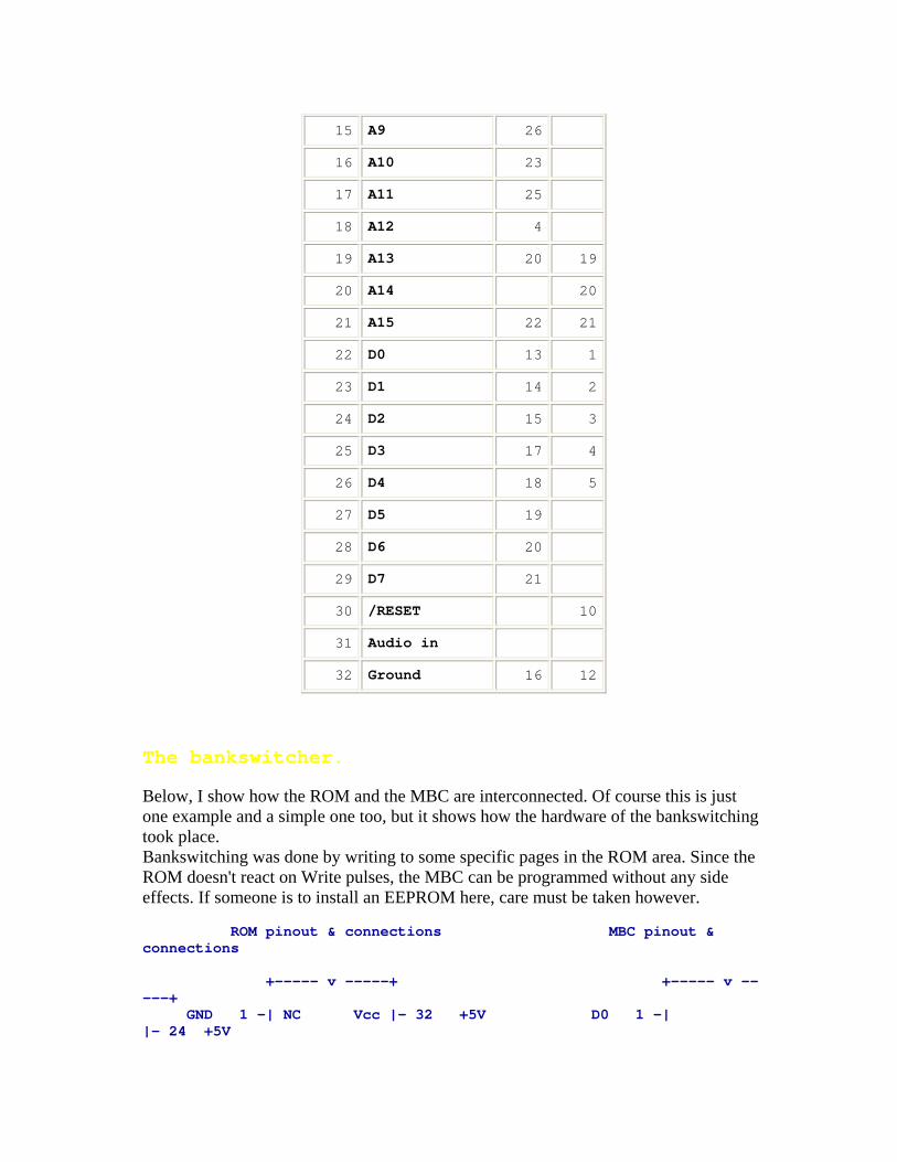
15 A9 26
16 A10 23
17 A11 25
18 A12 4
19 A13 20 19
20 A14 20
21 A15 22 21
22 D0 13 1
23 D1 14 2
24 D2 15 3
25 D3 17 4
26 D4 18 5
27 D5 19
28 D6 20
29 D7 21
30 /RESET 10
31 Audio in
32 Ground 16 12
The bankswitcher.
Below, I show how the ROM and the MBC are interconnected. Of course this is just one example and a simple one too, but it shows how the hardware of the bankswitching took place. Bankswitching was done by writing to some specific pages in the ROM area. Since the ROM doesn't react on Write pulses, the MBC can be programmed without any side effects. If someone is to install an EEPROM here, care must be taken however. ROM pinout & connections MBC pinout & connections +----- v -----+ +----- v -----+ GND 1 -| NC Vcc |- 32 +5V D0 1 -| |- 24 +5V
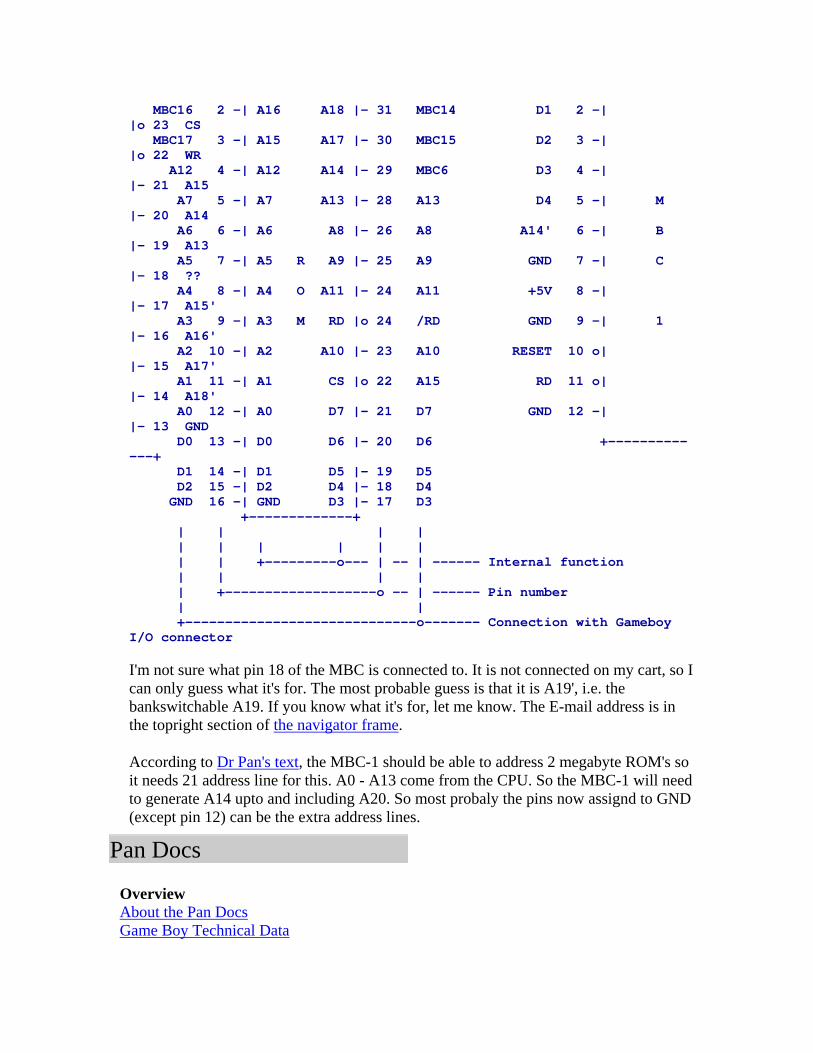
MBC16 2 -| A16 A18 |- 31 MBC14 D1 2 -| |o 23 CS MBC17 3 -| A15 A17 |- 30 MBC15 D2 3 -| |o 22 WR A12 4 -| A12 A14 |- 29 MBC6 D3 4 -| |- 21 A15 A7 5 -| A7 A13 |- 28 A13 D4 5 -| M |- 20 A14 A6 6 -| A6 A8 |- 26 A8 A14' 6 -| B |- 19 A13 A5 7 -| A5 R A9 |- 25 A9 GND 7 -| C |- 18 ?? A4 8 -| A4 O A11 |- 24 A11 +5V 8 -| |- 17 A15' A3 9 -| A3 M RD |o 24 /RD GND 9 -| 1 |- 16 A16' A2 10 -| A2 A10 |- 23 A10 RESET 10 o| |- 15 A17' A1 11 -| A1 CS |o 22 A15 RD 11 o| |- 14 A18' A0 12 -| A0 D7 |- 21 D7 GND 12 -| |- 13 GND D0 13 -| D0 D6 |- 20 D6 +-------------+ D1 14 -| D1 D5 |- 19 D5 D2 15 -| D2 D4 |- 18 D4 GND 16 -| GND D3 |- 17 D3 +-------------+ | | | | | | | | | | | | +---------o--- | -- | ------ Internal function | | | | | +-------------------o -- | ------ Pin number | | +-----------------------------o------- Connection with Gameboy I/O connector I'm not sure what pin 18 of the MBC is connected to. It is not connected on my cart, so I can only guess what it's for. The most probable guess is that it is A19', i.e. the bankswitchable A19. If you know what it's for, let me know. The E-mail address is in the topright section of the navigator frame.
According to Dr Pan's text, the MBC-1 should be able to address 2 megabyte ROM's so it needs 21 address line for this. A0 - A13 come from the CPU. So the MBC-1 will need to generate A14 upto and including A20. So most probaly the pins now assignd to GND (except pin 12) can be the extra address lines.
Pan Docs Overview About the Pan Docs Game Boy Technical Data
Memory Map I/O Ports Video Display Sound Controller Joypad Input Serial Data Transfer (Link Cable) Timer and Divider Registers Interrupts CGB Registers SGB Functions CPU Specifications CPU Registers and Flags CPU Instruction Set CPU Comparision with Z80 Cartridges The Cartridge Header Memory Bank Controllers Gamegenie/Shark Cheats Other Power Up Sequence Reducing Power Consumption Sprite RAM Bug External Connectors
About the Pan Docs ================================================================= Everything You Always Wanted To Know About GAMEBOY * =================================================================
* but were afraid to ask
Pan of -ATX- Document Updated by contributions from: Marat Fayzullin, Pascal Felber, Paul Robson, Martin Korth CPU, SGB, CGB, AUX specs by Martin Korth
Last updated 10/2001 by nocash Previously updated 4-Mar-98 by kOOPa
Forward The following was typed up for informational purposes regarding the inner workings on
the hand-held game machine known as GameBoy, manufactured and designed by Nintendo Co., LTD. This info is presented to inform a user on how their Game Boy works and what makes it "tick". GameBoy is copyrighted by Nintendo Co., LTD. Any reference to copyrighted material is not presented for monetary gain, but for educational purposes and higher learning. Available Document Formats The present version of this document is available in Text and Html format: http://www.work.de/nocash/pandocs.txt http://www.work.de/nocash/pandocs.htm
Also, a copy of this document is included in the manual of newer versions of the no$gmb debugger, because of recent piracy attacks (many thanks and best wishes go to hell) I have currently no intention to publish any such or further no$gmb updates though.
Game Boy Technical Data CPU - 8-bit (Similar to the Z80 processor) Clock Speed - 4.194304MHz (4.295454MHz for SGB, max. 8.4MHz for CGB) Work RAM - 8K Byte (32K Byte for CGB) Video RAM - 8K Byte (16K Byte for CGB) Screen Size - 2.6" Resolution - 160x144 (20x18 tiles) Max sprites - Max 40 per screen, 10 per line Sprite sizes - 8x8 or 8x16 Palettes - 1x4 BG, 2x3 OBJ (for CGB: 8x4 BG, 8x3 OBJ) Colors - 4 grayshades (32768 colors for CGB) Horiz Sync - 9198 KHz (9420 KHz for SGB) Vert Sync - 59.73 Hz (61.17 Hz for SGB) Sound - 4 channels with stereo sound Power - DC6V 0.7W (DC3V 0.7W for GB Pocket, DC3V 0.6W for CGB)
Memory Map The gameboy is having a 16bit address bus, that is used to address ROM, RAM, and I/O registers. General Memory Map 0000-3FFF 16KB ROM Bank 00 (in cartridge, fixed at bank 00) 4000-7FFF 16KB ROM Bank 01..NN (in cartridge, switchable bank number) 8000-9FFF 8KB Video RAM (VRAM) (switchable bank 0-1 in CGB Mode) A000-BFFF 8KB External RAM (in cartridge, switchable bank, if any) C000-CFFF 4KB Work RAM Bank 0 (WRAM) D000-DFFF 4KB Work RAM Bank 1 (WRAM) (switchable bank 1-7 in CGB Mode) E000-FDFF Same as C000-DDFF (ECHO) (typically not used)
FE00-FE9F Sprite Attribute Table (OAM) FEA0-FEFF Not Usable FF00-FF7F I/O Ports FF80-FFFE High RAM (HRAM) FFFF Interrupt Enable Register
Jump Vectors in First ROM Bank The following addresses are supposed to be used as jump vectors: 0000,0008,0010,0018,0020,0028,0030,0038 for RST commands 0040,0048,0050,0058,0060 for Interrupts
However, the memory may be used for any other purpose in case that your program doesn't use any (or only some) RST commands or Interrupts. RST commands are 1-byte opcodes that work similiar to CALL opcodes, except that the destination address is fixed. Cartridge Header in First ROM Bank The memory at 0100-014F contains the cartridge header. This area contains information about the program, its entry point, checksums, information about the used MBC chip, the ROM and RAM sizes, etc. Most of the bytes in this area are required to be specified correctly. For more information read the chapter about The Cartridge Header. External Memory and Hardware The areas from 0000-7FFF and A000-BFFF may be used to connect external hardware. The first area is typically used to address ROM (read only, of course), cartridges with Memory Bank Controllers (MBCs) are additionally using this area to output data (write only) to the MBC chip. The second area is often used to address external RAM, or to address other external hardware (Real Time Clock, etc). External memory is often battery buffered, and may hold saved game positions and high scrore tables (etc.) even when the gameboy is turned of, or when the cartridge is removed. For specific information read the chapter about Memory Bank Controllers.
Video Display Video I/O Registers LCD Control Register LCD Status Register LCD Interrupts LCD Position and Scrolling LCD Monochrome Palettes LCD Color Palettes (CGB only) LCD VRAM Bank (CGB only) LCD OAM DMA Transfers LCD VRAM DMA Transfers (CGB only) Video Memory VRAM Tile Data
VRAM Background Maps VRAM Sprite Attribute Table (OAM) Accessing VRAM and OAM
LCD Control Register FF40 - LCDC - LCD Control (R/W) Bit 7 - LCD Display Enable (0=Off, 1=On) Bit 6 - Window Tile Map Display Select (0=9800-9BFF, 1=9C00-9FFF) Bit 5 - Window Display Enable (0=Off, 1=On) Bit 4 - BG & Window Tile Data Select (0=8800-97FF, 1=8000-8FFF) Bit 3 - BG Tile Map Display Select (0=9800-9BFF, 1=9C00-9FFF) Bit 2 - OBJ (Sprite) Size (0=8x8, 1=8x16) Bit 1 - OBJ (Sprite) Display Enable (0=Off, 1=On) Bit 0 - BG Display (for CGB see below) (0=Off, 1=On)
LCDC.7 - LCD Display Enable CAUTION: Stopping LCD operation (Bit 7 from 1 to 0) may be performed during V-Blank ONLY, disabeling the display outside of the V-Blank period may damage the hardware. This appears to be a serious issue, Nintendo is reported to reject any games that do not follow this rule. V-blank can be confirmed when the value of LY is greater than or equal to 144. When the display is disabled the screen is blank (white), and VRAM and OAM can be accessed freely. --- LCDC.0 has different Meanings depending on Gameboy Type --- LCDC.0 - 1) Monochrome Gameboy and SGB: BG Display When Bit 0 is cleared, the background becomes blank (white). Window and Sprites may still be displayed (if enabled in Bit 1 and/or Bit 5). LCDC.0 - 2) CGB in CGB Mode: BG and Window Master Priority When Bit 0 is cleared, the background and window lose their priority - the sprites will be always displayed on top of background and window, independently of the priority flags in OAM and BG Map attributes. LCDC.0 - 3) CGB in Non CGB Mode: BG and Window Display When Bit 0 is cleared, both background and window become blank (white), ie. the Window Display Bit (Bit 5) is ignored in that case. Only Sprites may still be displayed (if enabled in Bit 1). This is a possible compatibility problem - any monochrome games (if any) that disable the background, but still want to display the window wouldn't work properly on CGBs.
LCD Status Register
FF41 - STAT - LCDC Status (R/W) Bit 6 - LYC=LY Coincidence Interrupt (1=Enable) (Read/Write) Bit 5 - Mode 2 OAM Interrupt (1=Enable) (Read/Write) Bit 4 - Mode 1 V-Blank Interrupt (1=Enable) (Read/Write) Bit 3 - Mode 0 H-Blank Interrupt (1=Enable) (Read/Write) Bit 2 - Coincidence Flag (0:LYC<>LY, 1:LYC=LY) (Read Only) Bit 1-0 - Mode Flag (Mode 0-3, see below) (Read Only) 0: During H-Blank 1: During V-Blank 2: During Searching OAM-RAM 3: During Transfering Data to LCD Driver
The two lower STAT bits show the current status of the LCD controller. Mode 0: The LCD controller is in the H-Blank period and the CPU can access both the display RAM (8000h-9FFFh) and OAM (FE00h-FE9Fh)
Mode 1: The LCD contoller is in the V-Blank period (or the display is disabled) and the CPU can access both the display RAM (8000h-9FFFh) and OAM (FE00h-FE9Fh)
Mode 2: The LCD controller is reading from OAM memory. The CPU <cannot> access OAM memory (FE00h-FE9Fh) during this period.
Mode 3: The LCD controller is reading from both OAM and VRAM, The CPU <cannot> access OAM and VRAM during this period. CGB Mode: Cannot access Palette Data (FF69,FF6B) either.
The following are typical when the display is enabled: Mode 2 2_____2_____2_____2_____2_____2___________________2____ Mode 3 _33____33____33____33____33____33__________________3___ Mode 0 ___000___000___000___000___000___000________________000 Mode 1 ____________________________________11111111111111_____
The Mode Flag goes through the values 0, 2, and 3 at a cycle of about 109uS. 0 is present about 48.6uS, 2 about 19uS, and 3 about 41uS. This is interrupted every 16.6ms by the VBlank (1). The mode flag stays set at 1 for about 1.08 ms. Mode 0 is present between 201-207 clks, 2 about 77-83 clks, and 3 about 169-175 clks. A complete cycle through these states takes 456 clks. VBlank lasts 4560 clks. A complete screen refresh occurs every 70224 clks.)
LCD Interrupts INT 40 - V-Blank Interrupt

The V-Blank interrupt occurs ca. 59.7 times a second on a regular GB and ca. 61.1 times a second on a Super GB (SGB). This interrupt occurs at the beginning of the V-Blank period (LY=144). During this period video hardware is not using video ram so it may be freely accessed. This period lasts approximately 1.1 milliseconds. INT 48 - LCDC Status Interrupt There are various reasons for this interrupt to occur as described by the STAT register ($FF40). One very popular reason is to indicate to the user when the video hardware is about to redraw a given LCD line. This can be useful for dynamically controlling the SCX/SCY registers ($FF43/$FF42) to perform special video effects.
LCD Position and Scrolling FF42 - SCY - Scroll Y (R/W) FF43 - SCX - Scroll X (R/W) Specifies the position in the 256x256 pixels BG map (32x32 tiles) which is to be displayed at the upper/left LCD display position. Values in range from 0-255 may be used for X/Y each, the video controller automatically wraps back to the upper (left) position in BG map when drawing exceeds the lower (right) border of the BG map area. FF44 - LY - LCDC Y-Coordinate (R) The LY indicates the vertical line to which the present data is transferred to the LCD Driver. The LY can take on any value between 0 through 153. The values between 144 and 153 indicate the V-Blank period. Writing will reset the counter. FF45 - LYC - LY Compare (R/W) The gameboy permanently compares the value of the LYC and LY registers. When both values are identical, the coincident bit in the STAT register becomes set, and (if enabled) a STAT interrupt is requested. FF4A - WY - Window Y Position (R/W) FF4B - WX - Window X Position minus 7 (R/W) Specifies the upper/left positions of the Window area. (The window is an alternate background area which can be displayed above of the normal background. OBJs (sprites) may be still displayed above or behinf the window, just as for normal BG.) The window becomes visible (if enabled) when positions are set in range WX=0..166, WY=0..143. A postion of WX=7, WY=0 locates the window at upper left, it is then completly covering normal background.
LCD Monochrome Palettes
FF47 - BGP - BG Palette Data (R/W) - Non CGB Mode Only This register assigns gray shades to the color numbers of the BG and Window tiles. Bit 7-6 - Shade for Color Number 3 Bit 5-4 - Shade for Color Number 2 Bit 3-2 - Shade for Color Number 1 Bit 1-0 - Shade for Color Number 0
The four possible gray shades are: 0 White 1 Light gray 2 Dark gray 3 Black
In CGB Mode the Color Palettes are taken from CGB Palette Memory instead. FF48 - OBP0 - Object Palette 0 Data (R/W) - Non CGB Mode Only This register assigns gray shades for sprite palette 0. It works exactly as BGP (FF47), except that the lower two bits aren't used because sprite data 00 is transparent. FF49 - OBP1 - Object Palette 1 Data (R/W) - Non CGB Mode Only This register assigns gray shades for sprite palette 1. It works exactly as BGP (FF47), except that the lower two bits aren't used because sprite data 00 is transparent.
LCD Color Palettes (CGB only) FF68 - BCPS/BGPI - CGB Mode Only - Background Palette Index This register is used to address a byte in the CGBs Background Palette Memory. Each two byte in that memory define a color value. The first 8 bytes define Color 0-3 of Palette 0 (BGP0), and so on for BGP1-7. Bit 0-5 Index (00-3F) Bit 7 Auto Increment (0=Disabled, 1=Increment after Writing)
Data can be read/written to/from the specified index address through Register FF69. When the Auto Increment Bit is set then the index is automatically incremented after each <write> to FF69. Auto Increment has no effect when <reading> from FF69, so the index must be manually incremented in that case. FF69 - BCPD/BGPD - CGB Mode Only - Background Palette Data This register allows to read/write data to the CGBs Background Palette Memory, addressed through Register FF68. Each color is defined by two bytes (Bit 0-7 in first byte). Bit 0-4 Red Intensity (00-1F) Bit 5-9 Green Intensity (00-1F) Bit 10-14 Blue Intensity (00-1F)
Much like VRAM, Data in Palette Memory cannot be read/written during the time when the LCD Controller is reading from it. (That is when the STAT register indicates Mode 3). Note: Initially all background colors are initialized as white.
FF6A - OCPS/OBPI - CGB Mode Only - Sprite Palette Index FF6B - OCPD/OBPD - CGB Mode Only - Sprite Palette Data These registers are used to initialize the Sprite Palettes OBP0-7, identically as described above for Background Palettes. Note that four colors may be defined for each OBP Palettes - but only Color 1-3 of each Sprite Palette can be displayed, Color 0 is always transparent, and can be initialized to a don't care value. Note: Initially all sprite colors are uninitialized. RGB Translation by CGBs When developing graphics on PCs, note that the RGB values will have different appearance on CGB displays as on VGA monitors: The highest intensity will produce Light Gray color rather than White. The intensities are not linear; the values 10h-1Fh will all appear very bright, while medium and darker colors are ranged at 00h-0Fh. The CGB display will mix colors quite oddly, increasing intensity of only one R,G,B color will also influence the other two R,G,B colors. For example, a color setting of 03EFh (Blue=0, Green=1Fh, Red=0Fh) will appear as Neon Green on VGA displays, but on the CGB it'll produce a decently washed out Yellow. RGB Translation by GBAs Even though GBA is described to be compatible to CGB games, most CGB games are completely unplayable on GBAs because most colors are invisible (black). Of course, colors such like Black and White will appear the same on both CGB and GBA, but medium intensities are arranged completely different. Intensities in range 00h..0Fh are invisible/black (unless eventually under best sunlight circumstances, and when gazing at the screen under obscure viewing angles), unfortunately, these intensities are regulary used by most existing CGB games for medium and darker colors. Newer CGB games may avoid this effect by changing palette data when detecting GBA hardware. A relative simple method would be using the formula GBA=CGB/2+10h for each R,G,B intensity, probably the result won't be perfect, and (once colors became visible) it may turn out that the color mixing is different also, anyways, it'd be still ways better than no conversion. Asides, this translation method should have been VERY easy to implement in GBA hardware directly, even though Nintendo obviously failed to do so. How did they say, This seal is your assurance for excellence in workmanship and so on?
LCD VRAM Bank (CGB only) FF4F - VBK - CGB Mode Only - VRAM Bank This 1bit register selects the current Video Memory (VRAM) Bank. Bit 0 - VRAM Bank (0-1)
Bank 0 contains 192 Tiles, and two background maps, just as for monochrome games. Bank 1 contains another 192 Tiles, and color attribute maps for the background maps in bank 0.
LCD OAM DMA Transfers FF46 - DMA - DMA Transfer and Start Address (W) Writing to this register launches a DMA transfer from ROM or RAM to OAM memory (sprite attribute table). The written value specifies the transfer source address divided by 100h, ie. source & destination are: Source: XX00-XX9F ;XX in range from 00-F1h Destination: FE00-FE9F
It takes 160 microseconds until the transfer has completed (80 microseconds in CGB Double Speed Mode), during this time the CPU can access only HRAM (memory at FF80-FFFE). For this reason, the programmer must copy a short procedure into HRAM, and use this procedure to start the transfer from inside HRAM, and wait until the transfer has finished: ld (0FF46h),a ;start DMA transfer, a=start address/100h ld a,28h ;delay... wait: ;total 5x40 cycles, approx 200ms dec a ;1 cycle jr nz,wait ;4 cycles
Most programs are executing this procedure from inside of their VBlank procedure, but it is possible to execute it during display redraw also, allowing to display more than 40 sprites on the screen (ie. for example 40 sprites in upper half, and other 40 sprites in lower half of the screen).
LCD VRAM DMA Transfers (CGB only) FF51 - HDMA1 - CGB Mode Only - New DMA Source, High FF52 - HDMA2 - CGB Mode Only - New DMA Source, Low FF53 - HDMA3 - CGB Mode Only - New DMA Destination, High FF54 - HDMA4 - CGB Mode Only - New DMA Destination, Low FF55 - HDMA5 - CGB Mode Only - New DMA Length/Mode/Start These registers are used to initiate a DMA transfer from ROM or RAM to VRAM. The Source Start Address may be located at 0000-7FF0 or A000-DFF0, the lower four bits of the address are ignored (treated as zero). The Destination Start Address may be located at 8000-9FF0, the lower four bits of the address are ignored (treated as zero), the upper 3 bits are ignored either (destination is always in VRAM). Writing to FF55 starts the transfer, the lower 7 bits of FF55 specify the Transfer Length (divided by 10h, minus 1). Ie. lengths of 10h-800h bytes can be defined by the values 00h-7Fh. And the upper bit of FF55 indicates the Transfer Mode:
Bit7=0 - General Purpose DMA When using this transfer method, all data is transferred at once. The execution of the program is halted until the transfer has completed. Note that the General Purpose DMA blindly attempts to copy the data, even if the LCD controller is currently accessing VRAM. So General Purpose DMA should be used only if the Display is disabled, or during V-Blank, or (for rather short blocks) during H-Blank. The execution of the program continues when the transfer has been completed, and FF55 then contains a value if FFh. Bit7=1 - H-Blank DMA The H-Blank DMA transfers 10h bytes of data during each H-Blank, ie. at LY=0-143, no data is transferred during V-Blank (LY=144-153), but the transfer will then continue at LY=00. The execution of the program is halted during the separate transfers, but the program execution continues during the 'spaces' between each data block. Note that the program may not change the Destination VRAM bank (FF4F), or the Source ROM/RAM bank (in case data is transferred from bankable memory) until the transfer has completed! Reading from Register FF55 returns the remaining length (divided by 10h, minus 1), a value of 0FFh indicates that the transfer has completed. It is also possible to terminate an active H-Blank transfer by writing zero to Bit 7 of FF55. In that case reading from FF55 may return any value for the lower 7 bits, but Bit 7 will be read as "1". Confirming if the DMA Transfer is Active Reading Bit 7 of FF55 can be used to confirm if the DMA transfer is active (1=Not Active, 0=Active). This works under any circumstances - after completion of General Purpose, or H-Blank Transfer, and after manually terminating a H-Blank Transfer. Transfer Timings In both Normal Speed and Double Speed Mode it takes about 8us to transfer a block of 10h bytes. That are 8 cycles in Normal Speed Mode, and 16 'fast' cycles in Double Speed Mode. Older MBC controllers (like MBC1-4) and slower ROMs are not guaranteed to support General Purpose or H-Blank DMA, that's because there are always 2 bytes transferred per microsecond (even if the itself program runs it Normal Speed Mode).
VRAM Tile Data Tile Data is stored in VRAM at addresses 8000h-97FFh, this area defines the Bitmaps for 192 Tiles. In CGB Mode 384 Tiles can be defined, because memory at 0:8000h-97FFh and at 1:8000h-97FFh is used. Each tile is sized 8x8 pixels and has a color depth of 4 colors/gray shades. Tiles can be displayed as part of the Background/Window map, and/or as OAM tiles (foreground sprites). Note that foreground sprites may have only 3 colors, because color 0 is transparent.
As it was said before, there are two Tile Pattern Tables at $8000-8FFF and at $8800-97FF. The first one can be used for sprites and the background. Its tiles are numbered from 0 to 255. The second table can be used for the background and the window display and its tiles are numbered from -128 to 127. Each Tile occupies 16 bytes, where each 2 bytes represent a line: Byte 0-1 First Line (Upper 8 pixels) Byte 2-3 Next Line etc.
For each line, the first byte defines the least significant bits of the color numbers for each pixel, and the second byte defines the upper bits of the color numbers. In either case, Bit 7 is the leftmost pixel, and Bit 0 the rightmost. So, each pixel is having a color number in range from 0-3. The color numbers are translated into real colors (or gray shades) depending on the current palettes. The palettes are defined through registers FF47-FF49 (Non CGB Mode), and FF68-FF6B (CGB Mode).
VRAM Background Maps The gameboy contains two 32x32 tile background maps in VRAM at addresses 9800h-9BFFh and 9C00h-9FFFh. Each can be used either to display "normal" background, or "window" background. BG Map Tile Numbers An area of VRAM known as Background Tile Map contains the numbers of tiles to be displayed. It is organized as 32 rows of 32 bytes each. Each byte contains a number of a tile to be displayed. Tile patterns are taken from the Tile Data Table located either at $8000-8FFF or $8800-97FF. In the first case, patterns are numbered with unsigned numbers from 0 to 255 (i.e. pattern #0 lies at address $8000). In the second case, patterns have signed numbers from -128 to 127 (i.e. pattern #0 lies at address $9000). The Tile Data Table address for the background can be selected via LCDC register. BG Map Attributes (CGB Mode only) In CGB Mode, an additional map of 32x32 bytes is stored in VRAM Bank 1 (each byte defines attributes for the corresponding tile-number map entry in VRAM Bank 0): Bit 0-2 Background Palette number (BGP0-7) Bit 3 Tile VRAM Bank number (0=Bank 0, 1=Bank 1) Bit 4 Not used Bit 5 Horizontal Flip (0=Normal, 1=Mirror horizontally) Bit 6 Vertical Flip (0=Normal, 1=Mirror vertically) Bit 7 BG-to-OAM Priority (0=Use OAM priority bit, 1=BG Priority)
When Bit 7 is set, the corresponding BG tile will have priority above all OBJs (regardless of the priority bits in OAM memory). There's also an Master Priority flag in LCDC
register Bit 0 which overrides all other priority bits when cleared. As one background tile has a size of 8x8 pixels, the BG maps may hold a picture of 256x256 pixels, an area of 160x144 pixels of this picture can be displayed on the LCD screen. Normal Background (BG) The SCY and SCX registers can be used to scroll the background, allowing to select the origin of the visible 160x144 pixel area within the total 256x256 pixel background map. Background wraps around the screen (i.e. when part of it goes off the screen, it appears on the opposite side.) The Window Besides background, there is also a "window" overlaying the background. The window is not scrollable i.e. it is always displayed starting from its left upper corner. The location of a window on the screen can be adjusted via WX and WY registers. Screen coordinates of the top left corner of a window are WX-7,WY. The tiles for the window are stored in the Tile Data Table. Both the Background and the window share the same Tile Data Table. Both background and window can be disabled or enabled separately via bits in the LCDC register.
VRAM Sprite Attribute Table (OAM) GameBoy video controller can display up to 40 sprites either in 8x8 or in 8x16 pixels. Because of a limitation of hardware, only ten sprites can be displayed per scan line. Sprite patterns have the same format as BG tiles, but they are taken from the Sprite Pattern Table located at $8000-8FFF and have unsigned numbering. Sprite attributes reside in the Sprite Attribute Table (OAM - Object Attribute Memory) at $FE00-FE9F. Each of the 40 entries consists of four bytes with the following meanings: Byte0 - Y Position Specifies the sprites vertical position on the screen (minus 16). An offscreen value (for example, Y=0 or Y>=160) hides the sprite. Byte1 - X Position Specifies the sprites horizontal position on the screen (minus 8). An offscreen value (X=0 or X>=168) hides the sprite, but the sprite still affects the priority ordering - a better way to hide a sprite is to set its Y-coordinate offscreen. Byte2 - Tile/Pattern Number Specifies the sprites Tile Number (00-FF). This (unsigned) value selects a tile from memory at 8000h-8FFFh. In CGB Mode this could be either in VRAM Bank 0 or 1,
depending on Bit 3 of the following byte. In 8x16 mode, the lower bit of the tile number is ignored. Ie. the upper 8x8 tile is "NN AND FEh", and the lower 8x8 tile is "NN OR 01h". Byte3 - Attributes/Flags: Bit7 OBJ-to-BG Priority (0=OBJ Above BG, 1=OBJ Behind BG color 1-3) (Used for both BG and Window. BG color 0 is always behind OBJ) Bit6 Y flip (0=Normal, 1=Vertically mirrored) Bit5 X flip (0=Normal, 1=Horizontally mirrored) Bit4 Palette number **Non CGB Mode Only** (0=OBP0, 1=OBP1) Bit3 Tile VRAM-Bank **CGB Mode Only** (0=Bank 0, 1=Bank 1) Bit2-0 Palette number **CGB Mode Only** (OBP0-7)
Sprite Priorities and Conflicts When sprites with different x coordinate values overlap, the one with the smaller x coordinate (closer to the left) will have priority and appear above any others. This applies in Non CGB Mode only. When sprites with the same x coordinate values overlap, they have priority according to table ordering. (i.e. $FE00 - highest, $FE04 - next highest, etc.) In CGB Mode priorities are always assigned like this. Only 10 sprites can be displayed on any one line. When this limit is exceeded, the lower priority sprites (priorities listed above) won't be displayed. To keep unused sprites from affecting onscreen sprites set their Y coordinate to Y=0 or Y=>144+16. Just setting the X coordinate to X=0 or X=>160+8 on a sprite will hide it but it will still affect other sprites sharing the same lines. Writing Data to OAM Memory The recommened method is to write the data to normal RAM first, and to copy that RAM to OAM by using the DMA transfer function, initiated through DMA register (FF46). Beside for that, it is also possible to write data directly to the OAM area by using normal LD commands, this works only during the H-Blank and V-Blank periods. The current state of the LCD controller can be read out from the STAT register (FF41).
Accessing VRAM and OAM CAUTION When the LCD Controller is drawing the screen it is directly reading from Video Memory (VRAM) and from the Sprite Attribute Table (OAM). During these periods the Gameboy CPU may not access the VRAM and OAM. That means, any attempts to write to VRAM/OAM are ignored (the data remains unchanged). And any attempts to read from VRAM/OAM will return undefined data (typically a value of FFh). For this reason the program should verify if VRAM/OAM is accessable before actually reading or writing to it. This is usually done by reading the Mode Bits from the STAT Register (FF41). When doing this (as described in the examples below) you should take
care that no interrupts occur between the wait loops and the following memory access - the memory is guaranted to be accessable only for a few cycles directly after the wait loops have completed. VRAM (memory at 8000h-9FFFh) is accessable during Mode 0-2 Mode 0 - H-Blank Period, Mode 1 - V-Blank Period, and Mode 2 - Searching OAM Period
A typical procedure that waits for accessibility of VRAM would be: ld hl,0FF41h ;-STAT Register @@wait: ;\ bit 1,(hl) ; Wait until Mode is 0 or 1 jr nz,@@wait ;/
Even if the procedure gets executed at the <end> of Mode 0 or 1, it is still proof to assume that VRAM can be accessed for a few more cycles because in either case the following period is Mode 2 which allows access to VRAM either. In CGB Mode an alternate method to write data to VRAM is to use the HDMA Function (FF51-FF55). OAM (memory at FE00h-FE9Fh) is accessable during Mode 0-1 Mode 0 - H-Blank Period, and Mode 1 - V-Blank Period
Beside for that, OAM can be accessed at any time by using the DMA Function (FF46). When directly reading or writing to OAM, a typical procedure that waits for accessibilty or OAM Memory would be: ld hl,0FF41h ;-STAT Register @@wait1: ;\ bit 1,(hl) ; Wait until Mode is -NOT- 0 or 1 jr z,@@wait1 ;/ @@wait2: ;\ bit 1,(hl) ; Wait until Mode 0 or 1 -BEGINS- jr nz,@@wait2 ;/
The two wait loops ensure that Mode 0 or 1 will last for a few clock cycles after completion of the procedure. In V-Blank period it might be recommended to skip the whole procedure - and in most cases using the above mentioned DMA function would be more recommended anyways. Note When the display is disabled, both VRAM and OAM are accessable at any time. The downside is that the screen is blank (white) during this period, so that disabling the display would be recommended only during initialization.
Sound Controller Sound Overview Sound Channel 1 - Tone & Sweep

Sound Channel 2 - Tone Sound Channel 3 - Wave Output Sound Channel 4 - Noise Sound Control Registers
Sound Overview There are two sound channels connected to the output terminals SO1 and SO2. There is also a input terminal Vin connected to the cartridge. It can be routed to either of both output terminals. GameBoy circuitry allows producing sound in four different ways:
Quadrangular wave patterns with sweep and envelope functions. Quadrangular wave patterns with envelope functions. Voluntary wave patterns from wave RAM. White noise with an envelope function.
These four sounds can be controlled independantly and then mixed separately for each of the output terminals. Sound registers may be set at all times while producing sound. (Sounds will have a 2.4% higher frequency on Super GB.)
Sound Channel 1 - Tone & Sweep FF10 - NR10 - Channel 1 Sweep register (R/W) Bit 6-4 - Sweep Time Bit 3 - Sweep Increase/Decrease 0: Addition (frequency increases) 1: Subtraction (frequency decreases) Bit 2-0 - Number of sweep shift (n: 0-7)
Sweep Time: 000: sweep off - no freq change 001: 7.8 ms (1/128Hz) 010: 15.6 ms (2/128Hz) 011: 23.4 ms (3/128Hz) 100: 31.3 ms (4/128Hz) 101: 39.1 ms (5/128Hz) 110: 46.9 ms (6/128Hz) 111: 54.7 ms (7/128Hz)
The change of frequency (NR13,NR14) at each shift is calculated by the following formula where X(0) is initial freq & X(t-1) is last freq: X(t) = X(t-1) +/- X(t-1)/2^n
FF11 - NR11 - Channel 1 Sound length/Wave pattern duty (R/W) Bit 7-6 - Wave Pattern Duty (Read/Write) Bit 5-0 - Sound length data (Write Only) (t1: 0-63)
Wave Duty: 00: 12.5% ( _-------_-------_------- ) 01: 25% ( __------__------__------ ) 10: 50% ( ____----____----____---- ) (normal) 11: 75% ( ______--______--______-- )
Sound Length = (64-t1)*(1/256) seconds The Length value is used only if Bit 6 in NR14 is set. FF12 - NR12 - Channel 1 Volume Envelope (R/W) Bit 7-4 - Initial Volume of envelope (0-0Fh) (0=No Sound) Bit 3 - Envelope Direction (0=Decrease, 1=Increase) Bit 2-0 - Number of envelope sweep (n: 0-7) (If zero, stop envelope operation.)
Length of 1 step = n*(1/64) seconds FF13 - NR13 - Channel 1 Frequency lo (Write Only) Lower 8 bits of 11 bit frequency (x). Next 3 bit are in NR14 ($FF14) FF14 - NR14 - Channel 1 Frequency hi (R/W) Bit 7 - Initial (1=Restart Sound) (Write Only) Bit 6 - Counter/consecutive selection (Read/Write) (1=Stop output when length in NR11 expires) Bit 2-0 - Frequency's higher 3 bits (x) (Write Only)
Frequency = 131072/(2048-x) Hz
Sound Channel 2 - Tone This sound channel works exactly as channel 1, except that it doesn't have a Tone Envelope/Sweep Register. FF16 - NR21 - Channel 2 Sound Length/Wave Pattern Duty (R/W) Bit 7-6 - Wave Pattern Duty (Read/Write) Bit 5-0 - Sound length data (Write Only) (t1: 0-63)
Wave Duty: 00: 12.5% ( _-------_-------_------- ) 01: 25% ( __------__------__------ ) 10: 50% ( ____----____----____---- ) (normal) 11: 75% ( ______--______--______-- )
Sound Length = (64-t1)*(1/256) seconds The Length value is used only if Bit 6 in NR24 is set.
FF17 - NR22 - Channel 2 Volume Envelope (R/W) Bit 7-4 - Initial Volume of envelope (0-0Fh) (0=No Sound) Bit 3 - Envelope Direction (0=Decrease, 1=Increase) Bit 2-0 - Number of envelope sweep (n: 0-7) (If zero, stop envelope operation.)
Length of 1 step = n*(1/64) seconds FF18 - NR23 - Channel 2 Frequency lo data (W) Frequency's lower 8 bits of 11 bit data (x). Next 3 bits are in NR24 ($FF19). FF19 - NR24 - Channel 2 Frequency hi data (R/W) Bit 7 - Initial (1=Restart Sound) (Write Only) Bit 6 - Counter/consecutive selection (Read/Write) (1=Stop output when length in NR21 expires) Bit 2-0 - Frequency's higher 3 bits (x) (Write Only)
Frequency = 131072/(2048-x) Hz
Sound Channel 3 - Wave Output This channel can be used to output digital sound, the length of the sample buffer (Wave RAM) is limited to 32 digits. This sound channel can be also used to output normal tones when initializing the Wave RAM by a square wave. This channel doesn't have a volume envelope register. FF1A - NR30 - Channel 3 Sound on/off (R/W) Bit 7 - Sound Channel 3 Off (0=Stop, 1=Playback) (Read/Write)
FF1B - NR31 - Channel 3 Sound Length Bit 7-0 - Sound length (t1: 0 - 255)
Sound Length = (256-t1)*(1/256) seconds This value is used only if Bit 6 in NR34 is set. FF1C - NR32 - Channel 3 Select output level (R/W) Bit 6-5 - Select output level (Read/Write)
Possible Output levels are: 0: Mute (No sound) 1: 100% Volume (Produce Wave Pattern RAM Data as it is) 2: 50% Volume (Produce Wave Pattern RAM data shifted once to the right) 3: 25% Volume (Produce Wave Pattern RAM data shifted twice to the right)
FF1D - NR33 - Channel 3 Frequency's lower data (W) Lower 8 bits of an 11 bit frequency (x).

FF1E - NR34 - Channel 3 Frequency's higher data (R/W) Bit 7 - Initial (1=Restart Sound) (Write Only) Bit 6 - Counter/consecutive selection (Read/Write) (1=Stop output when length in NR31 expires) Bit 2-0 - Frequency's higher 3 bits (x) (Write Only)
Frequency = 4194304/(64*(2048-x)) Hz = 65536/(2048-x) Hz FF30-FF3F - Wave Pattern RAM Contents - Waveform storage for arbitrary sound data This storage area holds 32 4-bit samples that are played back upper 4 bits first.
Sound Channel 4 - Noise This channel is used to output white noise. This is done by randomly switching the amplitude between high and low at a given frequency. Depending on the frequency the noise will appear 'harder' or 'softer'. It is also possible to influence the function of the random generator, so the that the output becomes more regular, resulting in a limited ability to output Tone instead of Noise. FF20 - NR41 - Channel 4 Sound Length (R/W) Bit 5-0 - Sound length data (t1: 0-63)
Sound Length = (64-t1)*(1/256) seconds The Length value is used only if Bit 6 in NR44 is set. FF21 - NR42 - Channel 4 Volume Envelope (R/W) Bit 7-4 - Initial Volume of envelope (0-0Fh) (0=No Sound) Bit 3 - Envelope Direction (0=Decrease, 1=Increase) Bit 2-0 - Number of envelope sweep (n: 0-7) (If zero, stop envelope operation.)
Length of 1 step = n*(1/64) seconds FF22 - NR43 - Channel 4 Polynomial Counter (R/W) The amplitude is randomly switched between high and low at the given frequency. A higher frequency will make the noise to appear 'softer'. When Bit 3 is set, the output will become more regular, and some frequencies will sound more like Tone than Noise. Bit 7-4 - Shift Clock Frequency (s) Bit 3 - Counter Step/Width (0=15 bits, 1=7 bits) Bit 2-0 - Dividing Ratio of Frequencies (r)
Frequency = 524288 Hz / r / 2^(s+1) ;For r=0 assume r=0.5 instead FF23 - NR44 - Channel 4 Counter/consecutive; Inital (R/W)
Bit 7 - Initial (1=Restart Sound) (Write Only) Bit 6 - Counter/consecutive selection (Read/Write) (1=Stop output when length in NR41 expires)
Sound Control Registers FF24 - NR50 - Channel control / ON-OFF / Volume (R/W) The volume bits specify the "Master Volume" for Left/Right sound output. Bit 7 - Output Vin to SO2 terminal (1=Enable) Bit 6-4 - SO2 output level (volume) (0-7) Bit 3 - Output Vin to SO1 terminal (1=Enable) Bit 2-0 - SO1 output level (volume) (0-7)
The Vin signal is received from the game cartridge bus, allowing external hardware in the cartridge to supply a fifth sound channel, additionally to the gameboys internal four channels. As far as I know this feature isn't used by any existing games. FF25 - NR51 - Selection of Sound output terminal (R/W) Bit 7 - Output sound 4 to SO2 terminal Bit 6 - Output sound 3 to SO2 terminal Bit 5 - Output sound 2 to SO2 terminal Bit 4 - Output sound 1 to SO2 terminal Bit 3 - Output sound 4 to SO1 terminal Bit 2 - Output sound 3 to SO1 terminal Bit 1 - Output sound 2 to SO1 terminal Bit 0 - Output sound 1 to SO1 terminal
FF26 - NR52 - Sound on/off If your GB programs don't use sound then write 00h to this register to save 16% or more on GB power consumption. Disabeling the sound controller by clearing Bit 7 destroys the contents of all sound registers. Also, it is not possible to access any sound registers (execpt FF26) while the sound controller is disabled. Bit 7 - All sound on/off (0: stop all sound circuits) (Read/Write) Bit 3 - Sound 4 ON flag (Read Only) Bit 2 - Sound 3 ON flag (Read Only) Bit 1 - Sound 2 ON flag (Read Only) Bit 0 - Sound 1 ON flag (Read Only)
Bits 0-3 of this register are read only status bits, writing to these bits does NOT enable/disable sound. The flags get set when sound output is restarted by setting the Initial flag (Bit 7 in NR14-NR44), the flag remains set until the sound length has expired (if enabled). A volume envelopes which has decreased to zero volume will NOT cause the sound flag to go off.
Joypad Input FF00 - P1/JOYP - Joypad (R/W)
The eight gameboy buttons/direction keys are arranged in form of a 2x4 matrix. Select either button or direction keys by writing to this register, then read-out bit 0-3. Bit 7 - Not used Bit 6 - Not used Bit 5 - P15 Select Button Keys (0=Select) Bit 4 - P14 Select Direction Keys (0=Select) Bit 3 - P13 Input Down or Start (0=Pressed) (Read Only) Bit 2 - P12 Input Up or Select (0=Pressed) (Read Only) Bit 1 - P11 Input Left or Button B (0=Pressed) (Read Only) Bit 0 - P10 Input Right or Button A (0=Pressed) (Read Only)
Note: Most programs are repeatedly reading from this port several times (the first reads used as short delay, allowing the inputs to stabilize, and only the value from the last read actually used). Usage in SGB software Beside for normal joypad input, SGB games mis-use the joypad register to output SGB command packets to the SNES, also, SGB programs may read out gamepad states from up to four different joypads which can be connected to the SNES. See SGB description for details. INT 60 - Joypad Interrupt Joypad interrupt is requested when any of the above Input lines changes from High to Low. Generally this should happen when a key becomes pressed (provided that the button/direction key is enabled by above Bit4/5), however, because of switch bounce, one or more High to Low transitions are usually produced both when pressing or releasing a key. Using the Joypad Interrupt It's more or less useless for programmers, even when selecting both buttons and direction keys simultaneously it still cannot recognize all keystrokes, because in that case a bit might be already held low by a button key, and pressing the corresponding direction key would thus cause no difference. The only meaningful purpose of the keystroke interrupt would be to terminate STOP (low power) standby state. Also, the joypad interrupt does not appear to work with CGB and GBA hardware (the STOP function can be still terminated by joypad keystrokes though).
Serial Data Transfer (Link Cable) FF01 - SB - Serial transfer data (R/W) 8 Bits of data to be read/written FF02 - SC - Serial Transfer Control (R/W) Bit 7 - Transfer Start Flag (0=No Transfer, 1=Start) Bit 1 - Clock Speed (0=Normal, 1=Fast) ** CGB Mode Only ** Bit 0 - Shift Clock (0=External Clock, 1=Internal Clock)

The clock signal specifies the rate at which the eight data bits in SB (FF01) are transferred. When the gameboy is communicating with another gameboy (or other computer) then either one must supply internal clock, and the other one must use external clock. Internal Clock In Non-CGB Mode the gameboy supplies an internal clock of 8192Hz only (allowing to transfer about 1 KByte per second). In CGB Mode four internal clock rates are available, depending on Bit 1 of the SC register, and on whether the CGB Double Speed Mode is used: 8192Hz - 1KB/s - Bit 1 cleared, Normal 16384Hz - 2KB/s - Bit 1 cleared, Double Speed Mode 262144Hz - 32KB/s - Bit 1 set, Normal 524288Hz - 64KB/s - Bit 1 set, Double Speed Mode
External Clock The external clock is typically supplied by another gameboy, but might be supplied by another computer (for example if connected to a PCs parallel port), in that case the external clock may have any speed. Even the old/monochrome gameboy is reported to recognizes external clocks of up to 500KHz. And there is no limitiation into the other direction - even when suppling an external clock speed of "1 bit per month", then the gameboy will still eagerly wait for the next bit(s) to be transferred. It isn't required that the clock pulses are sent at an regular interval either. Timeouts When using external clock then the transfer will not complete until the last bit is received. In case that the second gameboy isn't supplying a clock signal, if it gets turned off, or if there is no second gameboy connected at all) then transfer will never complete. For this reason the transfer procedure should use a timeout counter, and abort the communication if no response has been received during the timeout interval. Delays and Synchronization The gameboy that is using internal clock should always execute a small delay between each transfer, in order to ensure that the opponent gameboy has enough time to prepare itself for the next transfer, ie. the gameboy with external clock must have set its transfer start bit before the gameboy with internal clock starts the transfer. Alternately, the two gameboys could switch between internal and external clock for each transferred byte to ensure synchronization. Transfer is initiated by setting the Transfer Start Flag. This bit is automatically set to 0 at the end of Transfer. Reading this bit can be used to determine if the transfer is still active. INT 58 - Serial Interrupt When the transfer has completed (ie. after sending/receiving 8 bits, if any) then an interrupt is requested by setting Bit 3 of the IF Register (FF0F). When that interrupt is enabled, then the Serial Interrupt vector at 0058 is called.
XXXXXX... Transmitting and receiving serial data is done simultaneously. The received data is automatically stored in SB. The serial I/O port on the Gameboy is a very simple setup and is crude compared to standard RS-232 (IBM-PC) or RS-485 (Macintosh) serial ports. There are no start or stop bits. During a transfer, a byte is shifted in at the same time that a byte is shifted out. The rate of the shift is determined by whether the clock source is internal or external. The most significant bit is shifted in and out first. When the internal clock is selected, it drives the clock pin on the game link port and it stays high when not used. During a transfer it will go low eight times to clock in/out each bit. The state of the last bit shifted out determines the state of the output line until another transfer takes place. If a serial transfer with internal clock is performed and no external GameBoy is present, a value of $FF will be received in the transfer. The following code causes $75 to be shifted out the serial port and a byte to be shifted into $FF01:
ld a,$75 ld ($FF01),a ld a,$81 ld ($FF02),a
Timer and Divider Registers FF04 - DIV - Divider Register (R/W) This register is incremented at rate of 16384Hz (~16779Hz on SGB). In CGB Double Speed Mode it is incremented twice as fast, ie. at 32768Hz. Writing any value to this register resets it to 00h. FF05 - TIMA - Timer counter (R/W) This timer is incremented by a clock frequency specified by the TAC register ($FF07). When the value overflows (gets bigger than FFh) then it will be reset to the value specified in TMA (FF06), and an interrupt will be requested, as described below. FF06 - TMA - Timer Modulo (R/W) When the TIMA overflows, this data will be loaded.

FF07 - TAC - Timer Control (R/W) Bit 2 - Timer Stop (0=Stop, 1=Start) Bits 1-0 - Input Clock Select 00: 4096 Hz (~4194 Hz SGB) 01: 262144 Hz (~268400 Hz SGB) 10: 65536 Hz (~67110 Hz SGB) 11: 16384 Hz (~16780 Hz SGB)
INT 50 - Timer Interrupt Each time when the timer overflows (ie. when TIMA gets bigger than FFh), then an interrupt is requested by setting Bit 2 in the IF Register (FF0F). When that interrupt is enabled, then the CPU will execute it by calling the timer interrupt vector at 0050h. Note The above described Timer is the built-in timer in the gameboy. It has nothing to do with the MBC3s battery buffered Real Time Clock - that's a completely different thing, described in the chapter about Memory Banking Controllers.
Interrupts IME - Interrupt Master Enable Flag (Write Only) 0 - Disable all Interrupts 1 - Enable all Interrupts that are enabled in IE Register (FFFF)
The IME flag is used to disable all interrupts, overriding any enabled bits in the IE Register. It isn't possible to access the IME flag by using a I/O address, instead IME is accessed directly from the CPU, by the following opcodes/operations: EI ;Enable Interrupts (ie. IME=1) DI ;Disable Interrupts (ie. IME=0) RETI ;Enable Ints & Return (same as the opcode combination EI, RET) <INT> ;Disable Ints & Call to Interrupt Vector
Whereas <INT> means the operation which is automatically executed by the CPU when it executes an interrupt. FFFF - IE - Interrupt Enable (R/W) Bit 0: V-Blank Interrupt Enable (INT 40h) (1=Enable) Bit 1: LCD STAT Interrupt Enable (INT 48h) (1=Enable) Bit 2: Timer Interrupt Enable (INT 50h) (1=Enable) Bit 3: Serial Interrupt Enable (INT 58h) (1=Enable) Bit 4: Joypad Interrupt Enable (INT 60h) (1=Enable)
FF0F - IF - Interrupt Flag (R/W) Bit 0: V-Blank Interrupt Request (INT 40h) (1=Request) Bit 1: LCD STAT Interrupt Request (INT 48h) (1=Request) Bit 2: Timer Interrupt Request (INT 50h) (1=Request) Bit 3: Serial Interrupt Request (INT 58h) (1=Request) Bit 4: Joypad Interrupt Request (INT 60h) (1=Request)
When an interrupt signal changes from low to high, then the corresponding bit in the IF register becomes set. For example, Bit 0 becomes set when the LCD controller enters into the V-Blank period. Interrupt Requests Any set bits in the IF register are only <requesting> an interrupt to be executed. The actual <execution> happens only if both the IME flag, and the corresponding bit in the IE register are set, otherwise the interrupt 'waits' until both IME and IE allow its execution. Interrupt Execution When an interrupt gets executed, the corresponding bit in the IF register becomes automatically reset by the CPU, and the IME flag becomes cleared (disabeling any further interrupts until the program re-enables the interrupts, typically by using the RETI instruction), and the corresponding Interrupt Vector (that are the addresses in range 0040h-0060h, as shown in IE and IF register decriptions above) becomes called. Manually Requesting/Discarding Interrupts As the CPU automatically sets and cleares the bits in the IF register it is usually not required to write to the IF register. However, the user may still do that in order to manually request (or discard) interrupts. As for real interrupts, a manually requested interrupt isn't executed unless/until IME and IE allow its execution. Interrupt Priorities In the following three situations it might happen that more than 1 bit in the IF register are set, requesting more than one interrupt at once: 1) More than one interrupt signal changed from Low to High at the same time. 2) Several interrupts have been requested during a time in which IME/IE didn't allow these interrupts to be executed directly. 3) The user has written a value with several "1" bits (for example 1Fh) to the IF register.
Provided that IME and IE allow the execution of more than one of the requested interrupts, then the interrupt with the highest priority becomes executed first. The priorities are ordered as the bits in the IE and IF registers, Bit 0 (V-Blank) having the highest priority, and Bit 4 (Joypad) having the lowest priority. Nested Interrupts The CPU automatically disables all other interrupts by setting IME=0 when it executes an interrupt. Usually IME remains zero until the interrupt procedure returns (and sets IME=1 by the RETI instruction). However, if you want any other interrupts of lower or higher (or same) priority to be allowed to be executed from inside of the interrupt procedure, then you can place an EI instruction into the interrupt procedure.
CGB Registers
Forward This chapter describes only CGB (Color Gameboy) registers that didn't fit into normal categories - most CGB registers are described in the chapter about Video Display (Color Palettes, VRAM Bank, VRAM DMA Transfers, and changed meaning of Bit 0 of LCDC Control register). Also, a changed bit is noted in the chapter about the Serial/Link port. Unlocking CGB functions When using any CGB registers (including those in the Video/Link chapters), you must first unlock CGB features by changing byte 0143h in the cartridge header. Typically use a value of 80h for games which support both CGB and monochrome gameboys, and C0h for games which work on CGBs only. Otherwise, the CGB will operate in monochrome "Non CGB" compatibility mode. Detecting CGB (and GBA) functions CGB hardware can be detected by examing the CPU accumulator (A-register) directly after startup. A value of 11h indicates CGB (or GBA) hardware, if so, CGB functions can be used (if unlocked, see above). When A=11h, you may also examine Bit 0 of the CPUs B-Register to separate between CGB (bit cleared) and GBA (bit set), by that detection it is possible to use 'repaired' color palette data matching for GBA displays. FF4D - KEY1 - CGB Mode Only - Prepare Speed Switch Bit 7: Current Speed (0=Normal, 1=Double) (Read Only) Bit 0: Prepare Speed Switch (0=No, 1=Prepare) (Read/Write)
This register is used to prepare the gameboy to switch between CGB Double Speed Mode and Normal Speed Mode. The actual speed switch is performed by executing a STOP command after Bit 0 has been set. After that Bit 0 will be cleared automatically, and the gameboy will operate at the 'other' speed. The recommended speed switching procedure in pseudo code would be: IF KEY1_BIT7 <> DESIRED_SPEED THEN IE=00H ;(FFFF)=00h JOYP=30H ;(FF00)=30h KEY1=01H ;(FF4D)=01h STOP ;STOP ENDIF
The CGB is operating in Normal Speed Mode when it is turned on. Note that using the Double Speed Mode increases the power consumption, it would be recommended to use Single Speed whenever possible. However, the display will flicker (white) for a moment during speed switches, so this cannot be done permanentely. In Double Speed Mode the following will operate twice as fast as normal: The CPU (2.10 MHz, 1 Cycle = approx. 0.5us) Timer and Divider Registers Serial Port (Link Cable) DMA Transfer to OAM
And the following will keep operating as usual: LCD Video Controller HDMA Transfer to VRAM
All Sound Timings and Frequencies
FF56 - RP - CGB Mode Only - Infrared Communications Port This register allows to input and output data through the CGBs built-in Infrared Port. When reading data, bit 6 and 7 must be set (and obviously Bit 0 must be cleared - if you don't want to receive your own gameboys IR signal). After sending or receiving data you should reset the register to 00h to reduce battery power consumption again. Bit 0: Write Data (0=LED Off, 1=LED On) (Read/Write) Bit 1: Read Data (0=Receiving IR Signal, 1=Normal) (Read Only) Bit 6-7: Data Read Enable (0=Disable, 3=Enable) (Read/Write)
Note that the receiver will adapt itself to the normal level of IR pollution in the air, so if you would send a LED ON signal for a longer period, then the receiver would treat that as normal (=OFF) after a while. For example, a Philips TV Remote Control sends a series of 32 LED ON/OFF pulses (length 10us ON, 17.5us OFF each) instead of a permanent 880us LED ON signal. Even though being generally CGB compatible, the GBA does not include an infra-red port. FF70 - SVBK - CGB Mode Only - WRAM Bank In CGB Mode 32 KBytes internal RAM are available. This memory is divided into 8 banks of 4 KBytes each. Bank 0 is always available in memory at C000-CFFF, Bank 1-7 can be selected into the address space at D000-DFFF. Bit 0-2 Select WRAM Bank (Read/Write)
Writing a value of 01h-07h will select Bank 1-7, writing a value of 00h will select Bank 1 either. FF6C - Undocumented (FEh) - Bit 0 (Read/Write) - CGB Mode Only FF72 - Undocumented (00h) - Bit 0-7 (Read/Write) FF73 - Undocumented (00h) - Bit 0-7 (Read/Write) FF74 - Undocumented (00h) - Bit 0-7 (Read/Write) - CGB Mode Only FF75 - Undocumented (8Fh) - Bit 4-6 (Read/Write) FF76 - Undocumented (00h) - Always 00h (Read Only) FF77 - Undocumented (00h) - Always 00h (Read Only) These are undocumented CGB Registers. The numbers in brackets () indicate the initial values. Purpose of these registers is unknown (if any). Registers FF6C and FF74 are always FFh if the CGB is in Non CGB Mode.
SGB Functions General Information SGB Description SGB Unlocking and Detecting SGB Functions SGB Command Packet Transfers SGB VRAM Transfers SGB Command Summary
SGB Color Palettes Overview SGB Commands SGB Palette Commands SGB Color Attribute Commands SGB Sound Functions SGB System Control Commands SGB Multiplayer Command SGB Border and OBJ Commands
SGB Description General Description Basically, the SGB (Super Gameboy) is an adapter cartridge that allows to play gameboy games on a SNES (Super Nintendo Entertainment System) gaming console. In detail, you plug the gameboy cartridge into the SGB cartridge, then plug the SGB cartridge into the SNES, and then connect the SNES to your TV Set. In result, games can be played and viewed on the TV Set, and are controlled by using the SNES joypad(s). More Technical Description The SGB cartridge just contains a normal gameboy CPU and normal gameboy video controller. Normally the video signal from this controller would be sent to the LCD screen, however, in this special case the SNES read out the video signal and displays it on the TV set by using a special SNES BIOS ROM which is located in the SGB cartridge. Also, normal gameboy sound output is forwared to the SNES and output to the TV Set, vice versa, joypad input is forwared from the SNES controller(s) to the gameboy joypad inputs. Normal Monochrome Games Any gameboy games which have been designed for normal monochrome handheld gameboys will work with the SGB hardware as well. The SGB will apply a four color palette to these games by replacing the normal four grayshades. The 160x144 pixel gamescreen is displayed in the middle of the 256x224 pixel SNES screen (the unused area is filled by a screen border bitmap). The user may access built-in menues, allowing to change color palette data, to select between several pre-defined borders, etc. Games that have been designed to support SGB functions may also access the following additional features: Colorized Game Screen There's limited ability to colorize the gamescreen by assigning custom color palettes to each 20x18 display characters, however, this works mainly for static display data such like title screens or status bars, the 20x18 color attribute map is non-scrollable, and it is not possible to assign separate colors to moveable foreground sprites (OBJs), so that animated screen regions will be typically restricted to using a single palette of four colors
only. SNES Foreground Sprites Up to 24 foreground sprites (OBJs) of 8x8 or 16x16 pixels, 16 colors can be displayed. When replacing (or just overlaying) the normal gameboy OBJs by SNES OBJs it'd be thus possible to display OBJs with other colors than normal background area. This method doesn't appear to be very popular, even though it appears to be quite easy to implement, however, the bottommost character line of the gamescreen will be masked out because this area is used to transfer OAM data to the SNES. The SGB Border The possibly most popular and most impressive feature is to replace the default SGB screen border by a custom bitmap which is stored in the game cartridge. Multiple Joypads Up to four joypads can be conected to the SNES, and SGB software may read-out each of these joypads separately, allowing up to four players to play the same game simultaneously. Unlike for multiplayer handheld games, this requires only one game cartridge and only one SGB/SNES, and no link cables are required, the downside is that all players must share the same display screen. Sound Functions Beside for normal gameboy sound, a number of digital sound effects is pre-defined in the SNES BIOS, these effects may be accessed quite easily. Programmers whom are familiar with SNES sounds may also access the SNES sound chip, or use the SNES MIDI engine directly in order to produce other sound effects or music. Taking Control of the SNES CPU Finally, it is possible to write program code or data into SNES memory, and to execute such program code by using the SNES CPU. SGB System Clock Because the SGB is synchronized to the SNES CPU, the gameboy system clock is directly chained to the SNES system clock. In result, the gameboy CPU, video controller, timers, and sound frequencies will be all operated approx 2.4% faster as by normal gameboys. Basically, this should be no problem, and the game will just run a little bit faster. However sensitive musicians may notice that sound frequencies are a bit too high, programs that support SGB functions may avoid this effect by reducing frequencies of gameboy sounds when having detected SGB hardware. Also, I think that I've heard that SNES models which use a 50Hz display refresh rate (rather than 60Hz) are resulting in respectively slower SGB/gameboy timings ???
SGB Unlocking and Detecting SGB Functions

Cartridge Header SGB games are required to have a cartridge header with Nintendo and proper checksum just as normal gameboy games. Also, two special entries must be set in order to unlock SGB functions: 146h - SGB Flag - Must be set to 03h for SGB games 14Bh - Old Licensee Code - Must be set 33h for SGB games
When these entries aren't set, the game will still work just like all 'monochrome' gameboy games, but it cannot access any of the special SGB functions. Detecting SGB hardware The recommended detection method is to send a MLT_REQ command which enables two (or four) joypads. A normal handheld gameboy will ignore this command, a SGB will now return incrementing joypad IDs each time when deselecting keyboard lines (see MLT_REQ description for details). Now read-out joypad state/IDs several times, and if the ID-numbers are changing, then it is a SGB (a normal gameboy would typically always return 0Fh as ID). Finally, when not intending to use more than one joypad, send another MLT_REQ command in order to re-disable the multi-controller mode. Detection works regardless of whether and how many joypads are physically connected to the SNES. However, detection works only when having unlocked SGB functions in the cartridge header, as described above. Separating between SGB and SGB2 It is also possible to separate between SGB and SGB2 models by examining the inital value of the accumulator (A-register) directly after startup. 01h SGB or Normal Gameboy (DMG) FFh SGB2 or Pocket Gameboy 11h CGB or GBA
Because values 01h and FFh are shared for both handhelds and SGBs, it is still required to use the above MLT_REQ detection procedure. As far as I know the SGB2 doesn't have any extra features which'd require separate SGB2 detection except for curiosity purposes, for example, the game "Tetris DX" chooses to display an alternate SGB border on SGB2s. Reportedly, some SGB models include link ports (just like handheld gameboy) (my own SGB does not have such an port), possibly this feature is available in SGB2-type models only ???
SGB Command Packet Transfers Command packets (aka Register Files) are transferred from the gameboy to the SNES by using P14 and P15 output lines of the JOYPAD register (FF00h), these lines are normally used to select the two rows in the gameboy keyboard matrix (which still works).

Transferring Bits A command packet transfer must be initiated by setting both P14 and P15 to LOW, this will reset and start the SNES packet receiving program. Data is then transferred (LSB first), setting P14=LOW will indicate a "0" bit, and setting P15=LOW will indicate a "1" bit. For example: RESET 0 0 1 1 0 1 0 P14 --_---_---_-----------_-------_--... P15 --_-----------_---_-------_------...
Data and reset pulses must be kept LOW for at least 5us. P14 and P15 must be kept both HIGH for at least 15us between any pulses. Obviously, it'd be no good idea to access the JOYPAD register during the transfer, for example, in case that your VBlank interrupt procedure reads-out joypad states each frame, be sure to disable that interrupt during the transfer (or disable only the joypad procedure by using a software flag). Transferring Packets Each packet is invoked by a RESET pulse, then 128 bits of data are transferred (16 bytes, LSB of first byte first), and finally, a "0"-bit must be transferred as stop bit. The structure of normal packets is: 1 PULSE Reset 1 BYTE Command Code*8+Length 15 BYTES Parameter Data 1 BIT Stop Bit (0)
The above 'Length' indicates the total number of packets (1-7, including the first packet) which will be sent, ie. if more than 15 parameter bytes are used, then further packet(s) will follow, as such: 1 PULSE Reset 16 BYTES Parameter Data 1 BIT Stop Bit (0)
By using all 7 packets, up to 111 data bytes (15+16*6) may be sent. Unused bytes at the end of the last packet must be set to zero. A 60ms (4 frames) delay should be invoked between each packet transfer.
SGB VRAM Transfers Overview Beside for the packet transfer method, larger data blocks of 4KBytes can be transferred by using the video signal. These transfers are invoked by first sending one of the commands with the ending _TRN (by using normal packet transfer), the 4K data block is then read-out by the SNES from gameboy display memory during the next frame. Transfer Data Normally, transfer data should be stored at 8000h-8FFFh in gameboy VRAM, even though the SNES receives the data in from display scanlines, it will automatically re-produce the same ordering of bits and bytes, as being originally stored at 8000h-8FFFh in gameboy memory.
Preparing the Display The above method works only when recursing the following things: BG Map must display unsigned characters 00h-FFh on the screen; 00h..13h in first line, 14h..27h in next line, etc. The gameboy display must be enabled, the display may not be scrolled, OBJ sprites should not overlap the background tiles, the BGP palette register must be set to E4h. Transfer Time Note that the transfer data should be prepared in VRAM <before> sending the transfer command packet. The actual transfer starts at the beginning of the next frame after the command has been sent, and the transfer ends at the end of the 5th frame after the command has been sent (not counting the frame in which the command has been sent). Avoiding Screen Garbage The display will contain 'garbage' during the transfer, this dirt-effect can be avoided by freezing the screen (in the state which has been displayed before the transfer) by using the MASK_EN command. Of course, this works only when actually executing the game on a SGB (and not on normal handheld gameboys), it'd be thus required to detect the presence of SGB hardware before blindly sending VRAM data.
SGB Command Summary SGB System Command Table Code Name Expl. 00 PAL01 Set SGB Palette 0,1 Data 01 PAL23 Set SGB Palette 2,3 Data 02 PAL03 Set SGB Palette 0,3 Data 03 PAL12 Set SGB Palette 1,2 Data 04 ATTR_BLK "Block" Area Designation Mode 05 ATTR_LIN "Line" Area Designation Mode 06 ATTR_DIV "Divide" Area Designation Mode 07 ATTR_CHR "1CHR" Area Designation Mode 08 SOUND Sound On/Off 09 SOU_TRN Transfer Sound PRG/DATA 0A PAL_SET Set SGB Palette Indirect 0B PAL_TRN Set System Color Palette Data 0C ATRC_EN Enable/disable Attraction Mode 0D TEST_EN Speed Function 0E ICON_EN SGB Function 0F DATA_SND SUPER NES WRAM Transfer 1 10 DATA_TRN SUPER NES WRAM Transfer 2 11 MLT_REG Controller 2 Request 12 JUMP Set SNES Program Counter 13 CHR_TRN Transfer Character Font Data 14 PCT_TRN Set Screen Data Color Data 15 ATTR_TRN Set Attribute from ATF 16 ATTR_SET Set Data to ATF
17 MASK_EN Game Boy Window Mask 18 OBJ_TRN Super NES OBJ Mode
SGB Color Palettes Overview Available SNES Palettes The SGB/SNES provides 8 palettes of 16 colors each, each color may be defined out of a selection of 34768 colors (15 bit). Palettes 0-3 are used to colorize the gamescreen, only the first four colors of each of these palettes are used. Palettes 4-7 are used for the SGB Border, all 16 colors of each of these palettes may be used. Color 0 Restriction Color 0 of each of the eight palettes is transparent, causing the backdrop color to be displayed instead. The backdrop color is typically defined by the most recently color being assigned to Color 0 (regardless of the palette number being used for that operation). Effectively, gamescreen palettes can have only three custom colors each, and SGB border palettes only 15 colors each, additionally, color 0 can be used for for all palettes, which will then all share the same color though. Translation of Grayshades into Colors Because the SGB/SNES reads out the gameboy video controllers display signal, it translates the different grayshades from the signal into SNES colors as such: White --> Color 0 Light Gray --> Color 1 Dark Gray --> Color 2 Black --> Color 3
Note that gameboy colors 0-3 are assigned to user-selectable grayshades by the gameboys BGP, OBP1, and OBP2 registers. There is thus no fixed relationship between gameboy colors 0-3 and SNES colors 0-3. Using Gameboy BGP/OBP Registers A direct translation of color 0-3 into color 0-3 may be produced by setting BGP/OBP registers to a value of 0E4h each. However, in case that your program uses black background for example, then you may internally assign background as "White" at the gameboy side by BGP/OBP registers (which is then interpreted as SNES color 0, which is shared for all SNES palettes). The advantage is that you may define Color 0 as Black at the SNES side, and may assign custom colors for Colors 1-3 of each SNES palette. System Color Palette Memory Beside for the actually visible palettes, up to 512 palettes of 4 colors each may be defined in SNES RAM. Basically, this is completely irrelevant because the palettes are just stored in RAM whithout any relationship to the displayed picture, anyways, these pre-defined colors may be transferred to actually visible palettes slightly faster as when transferring palette data by separate command packets.
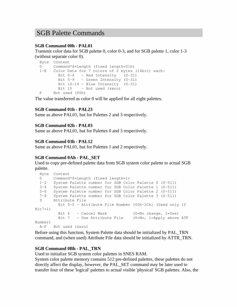
SGB Palette Commands SGB Command 00h - PAL01 Transmit color data for SGB palette 0, color 0-3, and for SGB palette 1, color 1-3 (without separate color 0). Byte Content 0 Command*8+Length (fixed length=01h) 1-E Color Data for 7 colors of 2 bytes (16bit) each: Bit 0-4 - Red Intensity (0-31) Bit 5-9 - Green Intensity (0-31) Bit 10-14 - Blue Intensity (0-31) Bit 15 - Not used (zero) F Not used (00h)
The value transferred as color 0 will be applied for all eight palettes. SGB Command 01h - PAL23 Same as above PAL01, but for Palettes 2 and 3 respectively. SGB Command 02h - PAL03 Same as above PAL01, but for Palettes 0 and 3 respectively. SGB Command 03h - PAL12 Same as above PAL01, but for Palettes 1 and 2 respectively. SGB Command 0Ah - PAL_SET Used to copy pre-defined palette data from SGB system color palette to actual SGB palette. Byte Content 0 Command*8+Length (fixed length=1) 1-2 System Palette number for SGB Color Palette 0 (0-511) 3-4 System Palette number for SGB Color Palette 1 (0-511) 5-6 System Palette number for SGB Color Palette 2 (0-511) 7-8 System Palette number for SGB Color Palette 3 (0-511) 9 Attribute File Bit 0-5 - Attribute File Number (00h-2Ch) (Used only if Bit7=1) Bit 6 - Cancel Mask (0=No change, 1=Yes) Bit 7 - Use Attribute File (0=No, 1=Apply above ATF Number) A-F Not used (zero)
Before using this function, System Palette data should be initialized by PAL_TRN command, and (when used) Attribute File data should be initialized by ATTR_TRN. SGB Command 0Bh - PAL_TRN Used to initialize SGB system color palettes in SNES RAM. System color palette memory contains 512 pre-defined palettes, these palettes do not directly affect the display, however, the PAL_SET command may be later used to transfer four of these 'logical' palettes to actual visible 'physical' SGB palettes. Also, the
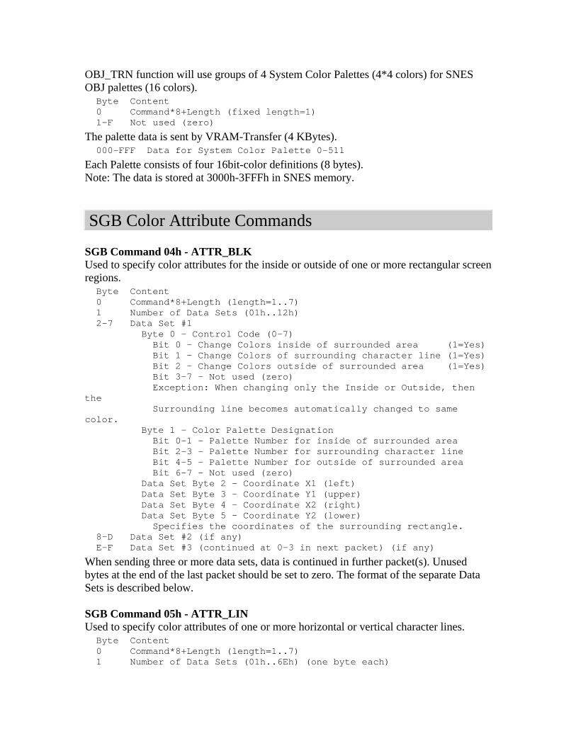
OBJ_TRN function will use groups of 4 System Color Palettes (4*4 colors) for SNES OBJ palettes (16 colors). Byte Content 0 Command*8+Length (fixed length=1) 1-F Not used (zero)
The palette data is sent by VRAM-Transfer (4 KBytes). 000-FFF Data for System Color Palette 0-511
Each Palette consists of four 16bit-color definitions (8 bytes). Note: The data is stored at 3000h-3FFFh in SNES memory.
SGB Color Attribute Commands SGB Command 04h - ATTR_BLK Used to specify color attributes for the inside or outside of one or more rectangular screen regions. Byte Content 0 Command*8+Length (length=1..7) 1 Number of Data Sets (01h..12h) 2-7 Data Set #1 Byte 0 - Control Code (0-7) Bit 0 - Change Colors inside of surrounded area (1=Yes) Bit 1 - Change Colors of surrounding character line (1=Yes) Bit 2 - Change Colors outside of surrounded area (1=Yes) Bit 3-7 - Not used (zero) Exception: When changing only the Inside or Outside, then the Surrounding line becomes automatically changed to same color. Byte 1 - Color Palette Designation Bit 0-1 - Palette Number for inside of surrounded area Bit 2-3 - Palette Number for surrounding character line Bit 4-5 - Palette Number for outside of surrounded area Bit 6-7 - Not used (zero) Data Set Byte 2 - Coordinate X1 (left) Data Set Byte 3 - Coordinate Y1 (upper) Data Set Byte 4 - Coordinate X2 (right) Data Set Byte 5 - Coordinate Y2 (lower) Specifies the coordinates of the surrounding rectangle. 8-D Data Set #2 (if any) E-F Data Set #3 (continued at 0-3 in next packet) (if any)
When sending three or more data sets, data is continued in further packet(s). Unused bytes at the end of the last packet should be set to zero. The format of the separate Data Sets is described below. SGB Command 05h - ATTR_LIN Used to specify color attributes of one or more horizontal or vertical character lines. Byte Content 0 Command*8+Length (length=1..7) 1 Number of Data Sets (01h..6Eh) (one byte each)
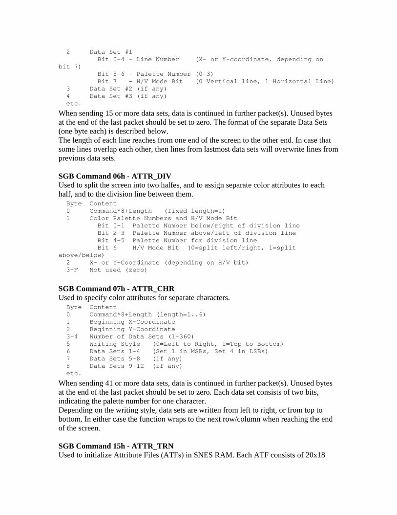
2 Data Set #1 Bit 0-4 - Line Number (X- or Y-coordinate, depending on bit 7) Bit 5-6 - Palette Number (0-3) Bit 7 - H/V Mode Bit (0=Vertical line, 1=Horizontal Line) 3 Data Set #2 (if any) 4 Data Set #3 (if any) etc.
When sending 15 or more data sets, data is continued in further packet(s). Unused bytes at the end of the last packet should be set to zero. The format of the separate Data Sets (one byte each) is described below. The length of each line reaches from one end of the screen to the other end. In case that some lines overlap each other, then lines from lastmost data sets will overwrite lines from previous data sets. SGB Command 06h - ATTR_DIV Used to split the screen into two halfes, and to assign separate color attributes to each half, and to the division line between them. Byte Content 0 Command*8+Length (fixed length=1) 1 Color Palette Numbers and H/V Mode Bit Bit 0-1 Palette Number below/right of division line Bit 2-3 Palette Number above/left of division line Bit 4-5 Palette Number for division line Bit 6 H/V Mode Bit (0=split left/right, 1=split above/below) 2 X- or Y-Coordinate (depending on H/V bit) 3-F Not used (zero)
SGB Command 07h - ATTR_CHR Used to specify color attributes for separate characters. Byte Content 0 Command*8+Length (length=1..6) 1 Beginning X-Coordinate 2 Beginning Y-Coordinate 3-4 Number of Data Sets (1-360) 5 Writing Style (0=Left to Right, 1=Top to Bottom) 6 Data Sets 1-4 (Set 1 in MSBs, Set 4 in LSBs) 7 Data Sets 5-8 (if any) 8 Data Sets 9-12 (if any) etc.
When sending 41 or more data sets, data is continued in further packet(s). Unused bytes at the end of the last packet should be set to zero. Each data set consists of two bits, indicating the palette number for one character. Depending on the writing style, data sets are written from left to right, or from top to bottom. In either case the function wraps to the next row/column when reaching the end of the screen. SGB Command 15h - ATTR_TRN Used to initialize Attribute Files (ATFs) in SNES RAM. Each ATF consists of 20x18
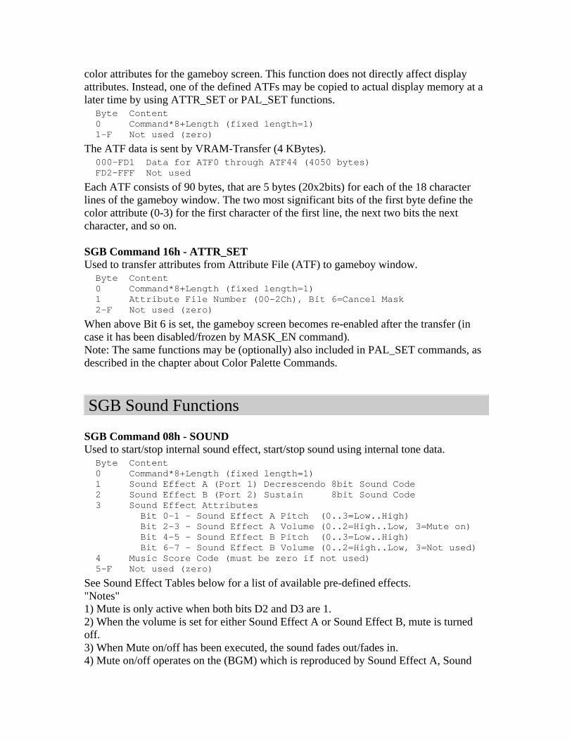
color attributes for the gameboy screen. This function does not directly affect display attributes. Instead, one of the defined ATFs may be copied to actual display memory at a later time by using ATTR_SET or PAL_SET functions. Byte Content 0 Command*8+Length (fixed length=1) 1-F Not used (zero)
The ATF data is sent by VRAM-Transfer (4 KBytes). 000-FD1 Data for ATF0 through ATF44 (4050 bytes) FD2-FFF Not used
Each ATF consists of 90 bytes, that are 5 bytes (20x2bits) for each of the 18 character lines of the gameboy window. The two most significant bits of the first byte define the color attribute (0-3) for the first character of the first line, the next two bits the next character, and so on. SGB Command 16h - ATTR_SET Used to transfer attributes from Attribute File (ATF) to gameboy window. Byte Content 0 Command*8+Length (fixed length=1) 1 Attribute File Number (00-2Ch), Bit 6=Cancel Mask 2-F Not used (zero)
When above Bit 6 is set, the gameboy screen becomes re-enabled after the transfer (in case it has been disabled/frozen by MASK_EN command). Note: The same functions may be (optionally) also included in PAL_SET commands, as described in the chapter about Color Palette Commands.
SGB Sound Functions SGB Command 08h - SOUND Used to start/stop internal sound effect, start/stop sound using internal tone data. Byte Content 0 Command*8+Length (fixed length=1) 1 Sound Effect A (Port 1) Decrescendo 8bit Sound Code 2 Sound Effect B (Port 2) Sustain 8bit Sound Code 3 Sound Effect Attributes Bit 0-1 - Sound Effect A Pitch (0..3=Low..High) Bit 2-3 - Sound Effect A Volume (0..2=High..Low, 3=Mute on) Bit 4-5 - Sound Effect B Pitch (0..3=Low..High) Bit 6-7 - Sound Effect B Volume (0..2=High..Low, 3=Not used) 4 Music Score Code (must be zero if not used) 5-F Not used (zero)
See Sound Effect Tables below for a list of available pre-defined effects. "Notes" 1) Mute is only active when both bits D2 and D3 are 1. 2) When the volume is set for either Sound Effect A or Sound Effect B, mute is turned off. 3) When Mute on/off has been executed, the sound fades out/fades in. 4) Mute on/off operates on the (BGM) which is reproduced by Sound Effect A, Sound
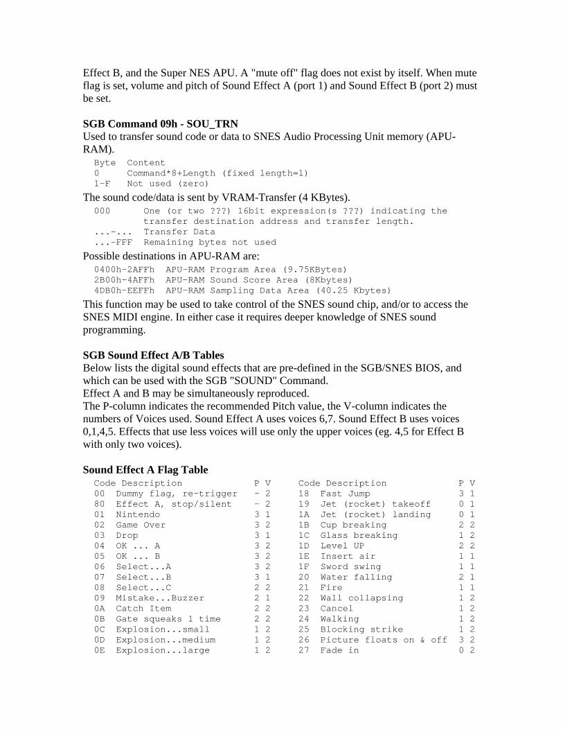
Effect B, and the Super NES APU. A "mute off" flag does not exist by itself. When mute flag is set, volume and pitch of Sound Effect A (port 1) and Sound Effect B (port 2) must be set. SGB Command 09h - SOU_TRN Used to transfer sound code or data to SNES Audio Processing Unit memory (APU-RAM). Byte Content 0 Command*8+Length (fixed length=1) 1-F Not used (zero)
The sound code/data is sent by VRAM-Transfer (4 KBytes). 000 One (or two ???) 16bit expression(s ???) indicating the transfer destination address and transfer length. ...-... Transfer Data ...-FFF Remaining bytes not used
Possible destinations in APU-RAM are: 0400h-2AFFh APU-RAM Program Area (9.75KBytes) 2B00h-4AFFh APU-RAM Sound Score Area (8Kbytes) 4DB0h-EEFFh APU-RAM Sampling Data Area (40.25 Kbytes)
This function may be used to take control of the SNES sound chip, and/or to access the SNES MIDI engine. In either case it requires deeper knowledge of SNES sound programming. SGB Sound Effect A/B Tables Below lists the digital sound effects that are pre-defined in the SGB/SNES BIOS, and which can be used with the SGB "SOUND" Command. Effect A and B may be simultaneously reproduced. The P-column indicates the recommended Pitch value, the V-column indicates the numbers of Voices used. Sound Effect A uses voices 6,7. Sound Effect B uses voices 0,1,4,5. Effects that use less voices will use only the upper voices (eg. 4,5 for Effect B with only two voices). Sound Effect A Flag Table Code Description P V Code Description P V 00 Dummy flag, re-trigger - 2 18 Fast Jump 3 1 80 Effect A, stop/silent - 2 19 Jet (rocket) takeoff 0 1 01 Nintendo 3 1 1A Jet (rocket) landing 0 1 02 Game Over 3 2 1B Cup breaking 2 2 03 Drop 3 1 1C Glass breaking 1 2 04 OK ... A 3 2 1D Level UP 2 2 05 OK ... B 3 2 1E Insert air 1 1 06 Select...A 3 2 1F Sword swing 1 1 07 Select...B 3 1 20 Water falling 2 1 08 Select...C 2 2 21 Fire 1 1 09 Mistake...Buzzer 2 1 22 Wall collapsing 1 2 0A Catch Item 2 2 23 Cancel 1 2 0B Gate squeaks 1 time 2 2 24 Walking 1 2 0C Explosion...small 1 2 25 Blocking strike 1 2 0D Explosion...medium 1 2 26 Picture floats on & off 3 2 0E Explosion...large 1 2 27 Fade in 0 2
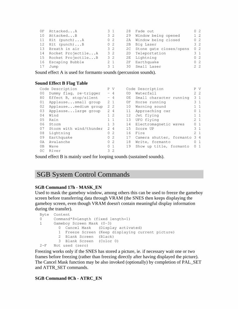
0F Attacked...A 3 1 28 Fade out 0 2 10 Attacked...B 3 2 29 Window being opened 1 2 11 Hit (punch)...A 0 2 2A Window being closed 0 2 12 Hit (punch)...B 0 2 2B Big Laser 3 2 13 Breath in air 3 2 2C Stone gate closes/opens 0 2 14 Rocket Projectile...A 3 2 2D Teleportation 3 1 15 Rocket Projectile...B 3 2 2E Lightning 0 2 16 Escaping Bubble 2 1 2F Earthquake 0 2 17 Jump 3 1 30 Small Laser 2 2
Sound effect A is used for formanto sounds (percussion sounds). Sound Effect B Flag Table Code Description P V Code Description P V 00 Dummy flag, re-trigger - 4 0D Waterfall 2 2 80 Effect B, stop/silent - 4 0E Small character running 3 1 01 Applause...small group 2 1 0F Horse running 3 1 02 Applause...medium group 2 2 10 Warning sound 1 1 03 Applause...large group 2 4 11 Approaching car 0 1 04 Wind 1 2 12 Jet flying 1 1 05 Rain 1 1 13 UFO flying 2 1 06 Storm 1 3 14 Electromagnetic waves 0 1 07 Storm with wind/thunder 2 4 15 Score UP 3 1 08 Lightning 0 2 16 Fire 2 1 09 Earthquake 0 2 17 Camera shutter, formanto 3 4 0A Avalanche 0 2 18 Write, formanto 0 1 0B Wave 0 1 19 Show up title, formanto 0 1 0C River 3 2
Sound effect B is mainly used for looping sounds (sustained sounds).
SGB System Control Commands SGB Command 17h - MASK_EN Used to mask the gameboy window, among others this can be used to freeze the gameboy screen before transferring data through VRAM (the SNES then keeps displaying the gameboy screen, even though VRAM doesn't contain meaningful display information during the transfer). Byte Content 0 Command*8+Length (fixed length=1) 1 Gameboy Screen Mask (0-3) 0 Cancel Mask (Display activated) 1 Freeze Screen (Keep displaying current picture) 2 Blank Screen (Black) 3 Blank Screen (Color 0) 2-F Not used (zero)
Freezing works only if the SNES has stored a picture, ie. if necessary wait one or two frames before freezing (rather than freezing directly after having displayed the picture). The Cancel Mask function may be also invoked (optionally) by completion of PAL_SET and ATTR_SET commands. SGB Command 0Ch - ATRC_EN
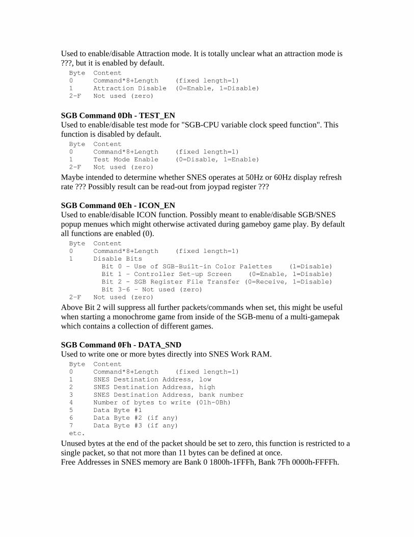
Used to enable/disable Attraction mode. It is totally unclear what an attraction mode is ???, but it is enabled by default. Byte Content 0 Command*8+Length (fixed length=1) 1 Attraction Disable (0=Enable, 1=Disable) 2-F Not used (zero)
SGB Command 0Dh - TEST_EN Used to enable/disable test mode for "SGB-CPU variable clock speed function". This function is disabled by default. Byte Content 0 Command*8+Length (fixed length=1) 1 Test Mode Enable (0=Disable, 1=Enable) 2-F Not used (zero)
Maybe intended to determine whether SNES operates at 50Hz or 60Hz display refresh rate ??? Possibly result can be read-out from joypad register ??? SGB Command 0Eh - ICON_EN Used to enable/disable ICON function. Possibly meant to enable/disable SGB/SNES popup menues which might otherwise activated during gameboy game play. By default all functions are enabled (0). Byte Content 0 Command*8+Length (fixed length=1) 1 Disable Bits Bit 0 - Use of SGB-Built-in Color Palettes (1=Disable) Bit 1 - Controller Set-up Screen (0=Enable, 1=Disable) Bit 2 - SGB Register File Transfer (0=Receive, 1=Disable) Bit 3-6 - Not used (zero) 2-F Not used (zero)
Above Bit 2 will suppress all further packets/commands when set, this might be useful when starting a monochrome game from inside of the SGB-menu of a multi-gamepak which contains a collection of different games. SGB Command 0Fh - DATA_SND Used to write one or more bytes directly into SNES Work RAM. Byte Content 0 Command*8+Length (fixed length=1) 1 SNES Destination Address, low 2 SNES Destination Address, high 3 SNES Destination Address, bank number 4 Number of bytes to write (01h-0Bh) 5 Data Byte #1 6 Data Byte #2 (if any) 7 Data Byte #3 (if any) etc.
Unused bytes at the end of the packet should be set to zero, this function is restricted to a single packet, so that not more than 11 bytes can be defined at once. Free Addresses in SNES memory are Bank 0 1800h-1FFFh, Bank 7Fh 0000h-FFFFh.
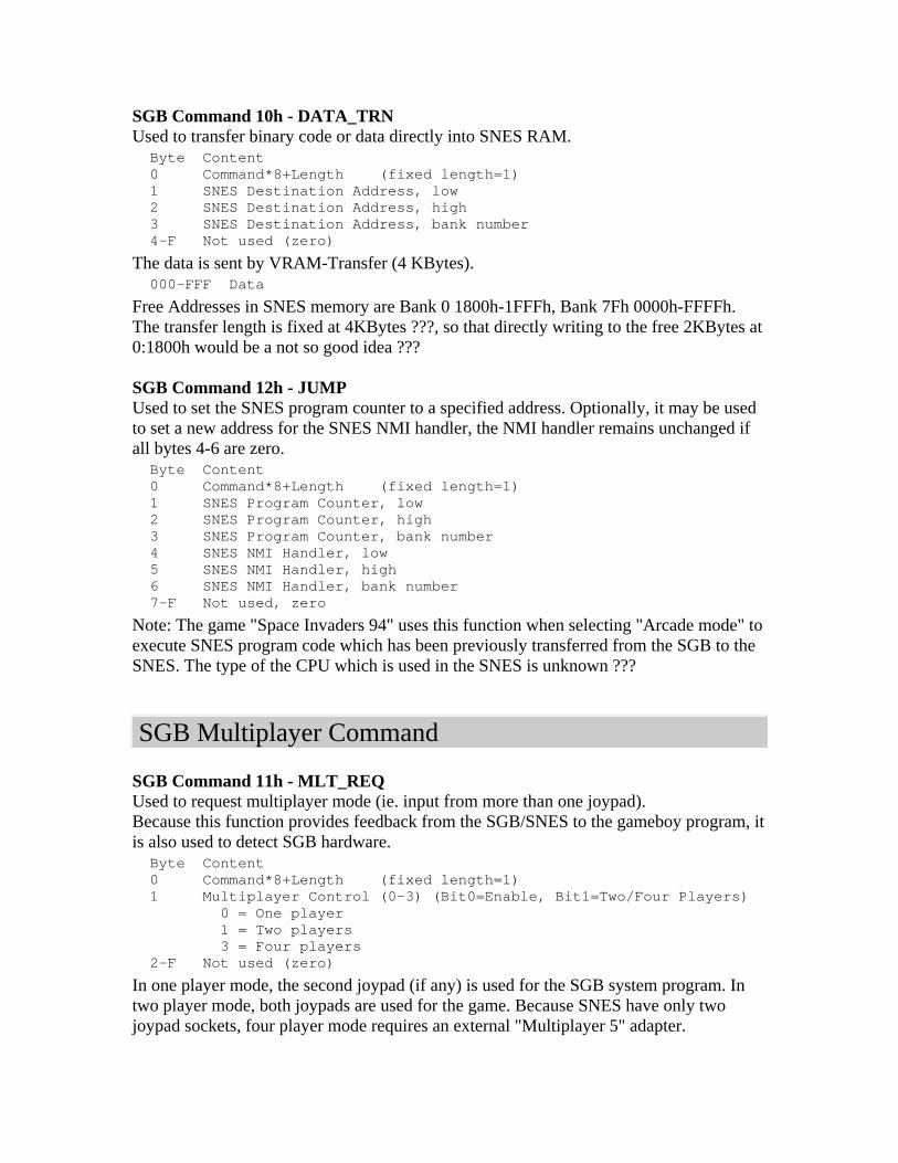
SGB Command 10h - DATA_TRN Used to transfer binary code or data directly into SNES RAM. Byte Content 0 Command*8+Length (fixed length=1) 1 SNES Destination Address, low 2 SNES Destination Address, high 3 SNES Destination Address, bank number 4-F Not used (zero)
The data is sent by VRAM-Transfer (4 KBytes). 000-FFF Data
Free Addresses in SNES memory are Bank 0 1800h-1FFFh, Bank 7Fh 0000h-FFFFh. The transfer length is fixed at 4KBytes ???, so that directly writing to the free 2KBytes at 0:1800h would be a not so good idea ??? SGB Command 12h - JUMP Used to set the SNES program counter to a specified address. Optionally, it may be used to set a new address for the SNES NMI handler, the NMI handler remains unchanged if all bytes 4-6 are zero. Byte Content 0 Command*8+Length (fixed length=1) 1 SNES Program Counter, low 2 SNES Program Counter, high 3 SNES Program Counter, bank number 4 SNES NMI Handler, low 5 SNES NMI Handler, high 6 SNES NMI Handler, bank number 7-F Not used, zero
Note: The game "Space Invaders 94" uses this function when selecting "Arcade mode" to execute SNES program code which has been previously transferred from the SGB to the SNES. The type of the CPU which is used in the SNES is unknown ???
SGB Multiplayer Command SGB Command 11h - MLT_REQ Used to request multiplayer mode (ie. input from more than one joypad). Because this function provides feedback from the SGB/SNES to the gameboy program, it is also used to detect SGB hardware. Byte Content 0 Command*8+Length (fixed length=1) 1 Multiplayer Control (0-3) (Bit0=Enable, Bit1=Two/Four Players) 0 = One player 1 = Two players 3 = Four players 2-F Not used (zero)
In one player mode, the second joypad (if any) is used for the SGB system program. In two player mode, both joypads are used for the game. Because SNES have only two joypad sockets, four player mode requires an external "Multiplayer 5" adapter.
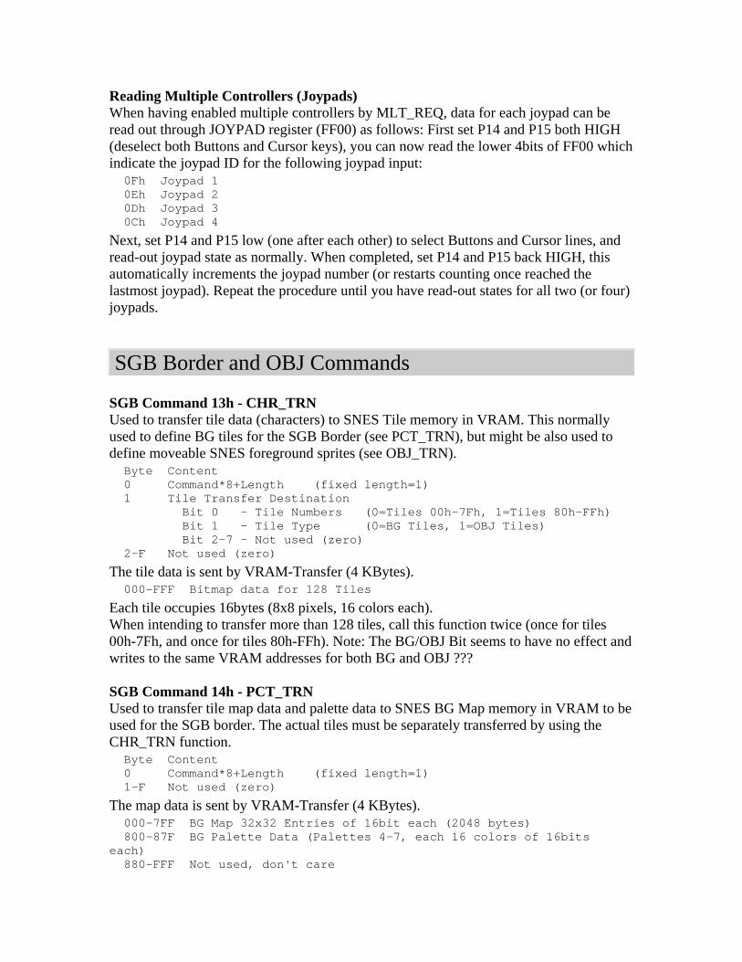
Reading Multiple Controllers (Joypads) When having enabled multiple controllers by MLT_REQ, data for each joypad can be read out through JOYPAD register (FF00) as follows: First set P14 and P15 both HIGH (deselect both Buttons and Cursor keys), you can now read the lower 4bits of FF00 which indicate the joypad ID for the following joypad input: 0Fh Joypad 1 0Eh Joypad 2 0Dh Joypad 3 0Ch Joypad 4
Next, set P14 and P15 low (one after each other) to select Buttons and Cursor lines, and read-out joypad state as normally. When completed, set P14 and P15 back HIGH, this automatically increments the joypad number (or restarts counting once reached the lastmost joypad). Repeat the procedure until you have read-out states for all two (or four) joypads.
SGB Border and OBJ Commands SGB Command 13h - CHR_TRN Used to transfer tile data (characters) to SNES Tile memory in VRAM. This normally used to define BG tiles for the SGB Border (see PCT_TRN), but might be also used to define moveable SNES foreground sprites (see OBJ_TRN). Byte Content 0 Command*8+Length (fixed length=1) 1 Tile Transfer Destination Bit 0 - Tile Numbers (0=Tiles 00h-7Fh, 1=Tiles 80h-FFh) Bit 1 - Tile Type (0=BG Tiles, 1=OBJ Tiles) Bit 2-7 - Not used (zero) 2-F Not used (zero)
The tile data is sent by VRAM-Transfer (4 KBytes). 000-FFF Bitmap data for 128 Tiles
Each tile occupies 16bytes (8x8 pixels, 16 colors each). When intending to transfer more than 128 tiles, call this function twice (once for tiles 00h-7Fh, and once for tiles 80h-FFh). Note: The BG/OBJ Bit seems to have no effect and writes to the same VRAM addresses for both BG and OBJ ??? SGB Command 14h - PCT_TRN Used to transfer tile map data and palette data to SNES BG Map memory in VRAM to be used for the SGB border. The actual tiles must be separately transferred by using the CHR_TRN function. Byte Content 0 Command*8+Length (fixed length=1) 1-F Not used (zero)
The map data is sent by VRAM-Transfer (4 KBytes). 000-7FF BG Map 32x32 Entries of 16bit each (2048 bytes) 800-87F BG Palette Data (Palettes 4-7, each 16 colors of 16bits each) 880-FFF Not used, don't care
Each BG Map Entry consists of a 16bit value as such: Bit 0-9 - Character Number (use only 00h-FFh, upper 2 bits zero) Bit 10-12 - Palette Number (use only 4-7, officially use only 4-6) Bit 13 - BG Priority (use only 0) Bit 14 - X-Flip (0=Normal, 1=Mirror horizontally) Bit 15 - Y-Flip (0=Normal, 1=Mirror vertically)
Even though 32x32 map entries are transferred, only upper 32x28 are actually used (256x224 pixels, SNES screen size). The 20x18 entries in the center of the 32x28 area should be set to 0000h as transparent space for the gameboy window to be displayed inside. Reportedly, non-transparent border data will cover the gameboy window. SGB Command 18h - OBJ_TRN Used to transfer OBJ attributes to SNES OAM memory. Unlike all other functions with the ending _TRN, this function does not use the usual one-shot 4KBytes VRAM transfer method. Instead, when enabled (below execute bit set), data is permanently (each frame) read out from the lower character line of the gameboy screen. To suppress garbage on the display, the lower line is masked, and only the upper 20x17 characters of the gameboy window are used - the masking method is unknwon - frozen, black, or recommended to be covered by the SGB border, or else ??? Also, when the function is enabled, "system attract mode is not performed" - whatever that means ??? Byte Content 0 Command*8+Length (fixed length=1) 1 Control Bits Bit 0 - SNES OBJ Mode enable (0=Cancel, 1=Enable) Bit 1 - Change OBJ Color (0=No, 1=Use definitions below) Bit 2-7 - Not used (zero) 2-3 System Color Palette Number for OBJ Palette 4 (0-511) 4-5 System Color Palette Number for OBJ Palette 5 (0-511) 6-7 System Color Palette Number for OBJ Palette 6 (0-511) 8-9 System Color Palette Number for OBJ Palette 7 (0-511) These color entries are ignored if above Control Bit 1 is zero. Because each OBJ palette consists of 16 colors, four system palette entries (of 4 colors each) are transferred into each OBJ palette. The system palette numbers are not required to be aligned to a multiple of four, and will wrap to palette number 0 when exceeding 511. For example, a value of 511 would copy system palettes 511, 0, 1, 2 to the SNES OBJ palette. A-F Not used (zero)
The recommended method is to "display" gameboy BG tiles F9h..FFh from left to right as first 7 characters of the bottom-most character line of the gameboy screen. As for normal 4KByte VRAM transfers, this area should not be scrolled, should not be overlapped by gameboy OBJs, and the gameboy BGP palette register should be set up properly. By following that method, SNES OAM data can be defined in the 70h bytes of the gameboy BG tile memory at following addresses: 8F90-8FEF SNES OAM, 24 Entries of 4 bytes each (96 bytes) 8FF0-8FF5 SNES OAM MSBs, 24 Entries of 2 bits each (6 bytes)
8FF6-8FFF Not used, don't care (10 bytes)
The format of SNES OAM Entries is: Byte 0 OBJ X-Position (0-511, MSB is separately stored, see below) Byte 1 OBJ Y-Position (0-255) Byte 2-3 Attributes (16bit) Bit 0-8 Tile Number (use only 00h-FFh, upper bit zero) Bit 9-11 Palette Number (use only 4-7) Bit 12-13 OBJ Priority (use only 3) Bit 14 X-Flip (0=Normal, 1=Mirror horizontally) Bit 15 Y-Flip (0=Normal, 1=Mirror vertically)
The format of SNES OAM MSB Entries is: Actually, the format is unknown ??? However, 2 bits are used per entry: One bit is the most significant bit of the OBJ X-Position. The other bit specifies the OBJ size (8x8 or 16x16 pixels).
CPU Registers and Flags Registers 16bit Hi Lo Name/Function AF A - Accumulator & Flags BC B C BC DE D E DE HL H L HL SP - - Stack Pointer PC - - Program Counter/Pointer
As shown above, most registers can be accessed either as one 16bit register, or as two separate 8bit registers. The Flag Register (lower 8bit of AF register) Bit Name Set Clr Expl. 7 zf Z NZ Zero Flag 6 n - - Add/Sub-Flag (BCD) 5 h - - Half Carry Flag (BCD) 4 cy C NC Carry Flag 3-0 - - - Not used (always zero)
Conatins the result from the recent instruction which has affected flags. The Zero Flag (Z) This bit becomes set (1) if the result of an operation has been zero (0). Used for conditional jumps. The Carry Flag (C, or Cy) Becomes set when the result of an addition became bigger than FFh (8bit) or FFFFh (16bit). Or when the result of a subtraction or comparision became less than zero (much as for Z80 and 80x86 CPUs, but unlike as for 65XX and ARM CPUs). Also the flag becomes set when a rotate/shift operation has shifted-out a "1"-bit. Used for conditional jumps, and for instructions such like ADC, SBC, RL, RLA, etc.
The BCD Flags (N, H) These flags are (rarely) used for the DAA instruction only, N Indicates whether the previous instruction has been an addition or subtraction, and H indicates carry for lower 4bits of the result, also for DAA, the C flag must indicate carry for upper 8bits. After adding/subtracting two BCD numbers, DAA is intended to convert the result into BCD format; BCD numbers are ranged from 00h to 99h rather than 00h to FFh. Because C and H flags must contain carry-outs for each digit, DAA cannot be used for 16bit operations (which have 4 digits), or for INC/DEC operations (which do not affect C-flag).
CPU Instruction Set Tables below specify the mnemonic, opcode bytes, clock cycles, affected flags (ordered as znhc), and explanatation. The timings assume a CPU clock frequency of 4.194304 MHz (or 8.4 MHz for CGB in double speed mode), as all gameboy timings are divideable by 4, many people specify timings and clock frequency divided by 4. GMB 8bit-Loadcommands ld r,r xx 4 ---- r=r ld r,n xx nn 8 ---- r=n ld r,(HL) xx 8 ---- r=(HL) ld (HL),r 7x 8 ---- (HL)=r ld (HL),n 36 nn 12 ---- ld A,(BC) 0A 8 ---- ld A,(DE) 1A 8 ---- ld A,(nn) FA 16 ---- ld (BC),A 02 8 ---- ld (DE),A 12 8 ---- ld (nn),A EA 16 ---- ld A,(FF00+n) F0 nn 12 ---- read from io-port n (memory FF00+n) ld (FF00+n),A E0 nn 12 ---- write to io-port n (memory FF00+n) ld A,(FF00+C) F2 8 ---- read from io-port C (memory FF00+C) ld (FF00+C),A E2 8 ---- write to io-port C (memory FF00+C) ldi (HL),A 22 8 ---- (HL)=A, HL=HL+1 ldi A,(HL) 2A 8 ---- A=(HL), HL=HL+1 ldd (HL),A 32 8 ---- (HL)=A, HL=HL-1 ldd A,(HL) 3A 8 ---- A=(HL), HL=HL-1
GMB 16bit-Loadcommands ld rr,nn x1 nn nn 12 ---- rr=nn (rr may be BC,DE,HL or SP) ld SP,HL F9 8 ---- SP=HL push rr x5 16 ---- SP=SP-2 (SP)=rr (rr may be BC,DE,HL,AF) pop rr x1 12 (AF) rr=(SP) SP=SP+2 (rr may be BC,DE,HL,AF)
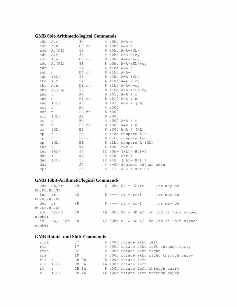
GMB 8bit-Arithmetic/logical Commands add A,r 8x 4 z0hc A=A+r add A,n C6 nn 8 z0hc A=A+n add A,(HL) 86 8 z0hc A=A+(HL) adc A,r 8x 4 z0hc A=A+r+cy adc A,n CE nn 8 z0hc A=A+n+cy adc A,(HL) 8E 8 z0hc A=A+(HL)+cy sub r 9x 4 z1hc A=A-r sub n D6 nn 8 z1hc A=A-n sub (HL) 96 8 z1hc A=A-(HL) sbc A,r 9x 4 z1hc A=A-r-cy sbc A,n DE nn 8 z1hc A=A-n-cy sbc A,(HL) 9E 8 z1hc A=A-(HL)-cy and r Ax 4 z010 A=A & r and n E6 nn 8 z010 A=A & n and (HL) A6 8 z010 A=A & (HL) xor r Ax 4 z000 xor n EE nn 8 z000 xor (HL) AE 8 z000 or r Bx 4 z000 A=A | r or n F6 nn 8 z000 A=A | n or (HL) B6 8 z000 A=A | (HL) cp r Bx 4 z1hc compare A-r cp n FE nn 8 z1hc compare A-n cp (HL) BE 8 z1hc compare A-(HL) inc r xx 4 z0h- r=r+1 inc (HL) 34 12 z0h- (HL)=(HL)+1 dec r xx 4 z1h- r=r-1 dec (HL) 35 12 z1h- (HL)=(HL)-1 daa 27 4 z-0x decimal adjust akku cpl 2F 4 -11- A = A xor FF
GMB 16bit-Arithmetic/logical Commands add HL,rr x9 8 -0hc HL = HL+rr ;rr may be BC,DE,HL,SP inc rr x3 8 ---- rr = rr+1 ;rr may be BC,DE,HL,SP dec rr xB 8 ---- rr = rr-1 ;rr may be BC,DE,HL,SP add SP,dd E8 16 00hc SP = SP +/- dd ;dd is 8bit signed number ld HL,SP+dd F8 12 00hc HL = SP +/- dd ;dd is 8bit signed number
GMB Rotate- und Shift-Commands rlca 07 4 000c rotate akku left rla 17 4 000c rotate akku left through carry rrca 0F 4 000c rotate akku right rra 1F 4 000c rotate akku right through carry rlc r CB 0x 8 z00c rotate left rlc (HL) CB 06 16 z00c rotate left rl r CB 1x 8 z00c rotate left through carry rl (HL) CB 16 16 z00c rotate left through carry
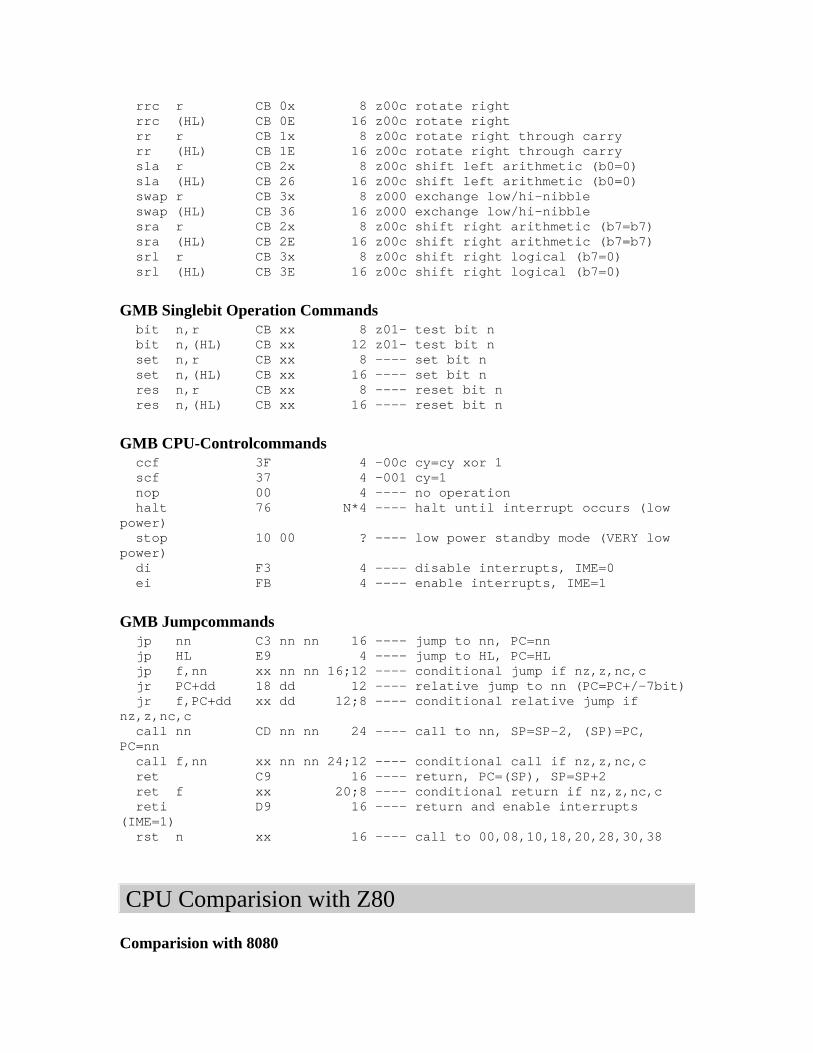
rrc r CB 0x 8 z00c rotate right rrc (HL) CB 0E 16 z00c rotate right rr r CB 1x 8 z00c rotate right through carry rr (HL) CB 1E 16 z00c rotate right through carry sla r CB 2x 8 z00c shift left arithmetic (b0=0) sla (HL) CB 26 16 z00c shift left arithmetic (b0=0) swap r CB 3x 8 z000 exchange low/hi-nibble swap (HL) CB 36 16 z000 exchange low/hi-nibble sra r CB 2x 8 z00c shift right arithmetic (b7=b7) sra (HL) CB 2E 16 z00c shift right arithmetic (b7=b7) srl r CB 3x 8 z00c shift right logical (b7=0) srl (HL) CB 3E 16 z00c shift right logical (b7=0)
GMB Singlebit Operation Commands bit n,r CB xx 8 z01- test bit n bit n,(HL) CB xx 12 z01- test bit n set n,r CB xx 8 ---- set bit n set n,(HL) CB xx 16 ---- set bit n res n,r CB xx 8 ---- reset bit n res n,(HL) CB xx 16 ---- reset bit n
GMB CPU-Controlcommands ccf 3F 4 -00c cy=cy xor 1 scf 37 4 -001 cy=1 nop 00 4 ---- no operation halt 76 N*4 ---- halt until interrupt occurs (low power) stop 10 00 ? ---- low power standby mode (VERY low power) di F3 4 ---- disable interrupts, IME=0 ei FB 4 ---- enable interrupts, IME=1
GMB Jumpcommands jp nn C3 nn nn 16 ---- jump to nn, PC=nn jp HL E9 4 ---- jump to HL, PC=HL jp f,nn xx nn nn 16;12 ---- conditional jump if nz,z,nc,c jr PC+dd 18 dd 12 ---- relative jump to nn (PC=PC+/-7bit) jr f,PC+dd xx dd 12;8 ---- conditional relative jump if nz,z,nc,c call nn CD nn nn 24 ---- call to nn, SP=SP-2, (SP)=PC, PC=nn call f,nn xx nn nn 24;12 ---- conditional call if nz,z,nc,c ret C9 16 ---- return, PC=(SP), SP=SP+2 ret f xx 20;8 ---- conditional return if nz,z,nc,c reti D9 16 ---- return and enable interrupts (IME=1) rst n xx 16 ---- call to 00,08,10,18,20,28,30,38
CPU Comparision with Z80 Comparision with 8080
Basically, the gameboy CPU works more like an older 8080 CPU rather than like a more powerful Z80 CPU. It is, however, supporting CB-prefixed instructions. Also, all known gameboy assemblers using the more obvious Z80-style syntax, rather than the chaotic 8080-style syntax. Comparision with Z80 Any DD-, ED-, and FD-prefixed instructions are missing, that means no IX-, IY-registers, no block commands, and some other missing commands. All exchange instructions have been removed (including total absence of second register set), 16bit memory accesses are mostly missing, and 16bit arithmetic functions are heavily cut-down. The gameboy has no IN/OUT instructions, instead I/O ports are accessed directly by normal LD instructions, or by special LD (FF00+n) opcodes. The sign and parity/overflow flags have been removed. The gameboy operates approximately as fast as a 4MHz Z80 (8MHz in CGB double speed mode), execution time of all instructions has been rounded up to a multiple of 4 cycles though. Moved, Removed, and Added Opcodes Opcode Z80 GMB --------------------------------------- 08 EX AF,AF LD (nn),SP 10 DJNZ PC+dd STOP 22 LD (nn),HL LDI (HL),A 2A LD HL,(nn) LDI A,(HL) 32 LD (nn),A LDD (HL),A 3A LD A,(nn) LDD A,(HL) D3 OUT (n),A - D9 EXX RETI DB IN A,(n) - DD <IX> - E0 RET PO LD (FF00+n),A E2 JP PO,nn LD (FF00+C),A E3 EX (SP),HL - E4 CALL P0,nn - E8 RET PE ADD SP,dd EA JP PE,nn LD (nn),A EB EX DE,HL - EC CALL PE,nn - ED <pref> - F0 RET P LD A,(FF00+n) F2 JP P,nn LD A,(FF00+C) F4 CALL P,nn - F8 RET M LD HL,SP+dd FA JP M,nn LD A,(nn) FC CALL M,nn - FD <IY> - CB3X SLL r/(HL) SWAP r/(HL)
Note: The unused (-) opcodes will lock-up the gameboy CPU when used.
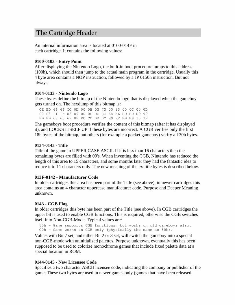
The Cartridge Header An internal information area is located at 0100-014F in each cartridge. It contains the following values: 0100-0103 - Entry Point After displaying the Nintendo Logo, the built-in boot procedure jumps to this address (100h), which should then jump to the actual main program in the cartridge. Usually this 4 byte area contains a NOP instruction, followed by a JP 0150h instruction. But not always. 0104-0133 - Nintendo Logo These bytes define the bitmap of the Nintendo logo that is displayed when the gameboy gets turned on. The hexdump of this bitmap is: CE ED 66 66 CC 0D 00 0B 03 73 00 83 00 0C 00 0D 00 08 11 1F 88 89 00 0E DC CC 6E E6 DD DD D9 99 BB BB 67 63 6E 0E EC CC DD DC 99 9F BB B9 33 3E
The gameboys boot procedure verifies the content of this bitmap (after it has displayed it), and LOCKS ITSELF UP if these bytes are incorrect. A CGB verifies only the first 18h bytes of the bitmap, but others (for example a pocket gameboy) verify all 30h bytes. 0134-0143 - Title Title of the game in UPPER CASE ASCII. If it is less than 16 characters then the remaining bytes are filled with 00's. When inventing the CGB, Nintendo has reduced the length of this area to 15 characters, and some months later they had the fantastic idea to reduce it to 11 characters only. The new meaning of the ex-title bytes is described below. 013F-0142 - Manufacturer Code In older cartridges this area has been part of the Title (see above), in newer cartridges this area contains an 4 character uppercase manufacturer code. Purpose and Deeper Meaning unknown. 0143 - CGB Flag In older cartridges this byte has been part of the Title (see above). In CGB cartridges the upper bit is used to enable CGB functions. This is required, otherwise the CGB switches itself into Non-CGB-Mode. Typical values are: 80h - Game supports CGB functions, but works on old gameboys also. C0h - Game works on CGB only (physically the same as 80h).
Values with Bit 7 set, and either Bit 2 or 3 set, will switch the gameboy into a special non-CGB-mode with uninitialized palettes. Purpose unknown, eventually this has been supposed to be used to colorize monochrome games that include fixed palette data at a special location in ROM. 0144-0145 - New Licensee Code Specifies a two character ASCII licensee code, indicating the company or publisher of the game. These two bytes are used in newer games only (games that have been released
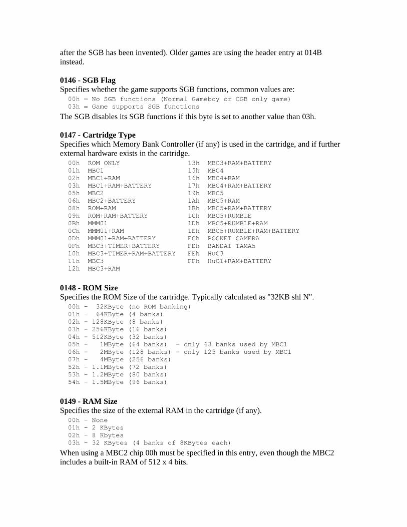
after the SGB has been invented). Older games are using the header entry at 014B instead. 0146 - SGB Flag Specifies whether the game supports SGB functions, common values are: 00h = No SGB functions (Normal Gameboy or CGB only game) 03h = Game supports SGB functions
The SGB disables its SGB functions if this byte is set to another value than 03h. 0147 - Cartridge Type Specifies which Memory Bank Controller (if any) is used in the cartridge, and if further external hardware exists in the cartridge. 00h ROM ONLY 13h MBC3+RAM+BATTERY 01h MBC1 15h MBC4 02h MBC1+RAM 16h MBC4+RAM 03h MBC1+RAM+BATTERY 17h MBC4+RAM+BATTERY 05h MBC2 19h MBC5 06h MBC2+BATTERY 1Ah MBC5+RAM 08h ROM+RAM 1Bh MBC5+RAM+BATTERY 09h ROM+RAM+BATTERY 1Ch MBC5+RUMBLE 0Bh MMM01 1Dh MBC5+RUMBLE+RAM 0Ch MMM01+RAM 1Eh MBC5+RUMBLE+RAM+BATTERY 0Dh MMM01+RAM+BATTERY FCh POCKET CAMERA 0Fh MBC3+TIMER+BATTERY FDh BANDAI TAMA5 10h MBC3+TIMER+RAM+BATTERY FEh HuC3 11h MBC3 FFh HuC1+RAM+BATTERY 12h MBC3+RAM
0148 - ROM Size Specifies the ROM Size of the cartridge. Typically calculated as "32KB shl N". 00h - 32KByte (no ROM banking) 01h - 64KByte (4 banks) 02h - 128KByte (8 banks) 03h - 256KByte (16 banks) 04h - 512KByte (32 banks) 05h - 1MByte (64 banks) - only 63 banks used by MBC1 06h - 2MByte (128 banks) - only 125 banks used by MBC1 07h - 4MByte (256 banks) 52h - 1.1MByte (72 banks) 53h - 1.2MByte (80 banks) 54h - 1.5MByte (96 banks)
0149 - RAM Size Specifies the size of the external RAM in the cartridge (if any). 00h - None 01h - 2 KBytes 02h - 8 Kbytes 03h - 32 KBytes (4 banks of 8KBytes each)
When using a MBC2 chip 00h must be specified in this entry, even though the MBC2 includes a built-in RAM of 512 x 4 bits.
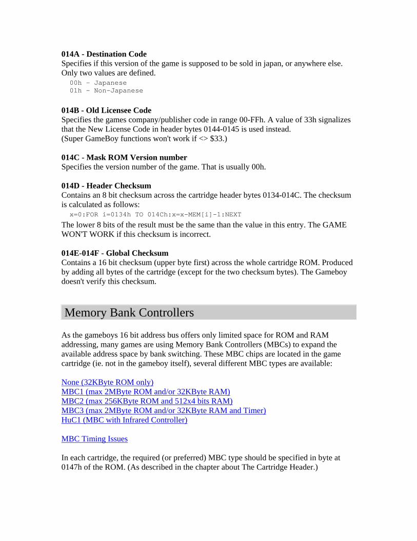
014A - Destination Code Specifies if this version of the game is supposed to be sold in japan, or anywhere else. Only two values are defined. 00h - Japanese 01h - Non-Japanese
014B - Old Licensee Code Specifies the games company/publisher code in range 00-FFh. A value of 33h signalizes that the New License Code in header bytes 0144-0145 is used instead. (Super GameBoy functions won't work if <> $33.) 014C - Mask ROM Version number Specifies the version number of the game. That is usually 00h. 014D - Header Checksum Contains an 8 bit checksum across the cartridge header bytes 0134-014C. The checksum is calculated as follows: x=0:FOR i=0134h TO 014Ch:x=x-MEM[i]-1:NEXT
The lower 8 bits of the result must be the same than the value in this entry. The GAME WON'T WORK if this checksum is incorrect. 014E-014F - Global Checksum Contains a 16 bit checksum (upper byte first) across the whole cartridge ROM. Produced by adding all bytes of the cartridge (except for the two checksum bytes). The Gameboy doesn't verify this checksum.
Memory Bank Controllers As the gameboys 16 bit address bus offers only limited space for ROM and RAM addressing, many games are using Memory Bank Controllers (MBCs) to expand the available address space by bank switching. These MBC chips are located in the game cartridge (ie. not in the gameboy itself), several different MBC types are available: None (32KByte ROM only) MBC1 (max 2MByte ROM and/or 32KByte RAM) MBC2 (max 256KByte ROM and 512x4 bits RAM) MBC3 (max 2MByte ROM and/or 32KByte RAM and Timer) HuC1 (MBC with Infrared Controller) MBC Timing Issues In each cartridge, the required (or preferred) MBC type should be specified in byte at 0147h of the ROM. (As described in the chapter about The Cartridge Header.)
None (32KByte ROM only) Small games of not more than 32KBytes ROM do not require a MBC chip for ROM banking. The ROM is directly mapped to memory at 0000-7FFFh. Optionally up to 8KByte of RAM could be connected at A000-BFFF, even though that could require a tiny MBC-like circuit, but no real MBC chip.
MBC1 (max 2MByte ROM and/or 32KByte RAM) This is the first MBC chip for the gameboy. Any newer MBC chips are working similiar, so that is relative easy to upgrade a program from one MBC chip to another - or even to make it compatible to several different types of MBCs. Note that the memory in range 0000-7FFF is used for both reading from ROM, and for writing to the MBCs Control Registers. 0000-3FFF - ROM Bank 00 (Read Only) This area always contains the first 16KBytes of the cartridge ROM. 4000-7FFF - ROM Bank 01-7F (Read Only) This area may contain any of the further 16KByte banks of the ROM, allowing to address up to 125 ROM Banks (almost 2MByte). As described below, bank numbers 20h, 40h, and 60h cannot be used, resulting in the odd amount of 125 banks. A000-BFFF - RAM Bank 00-03, if any (Read/Write) This area is used to address external RAM in the cartridge (if any). External RAM is often battery buffered, allowing to store game positions or high score tables, even if the gameboy is turned off, or if the cartridge is removed from the gameboy. Available RAM sizes are: 2KByte (at A000-A7FF), 8KByte (at A000-BFFF), and 32KByte (in form of four 8K banks at A000-BFFF). 0000-1FFF - RAM Enable (Write Only) Before external RAM can be read or written, it must be enabled by writing to this address space. It is recommended to disable external RAM after accessing it, in order to protect its contents from damage during power down of the gameboy. Usually the following values are used: 00h Disable RAM (default) 0Ah Enable RAM
Practically any value with 0Ah in the lower 4 bits enables RAM, and any other value disables RAM. 2000-3FFF - ROM Bank Number (Write Only) Writing to this address space selects the lower 5 bits of the ROM Bank Number (in range 01-1Fh). When 00h is written, the MBC translates that to bank 01h also. That doesn't
harm so far, because ROM Bank 00h can be always directly accessed by reading from 0000-3FFF. But (when using the register below to specify the upper ROM Bank bits), the same happens for Bank 20h, 40h, and 60h. Any attempt to address these ROM Banks will select Bank 21h, 41h, and 61h instead. 4000-5FFF - RAM Bank Number - or - Upper Bits of ROM Bank Number (Write Only) This 2bit register can be used to select a RAM Bank in range from 00-03h, or to specify the upper two bits (Bit 5-6) of the ROM Bank number, depending on the current ROM/RAM Mode. (See below.) 6000-7FFF - ROM/RAM Mode Select (Write Only) This 1bit Register selects whether the two bits of the above register should be used as upper two bits of the ROM Bank, or as RAM Bank Number. 00h = ROM Banking Mode (up to 8KByte RAM, 2MByte ROM) (default) 01h = RAM Banking Mode (up to 32KByte RAM, 512KByte ROM)
The program may freely switch between both modes, the only limitiation is that only RAM Bank 00h can be used during Mode 0, and only ROM Banks 00-1Fh can be used during Mode 1.
MBC2 (max 256KByte ROM and 512x4 bits RAM) 0000-3FFF - ROM Bank 00 (Read Only) Same as for MBC1. 4000-7FFF - ROM Bank 01-0F (Read Only) Same as for MBC1, but only a total of 16 ROM banks is supported. A000-A1FF - 512x4bits RAM, built-in into the MBC2 chip (Read/Write) The MBC2 doesn't support external RAM, instead it includes 512x4 bits of built-in RAM (in the MBC2 chip itself). It still requires an external battery to save data during power-off though. As the data consists of 4bit values, only the lower 4 bits of the "bytes" in this memory area are used. 0000-1FFF - RAM Enable (Write Only) The least significant bit of the upper address byte must be zero to enable/disable cart RAM. For example the following addresses can be used to enable/disable cart RAM: 0000-00FF, 0200-02FF, 0400-04FF, ..., 1E00-1EFF. The suggested address range to use for MBC2 ram enable/disable is 0000-00FF. 2000-3FFF - ROM Bank Number (Write Only) Writing a value (XXXXBBBB - X = Don't cares, B = bank select bits) into 2000-3FFF area will select an appropriate ROM bank at 4000-7FFF.

The least significant bit of the upper address byte must be one to select a ROM bank. For example the following addresses can be used to select a ROM bank: 2100-21FF, 2300-23FF, 2500-25FF, ..., 3F00-3FFF. The suggested address range to use for MBC2 rom bank selection is 2100-21FF.
MBC3 (max 2MByte ROM and/or 32KByte RAM and Timer) Beside for the ability to access up to 2MB ROM (128 banks), and 32KB RAM (4 banks), the MBC3 also includes a built-in Real Time Clock (RTC). The RTC requires an external 32.768 kHz Quartz Oscillator, and an external battery (if it should continue to tick when the gameboy is turned off). 0000-3FFF - ROM Bank 00 (Read Only) Same as for MBC1. 4000-7FFF - ROM Bank 01-7F (Read Only) Same as for MBC1, except that accessing banks 20h, 40h, and 60h is supported now. A000-BFFF - RAM Bank 00-03, if any (Read/Write) A000-BFFF - RTC Register 08-0C (Read/Write) Depending on the current Bank Number/RTC Register selection (see below), this memory space is used to access an 8KByte external RAM Bank, or a single RTC Register. 0000-1FFF - RAM and Timer Enable (Write Only) Mostly the same as for MBC1, a value of 0Ah will enable reading and writing to external RAM - and to the RTC Registers! A value of 00h will disable either. 2000-3FFF - ROM Bank Number (Write Only) Same as for MBC1, except that the whole 7 bits of the RAM Bank Number are written directly to this address. As for the MBC1, writing a value of 00h, will select Bank 01h instead. All other values 01-7Fh select the corresponding ROM Banks. 4000-5FFF - RAM Bank Number - or - RTC Register Select (Write Only) As for the MBC1s RAM Banking Mode, writing a value in range for 00h-03h maps the corresponding external RAM Bank (if any) into memory at A000-BFFF. When writing a value of 08h-0Ch, this will map the corresponding RTC register into memory at A000-BFFF. That register could then be read/written by accessing any address in that area, typically that is done by using address A000. 6000-7FFF - Latch Clock Data (Write Only) When writing 00h, and then 01h to this register, the current time becomes latched into the RTC registers. The latched data will not change until it becomes latched again, by

repeating the write 00h->01h procedure. This is supposed for <reading> from the RTC registers. It is proof to read the latched (frozen) time from the RTC registers, while the clock itself continues to tick in background. The Clock Counter Registers 08h RTC S Seconds 0-59 (0-3Bh) 09h RTC M Minutes 0-59 (0-3Bh) 0Ah RTC H Hours 0-23 (0-17h) 0Bh RTC DL Lower 8 bits of Day Counter (0-FFh) 0Ch RTC DH Upper 1 bit of Day Counter, Carry Bit, Halt Flag Bit 0 Most significant bit of Day Counter (Bit 8) Bit 6 Halt (0=Active, 1=Stop Timer) Bit 7 Day Counter Carry Bit (1=Counter Overflow)
The Halt Flag is supposed to be set before <writing> to the RTC Registers. The Day Counter The total 9 bits of the Day Counter allow to count days in range from 0-511 (0-1FFh). The Day Counter Carry Bit becomes set when this value overflows. In that case the Carry Bit remains set until the program does reset it. Note that you can store an offset to the Day Counter in battery RAM. For example, every time you read a non-zero Day Counter, add this Counter to the offset in RAM, and reset the Counter to zero. This method allows to count any number of days, making your program Year-10000-Proof, provided that the cartridge gets used at least every 511 days. Delays When accessing the RTC Registers it is recommended to execute a 4ms delay (4 Cycles in Normal Speed Mode) between the separate accesses.
HuC1 (MBC with Infrared Controller) This controller (made by Hudson Soft) appears to be very similar to an MBC1 with the main difference being that it supports infrared LED input / output. (Similiar to the infrared port that has been later invented in CGBs.) The Japanese cart "Fighting Phoenix" (internal cart name: SUPER B DAMAN) is known to contain this chip.
MBC Timing Issues Using MBCs with CGB Double Speed Mode The MBC5 has been designed to support CGB Double Speed Mode. There have been rumours that older MBCs (like MBC1-3) wouldn't be fast enough in that mode. If so, it might be nethertheless possible to use Double Speed during periods which
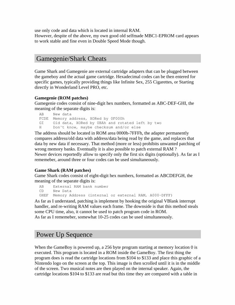
use only code and data which is located in internal RAM. However, despite of the above, my own good old selfmade MBC1-EPROM card appears to work stable and fine even in Double Speed Mode though.
Gamegenie/Shark Cheats Game Shark and Gamegenie are external cartridge adapters that can be plugged between the gameboy and the actual game cartridge. Hexadecimal codes can be then entered for specific games, typically providing things like Infinite Sex, 255 Cigarettes, or Starting directly in Wonderland Level PRO, etc. Gamegenie (ROM patches) Gamegenie codes consist of nine-digit hex numbers, formatted as ABC-DEF-GHI, the meaning of the separate digits is: AB New data FCDE Memory address, XORed by 0F000h GI Old data, XORed by 0BAh and rotated left by two H Don't know, maybe checksum and/or else
The address should be located in ROM area 0000h-7FFFh, the adapter permanently compares address/old data with address/data being read by the game, and replaces that data by new data if necessary. That method (more or less) prohibits unwanted patching of wrong memory banks. Eventually it is also possible to patch external RAM ? Newer devices reportedly allow to specify only the first six digits (optionally). As far as I rememeber, around three or four codes can be used simultaneously. Game Shark (RAM patches) Game Shark codes consist of eight-digit hex numbers, formatted as ABCDEFGH, the meaning of the separate digits is: AB External RAM bank number CD New Data GHEF Memory Address (internal or external RAM, A000-DFFF)
As far as I understand, patching is implement by hooking the original VBlank interrupt handler, and re-writing RAM values each frame. The downside is that this method steals some CPU time, also, it cannot be used to patch program code in ROM. As far as I rememeber, somewhat 10-25 codes can be used simultaneously.
Power Up Sequence When the GameBoy is powered up, a 256 byte program starting at memory location 0 is executed. This program is located in a ROM inside the GameBoy. The first thing the program does is read the cartridge locations from $104 to $133 and place this graphic of a Nintendo logo on the screen at the top. This image is then scrolled until it is in the middle of the screen. Two musical notes are then played on the internal speaker. Again, the cartridge locations $104 to $133 are read but this time they are compared with a table in
the internal rom. If any byte fails to compare, then the GameBoy stops comparing bytes and simply halts all operations. If all locations compare the same, then the GameBoy starts adding all of the bytes in the cartridge from $134 to $14d. A value of 25 decimal is added to this total. If the least significant byte of the result is a not a zero, then the GameBoy will stop doing anything. If it is a zero, then the internal ROM is disabled and cartridge program execution begins at location $100 with the following register values:
AF=$01B0 BC=$0013 DE=$00D8 HL=$014D Stack Pointer=$FFFE [$FF05] = $00 ; TIMA [$FF06] = $00 ; TMA [$FF07] = $00 ; TAC [$FF10] = $80 ; NR10 [$FF11] = $BF ; NR11 [$FF12] = $F3 ; NR12 [$FF14] = $BF ; NR14 [$FF16] = $3F ; NR21 [$FF17] = $00 ; NR22 [$FF19] = $BF ; NR24 [$FF1A] = $7F ; NR30 [$FF1B] = $FF ; NR31 [$FF1C] = $9F ; NR32 [$FF1E] = $BF ; NR33 [$FF20] = $FF ; NR41 [$FF21] = $00 ; NR42 [$FF22] = $00 ; NR43 [$FF23] = $BF ; NR30 [$FF24] = $77 ; NR50 [$FF25] = $F3 ; NR51 [$FF26] = $F1-GB, $F0-SGB ; NR52 [$FF40] = $91 ; LCDC [$FF42] = $00 ; SCY [$FF43] = $00 ; SCX [$FF45] = $00 ; LYC [$FF47] = $FC ; BGP [$FF48] = $FF ; OBP0 [$FF49] = $FF ; OBP1 [$FF4A] = $00 ; WY [$FF4B] = $00 ; WX [$FFFF] = $00 ; IE
It is not a good idea to assume the above values will always exist. A later version GameBoy could contain different values than these at reset. Always set these registers on reset rather than assume they are as above. Please note that GameBoy internal RAM on power up contains random data. All of the GameBoy emulators tend to set all RAM to value $00 on entry. Cart RAM the first time it is accessed on a real GameBoy contains random data. It will
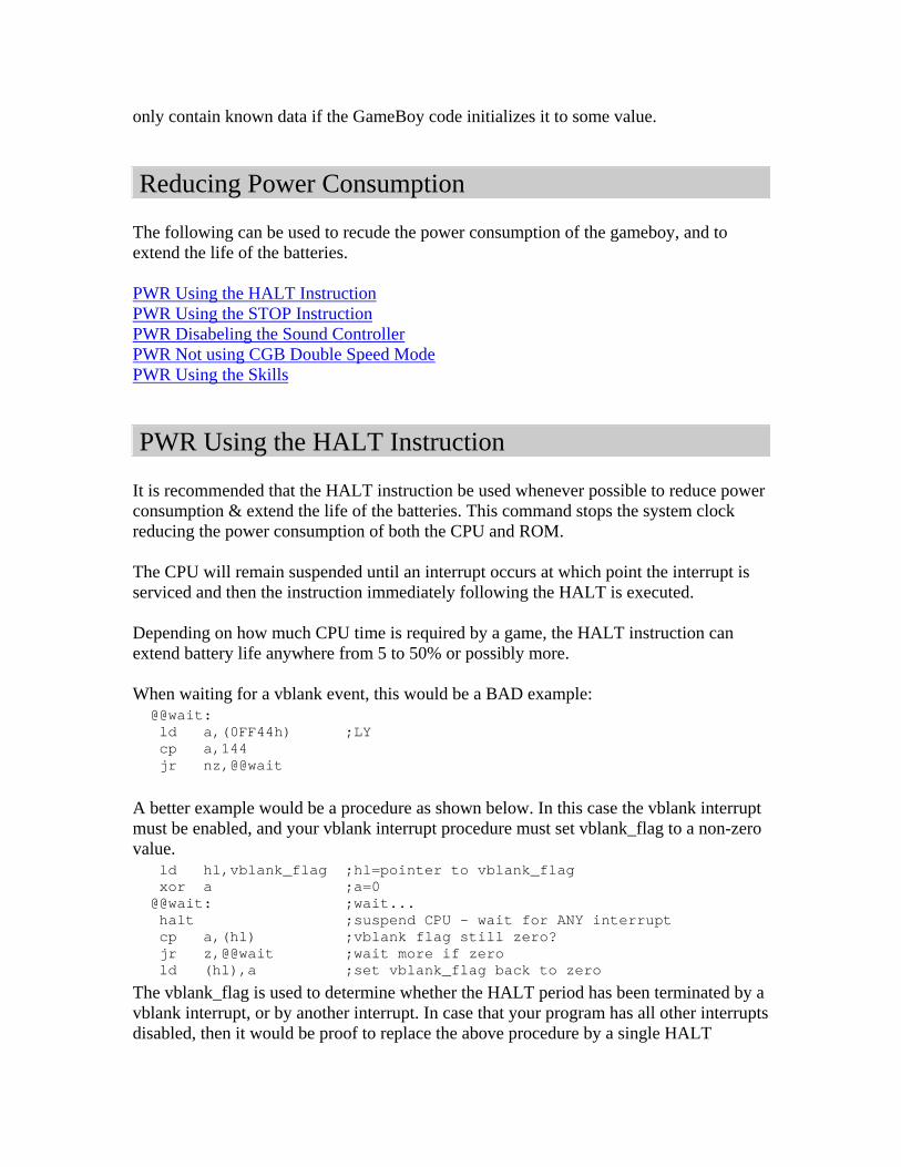
only contain known data if the GameBoy code initializes it to some value.
Reducing Power Consumption The following can be used to recude the power consumption of the gameboy, and to extend the life of the batteries. PWR Using the HALT Instruction PWR Using the STOP Instruction PWR Disabeling the Sound Controller PWR Not using CGB Double Speed Mode PWR Using the Skills
PWR Using the HALT Instruction It is recommended that the HALT instruction be used whenever possible to reduce power consumption & extend the life of the batteries. This command stops the system clock reducing the power consumption of both the CPU and ROM. The CPU will remain suspended until an interrupt occurs at which point the interrupt is serviced and then the instruction immediately following the HALT is executed. Depending on how much CPU time is required by a game, the HALT instruction can extend battery life anywhere from 5 to 50% or possibly more. When waiting for a vblank event, this would be a BAD example: @@wait: ld a,(0FF44h) ;LY cp a,144 jr nz,@@wait
A better example would be a procedure as shown below. In this case the vblank interrupt must be enabled, and your vblank interrupt procedure must set vblank_flag to a non-zero value. ld hl,vblank_flag ;hl=pointer to vblank_flag xor a ;a=0 @@wait: ;wait... halt ;suspend CPU - wait for ANY interrupt cp a,(hl) ;vblank flag still zero? jr z,@@wait ;wait more if zero ld (hl),a ;set vblank_flag back to zero
The vblank_flag is used to determine whether the HALT period has been terminated by a vblank interrupt, or by another interrupt. In case that your program has all other interrupts disabled, then it would be proof to replace the above procedure by a single HALT
instruction.
PWR Using the STOP Instruction The STOP instruction is intended to switch the gameboy into VERY low power standby mode. For example, a program may use this feature when it hasn't sensed keyboard input for a longer period (assuming that somebody forgot to turn off the gameboy). Before invoking STOP, it might be required to disable Sound and Video manually (as well as IR-link port in CGB). Much like HALT, the STOP state is terminated by interrupt events - in this case this would be commonly a joypad interrupt. The joypad register might be required to be prepared for STOP either.
PWR Disabeling the Sound Controller If your programs doesn't use sound at all (or during some periods) then write 00h to register FF26 to save 16% or more on GB power consumption. Sound can be turned back on by writing 80h to the same register, all sound registers must be then re-initialized. When the gameboy becomes turned on, sound is enabled by default, and must be turned off manually when not used.
PWR Not using CGB Double Speed Mode Because CGB Double Speed mode consumes more power, it'd be recommended to use normal speed when possible. There's limited ability to switch between both speeds, for example, a game might use normal speed in the title screen, and double speed in the game, or vice versa. However, during speed switch the display collapses for a short moment, so that it'd be no good idea to alter speeds within active game or title screen periods.
PWR Using the Skills Most of the above power saving methods will produce best results when using efficient and tight assembler code which requires as less CPU power as possible. Thus, experienced old-school programmers will (hopefully) produce lower power consumption, as than HLL-programming teenagers, for example.
Sprite RAM Bug There is a flaw in the GameBoy hardware that causes trash to be written to OAM RAM if
the following commands are used while their 16-bit content is in the range of $FE00 to $FEFF: inc rr dec rr ;rr = bc,de, or hl ldi a,(hl) ldd a,(hl) ldi (hl),a ldd (hl),a
Only sprites 1 & 2 ($FE00 & $FE04) are not affected by these instructions.
External Connectors Cartridge Slot Pin Name Expl. 1 VDD Power Supply +5V DC 2 PHI System Clock 3 /WR Write 4 /RD Read 5 /CS Chip Select 6-21 A0-A15 Address Lines 22-29 D0-D7 Data Lines 30 /RES Reset signal 31 VIN External Sound Input 32 GND Ground
Link Port Pin numbers are arranged as 2,4,6 in upper row, 1,3,5 un lower row; outside view of gameboy socket; flat side of socket upside. Colors as used in most or all standard link cables, because SIN and SOUT are crossed, colors Red and Orange are exchanged at one cable end. Pin Name Color Expl. 1 VCC - +5V DC 2 SOUT red Data Out 3 SIN orange Data In 4 P14 - Not used 5 SCK green Shift Clock 6 GND blue Ground
Note: The original gameboy used larger plugs (unlike pocket gameboys and newer), linking between older/newer gameboys is possible by using cables with one large and one small plug though. Stereo Sound Connector (3.5mm, female) Pin Expl. Tip Sound Left Middle Sound Right Base Ground
External Power Supply ...
END The information contained in this document is extracted from an old PanDoc file called GBspec.txt or something similar. I removed the things I thought were already covered in the other file (the Pan docs file, as can be found in the navigation frame) so there might be elements that you already read somewhere. Still, I have the impression that this file does cover some ground not present in the other file. Echo of 8kB Internal RAM The addresses E000-FE00 appear to access the internal RAM the same as C000-DE00. (i.e. If you write a byte to address E000 it will appear at C000 and E000. Similarly, writing a byte to C000 will appear at C000 and E000.) User I/O There are no empty spaces in the memory map for implementing input ports except the switchable RAM bank area (not an option on the Super Smart Card since it's RAM bank is always enabled).
An output only port may be implemented anywhere between A000-FDFF. If implemented in a RAM area care should be taken to use an area of RAM not used for anything else. (FE00 and above can't be used because the CPU doesn't generate an external /WR for these locations.)
If you have a cart with an MBC1, a ROM 4Mbit or smaller, and a RAM 8Kbyte or smaller (or no RAM) then you can use pins 6 & 7 of the MBC1 for 2 digital output pins for whatever purpose you wish. To use them you must first put the MBC1 into 4MbitROM/32KbyteRAM mode by writing 01 to 6000. The two least significant bits you write to 4000 will then be output to these pins. Reserved Memory Locations The following is a table of reserved memory addresses in ROM space. If you need either interrupt to be serviced, here are the entry points for the possible interrupt sources. Address Explanation 0000 Restart $00 Address (RST $00 calls this address.) 0008 Restart $08 Address (RST $08 calls this address.) 0010 Restart $10 Address (RST $10 calls this address.) 0018 Restart $18 Address (RST $18 calls this address.) 0020 Restart $20 Address (RST $20 calls this address.) 0028 Restart $28 Address (RST $28 calls this address.) 0030 Restart $30 Address (RST $30 calls this address.) 0038 Restart $38 Address (RST $38 calls this address.) 0040 Vertical Blank Interrupt Start Address
0048 LCDC Status Interrupt Start Address 0050 Timer Overflow Interrupt Start Address 0058 Serial Transfer Completion Interrupt Start Address 0060 High-to-Low of P10-P13 Interrupt Start Address
An internal information area is located at 0100-014F in each cartridge. It contains the following values:
Address Explanation
0100-0103
This is the begin code execution point in a cart. Usually there is a NOP and a JP instruction here but not always.
0104-0133
Scrolling Nintendo graphic: CE ED 66 66 CC 0D 00 0B 03 73 00 83 00 0C 00 0D 00 08 11 1F 88 89 00 0E DC CC 6E E6 DD DD D9 99 BB BB 67 63 6E 0E EC CC DD DC 99 9F BB B9 33 3E (PROGRAM WON'T RUN IF CHANGED!!!)
0134-0142
Title of the game in UPPER CASE ASCII. If it is less than 16 characters then the remaining bytes are filled with 00's.
0143 $80 = Color GB, $00 or other = not Color GB
0144 Ascii hex digit, high nibble of licensee code (new).
0145 Ascii hex digit, low nibble of licensee code (new). (These are normally $00 if [$014B] # $33.)
0146 GB/SGB Indicator (00 = GameBoy, 03 = Super GameBoy functions) (Super GameBoy functions won't work if # $03.)
0147 Cartridge type: 0 - ROM ONLY 12 - ROM+MBC3+RAM 1 - ROM+MBC1 13 - ROM+MBC3+RAM+BATT 2 - ROM+MBC1+RAM 19 - ROM+MBC5 3 - ROM+MBC1+RAM+BATT 1A - ROM+MBC5+RAM 5 - ROM+MBC2 1B - ROM+MBC5+RAM+BATT 6 - ROM+MBC2+BATTERY 1C - ROM+MBC5+RUMBLE 8 - ROM+RAM 1D - ROM+MBC5+RUMBLE+SRAM 9 - ROM+RAM+BATTERY 1E - ROM+MBC5+RUMBLE+SRAM+BATT B - ROM+MMM01 1F - Pocket Camera C - ROM+MMM01+SRAM FD - Bandai TAMA5 D - ROM+MMM01+SRAM+BATT FE - Hudson HuC-3 F - ROM+MBC3+TIMER+BATT FF - Hudson HuC-1 10 - ROM+MBC3+TIMER+RAM+BATT 11 - ROM+MBC3
0148 ROM size: 0 - 256Kbit = 32KByte = 2 banks 1 - 512Kbit = 64KByte = 4 banks 2 - 1Mbit = 128KByte = 8 banks 3 - 2Mbit = 256KByte = 16 banks 4 - 4Mbit = 512KByte = 32 banks 5 - 8Mbit = 1MByte = 64 banks 6 - 16Mbit = 2MByte = 128 banks $52 - 9Mbit = 1.1MByte = 72 banks $53 - 10Mbit = 1.2MByte = 80 banks $54 - 12Mbit = 1.5MByte = 96 banks
0149 RAM size: 0 - None 1 - 16kBit = 2kB = 1 bank 2 - 64kBit = 8kB = 1 bank 3 - 256kBit = 32kB = 4 banks 4 - 1MBit = 128kB = 16 banks
014A Destination code: 0 - Japanese 1 - Non-Japanese
014B Licensee code (old): 33 - Check 0144/0145 for Licensee code. 79 - Accolade A4 - Konami Super GameBoy function won't work if # $33.
014C Mask ROM Version number (Usually $00)
014D Complement check. PROGRAM WON'T RUN ON GB IF NOT CORRECT!!! It will run on Super GB, however, if incorrect.
014E-014F
Checksum (higher byte first) produced by adding all bytes of a cartridge except for two checksum bytes and taking two lower bytes of the result. (GameBoy ignores this value.)
Cartridge Types The following define the byte at cart location 0147: MBC type Comments
ROM ONLY This is a 32kB (256kb) ROM and occupies 0000-7FFF.
MBC1 MBC1 has two different maximum memory modes:

• 16 Mbit ROM / 8 KByte RAM • 4 Mbit ROM / 32 KByte RAM
The MBC1 defaults to 16 Mbit ROM / 8 KByte RAM mode on power up. Writing a value (0000000S - S = Memory model select) into 6000-7FFF area will select the memory model to use. S = 0 selects 16/8 mode. S = 1 selects 4/32 mode.
Writing a value (000BBBBB - B = bank select bits) into 2000-3FFF area will select an appropriate ROM bank at 4000-7FFF. Values of 00000 and 00001 do the same thing and point to ROM bank 1. ROM bank 0 is not accessible from 4000-7FFF and can only be read from 0000-3FFF.
If memory model is set to 4/32: Writing a value (000000BB - B = bank select bits) into 4000-5FFF area will select an appropriate RAM bank at A000-C000. Before you can read or write to a RAM bank you have to enable it by writing a 00001010 into 0000-1FFF area*. To disable RAM bank operations write any value but 00001010 into 0000-1FFF area. Disabling a RAM bank probably protects that bank from false writes during power down of the GameBoy.
(NOTE: Nintendo suggests values $0A to enable and $00 to disable RAM bank!!)
If memory model is set to 16/8 mode: Writing a value (000000BB - B = bank select bits) into 4000-5FFF area will set the two most significant ROM address lines.
* NOTE: The Super Smart Card doesn't require this operation because it's RAM bank is ALWAYS enabled. Include this operation anyway to allow your code to work with both.
MBC2 This memory controller works much like the MBC1 controller with the following exceptions:
a. MBC2 will work with ROM sizes up to 2Mbit. < 4000-7FFF. at bank ROM appropriate an select will area 2000-3FFF into bits) B="bank" - (0000BBBB value a Writing>
b. RAM switching is not provided. Unlike the MBC1 which uses external RAM, MBC2 has 512 x 4 bits of RAM which is in the controller itself. It still requires an external battery to save data during power-off though.
c. The least significant bit of the upper address byte must be zero to enable or disable cart RAM. For example the following addresses can be used to enable or disable cart RAM: 0000-00FF, 0200-02FF, 0400-04FF, ..., 1E00-1EFF. The suggested address range to use for MBC2 ram enable /
disable is 0000-00FF. d. The least significant bit of the upper address byte must be "1" to select a
ROM bank. For example the following addresses can be used to select a ROM bank: 2100-21FF, 2300-23FF, 2500-25FF, ..., 3F00-3FFF. The suggested address range to use for MBC2 rom bank selection is 2100-21FF.
MBC3 This controller is similar to MBC1 except it accesses all 16 Mbits of ROM without requiring any writes to the 4000-5FFF area. Writing a value (0BBBBBBB - B = bank select bits) into 2000-3FFF area will select an appropriate ROM bank at 4000-7FFF.
Also, this MBC has a built-in battery-backed Real Time Clock (RTC) not found in any other MBC. Some MBC3 carts do not support it (WarioLand II non-color version) but some do (Harvest Moon/Japanese version.)
MBC5 This controller is the first MBC that is guaranteed to run in GameBoy Color double-speed mode but it appears the other MBC's run fine in GBC double-speed mode as well. It is similar to the MBC3 (but no RTC) but can access up to 64 Mbits of ROM and up to 1 Mbit of RAM. The lower 8 bits of the 9-bit ROM bank select is written to the 2000-2FFF area while the upper bit is written to the least significant bit of the 3000-3FFF area.
Writing a value (0000BBBB - B = bank select bits) into 4000-5FFF area will select an appropriate RAM bank at A000-BFFF if the cart contains RAM. Ram sizes are 64 Kbit, 256 Kbit and 1 Mbit. Also, this is the first MBC that allows ROM bank 0 to appear in the 4000-7FFF range by writing $0000 to the ROM bank select.
Rumble Carts
Rumble carts use an MBC5 memory bank controller. Rumble carts can only have up to 256 Kbits of RAM. The highest RAM address line that allows 1 Mbit of RAM on MBC5 non-rumble carts is used as the motor on/off for the rumble cart. Writing a value (0000MBBB - M = motor, B = bank select bits) into 4000-5FFF area will select an appropriate RAM bank at A000-BFFF if the cart contains RAM. RAM sizes are 64 Kbit or 256 Kbit. To turn the rumble motor on set M = 1, M = 0 turns it off.
HuC1 This controller (Memory Bank / Infrared Controller) made by Hudson Soft appears to be very similar to an MBC1 with the main difference being that it supports InfraRed LED input / output. The Japanese cart "Fighting Phoenix" (internal cart name: SUPER B DAMAN) is known to contain this chip.
Stop Mode
The STOP command halts the GameBoy processor and screen until any button is pressed. The GB and GBP screen goes white with a single dark horizontal line. The GBC screen goes black. Low-Power Mode It is recommended that the HALT instruction be used whenever possible to reduce power consumption and extend the life of the batteries. This command stops the system clock reducing the power consumption of both the CPU and ROM.
The CPU will remain suspended until an interrupt occurs at which point the interrupt is serviced and then the instruction immediately following the HALT is executed. If interrupts are disabled (DI) then halt doesn't suspend operation but it does cause the program counter to stop counting for one instruction on the GB, GBP and SGB as mentioned below.
Depending on how much CPU time is required by a game, the HALT instruction can extend battery life anywhere from 5 to 50% or possibly more.
WARNING: The instruction immediately following the HALT instruction is "skipped" when interrupts are disabled (DI) on the GB, GBP, and SGB. As a result, always put a NOP after the HALT instruction. This instruction skipping doesn't occur when interrupts are enabled (EI). This "skipping" does not seem to occur on the GameBoy Color even in regular GB mode. ($143=$00)
EXAMPLES from Martin Korth who documented this problem: (assuming interrupts disabled for all examples)
1. This code causes the 'a' register to be incremented TWICE. 2. 3. 76 halt 4. 3C inc a
5. The next example is a bit more difficult. The following code 6. 7. 76 halt 8. FA 34 12 ld a,(1234)
is effectively executed as
76 halt FA FA 34 ld a,(34FA) 12 ld (de),a
9. Finally an interesting side effect 10.
11. 76 halt 12. 76 halt
This combination hangs the cpu. The first HALT causes the second HALT to be repeated, which therefore causes the following command (=itself) to be repeated - again and again. Placing a NOP between the two halts would cause the NOP to be repeated once, the second HALT wouldn't lock the cpu.
Below is suggested code for GameBoy programs: ; **** Main Game Loop **** Main: halt ; stop system clock ; return from halt when interrupted nop ; (See WARNING above.) ld a,(VblnkFlag) or a ; V-Blank interrupt ? jr z,Main ; No, some other interrupt xor a ld (VblnkFlag),a ; Clear V-Blank flag call Controls ; button inputs call Game ; game operation jr Main ; **** V-Blank Interrupt Routine **** Vblnk: push af push bc push de push hl call SpriteDma ; Do sprite updates ld a,1 ld (VblnkFlag),a pop hl pop de pop bc pop af reti
Video The main GameBoy screen buffer (background) consists of 256x256 pixels or 32x32 tiles
(8x8 pixels each). Only 160x144 pixels can be displayed on the screen. Registers SCROLLX and SCROLLY hold the coordinates of background to be displayed in the left upper corner of the screen. Background wraps around the screen (i.e. when part of it goes off the screen, it appears on the opposite side.)
An area of VRAM known as Background Tile Map contains the numbers of tiles to be displayed. It is organized as 32 rows of 32 bytes each. Each byte contains a number of a tile to be displayed. Tile patterns are taken from the Tile Data Table located either at $8000-8FFF or $8800-97FF. In the first case, patterns are numbered with unsigned numbers from 0 to 255 (i.e. pattern #0 lies at address $8000). In the second case, patterns have signed numbers from -128 to 127 (i.e. pattern #0 lies at address $9000). The Tile Data Table address for the background can be selected by setting the LCDC register.
There are two different Background Tile Maps. One is located from $9800-9Bff. The other from $9C00-9FFF. Only one of these can be viewed at any one time. The currently displayed background can be selected by setting the LCDC register.
Besides background, there is also a "window" overlaying the background. The window is not scrollable i.e. it is always displayed starting from its left upper corner. The location of a window on the screen can be adjusted via WNDPOSX and WNDPOSY registers. Screen coordinates of the top left corner of a window are WNDPOSX-7, WNDPOSY. The tile numbers for the window are stored in the Tile Data Table. None of the windows tiles are ever transparent. Both the Background and the window share the same Tile Data Table.
Both background and window can be disabled or enabled separately via bits in the LCDC register.
If the window is used and a scan line interrupt disables it (either by writing to LCDC or by setting WX > 166) and a scan line interrupt a little later on enables it then the window will resume appearing on the screen at the exact position of the window where it left off earlier. This way, even if there are only 16 lines of useful graphics in the window, you could display the first 8 lines at the top of the screen and the next 8 lines at the bottom if you wanted to do so.
WX may be changed during a scan line interrupt (to either cause a graphic distortion effect or to disable the window (WX > 166) ) but changes to WY are not dynamic and won't be noticed until the next screen redraw.
The tile images are stored in the Tile Pattern Tables. Each 8x8 image occupies 16 bytes, where each 2 bytes represent a line:
Tile: Image: .33333.. .33333.. -> 01111100 -> $7C 22...22. 01111100 -> $7C 11...11. 22...22. -> 00000000 -> $00
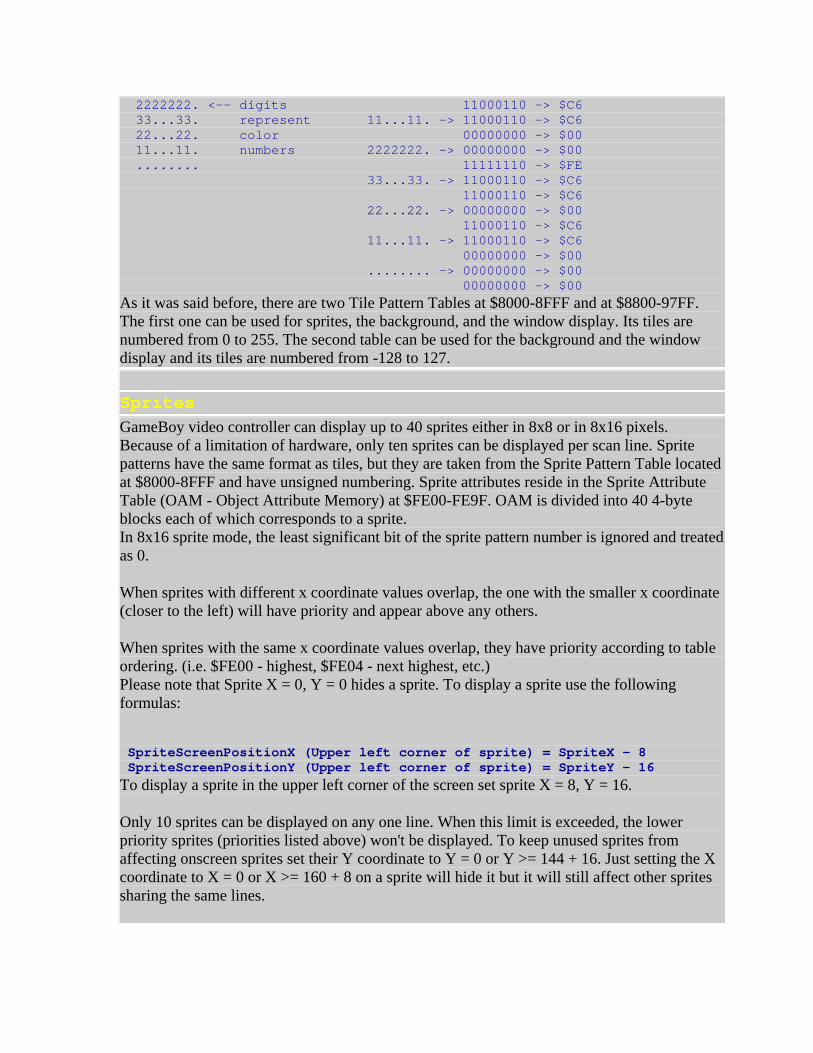
2222222. <-- digits 11000110 -> $C6 33...33. represent 11...11. -> 11000110 -> $C6 22...22. color 00000000 -> $00 11...11. numbers 2222222. -> 00000000 -> $00 ........ 11111110 -> $FE 33...33. -> 11000110 -> $C6 11000110 -> $C6 22...22. -> 00000000 -> $00 11000110 -> $C6 11...11. -> 11000110 -> $C6 00000000 -> $00 ........ -> 00000000 -> $00 00000000 -> $00 As it was said before, there are two Tile Pattern Tables at $8000-8FFF and at $8800-97FF. The first one can be used for sprites, the background, and the window display. Its tiles are numbered from 0 to 255. The second table can be used for the background and the window display and its tiles are numbered from -128 to 127. Sprites GameBoy video controller can display up to 40 sprites either in 8x8 or in 8x16 pixels. Because of a limitation of hardware, only ten sprites can be displayed per scan line. Sprite patterns have the same format as tiles, but they are taken from the Sprite Pattern Table located at $8000-8FFF and have unsigned numbering. Sprite attributes reside in the Sprite Attribute Table (OAM - Object Attribute Memory) at $FE00-FE9F. OAM is divided into 40 4-byte blocks each of which corresponds to a sprite. In 8x16 sprite mode, the least significant bit of the sprite pattern number is ignored and treated as 0.
When sprites with different x coordinate values overlap, the one with the smaller x coordinate (closer to the left) will have priority and appear above any others.
When sprites with the same x coordinate values overlap, they have priority according to table ordering. (i.e. $FE00 - highest, $FE04 - next highest, etc.) Please note that Sprite X = 0, Y = 0 hides a sprite. To display a sprite use the following formulas:
SpriteScreenPositionX (Upper left corner of sprite) = SpriteX - 8 SpriteScreenPositionY (Upper left corner of sprite) = SpriteY - 16 To display a sprite in the upper left corner of the screen set sprite X = 8, Y = 16.
Only 10 sprites can be displayed on any one line. When this limit is exceeded, the lower priority sprites (priorities listed above) won't be displayed. To keep unused sprites from affecting onscreen sprites set their Y coordinate to Y = 0 or Y >= 144 + 16. Just setting the X coordinate to X = 0 or X >= 160 + 8 on a sprite will hide it but it will still affect other sprites sharing the same lines.
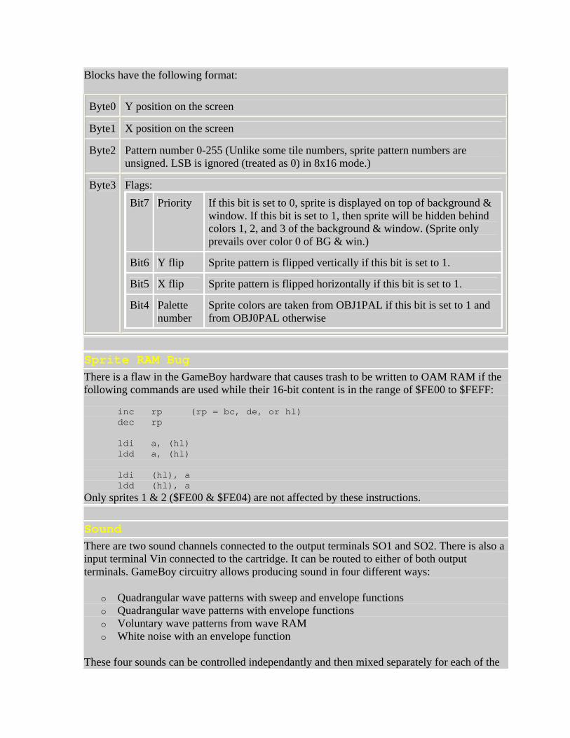
Blocks have the following format:
Byte0 Y position on the screen
Byte1 X position on the screen
Byte2 Pattern number 0-255 (Unlike some tile numbers, sprite pattern numbers are unsigned. LSB is ignored (treated as 0) in 8x16 mode.)
Byte3 Flags: Bit7 Priority If this bit is set to 0, sprite is displayed on top of background &
window. If this bit is set to 1, then sprite will be hidden behind colors 1, 2, and 3 of the background & window. (Sprite only prevails over color 0 of BG & win.)
Bit6 Y flip Sprite pattern is flipped vertically if this bit is set to 1.
Bit5 X flip Sprite pattern is flipped horizontally if this bit is set to 1.
Bit4 Palette number
Sprite colors are taken from OBJ1PAL if this bit is set to 1 and from OBJ0PAL otherwise
Sprite RAM Bug There is a flaw in the GameBoy hardware that causes trash to be written to OAM RAM if the following commands are used while their 16-bit content is in the range of $FE00 to $FEFF: inc rp (rp = bc, de, or hl) dec rp ldi a, (hl) ldd a, (hl) ldi (hl), a ldd (hl), a Only sprites 1 & 2 ($FE00 & $FE04) are not affected by these instructions. Sound There are two sound channels connected to the output terminals SO1 and SO2. There is also a input terminal Vin connected to the cartridge. It can be routed to either of both output terminals. GameBoy circuitry allows producing sound in four different ways:
o Quadrangular wave patterns with sweep and envelope functions o Quadrangular wave patterns with envelope functions o Voluntary wave patterns from wave RAM o White noise with an envelope function
These four sounds can be controlled independantly and then mixed separately for each of the
output terminals. Sound registers may be set at all times while producing sound. When setting the initial value of the envelope and restarting the length counter, set the initial flag to 1 and initialize the data.
Under the following situations the Sound ON flag is reset and the sound output stops:
1. When the sound output is stopped by the length counter 2. When overflow occurs at the addition mode while sweep is operating at sound 1.
When the Sound OFF flag for sound 3 (bit 7 of NR30) is set at 0, the cancellation of the OFF mode must be done by setting the sound OFF flag to 1. By initializing sound 3, it starts it's function. When the All Sound OFF flag (bit 7 of NR52) is set to 0, the mode registers for sounds 1, 2, 3, and 4 are reset and the sound output stops.
NOTE: The setting of each sounds mode register must be done after the All Sound OFF mode is cancelled. During the All Sound OFF mode, each sound mode register cannot be set.
NOTE: During the all sound off mode, GB power consumption drops by 16% or more! While your programs aren't using sound then set the all sound off flag to 0. It defaults to 1 on reset.
These tend to be the two most important equations in converting between Hertz and GB frequency registers: (Sounds will have a 2.4% higher frequency on Super GB.)
gb = 2048 - (131072 / Hz) Hz = 131072 / (2048 - gb)
Timer Sometimes it's useful to have a timer that interrupts at regular intervals for routines that require periodic or percise updates. The timer in the GameBoy has a selectable frequency of 4096, 16384, 65536, or 262144 Hertz. This frequency increments the Timer Counter (TIMA). When it overflows, it generates an interrupt. It is then loaded with the contents of Timer Modulo (TMA). The following are examples: ;This interval timer interrupts 4096 times per second ld a,-1 ld ($FF06),a ;Set TMA to divide clock by 1 ld a,4 ld ($FF07),a ;Set clock to 4096 Hertz ;This interval timer interrupts 65536 times per second ld a,-4 ld ($FF06),a ;Set TMA to divide clock by 4
ld a,5 ld ($FF07),a ;Set clock to 262144 Hertz
Serial I/O The serial I/O port on the Gameboy is a very simple setup and is crude compared to standard RS-232 (IBM-PC) or RS-485 (Macintosh) serial ports. There are no start or stop bits so the programmer must be more creative when using this port. During a transfer, a byte is shifted in at the same time that a byte is shifted out. The rate of the shift is deter- mined by whether the clock source is internal or external. If internal, the bits are shifted out at a rate of 8192Hz (122 microseconds) per bit. The most significant bit is shifted in and out first.
When the internal clock is selected, it drives the clock pin on the game link port and it stays high when not used. During a transfer it will go low eight times to clock in/out each bit.
A programmer initates a serial transfer by setting bit 7 of $FF02. This bit may be read and is automatically set to 0 at the completion of transfer. After this bit is set, an interrupt will then occur eight bit clocks later if the serial interrupt is enabled. If internal clock is selected and serial interrupt is enabled, this interrupt occurs 122*8 microseconds later. If external clock is selected and serial interrupt is enabled, an interrupt will occur eight bit clocks later.
Initiating a serial transfer with external clock will wait forever if no external clock is present. This allows a certain amount of synchronization with each serial port. The state of the last bit shifted out determines the state of the output line until another transfer takes place.
If a serial transfer with internal clock is performed and no external GameBoy is present, a value of $FF will be received in the transfer. The following code causes $75 to be shifted out the serial port and a byte to be shifted into $FF01:
ld a,$75 ld ($FF01),a ld a,$81 ld ($FF02),a
Interrupt Procedure The IME (interrupt master enable) flag is reset by DI and prohibits all interrupts. It is set by EI and acknowledges the interrupt setting by the IE register.
1. When an interrupt is generated, the IF flag will be set 2. If the IME flag is set & the corresponding IE flag is set, the following 3 steps are
performed 3. Reset the IME flag and prevent all interrupts 4. The PC (program counter) is pushed onto the stack

5. Jump to the starting address of the interrupt
Resetting of the IF register, which was the cause of the interrupt, is done by hardware.
During the interrupt, pushing of registers to be used should be performed by the interrupt routine. Once the interrupt service is in progress, all the interrupts will be prohibited. However, if the IME flag and the IE flag are controlled, a number of interrupt services can be made possible by nesting.
Return from an interrupt routine can be performed by either RETI or RET instruction. The RETI instruction enables interrupts after doing a return operation.
If a RET is used as the final instruction in an interrupt routine, interrupts will remain disabled unless a EI was used in the interrupt routine or is used at a later time. The interrupt will be acknowledged during opcode fetch period of each instruction. Interrupt Descriptions The following interrupts only occur if they have been enabled in the Interrupt Enable register ($FFFF) and if the interrupts have actually been enabled using the EI instruction. V-Blank The V-Blank interrupt occurs ~59.7 times a second on a regular GB and
~61.1 times a second on a Super GB (SGB). This interrupt occurs at the beginning of the V-Blank period. During this period video hardware is not using video ram so it may be freely accessed. This period lasts approximately 1.1 milliseconds.
LCDC Status
There are various reasons for this interrupt to occur as described by the STAT register ($FF40). One very popular reason is to indicate to the user when the video hardware is about to redraw a given LCD line. This can be useful for dynamically controlling the SCX / SCY registers ($FF43 / $FF42) to perform special video effects.
Timer Overflow
This interrupt occurs when the TIMA register ($FF05) changes from $FF to $00
Serial Transfer Completion
This interrupt occurs when a serial transfer has completed on the game link port.
High-to-Low of P10-P13
This interrupt occurs on a transition of any of the keypad input lines from high to low. Due to the fact that keypad "bounce"* is virtually always present, software should expect this interrupt to occur one or more times for every button press and one or more times for every button release.
Bounce tends to be a side effect of any button making or breaking a connection. During these periods, it is very common for a small amount of oscillation between high & low states to take
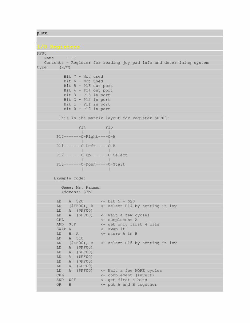
place. I/O Registers FF00 Name - P1 Contents - Register for reading joy pad info and determining system type. (R/W) Bit 7 - Not used Bit 6 - Not used Bit 5 - P15 out port Bit 4 - P14 out port Bit 3 - P13 in port Bit 2 - P12 in port Bit 1 - P11 in port Bit 0 - P10 in port This is the matrix layout for register $FF00: P14 P15 | | P10-------O-Right----O-A | | P11-------O-Left-----O-B | | P12-------O-Up-------O-Select | | P13-------O-Down-----O-Start | | Example code: Game: Ms. Pacman Address: $3b1 LD A, $20 <- bit 5 = $20 LD ($FF00), A <- select P14 by setting it low LD A, ($FF00) LD A, ($FF00) <- wait a few cycles CPL <- complement A AND $0F <- get only first 4 bits SWAP A <- swap it LD B, A <- store A in B LD A, $10 LD ($FF00), A <- select P15 by setting it low LD A, ($FF00) LD A, ($FF00) LD A, ($FF00) LD A, ($FF00) LD A, ($FF00) LD A, ($FF00) <- Wait a few MORE cycles CPL <- complement (invert) AND $0F <- get first 4 bits OR B <- put A and B together
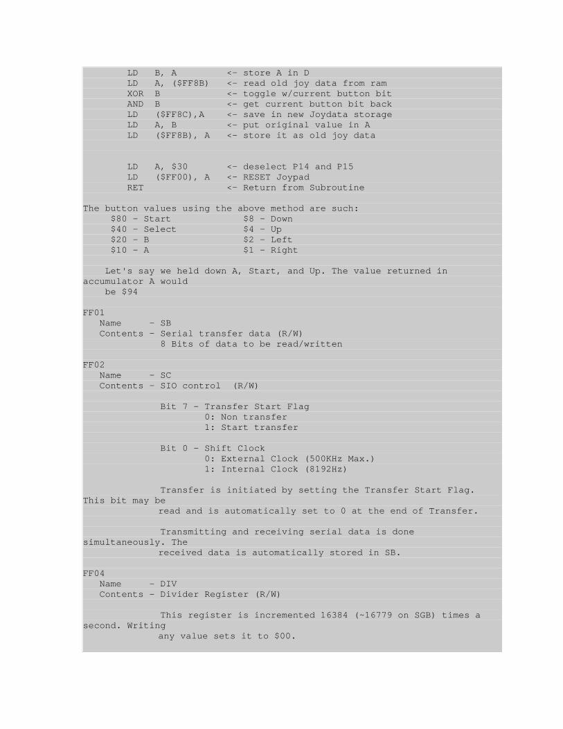
LD B, A <- store A in D LD A, ($FF8B) <- read old joy data from ram XOR B <- toggle w/current button bit AND B <- get current button bit back LD ($FF8C),A <- save in new Joydata storage LD A, B <- put original value in A LD ($FF8B), A <- store it as old joy data LD A, $30 <- deselect P14 and P15 LD ($FF00), A <- RESET Joypad RET <- Return from Subroutine The button values using the above method are such: $80 - Start $8 - Down $40 - Select $4 - Up $20 - B $2 - Left $10 - A $1 - Right Let's say we held down A, Start, and Up. The value returned in accumulator A would be $94 FF01 Name - SB Contents - Serial transfer data (R/W) 8 Bits of data to be read/written FF02 Name - SC Contents - SIO control (R/W) Bit 7 - Transfer Start Flag 0: Non transfer 1: Start transfer Bit 0 - Shift Clock 0: External Clock (500KHz Max.) 1: Internal Clock (8192Hz) Transfer is initiated by setting the Transfer Start Flag. This bit may be read and is automatically set to 0 at the end of Transfer. Transmitting and receiving serial data is done simultaneously. The received data is automatically stored in SB. FF04 Name - DIV Contents - Divider Register (R/W) This register is incremented 16384 (~16779 on SGB) times a second. Writing any value sets it to $00.
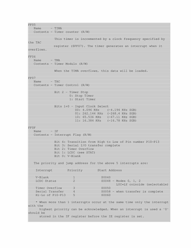
FF05 Name - TIMA Contents - Timer counter (R/W) This timer is incremented by a clock frequency specified by the TAC register ($FF07). The timer generates an interrupt when it overflows. FF06 Name - TMA Contents - Timer Modulo (R/W) When the TIMA overflows, this data will be loaded. FF07 Name - TAC Contents - Timer Control (R/W) Bit 2 - Timer Stop 0: Stop Timer 1: Start Timer Bits 1+0 - Input Clock Select 00: 4.096 KHz (~4.194 KHz SGB) 01: 262.144 KHz (~268.4 KHz SGB) 10: 65.536 KHz (~67.11 KHz SGB) 11: 16.384 KHz (~16.78 KHz SGB) FF0F Name - IF Contents - Interrupt Flag (R/W) Bit 4: Transition from High to Low of Pin number P10-P13 Bit 3: Serial I/O transfer complete Bit 2: Timer Overflow Bit 1: LCDC (see STAT) Bit 0: V-Blank The priority and jump address for the above 5 interrupts are: Interrupt Priority Start Address V-Blank 1 $0040 LCDC Status 2 $0048 - Modes 0, 1, 2 LYC=LY coincide (selectable) Timer Overflow 3 $0050 Serial Transfer 4 $0058 - when transfer is complete Hi-Lo of P10-P13 5 $0060 * When more than 1 interrupts occur at the same time only the interrupt with the highest priority can be acknowledged. When an interrupt is used a '0' should be stored in the IF register before the IE register is set.
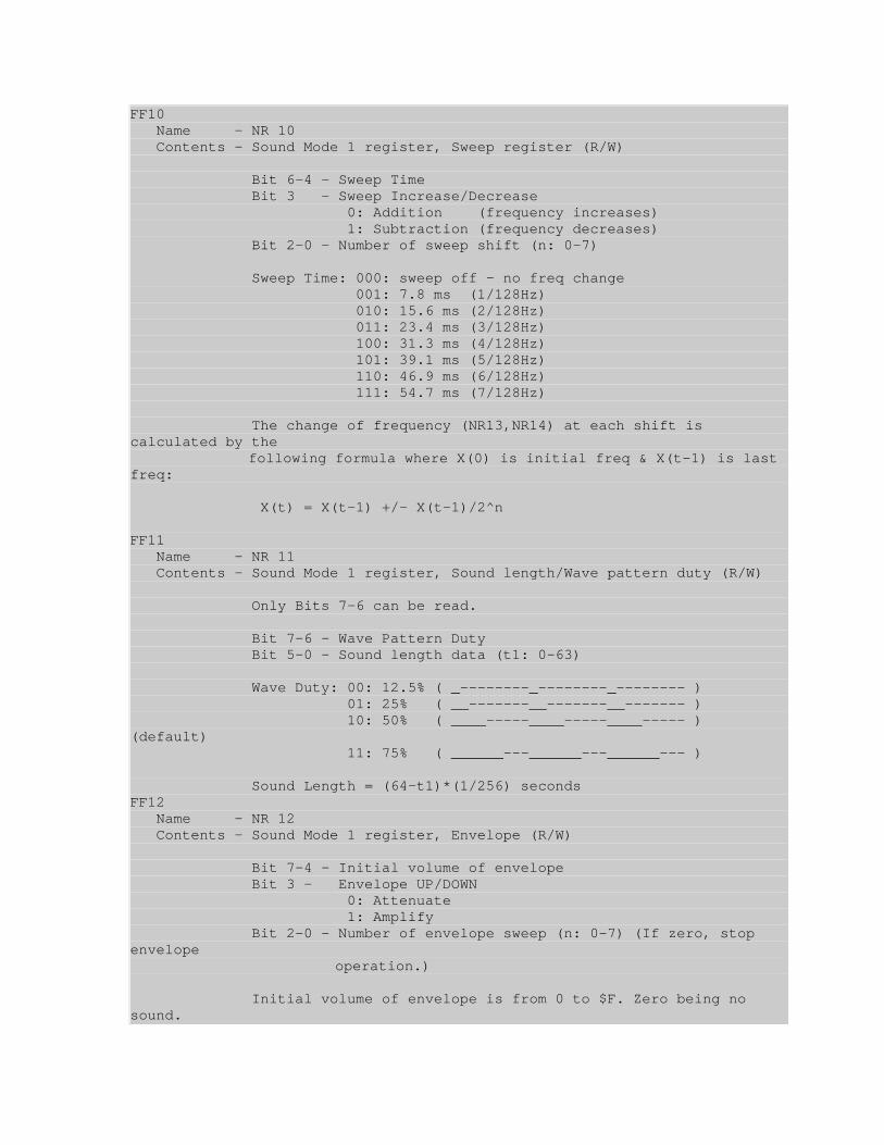
FF10 Name - NR 10 Contents - Sound Mode 1 register, Sweep register (R/W) Bit 6-4 - Sweep Time Bit 3 - Sweep Increase/Decrease 0: Addition (frequency increases) 1: Subtraction (frequency decreases) Bit 2-0 - Number of sweep shift (n: 0-7) Sweep Time: 000: sweep off - no freq change 001: 7.8 ms (1/128Hz) 010: 15.6 ms (2/128Hz) 011: 23.4 ms (3/128Hz) 100: 31.3 ms (4/128Hz) 101: 39.1 ms (5/128Hz) 110: 46.9 ms (6/128Hz) 111: 54.7 ms (7/128Hz) The change of frequency (NR13,NR14) at each shift is calculated by the following formula where X(0) is initial freq & X(t-1) is last freq: X(t) = X(t-1) +/- X(t-1)/2^n FF11 Name - NR 11 Contents - Sound Mode 1 register, Sound length/Wave pattern duty (R/W) Only Bits 7-6 can be read. Bit 7-6 - Wave Pattern Duty Bit 5-0 - Sound length data (t1: 0-63) Wave Duty: 00: 12.5% ( _--------_--------_-------- ) 01: 25% ( __-------__-------__------- ) 10: 50% ( ____-----____-----____----- ) (default) 11: 75% ( ______---______---______--- ) Sound Length = (64-t1)*(1/256) seconds FF12 Name - NR 12 Contents - Sound Mode 1 register, Envelope (R/W) Bit 7-4 - Initial volume of envelope Bit 3 - Envelope UP/DOWN 0: Attenuate 1: Amplify Bit 2-0 - Number of envelope sweep (n: 0-7) (If zero, stop envelope operation.) Initial volume of envelope is from 0 to $F. Zero being no sound.
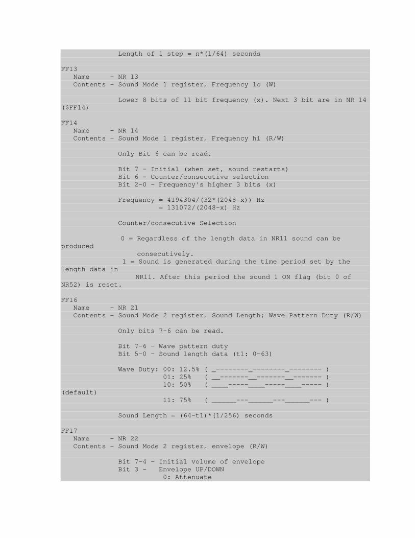
Length of 1 step = n*(1/64) seconds FF13 Name - NR 13 Contents - Sound Mode 1 register, Frequency lo (W) Lower 8 bits of 11 bit frequency (x). Next 3 bit are in NR 14 ($FF14) FF14 Name - NR 14 Contents - Sound Mode 1 register, Frequency hi (R/W) Only Bit 6 can be read. Bit 7 - Initial (when set, sound restarts) Bit 6 - Counter/consecutive selection Bit 2-0 - Frequency's higher 3 bits (x) Frequency = 4194304/(32*(2048-x)) Hz = 131072/(2048-x) Hz Counter/consecutive Selection 0 = Regardless of the length data in NR11 sound can be produced consecutively. 1 = Sound is generated during the time period set by the length data in NR11. After this period the sound 1 ON flag (bit 0 of NR52) is reset. FF16 Name - NR 21 Contents - Sound Mode 2 register, Sound Length; Wave Pattern Duty (R/W) Only bits 7-6 can be read. Bit 7-6 - Wave pattern duty Bit 5-0 - Sound length data (t1: 0-63) Wave Duty: 00: 12.5% ( _--------_--------_-------- ) 01: 25% ( __-------__-------__------- ) 10: 50% ( ____-----____-----____----- ) (default) 11: 75% ( ______---______---______--- ) Sound Length = (64-t1)*(1/256) seconds FF17 Name - NR 22 Contents - Sound Mode 2 register, envelope (R/W) Bit 7-4 - Initial volume of envelope Bit 3 - Envelope UP/DOWN 0: Attenuate
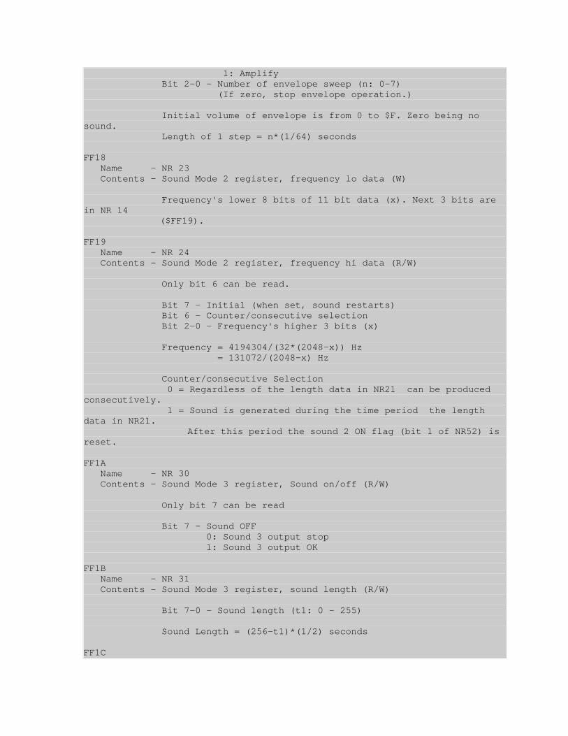
1: Amplify Bit 2-0 - Number of envelope sweep (n: 0-7) (If zero, stop envelope operation.) Initial volume of envelope is from 0 to $F. Zero being no sound. Length of 1 step = n*(1/64) seconds FF18 Name - NR 23 Contents - Sound Mode 2 register, frequency lo data (W) Frequency's lower 8 bits of 11 bit data (x). Next 3 bits are in NR 14 ($FF19). FF19 Name - NR 24 Contents - Sound Mode 2 register, frequency hi data (R/W) Only bit 6 can be read. Bit 7 - Initial (when set, sound restarts) Bit 6 - Counter/consecutive selection Bit 2-0 - Frequency's higher 3 bits (x) Frequency = 4194304/(32*(2048-x)) Hz = 131072/(2048-x) Hz Counter/consecutive Selection 0 = Regardless of the length data in NR21 can be produced consecutively. 1 = Sound is generated during the time period the length data in NR21. After this period the sound 2 ON flag (bit 1 of NR52) is reset. FF1A Name - NR 30 Contents - Sound Mode 3 register, Sound on/off (R/W) Only bit 7 can be read Bit 7 - Sound OFF 0: Sound 3 output stop 1: Sound 3 output OK FF1B Name - NR 31 Contents - Sound Mode 3 register, sound length (R/W) Bit 7-0 - Sound length (t1: 0 - 255) Sound Length = (256-t1)*(1/2) seconds FF1C
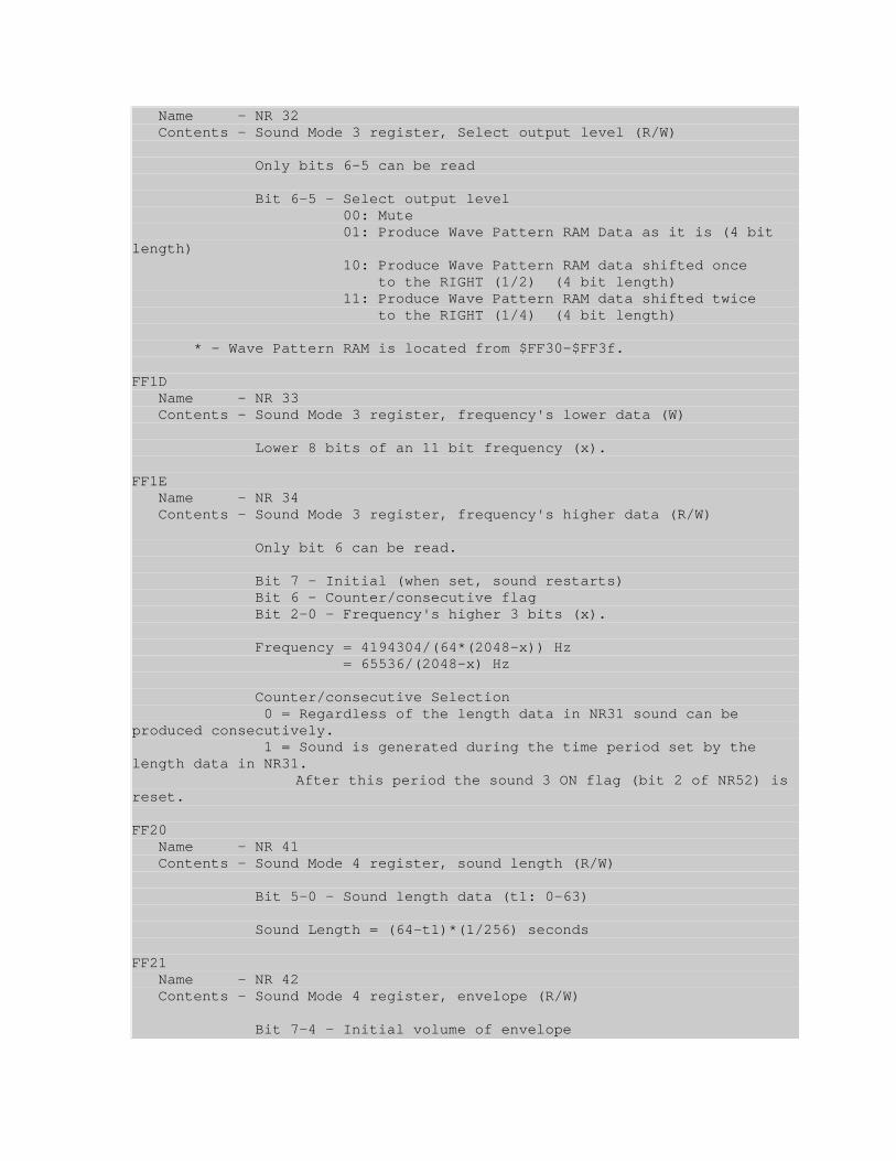
Name - NR 32 Contents - Sound Mode 3 register, Select output level (R/W) Only bits 6-5 can be read Bit 6-5 - Select output level 00: Mute 01: Produce Wave Pattern RAM Data as it is (4 bit length) 10: Produce Wave Pattern RAM data shifted once to the RIGHT (1/2) (4 bit length) 11: Produce Wave Pattern RAM data shifted twice to the RIGHT (1/4) (4 bit length) * - Wave Pattern RAM is located from $FF30-$FF3f. FF1D Name - NR 33 Contents - Sound Mode 3 register, frequency's lower data (W) Lower 8 bits of an 11 bit frequency (x). FF1E Name - NR 34 Contents - Sound Mode 3 register, frequency's higher data (R/W) Only bit 6 can be read. Bit 7 - Initial (when set, sound restarts) Bit 6 - Counter/consecutive flag Bit 2-0 - Frequency's higher 3 bits (x). Frequency = 4194304/(64*(2048-x)) Hz = 65536/(2048-x) Hz Counter/consecutive Selection 0 = Regardless of the length data in NR31 sound can be produced consecutively. 1 = Sound is generated during the time period set by the length data in NR31. After this period the sound 3 ON flag (bit 2 of NR52) is reset. FF20 Name - NR 41 Contents - Sound Mode 4 register, sound length (R/W) Bit 5-0 - Sound length data (t1: 0-63) Sound Length = (64-t1)*(1/256) seconds FF21 Name - NR 42 Contents - Sound Mode 4 register, envelope (R/W) Bit 7-4 - Initial volume of envelope
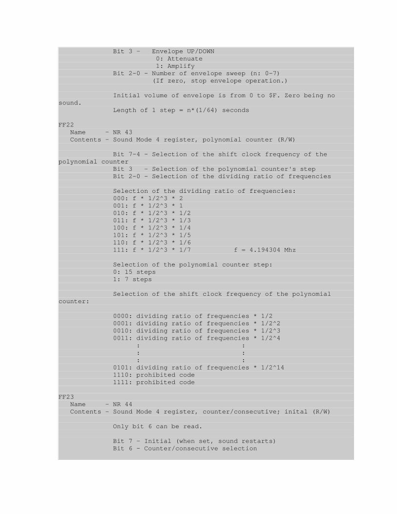
Bit 3 - Envelope UP/DOWN 0: Attenuate 1: Amplify Bit 2-0 - Number of envelope sweep (n: 0-7) (If zero, stop envelope operation.) Initial volume of envelope is from 0 to $F. Zero being no sound. Length of 1 step = n*(1/64) seconds FF22 Name - NR 43 Contents - Sound Mode 4 register, polynomial counter (R/W) Bit 7-4 - Selection of the shift clock frequency of the polynomial counter Bit 3 - Selection of the polynomial counter's step Bit 2-0 - Selection of the dividing ratio of frequencies Selection of the dividing ratio of frequencies: 000: f * 1/2^3 * 2 001: f * 1/2^3 * 1 010: f * 1/2^3 * 1/2 011: f * 1/2^3 * 1/3 100: f * 1/2^3 * 1/4 101: f * 1/2^3 * 1/5 110: f * 1/2^3 * 1/6 111: f * 1/2^3 * 1/7 f = 4.194304 Mhz Selection of the polynomial counter step: 0: 15 steps 1: 7 steps Selection of the shift clock frequency of the polynomial counter: 0000: dividing ratio of frequencies * 1/2 0001: dividing ratio of frequencies * 1/2^2 0010: dividing ratio of frequencies * 1/2^3 0011: dividing ratio of frequencies * 1/2^4 : : : : : : 0101: dividing ratio of frequencies * 1/2^14 1110: prohibited code 1111: prohibited code FF23 Name - NR 44 Contents - Sound Mode 4 register, counter/consecutive; inital (R/W) Only bit 6 can be read. Bit 7 - Initial (when set, sound restarts) Bit 6 - Counter/consecutive selection
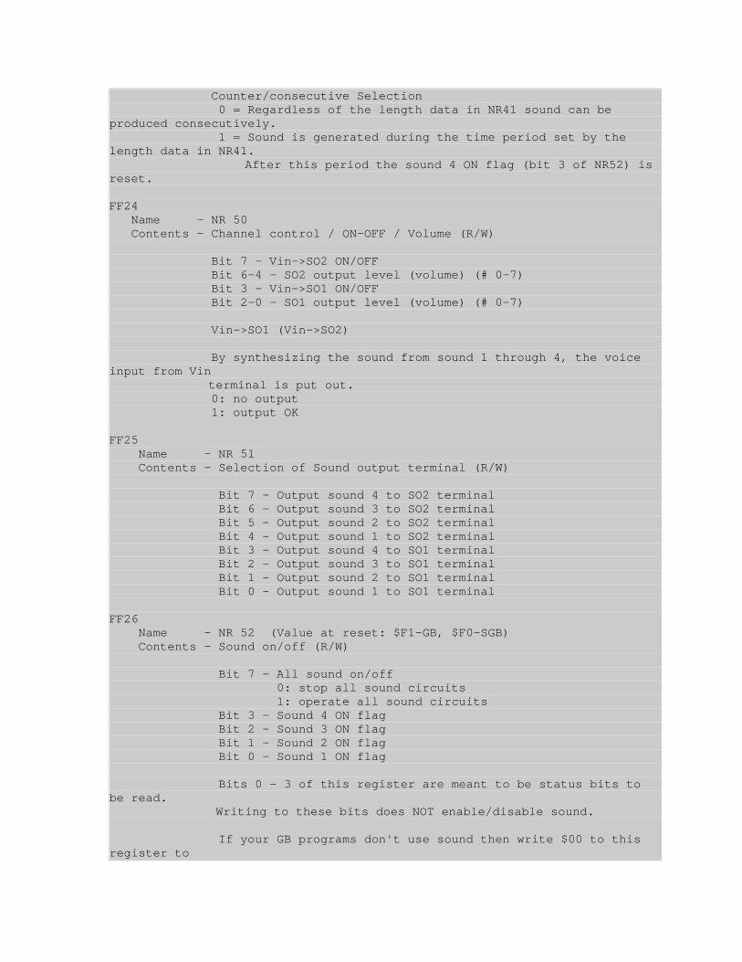
Counter/consecutive Selection 0 = Regardless of the length data in NR41 sound can be produced consecutively. 1 = Sound is generated during the time period set by the length data in NR41. After this period the sound 4 ON flag (bit 3 of NR52) is reset. FF24 Name - NR 50 Contents - Channel control / ON-OFF / Volume (R/W) Bit 7 - Vin->SO2 ON/OFF Bit 6-4 - SO2 output level (volume) (# 0-7) Bit 3 - Vin->SO1 ON/OFF Bit 2-0 - SO1 output level (volume) (# 0-7) Vin->SO1 (Vin->SO2) By synthesizing the sound from sound 1 through 4, the voice input from Vin terminal is put out. 0: no output 1: output OK FF25 Name - NR 51 Contents - Selection of Sound output terminal (R/W) Bit 7 - Output sound 4 to SO2 terminal Bit 6 - Output sound 3 to SO2 terminal Bit 5 - Output sound 2 to SO2 terminal Bit 4 - Output sound 1 to SO2 terminal Bit 3 - Output sound 4 to SO1 terminal Bit 2 - Output sound 3 to SO1 terminal Bit 1 - Output sound 2 to SO1 terminal Bit 0 - Output sound 1 to SO1 terminal FF26 Name - NR 52 (Value at reset: $F1-GB, $F0-SGB) Contents - Sound on/off (R/W) Bit 7 - All sound on/off 0: stop all sound circuits 1: operate all sound circuits Bit 3 - Sound 4 ON flag Bit 2 - Sound 3 ON flag Bit 1 - Sound 2 ON flag Bit 0 - Sound 1 ON flag Bits 0 - 3 of this register are meant to be status bits to be read. Writing to these bits does NOT enable/disable sound. If your GB programs don't use sound then write $00 to this register to
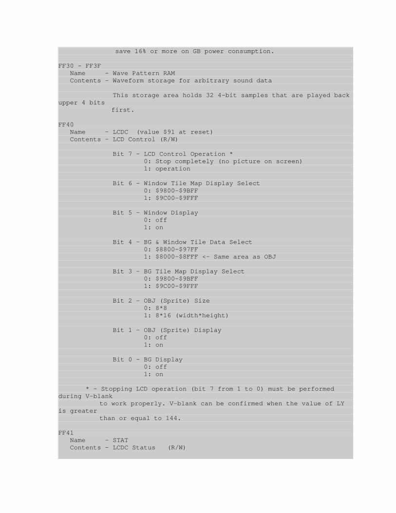
save 16% or more on GB power consumption. FF30 - FF3F Name - Wave Pattern RAM Contents - Waveform storage for arbitrary sound data This storage area holds 32 4-bit samples that are played back upper 4 bits first. FF40 Name - LCDC (value $91 at reset) Contents - LCD Control (R/W) Bit 7 - LCD Control Operation * 0: Stop completely (no picture on screen) 1: operation Bit 6 - Window Tile Map Display Select 0: $9800-$9BFF 1: $9C00-$9FFF Bit 5 - Window Display 0: off 1: on Bit 4 - BG & Window Tile Data Select 0: $8800-$97FF 1: $8000-$8FFF <- Same area as OBJ Bit 3 - BG Tile Map Display Select 0: $9800-$9BFF 1: $9C00-$9FFF Bit 2 - OBJ (Sprite) Size 0: 8*8 1: 8*16 (width*height) Bit 1 - OBJ (Sprite) Display 0: off 1: on Bit 0 - BG Display 0: off 1: on * - Stopping LCD operation (bit 7 from 1 to 0) must be performed during V-blank to work properly. V-blank can be confirmed when the value of LY is greater than or equal to 144. FF41 Name - STAT Contents - LCDC Status (R/W)
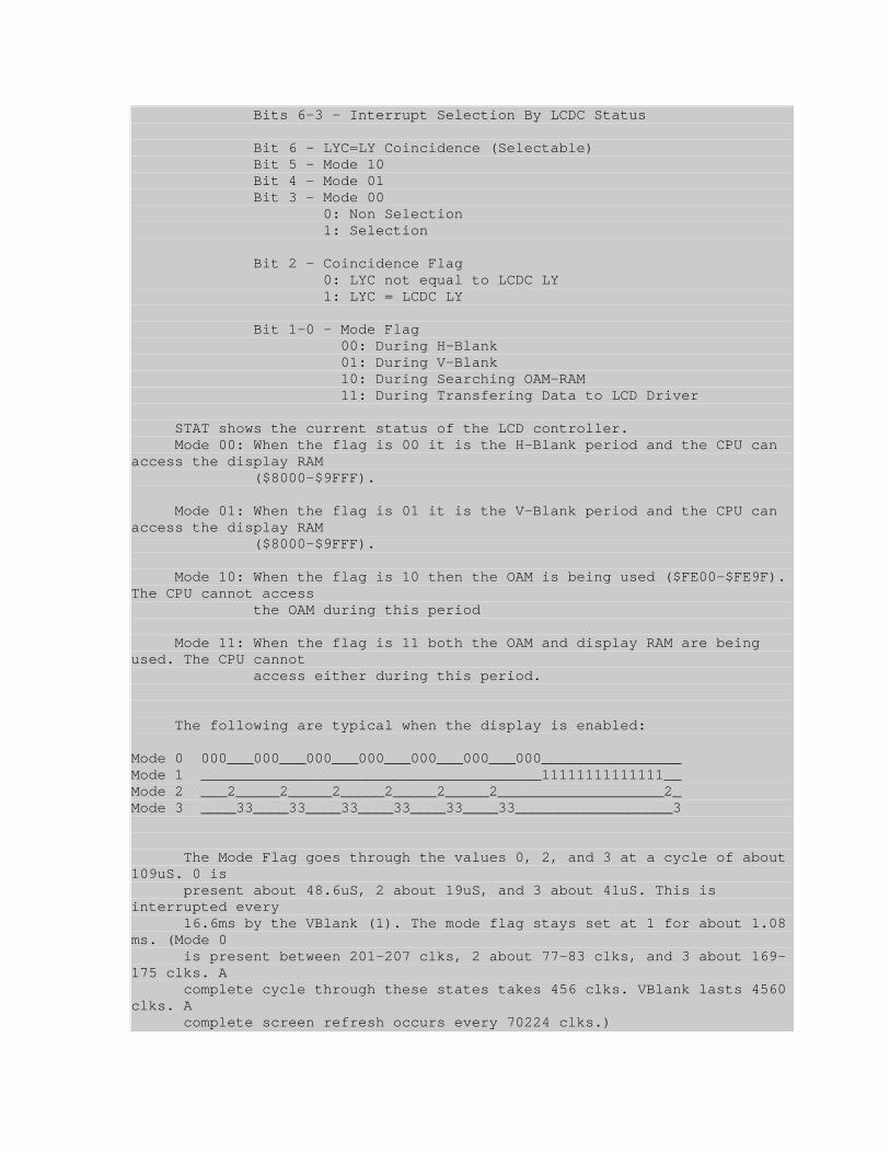
Bits 6-3 - Interrupt Selection By LCDC Status Bit 6 - LYC=LY Coincidence (Selectable) Bit 5 - Mode 10 Bit 4 - Mode 01 Bit 3 - Mode 00 0: Non Selection 1: Selection Bit 2 - Coincidence Flag 0: LYC not equal to LCDC LY 1: LYC = LCDC LY Bit 1-0 - Mode Flag 00: During H-Blank 01: During V-Blank 10: During Searching OAM-RAM 11: During Transfering Data to LCD Driver STAT shows the current status of the LCD controller. Mode 00: When the flag is 00 it is the H-Blank period and the CPU can access the display RAM ($8000-$9FFF). Mode 01: When the flag is 01 it is the V-Blank period and the CPU can access the display RAM ($8000-$9FFF). Mode 10: When the flag is 10 then the OAM is being used ($FE00-$FE9F). The CPU cannot access the OAM during this period Mode 11: When the flag is 11 both the OAM and display RAM are being used. The CPU cannot access either during this period. The following are typical when the display is enabled: Mode 0 000___000___000___000___000___000___000________________ Mode 1 _______________________________________11111111111111__ Mode 2 ___2_____2_____2_____2_____2_____2___________________2_ Mode 3 ____33____33____33____33____33____33__________________3 The Mode Flag goes through the values 0, 2, and 3 at a cycle of about 109uS. 0 is present about 48.6uS, 2 about 19uS, and 3 about 41uS. This is interrupted every 16.6ms by the VBlank (1). The mode flag stays set at 1 for about 1.08 ms. (Mode 0 is present between 201-207 clks, 2 about 77-83 clks, and 3 about 169-175 clks. A complete cycle through these states takes 456 clks. VBlank lasts 4560 clks. A complete screen refresh occurs every 70224 clks.)
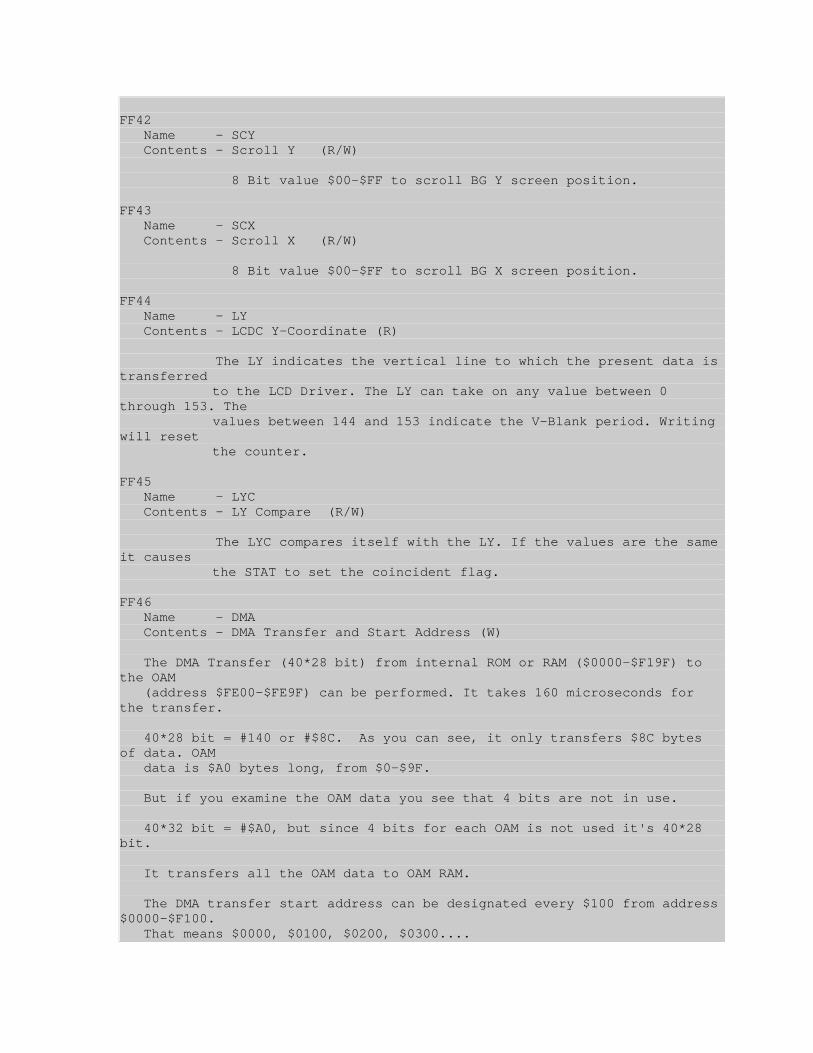
FF42 Name - SCY Contents - Scroll Y (R/W) 8 Bit value $00-$FF to scroll BG Y screen position. FF43 Name - SCX Contents - Scroll X (R/W) 8 Bit value $00-$FF to scroll BG X screen position. FF44 Name - LY Contents - LCDC Y-Coordinate (R) The LY indicates the vertical line to which the present data is transferred to the LCD Driver. The LY can take on any value between 0 through 153. The values between 144 and 153 indicate the V-Blank period. Writing will reset the counter. FF45 Name - LYC Contents - LY Compare (R/W) The LYC compares itself with the LY. If the values are the same it causes the STAT to set the coincident flag. FF46 Name - DMA Contents - DMA Transfer and Start Address (W) The DMA Transfer (40*28 bit) from internal ROM or RAM ($0000-$F19F) to the OAM (address $FE00-$FE9F) can be performed. It takes 160 microseconds for the transfer. 40*28 bit = #140 or #$8C. As you can see, it only transfers $8C bytes of data. OAM data is $A0 bytes long, from $0-$9F. But if you examine the OAM data you see that 4 bits are not in use. 40*32 bit = #$A0, but since 4 bits for each OAM is not used it's 40*28 bit. It transfers all the OAM data to OAM RAM. The DMA transfer start address can be designated every $100 from address $0000-$F100. That means $0000, $0100, $0200, $0300....
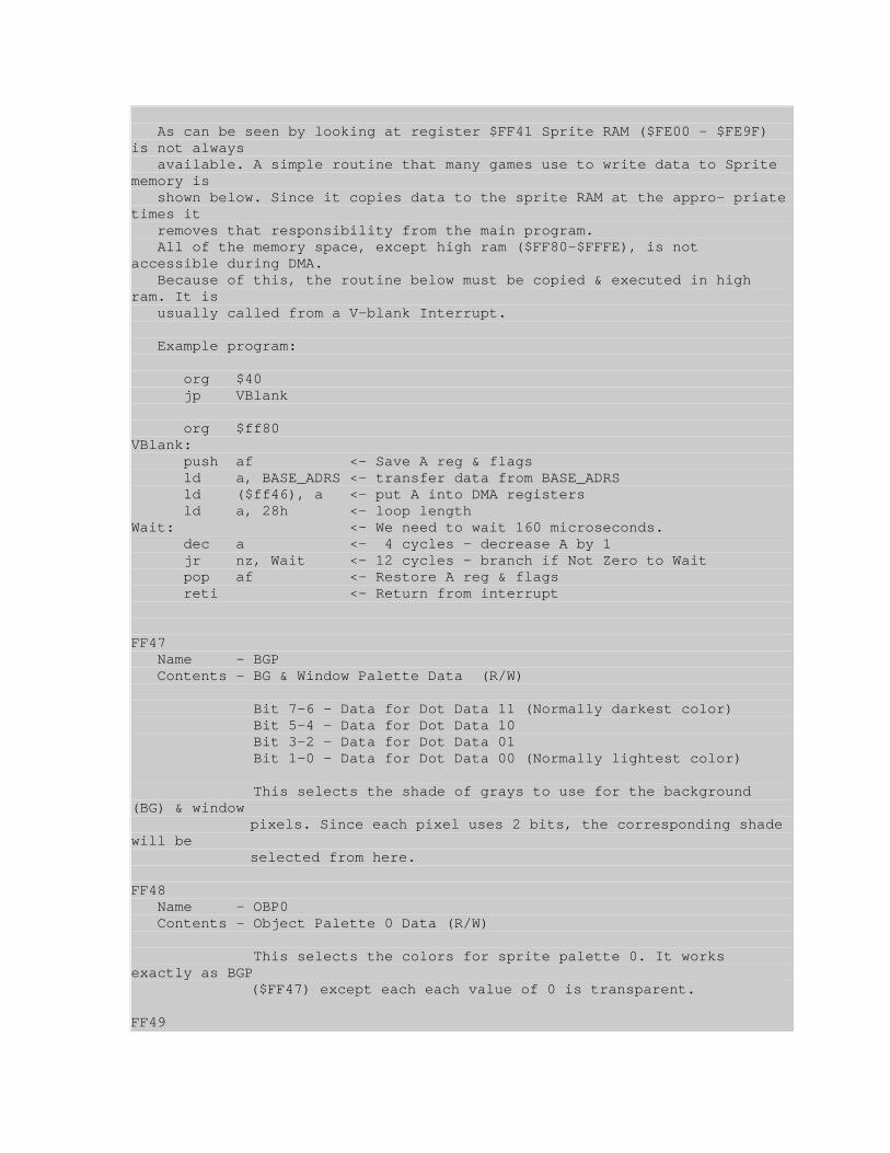
As can be seen by looking at register $FF41 Sprite RAM ($FE00 - $FE9F) is not always available. A simple routine that many games use to write data to Sprite memory is shown below. Since it copies data to the sprite RAM at the appro- priate times it removes that responsibility from the main program. All of the memory space, except high ram ($FF80-$FFFE), is not accessible during DMA. Because of this, the routine below must be copied & executed in high ram. It is usually called from a V-blank Interrupt. Example program: org $40 jp VBlank org $ff80 VBlank: push af <- Save A reg & flags ld a, BASE_ADRS <- transfer data from BASE_ADRS ld ($ff46), a <- put A into DMA registers ld a, 28h <- loop length Wait: <- We need to wait 160 microseconds. dec a <- 4 cycles - decrease A by 1 jr nz, Wait <- 12 cycles - branch if Not Zero to Wait pop af <- Restore A reg & flags reti <- Return from interrupt FF47 Name - BGP Contents - BG & Window Palette Data (R/W) Bit 7-6 - Data for Dot Data 11 (Normally darkest color) Bit 5-4 - Data for Dot Data 10 Bit 3-2 - Data for Dot Data 01 Bit 1-0 - Data for Dot Data 00 (Normally lightest color) This selects the shade of grays to use for the background (BG) & window pixels. Since each pixel uses 2 bits, the corresponding shade will be selected from here. FF48 Name - OBP0 Contents - Object Palette 0 Data (R/W) This selects the colors for sprite palette 0. It works exactly as BGP ($FF47) except each each value of 0 is transparent. FF49
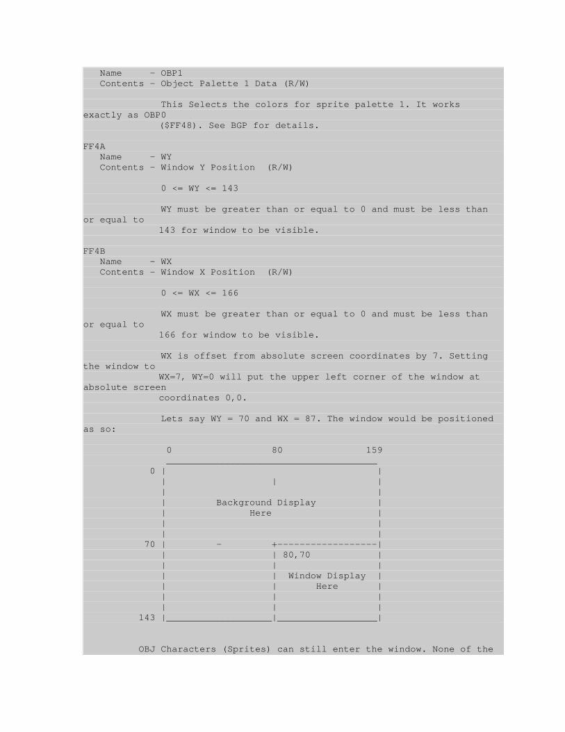
Name - OBP1 Contents - Object Palette 1 Data (R/W) This Selects the colors for sprite palette 1. It works exactly as OBP0 ($FF48). See BGP for details. FF4A Name - WY Contents - Window Y Position (R/W) 0 <= WY <= 143 WY must be greater than or equal to 0 and must be less than or equal to 143 for window to be visible. FF4B Name - WX Contents - Window X Position (R/W) 0 <= WX <= 166 WX must be greater than or equal to 0 and must be less than or equal to 166 for window to be visible. WX is offset from absolute screen coordinates by 7. Setting the window to WX=7, WY=0 will put the upper left corner of the window at absolute screen coordinates 0,0. Lets say WY = 70 and WX = 87. The window would be positioned as so: 0 80 159 ______________________________________ 0 | | | | | | | | Background Display | | Here | | | | | 70 | - +------------------| | | 80,70 | | | | | | Window Display | | | Here | | | | | | | 143 |___________________|__________________| OBJ Characters (Sprites) can still enter the window. None of the
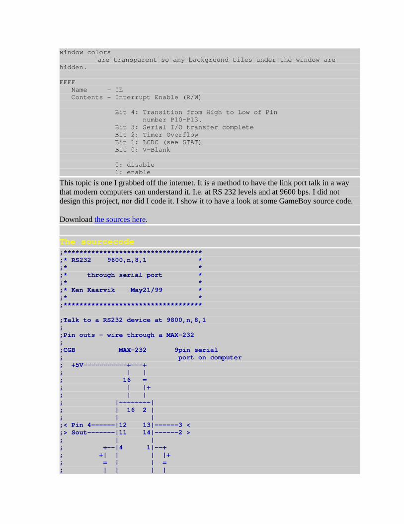
window colors are transparent so any background tiles under the window are hidden. FFFF Name - IE Contents - Interrupt Enable (R/W) Bit 4: Transition from High to Low of Pin number P10-P13. Bit 3: Serial I/O transfer complete Bit 2: Timer Overflow Bit 1: LCDC (see STAT) Bit 0: V-Blank 0: disable 1: enable
This topic is one I grabbed off the internet. It is a method to have the link port talk in a way that modern computers can understand it. I.e. at RS 232 levels and at 9600 bps. I did not design this project, nor did I code it. I show it to have a look at some GameBoy source code.
Download the sources here. The sourcecode ;*********************************** ;* RS232 9600,n,8,1 * ;* * ;* through serial port * ;* * ;* Ken Kaarvik May21/99 * ;* * ;*********************************** ;Talk to a RS232 device at 9800,n,8,1 ; ;Pin outs - wire through a MAX-232 ; ;CGB MAX-232 9pin serial ; port on computer ; +5V-----------+---+ ; | | ; 16 = ; | |+ ; | | ; |~~~~~~~~| ; | 16 2 | ; | | ;< Pin 4------|12 13|------3 < ;> Sout-------|11 14|------2 > ; | | ; +--|4 1|--+ ; +| | | |+ ; = | | = ; | | | |

; +--|5 3|--+ ; | | ; |__15__6_| ; | | ; | = ; | |+ ; gnd-----------+---+--------5 ; ; (4) caps @10uF Note polarity ; display_col equ $9800 blank equ 16 text_line equ $9800+$20*5 SECTION "Org $0", HOME ret ; Button Push Interrupt - For sending out data while waiting for input SECTION "Org $60",HOME[$60] push af call pad_Read call send_test xor a ldh [$00],a pop af reti INCLUDE "hardware.inc" INCLUDE "ibmpc1.inc" SECTION "Header",HOME[$0100] nop jp Startup DB $CE,$ED,$66,$66,$CC,$0D,$00,$0B,$03,$73,$00,$83,$00,$0C,$00,$0D DB $00,$08,$11,$1F,$88,$89,$00,$0E,$DC,$CC,$6E,$E6,$DD,$DD,$D9,$99 DB $BB,$BB,$67,$63,$6E,$0E,$EC,$CC,$DD,$DC,$99,$9F,$BB,$B9,$33,$3E ;0123456789ABCDE DB "RS232 " DB $80 ; $80=Color GB DB 0,0,0 ; SuperGameboy DB 0 ; CARTTYPE ; -------- ; 0 - ROM ONLY ; 1 - ROM+MBC1 ; 2 - ROM+MBC1+RAM ; 3 - ROM+MBC1+RAM+BATTERY
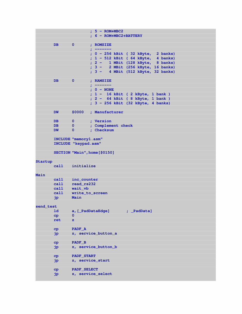
; 5 - ROM+MBC2 ; 6 - ROM+MBC2+BATTERY DB 0 ; ROMSIZE ; ------- ; 0 - 256 kBit ( 32 kByte, 2 banks) ; 1 - 512 kBit ( 64 kByte, 4 banks) ; 2 - 1 MBit (128 kByte, 8 banks) ; 3 - 2 MBit (256 kByte, 16 banks) ; 3 - 4 MBit (512 kByte, 32 banks) DB 0 ; RAMSIZE ; ------- ; 0 - NONE ; 1 - 16 kBit ( 2 kByte, 1 bank ) ; 2 - 64 kBit ( 8 kByte, 1 bank ) ; 3 - 256 kBit (32 kByte, 4 banks) DW $0000 ; Manufacturer DB 0 ; Version DB 0 ; Complement check DW 0 ; Checksum INCLUDE "memory1.asm" INCLUDE "keypad.asm" SECTION "Main",home[$0150] Startup call initialize Main call inc_counter call read_rs232 call wait_vb call write_to_screen jp Main send_test ld a,[_PadDataEdge] ; _PadData] cp 0 ret z cp PADF_A jp z, service_button_a cp PADF_B jp z, service_button_b cp PADF_START jp z, service_start cp PADF_SELECT jp z, service_select
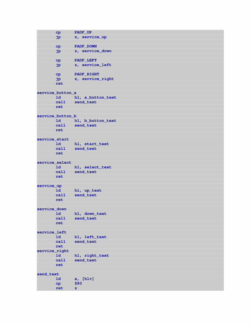
cp PADF_UP jp z, service_up cp PADF_DOWN jp z, service_down cp PADF_LEFT jp z, service_left cp PADF_RIGHT jp z, service_right ret service_button_a ld hl, a_button_text call send_text ret service_button_b ld hl, b_button_text call send_text ret service_start ld hl, start_text call send_text ret service_select ld hl, select_text call send_text ret service_up ld hl, up_text call send_text ret service_down ld hl, down_text call send_text ret service_left ld hl, left_text call send_text ret service_right ld hl, right_text call send_text ret send_text ld a, [hl+] cp $80 ret z
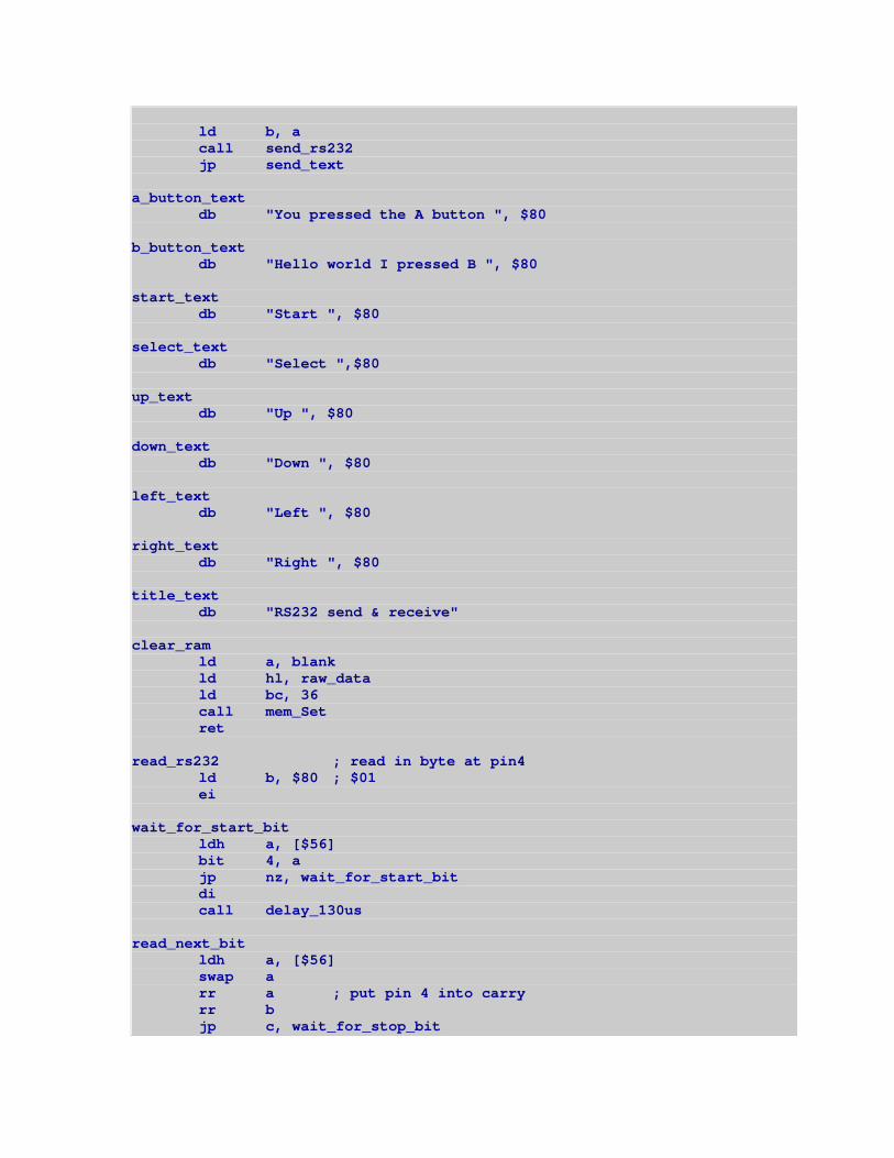
ld b, a call send_rs232 jp send_text a_button_text db "You pressed the A button ", $80 b_button_text db "Hello world I pressed B ", $80 start_text db "Start ", $80 select_text db "Select ",$80 up_text db "Up ", $80 down_text db "Down ", $80 left_text db "Left ", $80 right_text db "Right ", $80 title_text db "RS232 send & receive" clear_ram ld a, blank ld hl, raw_data ld bc, 36 call mem_Set ret read_rs232 ; read in byte at pin4 ld b, $80 ; $01 ei wait_for_start_bit ldh a, [$56] bit 4, a jp nz, wait_for_start_bit di call delay_130us read_next_bit ldh a, [$56] swap a rr a ; put pin 4 into carry rr b jp c, wait_for_stop_bit
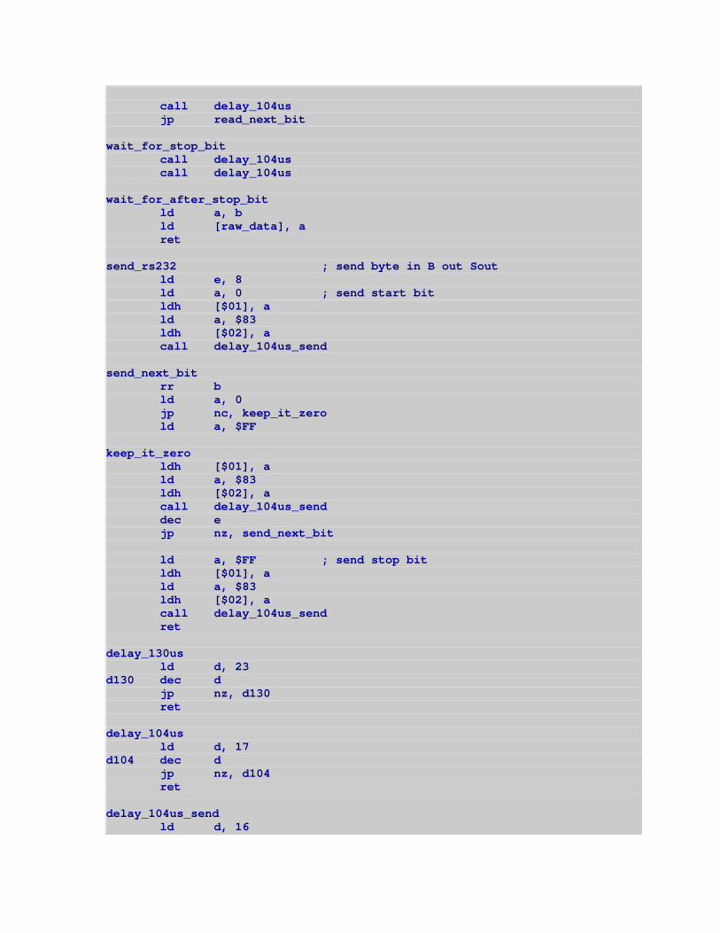
call delay_104us jp read_next_bit wait_for_stop_bit call delay_104us call delay_104us wait_for_after_stop_bit ld a, b ld [raw_data], a ret send_rs232 ; send byte in B out Sout ld e, 8 ld a, 0 ; send start bit ldh [$01], a ld a, $83 ldh [$02], a call delay_104us_send send_next_bit rr b ld a, 0 jp nc, keep_it_zero ld a, $FF keep_it_zero ldh [$01], a ld a, $83 ldh [$02], a call delay_104us_send dec e jp nz, send_next_bit ld a, $FF ; send stop bit ldh [$01], a ld a, $83 ldh [$02], a call delay_104us_send ret delay_130us ld d, 23 d130 dec d jp nz, d130 ret delay_104us ld d, 17 d104 dec d jp nz, d104 ret delay_104us_send ld d, 16

d104s dec d jp nz, d104s ret inc_counter ld a, [counter] inc a ld [counter], a ret write_to_screen call shift_display_left ld a, [raw_data] ld hl, text_line+19 call display_char ld de, counter ld hl, display_col+$20*3 call display_byte ret shift_display_left ld hl, text_line+1 ld de, text_line ld bc, 1 call mem_CopyVRAM ld hl, text_line+2 ld de, text_line+1 ld bc, 1 call mem_CopyVRAM ld hl, text_line+3 ld de, text_line+2 ld bc, 1 call mem_CopyVRAM ld hl, text_line+4 ld de, text_line+3 ld bc, 1 call mem_CopyVRAM ld hl, text_line+5 ld de, text_line+4 ld bc, 1 call mem_CopyVRAM ld hl, text_line+6 ld de, text_line+5 ld bc, 1 call mem_CopyVRAM ld hl, text_line+7 ld de, text_line+6 ld bc, 1 call mem_CopyVRAM
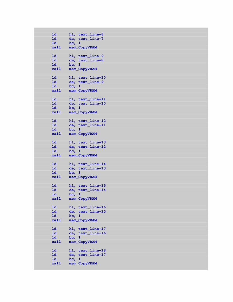
ld hl, text_line+8 ld de, text_line+7 ld bc, 1 call mem_CopyVRAM ld hl, text_line+9 ld de, text_line+8 ld bc, 1 call mem_CopyVRAM ld hl, text_line+10 ld de, text_line+9 ld bc, 1 call mem_CopyVRAM ld hl, text_line+11 ld de, text_line+10 ld bc, 1 call mem_CopyVRAM ld hl, text_line+12 ld de, text_line+11 ld bc, 1 call mem_CopyVRAM ld hl, text_line+13 ld de, text_line+12 ld bc, 1 call mem_CopyVRAM ld hl, text_line+14 ld de, text_line+13 ld bc, 1 call mem_CopyVRAM ld hl, text_line+15 ld de, text_line+14 ld bc, 1 call mem_CopyVRAM ld hl, text_line+16 ld de, text_line+15 ld bc, 1 call mem_CopyVRAM ld hl, text_line+17 ld de, text_line+16 ld bc, 1 call mem_CopyVRAM ld hl, text_line+18 ld de, text_line+17 ld bc, 1 call mem_CopyVRAM

ld hl, text_line+19 ld de, text_line+18 ld bc, 1 call mem_CopyVRAM ret display_byte ; enter with value in [de] lcd_WaitVRAM ld a, [de] ld b, a and $F0 swap a ld [hl+], a lcd_WaitVRAM ld a, b and $0F ld [hl], a ret display_char bit 7, a ;don't look up non print chars ret nz add a, 20 ;add imb char offset push af lcd_WaitVRAM pop af ld [hl], a ret initialize di .wait ldh a, [$44] ; LY LCDC compare cp 144 jr nc, .wait ld a, 0 ldh [$40], a ; LCDC lcd control ld a, %10000000 ldh [$68], a ; BCPS ld a, %00000000 ; palette 0 0 bg ldh [$69], a ; BCPD ld a,%00000000 ldh [$69],a ld a, %11111110 ; palette 0 1 ldh [$69], a ld a, %00011110 ldh [$69], a ld a, %11111111 ; palette 0 2 fg test font ldh [$69], a ld a, %01111111 ldh [$69], a
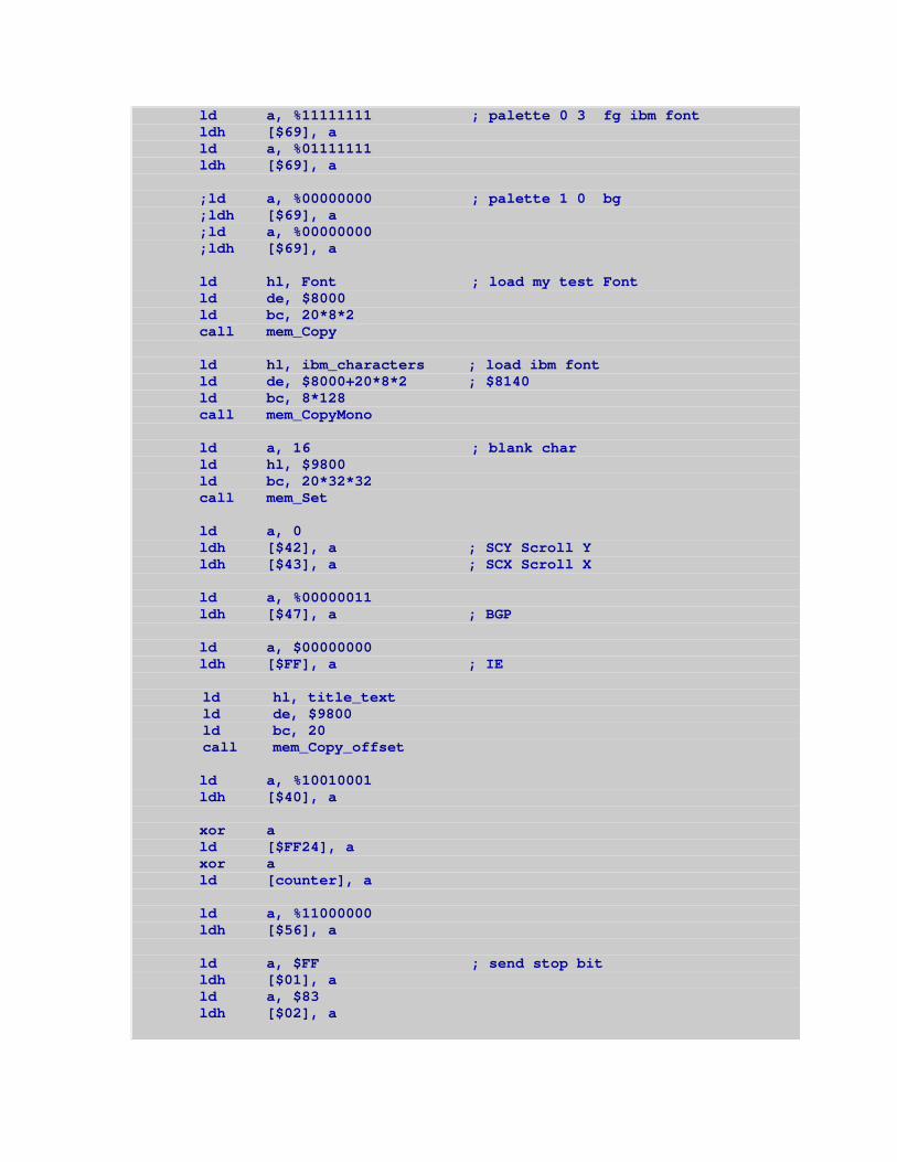
ld a, %11111111 ; palette 0 3 fg ibm font ldh [$69], a ld a, %01111111 ldh [$69], a ;ld a, %00000000 ; palette 1 0 bg ;ldh [$69], a ;ld a, %00000000 ;ldh [$69], a ld hl, Font ; load my test Font ld de, $8000 ld bc, 20*8*2 call mem_Copy ld hl, ibm_characters ; load ibm font ld de, $8000+20*8*2 ; $8140 ld bc, 8*128 call mem_CopyMono ld a, 16 ; blank char ld hl, $9800 ld bc, 20*32*32 call mem_Set ld a, 0 ldh [$42], a ; SCY Scroll Y ldh [$43], a ; SCX Scroll X ld a, %00000011 ldh [$47], a ; BGP ld a, $00000000 ldh [$FF], a ; IE ld hl, title_text ld de, $9800 ld bc, 20 call mem_Copy_offset ld a, %10010001 ldh [$40], a xor a ld [$FF24], a xor a ld [counter], a ld a, %11000000 ldh [$56], a ld a, $FF ; send stop bit ldh [$01], a ld a, $83 ldh [$02], a
ld a, IEF_HILO ldh [rIE], a ret wait_vb ldh a, [$44] cp 144 jp nz, wait_vb ret mem_Copy_offset:: inc b inc c jr .skip .loop ld a, [hl+] add a, 20 ; my offset hack ld [de], a inc de .skip dec c jr nz, .loop dec b jr nz, .loop ret ibm_characters chr_IBMPC1 1,8 Font: DW `01111100 DW `10000010 DW `10000010 DW `10000010 DW `10000010 DW `10000010 DW `01111100 DW `00000000 DW `00010000 DW `00110000 DW `00010000 DW `00010000 DW `00010000 DW `00010000 DW `00111000 DW `00000000 DW `01111100 DW `10000010 DW `00000010 DW `01111100 DW `10000000 DW `10000000 DW `11111110 DW `00000000
DW `01111100 DW `10000010 DW `00000010 DW `00011100 DW `00000010 DW `10000010 DW `01111100 DW `00000000 DW `00001100 DW `00010100 DW `00100100 DW `01000100 DW `11111110 DW `00000100 DW `00000100 DW `00000000 DW `11111110 DW `10000000 DW `10000000 DW `11111100 DW `00000010 DW `00000010 DW `11111100 DW `00000000 DW `01111100 DW `10000000 DW `10000000 DW `11111100 DW `10000010 DW `10000010 DW `01111100 DW `00000000 DW `11111110 DW `00000010 DW `00000100 DW `00001000 DW `00010000 DW `00010000 DW `00010000 DW `00000000 DW `01111100 DW `10000010 DW `10000010 DW `01111100 DW `10000010 DW `10000010 DW `01111100 DW `00000000 DW `01111100 DW `10000010
DW `10000010 DW `01111110 DW `00000010 DW `00000010 DW `01111100 DW `00000000 DW `00111000 DW `01000100 DW `10000010 DW `11111110 DW `10000010 DW `10000010 DW `10000010 DW `00000000 DW `11111100 DW `10000010 DW `10000010 DW `11111100 DW `10000010 DW `10000010 DW `11111100 DW `00000000 DW `00111100 DW `01000010 DW `10000000 DW `10000000 DW `10000000 DW `01000010 DW `00111100 DW `00000000 DW `11111000 DW `10000100 DW `10000010 DW `10000010 DW `10000010 DW `10000100 DW `11111000 DW `00000000 DW `11111110 DW `10000000 DW `10000000 DW `11111000 DW `10000000 DW `10000000 DW `11111110 DW `00000000 DW `11111110 DW `10000000 DW `10000000 DW `11111000
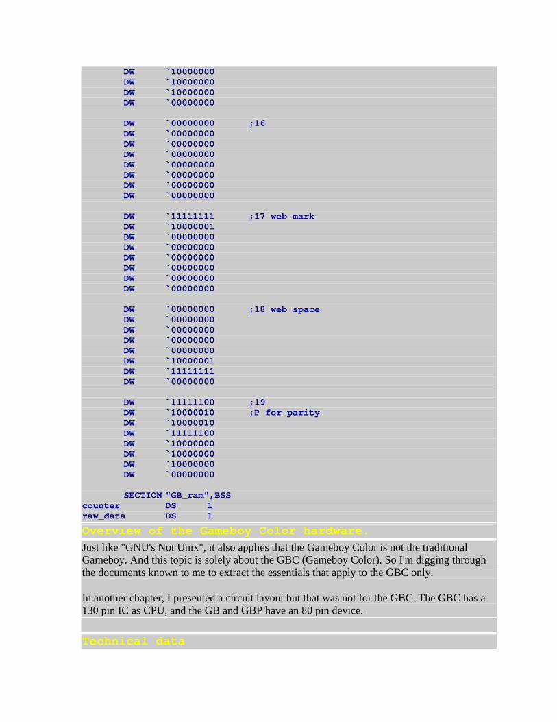
DW `10000000 DW `10000000 DW `10000000 DW `00000000 DW `00000000 ;16 DW `00000000 DW `00000000 DW `00000000 DW `00000000 DW `00000000 DW `00000000 DW `00000000 DW `11111111 ;17 web mark DW `10000001 DW `00000000 DW `00000000 DW `00000000 DW `00000000 DW `00000000 DW `00000000 DW `00000000 ;18 web space DW `00000000 DW `00000000 DW `00000000 DW `00000000 DW `10000001 DW `11111111 DW `00000000 DW `11111100 ;19 DW `10000010 ;P for parity DW `10000010 DW `11111100 DW `10000000 DW `10000000 DW `10000000 DW `00000000 SECTION "GB_ram",BSS counter DS 1 raw_data DS 1
Overview of the Gameboy Color hardware. Just like "GNU's Not Unix", it also applies that the Gameboy Color is not the traditional Gameboy. And this topic is solely about the GBC (Gameboy Color). So I'm digging through the documents known to me to extract the essentials that apply to the GBC only.
In another chapter, I presented a circuit layout but that was not for the GBC. The GBC has a 130 pin IC as CPU, and the GB and GBP have an 80 pin device. Technical data
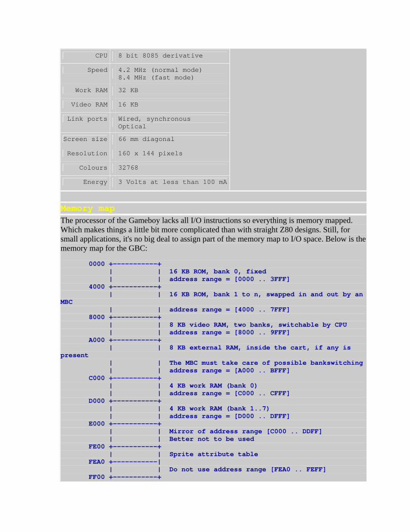
CPU 8 bit 8085 derivative
Speed 4.2 MHz (normal mode) 8.4 MHz (fast mode)
Work RAM 32 KB
Video RAM 16 KB
Link ports Wired, synchronous Optical
Screen size 66 mm diagonal
Resolution 160 x 144 pixels
Colours 32768
Energy 3 Volts at less than 100 mA Memory map The processor of the Gameboy lacks all I/O instructions so everything is memory mapped. Which makes things a little bit more complicated than with straight Z80 designs. Still, for small applications, it's no big deal to assign part of the memory map to I/O space. Below is the memory map for the GBC: 0000 +-----------+ | | 16 KB ROM, bank 0, fixed | | address range = [0000 .. 3FFF] 4000 +-----------+ | | 16 KB ROM, bank 1 to n, swapped in and out by an MBC | | address range = [4000 .. 7FFF] 8000 +-----------+ | | 8 KB video RAM, two banks, switchable by CPU | | address range = [8000 .. 9FFF] A000 +-----------+ | | 8 KB external RAM, inside the cart, if any is present | | The MBC must take care of possible bankswitching | | address range = [A000 .. BFFF] C000 +-----------+ | | 4 KB work RAM (bank 0) | | address range = [C000 .. CFFF] D000 +-----------+ | | 4 KB work RAM (bank 1..7) | | address range = [D000 .. DFFF] E000 +-----------+ | | Mirror of address range [C000 .. DDFF] | | Better not to be used FE00 +-----------+ | | Sprite attribute table FEA0 +-----------| | | Do not use address range [FEA0 .. FEFF] FF00 +-----------+
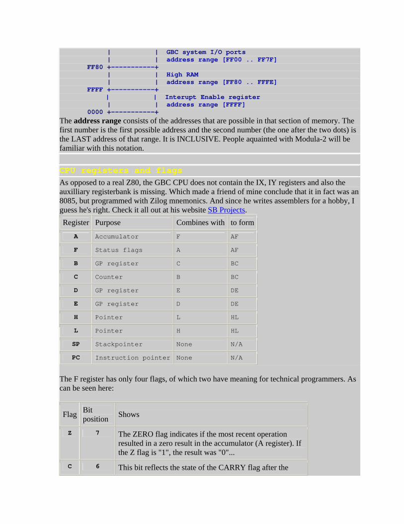
| | GBC system I/O ports | | address range [FF00 .. FF7F] FF80 +-----------+ | | High RAM | | address range [FF80 .. FFFE] FFFF +-----------+ | | Interupt Enable register | | address range [FFFF] 0000 +-----------+ The address range consists of the addresses that are possible in that section of memory. The first number is the first possible address and the second number (the one after the two dots) is the LAST address of that range. It is INCLUSIVE. People aquainted with Modula-2 will be familiar with this notation. CPU registers and flags As opposed to a real Z80, the GBC CPU does not contain the IX, IY registers and also the auxilliary registerbank is missing. Which made a friend of mine conclude that it in fact was an 8085, but programmed with Zilog mnemonics. And since he writes assemblers for a hobby, I guess he's right. Check it all out at his website SB Projects. Register Purpose Combines with to form
A Accumulator F AF
F Status flags A AF
B GP register C BC
C Counter B BC
D GP register E DE
E GP register D DE
H Pointer L HL
L Pointer H HL
SP Stackpointer None N/A
PC Instruction pointer None N/A
The F register has only four flags, of which two have meaning for technical programmers. As can be seen here:
Flag Bit position Shows
Z 7 The ZERO flag indicates if the most recent operation resulted in a zero result in the accumulator (A register). If the Z flag is "1", the result was "0"...
C 6 This bit reflects the state of the CARRY flag after the
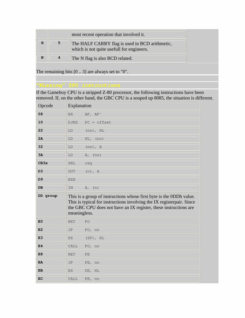
most recent operation that involved it.
H 5 The HALF CARRY flag is used in BCD arithmetic, which is not quite usefull for engineers.
N 4 The N flag is also BCD related.
The remaining bits [0 .. 3] are always set to "0". "Missing" Z80 instructions If the Gameboy CPU is a stripped Z-80 processor, the following instructions have been removed. If, on the other hand, the GBC CPU is a souped up 8085, the situation is different. Opcode Explanation
08 EX AF, AF'
10 DJNZ PC + offset
22 LD (nn), HL
2A LD HL, (nn)
32 LD (nn), A
3A LD A, (nn)
CB3x SRL reg
D3 OUT (n), A
D9 EXX
DB IN A, (n)
DD group This is a group of instructions whose first byte is the 0DDh value. This is typical for instructions involving the IX registerpair. Since the GBC CPU does not have an IX register, these instructions are meaningless.
E0 RET PO
E2 JP PO, nn
E3 EX (SP), HL
E4 CALL PO, nn
E8 RET PE
EA JP PE, nn
EB EX DE, HL
EC CALL PE, nn
ED group This is a group of instructions whose first byte is the 0EDh value. The involved instructions are: ADC HL, rp SBC HL, rp IN reg, (C) OUT reg, (C) NEG IMx RETI RETN CPI CPIR CPD CPDR IND INDR INI INIR LDD LDDR LDI LDIR OUTI OTIR OUTD OUTDR RLD RRD LD A, R LD R, A LD I, A LD A, I LD rp, (addr) LD (addr), BC LD (addr), DE LD (addr), HL
F0 RET P
F2 JP P, nn
F4 JP P, nn
F8 RET M
FA JP M, nn
FC CALL M, nn
FD group This is a group of instructions whose first byte is the 0FDh value. This is typical for instructions involving the IY registerpair. Since the GBC CPU does not have an IY register, these instructions are meaningless.
"Extra" instructions of the Gameboy CPU. Apart from removing Z80 instructions from the Z80 (if Nintendo started out with a Z80 anyway, which is not so sure at all) some instructions were added as well. The following table shows these instructions with their opcodes:
Opcode Instruction Explanation
08 LD (nn), SP Memory (nn) := SP
10 STOP Stop oscillator and put CPU in powersave mode
22 LDI (HL), A Memory (HL) := A; HL := HL + 1
2A LDI A, (HL) A := Memory (HL); HL := HL + 1
32 LDD (HL), A Memory (HL) := A; HL := HL - 1
3A LDD A, (HL) A := Memory (HL); HL := HL - 1
D9 RETI Return from interrupt. This is the last instruction from interrupt service routines.
E0 LD (FF00 + n), A Address := FF00 + n; Memory (Address) := A
E2 LD (FF00 + C), A Address := FF00 + Register (C); Memory (Address) := A
E8 ADD SP, nn SP := SP + nn nn = [-128 .. 127]
EA LD (nn), A Memory (nn) := A
F0 LD A, (FF00 + n) A := Memory (FF00 + n)
F2 LD A, (FF00 + C) A := Memory (FF00 + C register)
F8 LD HL, SP + dd HL := SP + dd dd = [-128 .. 127]
FA LD A, (nn) A := Memory (nn)
CB 3x SWAP loc Exchange the values of the bitgroups [0..3] and [4..7] within the location 'loc', which can be any 8 bit register or the 8 bits addressed by the HL registerpair.
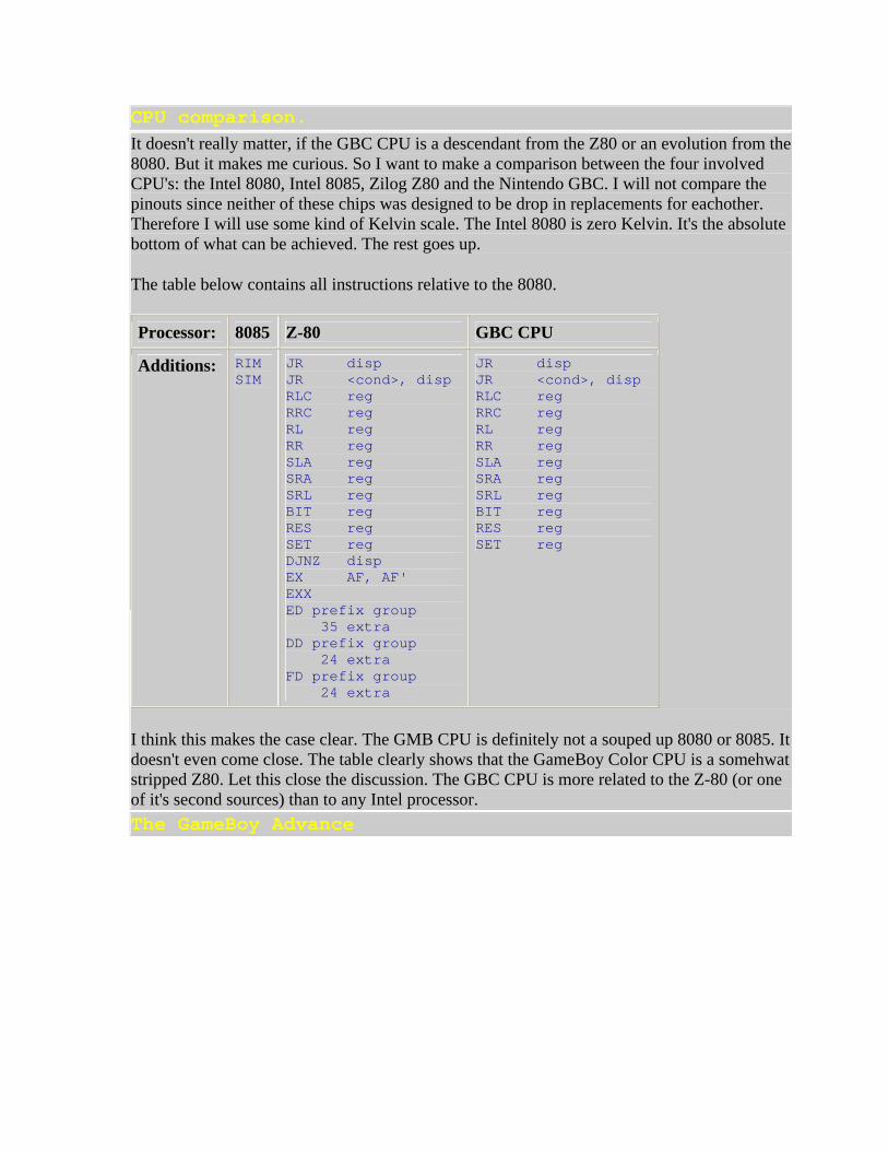
CPU comparison. It doesn't really matter, if the GBC CPU is a descendant from the Z80 or an evolution from the 8080. But it makes me curious. So I want to make a comparison between the four involved CPU's: the Intel 8080, Intel 8085, Zilog Z80 and the Nintendo GBC. I will not compare the pinouts since neither of these chips was designed to be drop in replacements for eachother. Therefore I will use some kind of Kelvin scale. The Intel 8080 is zero Kelvin. It's the absolute bottom of what can be achieved. The rest goes up.
The table below contains all instructions relative to the 8080.
Processor: 8085 Z-80 GBC CPU
Additions: RIM SIM
JR disp JR <cond>, disp RLC reg RRC reg RL reg RR reg SLA reg SRA reg SRL reg BIT reg RES reg SET reg DJNZ disp EX AF, AF' EXX ED prefix group 35 extra DD prefix group 24 extra FD prefix group 24 extra
JR disp JR <cond>, disp RLC reg RRC reg RL reg RR reg SLA reg SRA reg SRL reg BIT reg RES reg SET reg
I think this makes the case clear. The GMB CPU is definitely not a souped up 8080 or 8085. It doesn't even come close. The table clearly shows that the GameBoy Color CPU is a somehwat stripped Z80. Let this close the discussion. The GBC CPU is more related to the Z-80 (or one of it's second sources) than to any Intel processor. The GameBoy Advance
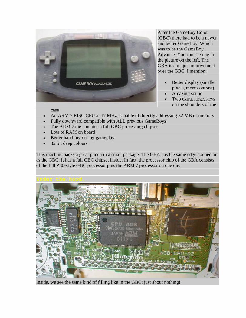
After the GameBoy Color (GBC) there had to be a newer and better GameBoy. Which was to be the GameBoy Advance. You can see one in the picture on the left. The GBA is a major improvement over the GBC. I mention:
• Better display (smaller pixels, more contrast)
• Amazing sound • Two extra, large, keys
on the shoulders of the case
• An ARM 7 RISC CPU at 17 MHz, capable of directly addressing 32 MB of memory • Fully downward compatible with ALL previous GameBoys • The ARM 7 die contains a full GBC processing chipset • Lots of RAM on board • Better handling during gameplay • 32 bit deep colours
This machine packs a great punch in a small package. The GBA has the same edge connector as the GBC. It has a full GBC chipset inside. In fact, the processor chip of the GBA consists of the full Z80-style GBC processor plus the ARM 7 processor on one die. Under the hood.
Inside, we see the same kind of filling like in the GBC: just about nothing!
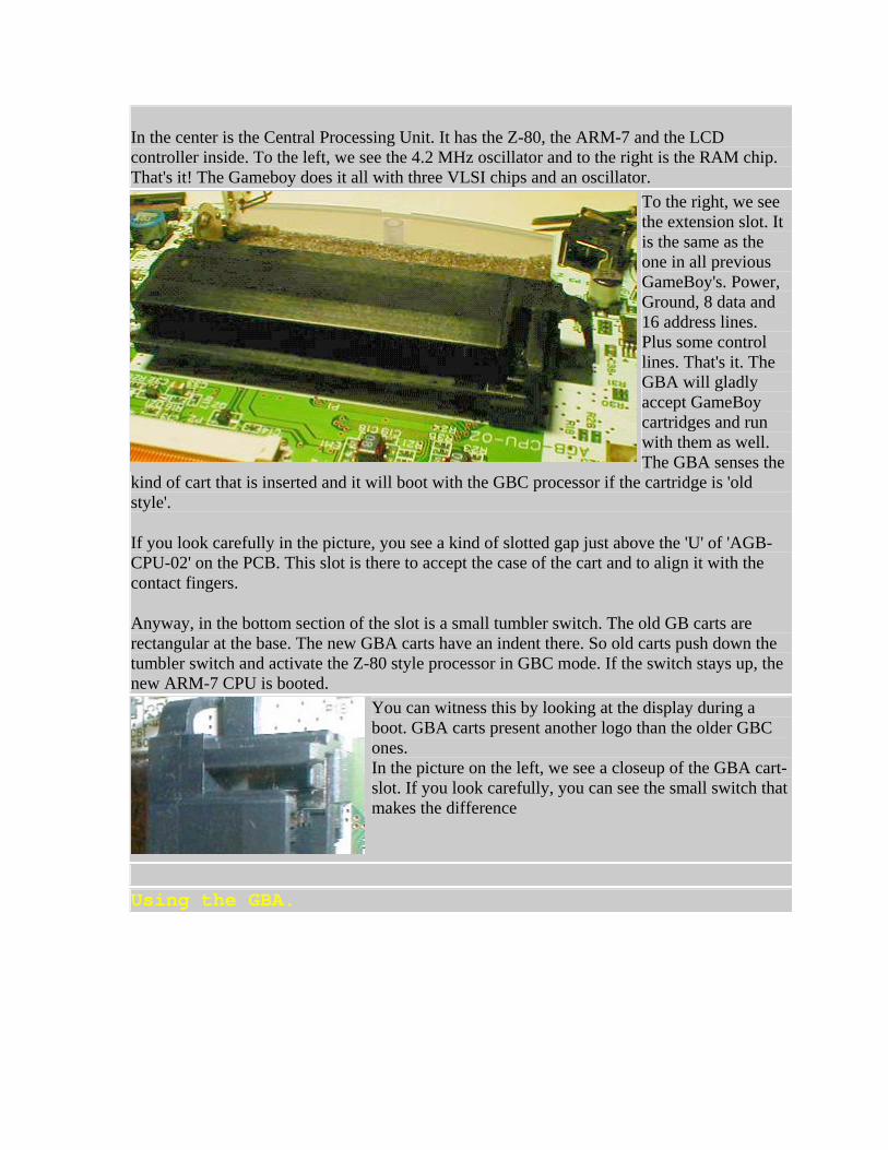
In the center is the Central Processing Unit. It has the Z-80, the ARM-7 and the LCD controller inside. To the left, we see the 4.2 MHz oscillator and to the right is the RAM chip. That's it! The Gameboy does it all with three VLSI chips and an oscillator.
To the right, we see the extension slot. It is the same as the one in all previous GameBoy's. Power, Ground, 8 data and 16 address lines. Plus some control lines. That's it. The GBA will gladly accept GameBoy cartridges and run with them as well. The GBA senses the
kind of cart that is inserted and it will boot with the GBC processor if the cartridge is 'old style'.
If you look carefully in the picture, you see a kind of slotted gap just above the 'U' of 'AGB-CPU-02' on the PCB. This slot is there to accept the case of the cart and to align it with the contact fingers.
Anyway, in the bottom section of the slot is a small tumbler switch. The old GB carts are rectangular at the base. The new GBA carts have an indent there. So old carts push down the tumbler switch and activate the Z-80 style processor in GBC mode. If the switch stays up, the new ARM-7 CPU is booted.
You can witness this by looking at the display during a boot. GBA carts present another logo than the older GBC ones. In the picture on the left, we see a closeup of the GBA cart-slot. If you look carefully, you can see the small switch that makes the difference
Using the GBA.

The GBA is wonderfull to play with. All the GBC games work 'out of the box', although the colours are quite different. The only drawback is that the pixels are smaller so the height of the image is smaller too. And there are black bars to the left and right of the playing field since the GBA has 250 pixels where the GBC has 'only' 160.
If you press the left shoulder button, the image is stretched to fill the screen horizontally. For some games (like V-rally) this is nice, but Pokemon Pinball gets harder to play. Press the right shoulder button and the image gets narrower again.
To the left we see the content of a GBA game cart. It is filled to the limit! They had to solder the Lithium cell on top of one of the memory chips to get everything in.
Look at the exge connector: it's the same as the one used in the GBC. Still, the ARM CPU is capable of addressing 32 MB of memory without an MBC unit. Apparently some kind of address multiplexing is required. I wonder how they do it...
To the right we see another GBA cart. This one has less crowded filling. It has only two integrated circuit
s to do it all. No battery required and still it keeps high scores and personal data.
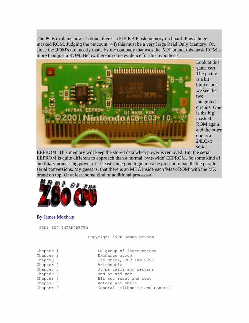
The PCB explains how it's done: there's a 512 KB Flash memory on board. Plus a huge masked ROM. Judging the pincount (44) this must be a very large Read Only Memory. Or, since the ROM's are mostly made by the company that uses the 'MX' brand, this mask ROM is more than just a ROM. Below there is some evidence for this hypothesis.
Look at this game cart. The picture is a bit blurry, but we see the two integrated circuits. One is the big masked ROM again and the other one is a 24LCxx serial
EEPROM. This memory will keep the stored data when power is removed. But the serial EEPROM is quite different to approach than a normal 'byte-wide' EEPROM. So some kind of auxilliary processing power or at least some glue logic must be present to handle the parallel - serial conversions. My guess is, that there is an MBC inside each 'Mask ROM' with the MX brand on top. Or at least some kind of additional processor.
By James Moxham
ZINT Z80 INTERPRETER
pyright 1996 James Moxham
apter 1 LD group of instructions
ontrol
Co
ChChapter 2 Exchange group
and PUSH Chapter 3 The stack, POP Chapter 4 Arithmetic
and returns Chapter 5 Jumps callsChapter 6 And or and xor
nd test Chapter 7 Bit set reset aChapter 8 Rotate and shift
c and cChapter 9 General arithmeti
Chapter 10 Block transfer and search Chapter 11 Input and Output instructions Chapter 12 Additional useful commands Chapter 13 Number bases Chapter 14 The flags Appendix 1 Binary, hex ascii decimal TC conversion
***************************************************************
A,6
This loads the A register with the number 6, so the register
CZPSNH BC DE HL IX IY A' CZPSNH' BC' DE' HL' SP
You can transfer this data to other registers
CZPSNH BC DE HL IX IY A' CZPSNH' BC' DE' HL' SP
pies the data in the A register to the H register. In fact H
data: Number bases
As most programmers of BASIC will know numbers can be
A,255 gives
DE HL IX IY A' CZPSNH' BC' DE' HL' SP
The H at the end signifies that the number is a hex number.
** CHAPTER 1 The LD instruction The LD instruction is perhaps the most useful instruction in the Z80. It is used to transfer data between registers, and to and from memory. The most simple type of LD instruction is to fill a register with a number: (Use F1) LD display now appears as A 06 000000 0000 0000 0000 0000 0000 00 000000 0000 0000 0000 0000 H,A LD
A 06 000000 0000 0000 0600 0000 0000 00 000000 0000 0000 0000 0000 cocould have been any one of A B C D E H or L. The data in the A register remaines unchanged. Transferring
represented in several forms, binary octal and hexadecimal being common bases. The registers in the above example display the data in hexadecimal form. Thus LD CZPSNH BC A
FF 000000 0000 0000 0000 0000 0000 00 000000 0000 0000 0000 0000 FF is 255 in hexadecimal. The equivalent statement using
hexadecimal directly is A,0FFH LD
The 0 at the front is necessary because the first digit in any number should always be between 0 and 9.
You can also use binary A,11111111B LD
where the B at the end specifies the number is a binary
The reason for using all three bases is because some
o other bases are supported, two's complement and direct ascii
B,073H
Double register LD's
HL,1000 returns
CZPSNH BC DE HL IX IY A' CZPSNH' BC' DE' HL' SP
can alse transfer this data from one double register pair to
BC,HL gives
DE HL IX IY A' CZPSNH' BC' DE' HL' SP
Transfers to and from memory
The above instructions all transfer data within the
A,255:LD HL,1000:LD,(HL) A
Here we are using more than one statement in a line. The
number. instructions are much easier to understand in one base. Twcharacters and are discussed in detail in ch16. The following instructions all do the same thing. LDLD B,01110011B LD B,65 LD B,"s" As you notice from the register display some registers have been grouped together. For example the H and L registers are displayed together as HL. You can treat these pairs as if they were one LD A 00 000000 0000 0000 03E8 0000 0000 00 000000 0000 0000 0000 0000 Weanother LD CZPSNH BC A
00 000000 03E8 0000 03E8 0000 0000 00 000000 0000 0000 0000 0000 The double registers can be any one of BC DE HL IX IY or SP.
microprocessor. The following sequence transfers a data to the memory (Use F1 or write as a program and then type F5) LD first two statements load the registers as we have seen before. The last statement loads memory location 1000 with 255. To retrieve this data we can use D,(HL) LD
which transfers 255 from the memory to register D.
see what is in the memory at any one time use the view
general the memory location is usually given by the HL
xt the data is transferred
(IX),72:LD (IX+1),69:LD (IX+2),76:LD (IX+3),76:LD (IX+4),79
e final way LD can be used is to transfer double registers to
(500),BC
ansfers the contents of C to the memory location 500 and the
DE,(500)
e register can be BC DE HL IX IY or SP.
e LD instructions
LD H,(IX+d)
Tomemory command. Inregister pair. The BC and DE regsters can be used as the memory location but the data can only be transferred to and from register A eg LD (BC),A is allowed but LD B,(DE) is not. A second way to transfer data to and from memory is to use a number instead of a register pair. Thus LD E,(38C1H) transfers to register E the data in memory 1000 LD (HL),34 transfers to the location stored in HL the no 34 A third way is to use the IX and IY registers. Say for example we want to store the word HELLO in memory. First we would look up the ASCII values for the letters, which are 72 69 76 76 79. We will store the word starting at memory location 500. First we load IX or IY with 500 LD IX,500 Ne LD e the view memory command to see where this data is. Us
Thand from memory. For example LD trcontents of B to location 501. We can load this data from memory to register pair DE with a LD Th at follows now is a list of all the possiblWh
sorted alphabetically. The letter n is used to indicate a number between 0 and 255 (0 and 0FFH). nn represents a number between 0 and 65535 (0 and 0FFFFH). d is any number between -127 and +127 (the +d can be -d; LD (IX-23) A (BC),A LD B,(HL) LD
LD (DE),A LD B,(IX+d) LD H,(IY+d) LD (HL),A LD B,(IY+d) LD H,A LD (HL),B LD B,A LD H,B LD (HL),C LD B,B LD H,C LD (HL),D LD B,C LD H,D LD (HL),E LD B,D LD H,E LD (HL),H LD B,E LD H,H

LD (HL),L LD B,H LD H,L LD (HL),n LD B,L LD H,n LD (IX+d),A LD B,n LD HL,(nn)
n)
n)
n)
)
**************************************************************
CHAPTER 2 The EX instructions
ioned so far the
LD (IX+d),B LD BC,(nn) LD HL,nn LD (IX+d),C LD BC,nn LD I,A LD (IX+d),D LD C,(HL) LD IX,(nLD (IX+d),E LD C,(IX+d) LD IX,nn LD (IX+d),H LD C,(IY+d) LD IY,(nn) LD (IX+d),L LD C,A LD IY,nn LD (IX+d),n LD C,B LD L,(HL) LD (IY+d),A LD C,C LD L,(IX+d) LD (IY+d),B LD C,D LD L,(IY+d) LD (IY+d),C LD C,E LD L,A LD (IY+d),D LD C,H LD L,B LD (IY+d),E LD C,L LD L,C LD (IY+d),H LD C,n LD L,D LD (IY+d),L LD D,(HL) LD L,E LD (IY+d),n LD D,(IX+d) LD L,H LD (nn),A LD D,(IY+d) LD L,L LD (nn),BC LD D,A LD L,n LD (nn),DE LD D,B LD R,A LD (nn),HL LD D,C LD SP,(nLD (nn),IX LD D,D LD SP,HL LD (nn),IY LD D,E LD SP,IX LD (nn),SP LD D,H LD SP,IY LD A,(BC) LD D,L LD SP,nn LD A,(DE) LD D,n LD A,(HL) LD DE,(nLD A,(IX+d) LD DE,nn LD A,(IY+d) LD E,(HL) LD A,(nn) LD E,(IX+d)LD A,A LD E,(IY+d) LD A,B LD E,A LD A,C LD E,B LD A,D LD E,C LD A,E LD E,D LD A,H LD E,E LD A,L LD E,H LD A,n LD E,L LD A,R LD E,n LD A,I LD H,(HL ** In addition to the registers we have ment
Z80 has several additional registers. The most important of these are the so called prime registers, which are designated A' BC' DE' and HL'. You cannot access these registers directly, but you can swap them with the ordinary registers. If you type in the following code LD BC,1234H:LD DE,5678H:LD HL,9ABCH the registers will appear CZPSNH BC DE HL IX IY A' CZPSNH' BC' DE' HL' SPA
00 000000 1234 5678 9ABC 0000 0000 00 000000 0000 0000 0000 0000

Now type in X whEX ich swaps BC DE and HL with the prime registers
CZPSNH BC DE HL IX IY A' CZPSNH' BC' DE' HL' SP
u can now work on the normal registers, eg
en you want to swap the registers back again use EXX
e EXX statement is very useful for storing variables you are
veral other commands exist that swap registers.
AF,AF'
aps the DE register and the HL register.
(SP),HL
l swap the memory contents pointed to by the SP register with
,5678H:LD (1000H),BC:LD SP,1000H then
register is swapped with the
change Commands
X EX (SP),HL
**************************************************************
Chapter 3 The Stack
A 00 000000 0000 0000 0000 0000 0000 00 000000 1234 5678 9ABC 0000 Yo LD BC,1111H Wh Thworking on without having to save them in memory. The equivalent store to memory for these three registers would take 3 LD statements. Other EX commands Se EX swaps the A register and the flags with the corresponding prime registers. It is commonly used with EXX. DE,HL EX
sw EXEX (SP),IX EX (SP),IY althe corresponding register. The equivalent code for EX (SP),HL could be HL,1234H:LD BCLD
LD BC,(1000H):LD (1000H),HL:LD HL,BC us in the case of EX (SP),HL the L Th
data at the memory location pointed to by the SP register, and the H register is swapped with the memory location + 1 pointed to by the SP register. Type MEMORY to check this. Ex EXEX AF,AF' EX (SP),IX EX DE,HL EX (SP),IY **

The memory of a computer can be thought of as a library, with each book representing a memory location. LD BC,(350) is like finding the 350th book. The stack on the other hand is like a pile of books. Instead of storing the BC register in memory location 350 and then retrieving it later we can put it on top of a pile of books, and take it off later. The following code shows how the stack works
SH BC takes the BC register and puts it on top of the pile
BC,0 clears the BC register, and
P BC takes the top book and puts it back in the BC register.
In fact the data in 502 and 503 could have been POP ed into
SH BC:POP DE
locations are used to store data you have to set
e PUSH and POP instruction both work on double register pairs
e stack commands
SH AF POP AF
LD BC,1234:LD SP,504H initialises the registers PUof books. LD PO If you now view the memory you can see what has happened. The SP register was used as a pointer as to where the top of the pile of books was. Thus after PUSH BC, 503H contains 12 or the H register, and 502 contains 34 or the L register. The SP was 502. POP BC put 502 into the L register and 503 into the H register, and added 2 to SP to make 504 again. any register. Try the dollowing to confirm this PU cause memoryBe
where you wnat the stack to be before using PUSH and POP. The stack was in this case set at 504 but could have been any location. The instruction LD SP,504 should occur before any PUSH or POP instructions are used and so usually appears near the beginning of a program. Most programs would use a maximum of 20 PUSH's before POP's so you need to make sure that about 40 memory locations below the initial value of the SP are not used. The ORG instruction is used to reserve this memory. Thonly. Thus for the purposes of this instruction the A register and the flag register are grouped together as an AF register, with the F register being the least significant byte. The way the individual flags are grouped in the F register is discussed in the chapter on the flags. Th PUPUSH BC POP BC PUSH DE POP DE
PUSH HL POP HL PUSH IX POP IX PUSH IY POP IY ****************************************************************** Chapter 4 Arithmetic
Arithmetic in machine code is a little different to
When two numbers are added or subtracted there needs to be a
e Z or Zero flag, which is set to 1 if the result is zero, and
e P flag is set when the parity is odd, and reset when it is
e S or Sign flag, which is set to 1 if the result of an
H or half carry flag, which is used when converting hex
Adding
e following code shows how to add two numbers.
CZPSNH BC DE HL IX IY A' CZPSNH' BC' DE' HL' SP
you now type ADD A,255 then the result will be
e carry flag has been set to indicate that the answer was
arithmetic in a higher level language such as BASIC or FORTRAN. Registers can be added, subtracted, but multiplication and division require a short program. Other instructions exist to compare two numbers and increment or decrement registers. way of signalling a carry or borrow if this has occurred. In addition to a carry five other features of the operation, such as = to zero and negative or positive are signalled. This is done using the flags, which are shown in the register display as CZPSNH. The six flags are covered briefly below and are covered in more detail in the chapter on the flags and on number basses. The C or carry flag is set if the result of an add is too great for the register to hold the value. In subtraction it is set if the answer is less than 0, necessitating a borrow. Threset to 0 if the result is not zero. Theven. It is also used by some instructions to signify overflow, and thus is sometimes written as the P/V flag. Thoperation is between 0 and 127, and reset to 0 if between 128 and 255. e Th
values to BCD. The N flag indicates whether the last instruction was an add or subtract. These flags are used by the DAA instruction. Th A,5:ADD A,3 will produce LD
A 08 000000 0000 0000 0000 0000 0000 00 000000 0000 0000 0000 0000 if A CZPSNH BC DE HL IX IY A' CZPSNH' BC' DE' HL' SP 07 100001 0000 0000 0000 0000 0000 00 000000 0000 0000 0000 0000 Th
greater than 255. If you now use ADD A,248 then the answer will be 0, and the Z
e 8 bit instructions all add either a number, or another
or carry flag 1 if answer >255 else 0
mplement else 0
f carry from bit 3 to bit 4 else 0
you want to add numbers that are more than the 0-255 that can
or carry flag 1 if answer >65535 else 0
f carry from bit 11 to bit 12 else 0
8 bit and 16 bit ADD instructions
IY,BC
Add with carry
is set of instructions are essentially the same as the ADD set,
flag will be set. Thregister to the A register. The flags are set on the result contained in the A register as follows. C Z or zero flag 1 if answer = 0 else 0 P flag 1 if overflow in twos coS or sign flag 1 if 127<answer<256 else 0 N flag 0 H or half carry flag 1 i 16 bit arithmetic Ifbe stored in the A register, then the HL, IX or IY registers can be used. Thus LD HL,1000H:LD BC,2000H:ADD HL,BC will give A CZPSNH BC DE HL IX IY A' CZPSNH' BC' DE' HL' SP 00 000000 2000 0000 3000 0000 0000 00 000000 0000 0000 0000 0000 The flags are set as follows. C Z or zero flag not changed P flag not changed S or sign flag not changed N flag 0 H or half carry flag 1 i D A,A ADD A,(HL) ADD HL,BC ADD AD
ADD A,B ADD A,(IX+d) ADD HL,DE ADD IY,DE ADD A,C ADD A,(IY+d) ADD HL,HL ADD IY,IY ADD A,D ADD HL,SP ADD IY,SP ADD A,E ADD IX,BC ADD A,H ADD IX,DE ADD A,L ADD IX,IX ADD A,n ADD IX,SP 8 bit group
Thbut add the carry flag as well. The instruction is ADC instead of ADD. Thus LD A 4:ADC A 3 would give an answer of 7 if the carry flag was 0, but an answer of 8 if the carry flag was 1 before the instruction.
The ADC instruction allows multiple precision adding. The least
or carry flag 1 if answer >255 else 0
se 0
f carry from bit 3 to bit 4 else 0
C A,A ADC A,B ADC A,C ADC A,D
e 16 bit ADC instructions use the HL register instead of the A
or carry flag 1 if answer >65536 else 0
7 else 0
f carry from bit 11 else 0
C HL,BC ADC HL,DE ADC HL,HL ADC HL,SP
Subtracting
The SUB group
SUB which is the opposite
B is used for 8 bit subtractions. The number or register is
mplement else 0
most significant bytes are added, and the carry is propogated to the next most significant bytes by using ADC. For the 8 bit ADC's using th A register the flags are affected C Z or zero flag 1 if result = 0 else 0 P flag 1 if TC <-128 or >127 elS or sign flag 1 if 127 < n < 256 else 0 N flag 0 H or half carry flag 1 i 8 bit ADC instructions ADADC A,E ADC A,H ADC A,L ADC A,n ADC A,(HL) ADC A,(IX+d) ADC A,(IY+d) 16 bit ADC group Thregister. The flags are affected as follows C Z or zero flag 1 if result = 0 else 0 P flag 1 if TC <-32768 or >3276S or sign flag 1 if 32767 < n < 65536 else 0 N flag 0 H or half carry flag 1 i 16 bit ADC group
AD ere are two subtraction instructions, Th
of ADD, and SBC which is subtract with borrow. Thus A,6:SUB 2 gives A = 4. LD
SUsubtracted from the A register and the result stored in the A register. One of the idiosyncracities of the Z80 instrcution set is that the A register is not written as it is with ADD, viz ADD A C but SUB C. In addition although there are 16 bit ADD's there are no 16 bit SUB's. (16 bit subtraction is done using the SBC instruction.) The flags are set as follows C or carry flag 1 if answer <0 else 0 Z or zero flag 1 if answer = 0 else 0 P flag 1 if overflow in twos coS or sign flag 1 if 127<answer<256 else 0

N flag 1 H or half carry flag 1 if borrow from bit 4 else 0 SUB instruction set
SUB A SUB B SUB C SUB D SUB E SUB H
Subtract with borrow
8 bit group
A,7:SBC A,3 gives A=4 if the carry flag was 0 and A=3 if it
e flags are affected as follows
else 0 se 0
f borrow from bit 12 else 0
C A,A SBC A,B SBC A,C SBC A,D
row
ese instructions subtract the designated register from the HL
answer < 0 else 0
8 else 0
f borrow from bit 12 else 0
16 bit SBC group
SBC HL,SP
Compares
e compare instruction can be thought of as an 8 bit SUB
contents of the A register remain unchanged. Thus
SUB L SUB n SUB (HL) SUB (IX+d) SUB (IY+d) The SBC instruction group is the opposite to the ADC group. The register or number is subvtracted from the A register, along with the C flag, and the result stored in the A register. Thus LDwas 1 before the SBC. Th C or carry flag 1 if <0 else 0 Z or zero flag 1 if result = 0 P flag 1 if TC >127 or <-128 elS or sign flag 1 if 127 < n <256 else 0 N flag 1 H or half carry flag 1 i SBSBC A,E SBC A,H SBC A,L SBC A,n SBC A,(HL) SBC A,(IX+d) SBC A,(IY+d) 16 bit subtracts with bor
Thregister pair and store the answer in the HL register pair. The flags are affected as follows or carry flag 1 if C
Z or zero flag 1 if result = 0 else 0 P flag 1 if TC >32767 or <-3276S or sign flag 1 if 32767 < n < 65536 else 0 N flag 1 H or half carry flag 1 i C HL,BC SBC HL,DE SBC HL,HL SB
Thinstruction in the way the flags are changed, except that the
LD A,9:CP 9 gives A CZPSNH BC DE HL IX IY A' CZPSNH' BC' DE' HL' SP 09 010010 0000 0000 0000 0000 0000 00 000000 0000 0000 0000 0000 where for example the zero flag has been set because 9 - 9 is zero, but the A register still contains the original 9. The set is CP A CP B CP C CP D CP E CP H CP L CP n CP (HL) CP (IX+d) CP (IY+d) Increment Increments are the same as adding a 1. Thus INC B is the same as LD A,B:ADD A,1:LD B,A. The results of all increments to single registers affect the flags as if an ADD had been perfomed. However for double register groups, such as INC BC the registers are unaffected. The first two columns are the 8 bit increments that do affect the flags, and the last column is the 16 bit increments that leave the flags unchanged. INC A INC (HL) INC BC INC B INC (IX+d) INC DE INC C INC (IY+d) INC HL INC D INC IX INC E INC IY INC H INC SP INC L Decrement These are the opposite to the increment group, the subtract 1 from the register in question. As before single register decrements affect the flags as a subtract would, but double register decrements leave the flags as they are. DEC A DEC (HL) DEC BC DEC B DEC (IX+d) DEC DE DEC C DEC (IY+d) DEC HL DEC D DEC IX DEC E DEC IY DEC H DEC SP DEC L **************************************************************** Chapter 5 Jumps Calls and Returns There are five instructions in this group. JP and JR are like GOTO in basic, and jump to the corresponding line. CALL is like GOSUB, and calls a subroutine. RET returns from the subroutine.
Jumps The simplest type of jump is demonstrated by the following short program. Line1: LD A,5:JP Line 3 Line2: end line3: LD B,6:END Line2 is never encountered because the program jumps to Line3. The next type of jump only occurs if the flag condition specified by the jump is true. Line1: LD A,0:LD B,5 Line2: ADD A,1:DEC B:JP NZ Line2 END Line1 loads B with 5. The program now loops through line2 until B is equal to 0. This is because JP NZ only jumps if the result of the last operation to affect the Z flag was not zero. Since the zero flag is set to 0 by DEC B if B is not equal to 0 the program loops until B=0. The following are the conditions that can be used with JP. NZ Jump if zero flag = 0. (last Z flag instr <>0) Z Jump if zero flag = 1. (last Z flag instr = 0) NC Jump if carry flag = 0. (last C instr = no carry) C Jump if carry flag = 1. (last C instr = carry) PO Jump if parity odd, parity flag = 0. PE Jump if parity even, parity flag = 1. P Jump if sign positive, sign flag = 0. M Jump if sign negative (minus), sign flag = 1. Relative jumps In the interpreter the JR instruction is the same as the JP instruction. However there is a difference between the two in the compiled program. The JR instruction, instead of storing the value of the location to be jumped to, instead stores a displacement value, which may be anything between +127 and -127. A displacement value of say -3 says jump to the instruction 3 bytes before this one. The reasoning behind this is that relative jumps take only two bytes of memory wheras ordinary jumps take three. However this memory saving is offset by the fact that ordinary jumps are quicker than relative jumps. In addition conditional jumps PO PE P and M are not allowed with JR. All this means that in practical terms it is probably better to ignore the JR instruction and to only use the JP instuction. DJNZ The third type of jump is the DJNZ instruction. The following
program shows how it works. Line1: LD A,0:LD B,5 Line2: ADD A,1:DJNZ Line2 END Line1 sets A to 0 and B to 5. Line2 adds one to A. The DJNZ subtracts one from register B, and if the result is not zero jumps to the location shown. Thus the program loops through 20 until B is 0, and then ends. Summary of Jump instructions JP nn JP Z,nn JP PE,nn JR NZ,nn JP (HL) JP NC,nn JP P,nn JR Z,nn JP (IX) JP C,nn JP M,nn JR NC,nn JP (IY) JP PO,nn JR nn JR C,nn JP NZ,nn DJNZ nn Calls Subroutines are called by a CALL and terminated by a RET. Start: LD A,5:CALL Subroutine END Subroutine:LD B,4:ADD A,B:RET The return location is stored in the stack. CALL's like jumps can be conditional, and the same rules apply. RET's can also be conditional. In addition there are two additional returns, RETI and RETN, which return from interupts and non maskable interrupts respectively. Since interrupts are not implemented on the interpreter these two instructions do nothing. They can be included if they will be used in the final compiled program. Summary CALL nn RET nn CALL NZ,nn RET NZ,nn CALL Z,nn RET Z,nn CALL NC,nn RET NC,nn CALL C,nn RET C,nn CALL PO,nn RET PO,nn CALL PE,nn RET PE,nn CALL P,nn RET P,nn CALL M,nn RET M,nn RETI RETN ************************************************************** Chapter 6 AND OR and XOR
These instructions all work on the A register and peform bit by bit comparisons with the appropriate register. For example LD A,1010000B:LD B,0000001B:OR B gives A CZPSNH BC DE HL IX IY A' CZPSNH' BC' DE' HL' SP A1 000100 0100 0000 0000 0000 0000 00 000000 0000 0000 0000 0000 AND OR and XOR perform bit by bit comparisons of the designated register and the A register according to the following rules. A register bit other register bit A bit set to AND 0 0 0 0 1 0 1 0 0 1 1 1 OR 0 0 0 0 1 1 1 0 1 1 1 1 XOR 0 0 0 0 1 1 1 0 1 1 1 0 The flags are also set by the result in the A register, the details of which are in Ch 17. Note that the AND command affects the H flag differently to the other two, however all the other flags are affected the same way. Instruction set (n is any number or label that can be resolved into an 8 bit number) AND A OR A XOR A AND B OR B XOR B AND C OR C XOR C AND D OR D XOR D AND E OR E XOR E AND H OR H XOR H AND L OR L XOR L AND n OR n XOR n ****************************************************************** Chapter 7 Bit set, reset and test The instructions in this group allow a specific bit in a register or memory location to be set to 1, reset to 0 or tested to see if it is 1 or 0.
SET LD C,0:SET 3,C sets byte 3 of register 3 to 1. The result is register C = 8 in hexadecimal. The following table shows how the bits are numbered in a byte. 01010101 76543210 Bit 7 on the left is the most significant bit and bit 0 on the right is the least significant. For 16 bit numbers bit 15 is on the left and bit 0 is on the right. The registers that can be set, reset or tested are A B C D E H L and the memory location pointed to by (HL) (IX+d) or (IY+d). RES The RES instruction is the opposite of the SET instruction, it changes the appropriate bit to 0. Thus LD H,11111111B:RES 5,H results in a value of 0DFH Flags are not affected by either the SET or RES instructions. BIT The BIT instruction is used to test whether a specific bit is a zero or a one. LD D,10101010B:BIT 5,D results in A CZPSNH BC DE HL IX IY A' CZPSNH' BC' DE' HL' SP 00 000001 0000 0000 0000 0000 0000 00 000000 0000 0000 0000 0000 The flags, which indicate the result of the test, are set as follows. C or carry flag not affected Z or zero flag 1 if bit is zero else 0 P or parity/overflow may be anything S or sign flag may be anything N or subtract flag 0 H or half carry flag 1 Summary of instructions SET 0,A SET 4,A RES 0,A RES 4,A BIT 0,A BIT 4,A
SET 0,B SET 4,B RES 0,B RES 4,B BIT 0,B BIT 4,B SET 0,C SET 4,C RES 0,C RES 4,C BIT 0,C BIT 4,C SET 0,D SET 4,D RES 0,D RES 4,D BIT 0,D BIT 4,D SET 0,E SET 4,E RES 0,E RES 4,E BIT 0,E BIT 4,E SET 0,H SET 4,H RES 0,H RES 4,H BIT 0,H BIT 4,H SET 0,L SET 4,L RES 0,L RES 4,L BIT 0,L BIT 4,L SET 0,(HL) SET 4,(HL) RES 0,(HL) RES 4,(HL) BIT 0,(HL) BIT 4,(HL) SET 0,(IX+d) SET 4,(IX+d) RES 0,(IX+d) RES 4,(IX+d) BIT 0,(IX+d) BIT 4,(IX+d) SET 0,(IY+d) SET 4,(IY+d) RES 0,(IY+d) RES 4,(IY+d) BIT 0,(IY+d) BIT 4,(IY+d) SET 1,A SET 5,A RES 1,A RES 5,A BIT 1,A BIT 5,A SET 1,B SET 5,B RES 1,B RES 5,B BIT 1,B BIT 5,B SET 1,C SET 5,C RES 1,C RES 5,C BIT 1,C BIT 5,C SET 1,D SET 5,D RES 1,D RES 5,D BIT 1,D BIT 5,D SET 1,E SET 5,E RES 1,E RES 5,E BIT 1,E BIT 5,E SET 1,H SET 5,H RES 1,H RES 5,H BIT 1,H BIT 5,H SET 1,L SET 5,L RES 1,L RES 5,L BIT 1,L BIT 5,L SET 1,(HL) SET 5,(HL) RES 1,(HL) RES 5,(HL) BIT 1,(HL) BIT 5,(HL) SET 1,(IX+d) SET 5,(IX+d) RES 1,(IX+d) RES 5,(IX+d) BIT 1,(IX+d) BIT 5,(IX+d) SET 1,(IY+d) SET 5,(IY+d) RES 1,(IY+d) RES 5,(IY+d) BIT 1,(IY+d) BIT 5,(IY+d) SET 2,A SET 6,A RES 2,A RES 6,A BIT 2,A BIT 6,A SET 2,B SET 6,B RES 2,B RES 6,B BIT 2,B BIT 6,B SET 2,C SET 6,C RES 2,C RES 6,C BIT 2,C BIT 6,C SET 2,D SET 6,D RES 2,D RES 6,D BIT 2,D BIT 6,D SET 2,E SET 6,E RES 2,E RES 6,E BIT 2,E BIT 6,E SET 2,H SET 6,H RES 2,H RES 6,H BIT 2,H BIT 6,H SET 2,L SET 6,L RES 2,L RES 6,L BIT 2,L BIT 6,L SET 2,(HL) SET 6,(HL) RES 2,(HL) RES 6,(HL) BIT 2,(HL) BIT 6,(HL) SET 2,(IX+d) SET 6,(IX+d) RES 2,(IX+d) RES 6,(IX+d) BIT 2,(IX+d) BIT 6,(IX+d)
SET 2,(IY+d) SET 6,(IY+d) RES 2,(IY+d) RES 6,(IY+d) BIT 2,(IY+d) BIT 6,(IY+d) SET 3,A SET 7,A RES 3,A RES 7,A BIT 3,A BIT 7,A SET 3,B SET 7,B RES 3,B RES 7,B BIT 3,B BIT 7,B SET 3,C SET 7,C RES 3,C RES 7,C BIT 3,C BIT 7,C SET 3,D SET 7,D RES 3,D RES 7,D BIT 3,D BIT 7,D SET 3,E SET 7,E RES 3,E RES 7,E BIT 3,E BIT 7,E SET 3,H SET 7,H RES 3,H RES 7,H BIT 3,H BIT 7,H SET 3,L SET 7,L RES 3,L RES 7,L BIT 3,L BIT 7,L SET 3,(HL) SET 7,(HL) RES 3,(HL) RES 7,(HL) BIT 3,(HL) BIT 7,(HL) SET 3,(IX+d) SET 7,(IX+d) RES 3,(IX+d) RES 7,(IX+d) BIT 3,(IX+d) BIT 7,(IX+d) SET 3,(IY+d) SET 7,(IY+d) RES 3,(IY+d) RES 7,(IY+d) BIT 3,(IY+d) BIT 7,(IY+d) **************************************************************** Chapter 8 Rotate and shift group The instructions in this chapter are concerned with shifting or rotating the bits in a particular register. For example 10001000 shifted right becomes 01000100 Rotate group There are four instructions that rotate the contents of the A register only. RLCA RLCA rotates the A register to the left one place. The 7th bit is put back into the 0 position. The 7th bit also goes to the carry flag. LD A,10011000B:RLCA gives A CZPSNH BC DE HL IX IY A' CZPSNH' BC' DE' HL' SP 31 100000 0000 0000 0000 0000 0000 00 000000 0000 0000 0000 0000 Use View Registers to see the value of A in binary= 00110001B The flags are affected as follows C or carry flag previous bit 7 value Z or zero flag not affected P or parity/overflow not affected
S or sign flag not affected N or subtract flag 0 H or half carry flag 0 The RLCA instruction can be represented symbolically as C <--- bbbbbbbb <- | | ------------- RLA The RLA instruction rotates left through the carry flag. --- C <--- bbbbbbbb <-- | | ------------- > ---------- The bits in the register are all rotated left, the 7th bit goes to the carry flag and the carry flag goes to bit 0. LD A,1 then RLA 9 times, looking at the value of A each time will clarify the operation of this instruction. Apart from the carry flag, the other flags are set as for RLCA. RRCA This rotates the register right in a similar way to RLCA. Symbolically ---> bbbbbbbb ---> C | | ------ < ----- The register is shifted right by one, and the 0 bit goes to the carry flag and to the 7th bit. Flags apart from the carry are as for RLCA. RRA The RRA rotates right through the carry flag ---> bbbbbbbb ---> C -- | | ----------- < --------- The register is shifted right by one, the 0 bit goes to the carry flag, and the carry flag goes to bit 7. Flags apart from the carry flag are as for RLCA. Rotates through other registers
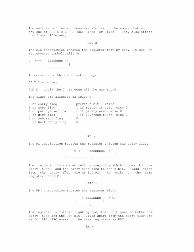
The next set of instructions are similar to the above, but act on any one of A B C D E H L (HL) (IX+d) or (IY+d). They also affect the flags differenty. RLC x The RLC instruction rotates the register left by one. It can be represented symbolically as C <--- bbbbbbbb <- | | ------------- To demonstrate this instruction type LD D,1 and then RLC D until the 1 has gone all the way round. The flags are affected as follows C or carry flag previous bit 7 value Z or zero flag 1 if result is zero, else 0 P or parity/overflow 1 if parity even, else 0 S or sign flag 1 if 127<result<256, else 0 N or subtract flag 0 H or half carry flag 0 RL x The RL instruction rotates the register through the carry flag. --- C <--- bbbbbbbb <-- | | ------------- > ---------- The register is rotated left by one, the 7th bit goes to the carry flag, and the carry flag goes to the 0 bit. Flags apart from the carry flag are as for RLC. RL works on the same registers as RLC. RRC x The RRC instruction rotates the register right. ---> bbbbbbbb ---> C | | ------ < ----- The register is rotated right by one, the 0 bit goes to bothe the carry flag and the 7th bit. Flags apart from the carry flag are as for RLC. RRC works on the same registers as RLC. RR x

The RR instruction rotates the register right through the carry flag. ---> bbbbbbbb ---> C -- | | ----------- < --------- The register is rotated right by one, the 0 bit goes to the carry flag and the carry flag goes to the 7th bit. The four bit rotate group There are two instructions in this group that rotate groups of bits through the A register and a memory location pointed to by the (HL) register. RLD The RLD instruction takes groups of four bits and rotates them as shown symbolically. ----->----- -------->---------- 12 ---<--- 34 or 1 2 -----<---- 3 <-- 4 ^| - A (HL) A (HL) The register on the left is the A register and the register on the right is a memory location pointed to by the HL register. The 4 least significant bits of the A register are moved to the 4 least significant bits of the (HL) location. The 4 least significant bits of the (HL) location are moved to the 4 most significant bits of the (HL) location. The 4 most significant bits of the (HL) location are moved to the 4 least significant bits of the A register. The 4 most significant bits of the A register remain unchanged. LD A,12H:LD HL,1000H:LD (HL),34H sets up the registers as shown above. RLD results in A CZPSNH BC DE HL IX IY A' CZPSNH' BC' DE' HL' SP 13 000000 0000 0000 0000 0000 0000 00 000000 0000 0000 0000 0000 with View Memory giving address 1000H = to 42H. The flags are set as follows C or carry flag not affected Z or zero flag 1 if result is zero, else 0 P or parity/overflow 1 if parity even, else 0 S or sign flag 1 if 127<result<256, else 0 N or subtract flag 0 H or half carry flag 0
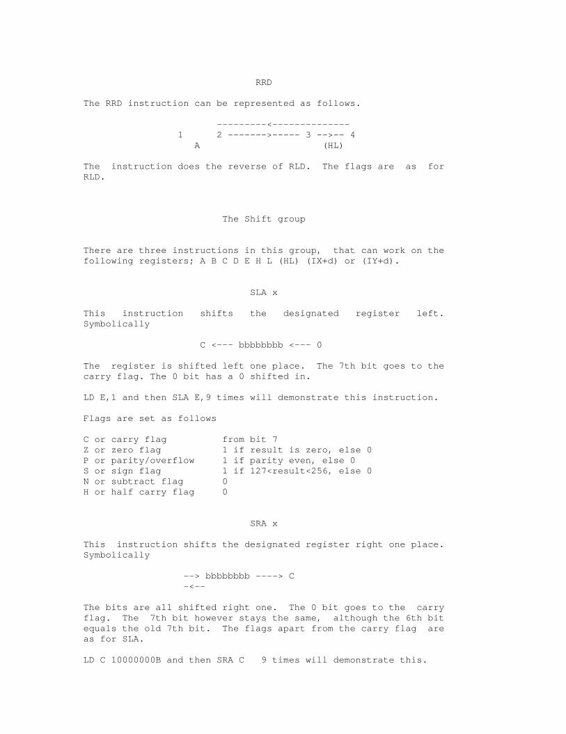
RRD The RRD instruction can be represented as follows. ---------<-------------- 1 2 ------->----- 3 -->-- 4 A (HL) The instruction does the reverse of RLD. The flags are as for RLD. The Shift group There are three instructions in this group, that can work on the following registers; A B C D E H L (HL) (IX+d) or (IY+d). SLA x This instruction shifts the designated register left. Symbolically C <--- bbbbbbbb <--- 0 The register is shifted left one place. The 7th bit goes to the carry flag. The 0 bit has a 0 shifted in. LD E,1 and then SLA E,9 times will demonstrate this instruction. Flags are set as follows C or carry flag from bit 7 Z or zero flag 1 if result is zero, else 0 P or parity/overflow 1 if parity even, else 0 S or sign flag 1 if 127<result<256, else 0 N or subtract flag 0 H or half carry flag 0 SRA x This instruction shifts the designated register right one place. Symbolically --> bbbbbbbb ----> C -<-- The bits are all shifted right one. The 0 bit goes to the carry flag. The 7th bit however stays the same, although the 6th bit equals the old 7th bit. The flags apart from the carry flag are as for SLA. LD C 10000000B and then SRA C 9 times will demonstrate this.
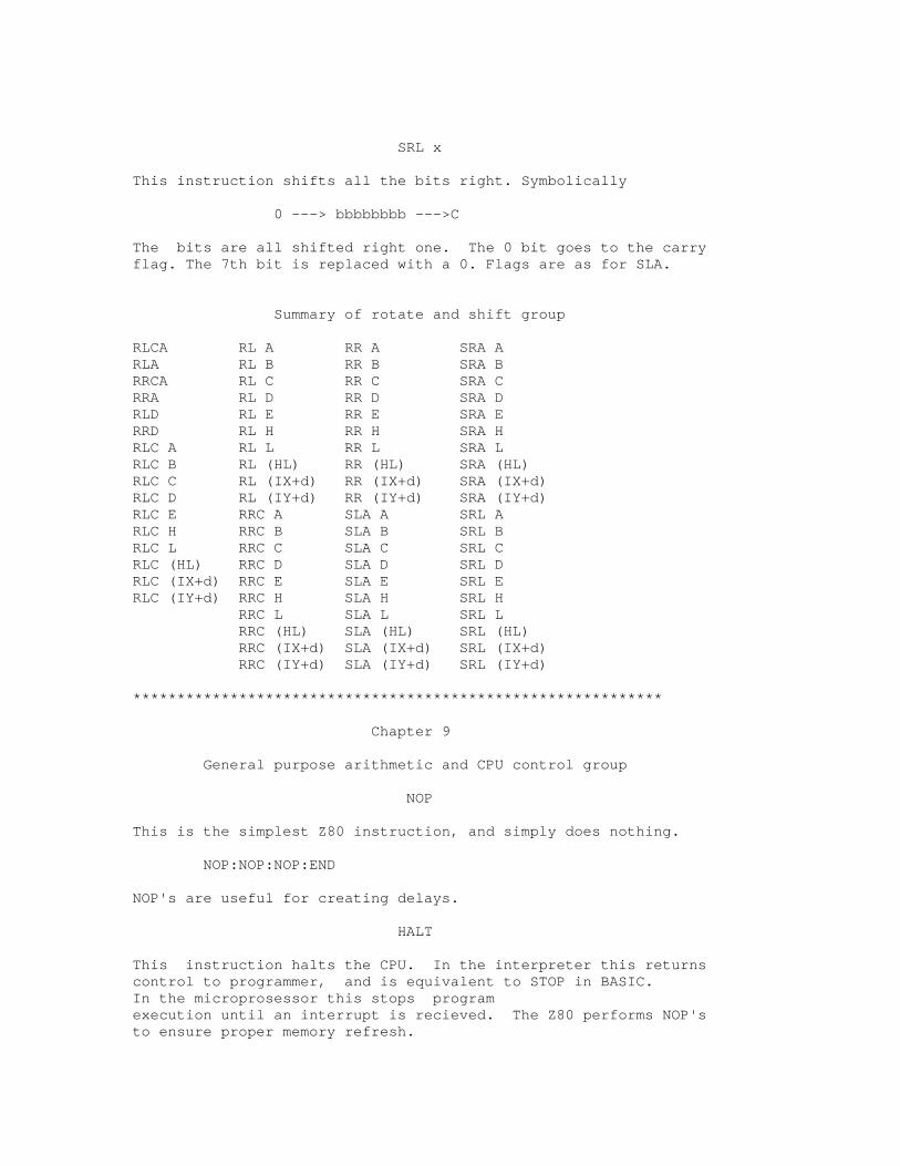
SRL x This instruction shifts all the bits right. Symbolically 0 ---> bbbbbbbb --->C The bits are all shifted right one. The 0 bit goes to the carry flag. The 7th bit is replaced with a 0. Flags are as for SLA. Summary of rotate and shift group RLCA RL A RR A SRA A RLA RL B RR B SRA B RRCA RL C RR C SRA C RRA RL D RR D SRA D RLD RL E RR E SRA E RRD RL H RR H SRA H RLC A RL L RR L SRA L RLC B RL (HL) RR (HL) SRA (HL) RLC C RL (IX+d) RR (IX+d) SRA (IX+d) RLC D RL (IY+d) RR (IY+d) SRA (IY+d) RLC E RRC A SLA A SRL A RLC H RRC B SLA B SRL B RLC L RRC C SLA C SRL C RLC (HL) RRC D SLA D SRL D RLC (IX+d) RRC E SLA E SRL E RLC (IY+d) RRC H SLA H SRL H RRC L SLA L SRL L RRC (HL) SLA (HL) SRL (HL) RRC (IX+d) SLA (IX+d) SRL (IX+d) RRC (IY+d) SLA (IY+d) SRL (IY+d) ************************************************************ Chapter 9 General purpose arithmetic and CPU control group NOP This is the simplest Z80 instruction, and simply does nothing. NOP:NOP:NOP:END NOP's are useful for creating delays. HALT This instruction halts the CPU. In the interpreter this returns control to programmer, and is equivalent to STOP in BASIC. In the microprosessor this stops program execution until an interrupt is recieved. The Z80 performs NOP's to ensure proper memory refresh.
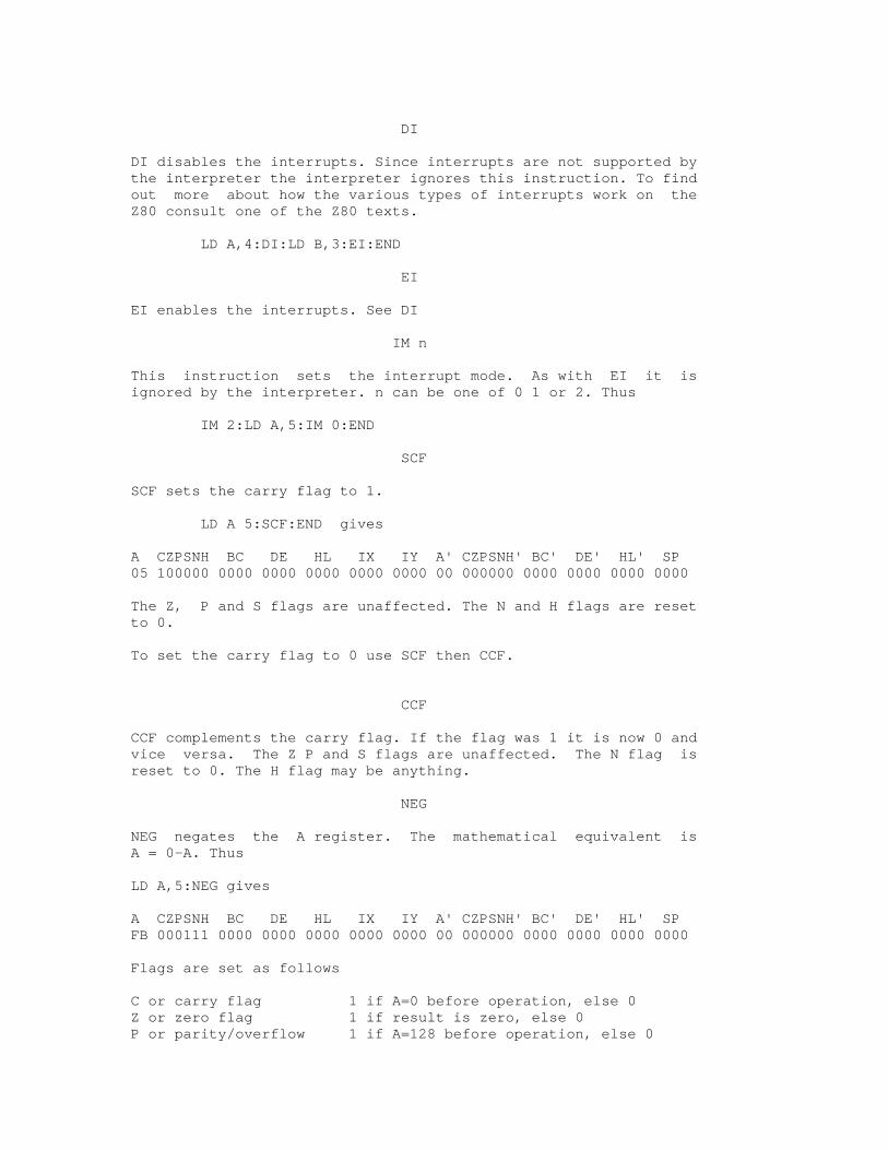
DI DI disables the interrupts. Since interrupts are not supported by the interpreter the interpreter ignores this instruction. To find out more about how the various types of interrupts work on the Z80 consult one of the Z80 texts. LD A,4:DI:LD B,3:EI:END EI EI enables the interrupts. See DI IM n This instruction sets the interrupt mode. As with EI it is ignored by the interpreter. n can be one of 0 1 or 2. Thus IM 2:LD A,5:IM 0:END SCF SCF sets the carry flag to 1. LD A 5:SCF:END gives A CZPSNH BC DE HL IX IY A' CZPSNH' BC' DE' HL' SP 05 100000 0000 0000 0000 0000 0000 00 000000 0000 0000 0000 0000 The Z, P and S flags are unaffected. The N and H flags are reset to 0. To set the carry flag to 0 use SCF then CCF. CCF CCF complements the carry flag. If the flag was 1 it is now 0 and vice versa. The Z P and S flags are unaffected. The N flag is reset to 0. The H flag may be anything. NEG NEG negates the A register. The mathematical equivalent is A = 0-A. Thus LD A,5:NEG gives A CZPSNH BC DE HL IX IY A' CZPSNH' BC' DE' HL' SP FB 000111 0000 0000 0000 0000 0000 00 000000 0000 0000 0000 0000 Flags are set as follows C or carry flag 1 if A=0 before operation, else 0 Z or zero flag 1 if result is zero, else 0 P or parity/overflow 1 if A=128 before operation, else 0
S or sign flag 1 if 127<result<256, else 0 N or subtract flag 1 if borrow from bit 4 else 0 H or half carry flag 1 CPL CPL complements the A register. All 0's become 1's and all 1's 0's. The C, Z P and S flags are all unaffected. The N and H flags are both set to 1. DAA DAA decimally adjusts the accumulator. This instruction allows decimal numbers to be added. For example let us add 11H and 22H LD A,11H:ADD A,22H which gives A = 33H However if we add 22H and 39H LD A,22H:ADD A,39H we get A = 5BH The B is illegal in decimal, or BCD, and is corrected by using DAA. Thus LD A 22H:ADD A 39H:DAA gives A = 61H, which is correct. Other examples LD A,91H:ADD A,92H unadjusted gives 23H, adjusted with DAA gives 83H and carry = 1 (use to get 183) LD A,99H:ADD A,99H unadjusted gives 32H, adjusted with DAA gives 98H and carry = 1. DAA also can be used after subtraction LD A,99H:SUB A,11H unadjusted gives 88H, adjusted with DAA gives 88H. LD A,91H:SUB A,19H unadjusted gives 78H, adjusted with DAA gives 72H. LD A,19H:SUB A,91H unadjusted gives 88H, adjusted with DAA gives 28H and carry = 1. (carry is used as borrow in subtracts) LD A,11H:SUB A,99H unadjusted gives 78H, adjusted with DAA gives 12 and carry = 1. The way DAA works is to selectively add numbers according to the value in A, and to the C H and N flags. In fact this is the purpose of the H and N flags as no other instruction uses them. The value added is given by the following table, although it is not necessary to understand or even to have the table to use DAA. DAA should always be used immediately after the ADD or SUB instruction to avoid flags being changed. DAA can also be used
with ADC INC SBC DEC NEG etc. N C Value of H Value of Hex no C flag after high nibble low nibble added execution 0 0 0-9 0 0-9 00 0 0 0 0-8 0 A-F 06 0 0 0 0-9 1 0-3 06 0 0 0 A-F 0 0-9 60 1 0 0 9-F 0 A-F 66 1 0 0 A-F 1 0-3 66 1 0 1 0-2 0 0-9 60 1 0 1 0-2 0 A-F 66 1 0 1 0-3 1 0-3 66 1 1 0 0-9 0 0-9 00 0 1 0 0-8 1 6-F FA 0 1 1 7-F 0 0-9 A0 1 1 1 6-F 1 6-F 9A 1 Flags are affected by DAA as follows C or carry flag as per table Z or zero flag 1 if A=0 else 0 P or parity/overflow 1 if parity even else 0 S or sign flag 1 if msb A = 1 else 0 N or subtract flag unaffected H or half carry flag may be anything Chapter 11 Block transfer and search group Four instructions exist in the Z80 instruction set that are used to transfer blocks of data from one memory location to another. Another set of four instructions allow searches through a set or memory locations for a specific byte. Block transfer group; LDI LDD LDIR LDDR LDI LDI moves a block of data. HL is the memory location to move from, DE is the memory location to move to and BC is the number of bytes to move. memory contents (DE) = memory contents (HL) DE = DE + 1 HL = HL + 1 BC = BC - 1 At the end of each loop the P flag indicates if BC is 0 (P=1 if <>0 and 0 if = to 0) C, Z and S flags are not affected H and N flags are reset to 0 P flag =1 if after LDI BC is not equal to 0, else P = 0
LDD LDD is the same as LDI except that the DE and HL registers are decremented. Thus (DE) = (HL) DE = DE - 1 HL = HL - 1 BC = BC - 1 The flags are the same as for LDI. Thus the program above would be rewritten LDIR This is the automatic version of LDI. Set the HL, DE and BC registers and then run LDIR. If BC is a high value the instruction can take a while to execute. LDIR does the following (DE) = (HL) DE = DE + 1 HL = HL + 1 BC = BC - 1 and repeats until BC = 0 Flags are a little different; C, Z and S unchanged H, N and P = 0 LDDR This instruction is the automatic version of LDD. The summary is (DE) = (HL) DE = DE - 1 HL = HL - 1 BC = BC - 1 and repeat until BC = 0 Flags are as for LDIR. The question may be asked; why use LDI when LDIR does the operation automatically. The reason is that the registers can be changed when using LDI. For instance you can transfer every alternate bytethis program transfers every alternate byte between instructions by inserting say a INC HL. oooOOOooo Block search group The next four instructions are concerned with searching for bytes in a block of data.
CPI CPI searches starting at the memory location pointed to by the HL register, and searches for BC number of bytes for the byte in register A. A - (HL) and set flags on the result of this compare, equivalent to CP (HL) HL = HL + 1 BC = BC - 1 The flags are set as follows C = no change Z = 1 if A - (HL) = 0 else 0 P = 1 if BC <> 0 after instruction else 0 S = 1 if sign A - (HL) negative in two's comp, else 0 H = 1 if a half carry from A - (HL) N = 1 CPD CPD is the same as CPI except that the HL register is decremented; HL = HL - 1. The flags are as for CPI. CPIR This is the automatic version of CPI. The instruction repeats until either A = (HL) or BC = 0. The flags are as for CPI. CPDR This is the automatic version of CPD. Flags are as for CPI. *************************************************************** Chapter 11 Input and output The Z80 has several comands that input and output data to the ports. However many of these are not very useful, and only one input and one output instruction are used in most Z80 computers. These are the IN A (n) and OUT (n) A instructions, where n is the port number between 0 and 255. Inputs and outputs do nothing on the ZINT interpreter, as these depend on the actual hardware used. OTDR INDR OTIR INIR OUTD IND OUTI INI OUT (C),A IN A,(C) OUT (C),B IN B,(C) OUT (C),C IN C,(C)
OUT (C),D IN D,(C) OUT (C),E IN E,(C) OUT (C),H IN H,(C) OUT (C),L IN L,(C) OUT (n),A IN A,(n) *************************************************************** Chapter 12 Addtional commands Apart from the instructions that generate code, there are additional commands which are needed to test and run the programs. These shall be looked at in alphabetical order. The semicolon ; The semicolon is used to indicate a remark. These are ignored by the program. LD A,5:; This loads the A register with 5:LD B,3:END Instructions can be added after the remark, as is the LD B,3. END END is used to indicate the end of a program. It should always be the last statement in a program, otherwise an error message will appear. EQU EQU is used to set labels to particular values. VARIABLE1 EQU 46H Later in the program, instead of writing say LD A,46H, we can write LD A,VARIABLE1. This enables the way the program works to be made a lot clearer. The label used, in this case VARIABLE1 can be any sequence of letters or numbers, but should be 3 or more letters long. Thus EQU X 5 is not allowed. The number can be decimal, hex or binary number. To see what the current values of the labels are the View Label command is used. Labels should be assigned values before they are encountered in the program. The value of a label cannot be changed once it has been assigned. ORG ORG is used to set the origin of the program when it is compiled. When the program is finally dumped into a Z80 computer's memory,
some way of indicating where the program will start is needed. In the Z80 it is customary to start the program not in memory location 0 but at memory location 100H. The first instruction in the program is a jump to location 100H. This is because the interrupts jump to locations between 5H and 100H. Thus a standard way to start a program is ORG 0:JP 100H:ORG 100H LD A,5 etc... the interrupts themselves are usually jumps also. Thus the interrupt at location 66H could be set by ORG 66H:JP Interrupt Interrupt:LD A,5 etc program to service interrupt. ORG is probably best ignored until you are familiar with the other instructions, as it is not necessary to write simple programs. *************************************************************** Chapter 13 Number Bases This chapter explains the number bases that are used by the interpreter. The appendix contains all the conversions from 0 to 255. For numbers larger than this the BASE command can be used. The bases to be cavered are binary, hexadecimal and two's complement. Binary Binary is the system of counting used by computers as it only has two digits, 0 and 1. A number in binary is written with a B on the end to differentiate it from the other bases; 1011B Hexadecimal Hexadecimal or Hex numbers use a base of 16, rather than 10 used in the decimal system. The digits used are 0 1 2 3 4 5 6 7 8 9 A B C D E F Hex numbers have a H on the end. In addition all H numbers should start with a number from 0 to 9 to distinguish them from text. A 0 is usually added to the beginning for this reason. Some examples of hex numbers are 0D3H 0FFH 012H 0ABCDH 28E6H 0H Two's complement Two's complement is a number system that ranges from -128 to +127. The result of the sum in two's complement is used to set one of the registers in the Z80; the overflow register. Numbers from 0 to 127 in decimal are the same in twos complement. However from 128 to 255 all two's complement numbers are negative. TC numbers are calculated by subtracting 256 from the dicimal number if the decimal number is between 128 and 255
inclusive. Thus 255 is -1 in TC, 128 is -128 and 45 is 45. There is no special ending to distinguish TC numbers, the - sign is all that is needed. Other bases Other bases such as octal are not used by the interpreter. ASCII symbols may be used providing they are in the range 32 to 127. They are written in quotes, thus LD A "s" results in A being 73 hex or 115 decimal, which is the ascii value for small s. ***************************************************************** Chapter 14 The flags This chapter discusses the 6 flags used by the Z80, and the conditions which affect them. The flags are represented in the register display by the symbols CZPSNH. The Z or zero flag The Z flag is set to 1 of the result of an operation is 0. If the result is other than 0 then the Z flag is reset to 0. The table below summarizes the instructions that affect the Z flag. Group Instruction Action 8 bit LD A I Z = 1 if register = 0 else 0 load group LD A R Z = 1 if register = 0 else 0 Search group CPI, CPIR, Z = 1 if A = (HL) else 0 CPD, CPDR ADD A x Z = 1 if register = 0 else 0 ADC A x " SUB x " SBC A x " AND x " 8 bit OR x " arithmetic XOR x " group CP x " INC x " DEC x " General purpose DAA " arithmetic group NEG " 16 bit ADC HL xx " arithmetic group SBC HL xx " RLC x " RL x " RRC x " Rotate and RR x " shift group SLA x " SRA x " SRL x "
RLD " RRD " Bit test group BIT n x Z = 1 if bit = 0 else 0 Input and INR (C) Z = 1 if input data =0 else 0 output group INI, IND, Z = 1 if B-1=0 else 0 INIR, INDR, Z = 1 OUTI, OUTD, Z = 1 if B-1=0 else 0 OTIR, OTDR Z = 1 The S or sign flag The sign flag is used to indicate whether in twos complement notation a number is negative or positive. (see chapter 16 for more about two's complement) Thus if the number is negative (- 128 to -1) then the sign flag is set to 1. If the number is positive (0 to 127) then the sign flag is reset to 0. Group Instruction Action 8 bit LD A I S = 1 if I register negative else 0 load group LD A R S = 1 if R register negative else 0 Search CPI,CPIR, S = 1 if result negative else 0 group CPD,CPDR " ADD A x " ADC A x " SUB x " 8 bit SBC A x " arithmetic AND x " group OR x " XOR x " CP x " INC x " DEC x " General purp DAA " arithmetic NEG " 16 bit ADC HL xx " arithmetic SBC HL xx " RLC x " RL x " RRC x " Rotate and RR x " shift group SLA x " SRA x " SRL x " RLD x S = 1 if A negative else 0 RRD x S = 1 if A negative else 0 Bit test gp BIT n x may be anything / IN R (C) S = 1 if input data negative else 0
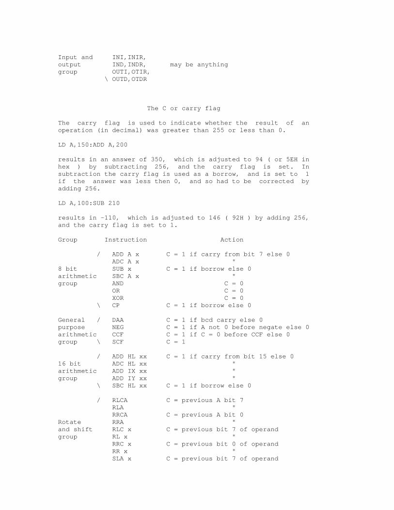
Input and INI,INIR, output IND,INDR, may be anything group OUTI,OTIR, \ OUTD,OTDR The C or carry flag The carry flag is used to indicate whether the result of an operation (in decimal) was greater than 255 or less than 0. LD A,150:ADD A,200 results in an answer of 350, which is adjusted to 94 ( or 5EH in hex ) by subtracting 256, and the carry flag is set. In subtraction the carry flag is used as a borrow, and is set to 1 if the answer was less then 0, and so had to be corrected by adding 256. LD A,100:SUB 210 results in -110, which is adjusted to 146 ( 92H ) by adding 256, and the carry flag is set to 1. Group Instruction Action / ADD A x C = 1 if carry from bit 7 else 0 ADC A x " 8 bit SUB x C = 1 if borrow else 0 arithmetic SBC A x " group AND C = 0 OR C = 0 XOR C = 0 \ CP C = 1 if borrow else 0 General / DAA C = 1 if bcd carry else 0 purpose NEG C = 1 if A not 0 before negate else 0 arithmetic CCF C = 1 if C = 0 before CCF else 0 group \ SCF C = 1 / ADD HL xx C = 1 if carry from bit 15 else 0 16 bit ADC HL xx " arithmetic ADD IX xx " group ADD IY xx " \ SBC HL xx C = 1 if borrow else 0 / RLCA C = previous A bit 7 RLA " RRCA C = previous A bit 0 Rotate RRA " and shift RLC x C = previous bit 7 of operand group RL x " RRC x C = previous bit 0 of operand RR x " SLA x C = previous bit 7 of operand
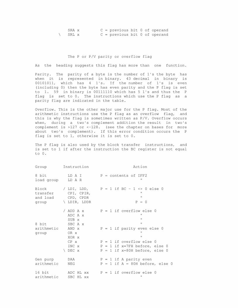
SRA x C = previous bit 0 of operand \ SRL x C = previous bit 0 of operand The P or P/V parity or overflow flag As the heading suggests this flag has more than one function. Parity. The parity of a byte is the number of 1's the byte has when it is represented in binary. 43 decimal in binary is 00101011, which has 4 1's. If the number of 1's is even (including 0) then the byte has even parity and the P flag is set to 1. 59 in binary is 00111110 which has 5 1's and thus the P flag is set to 0. The instructions which use the P flag as a parity flag are indicated in the table. Overflow. This is the other major use for the P flag. Most of the arithmetic instructions use the P flag as an overflow flag, and this is why the flag is sometimes written as P/V. Overflow occurs when, during a two's complement addition the result in two's complement is >127 or <-128. (see the chapter on bases for more about two's complement). If this error condition occurs the P flag is set to 1, otherwise it is set to 0. The P flag is also used by the block transfer instructions, and is set to 1 if after the instruction the BC register is not equal to 0. Group Instruction Action 8 bit LD A I P = contents of IFF2 load group LD A R " Block / LDI, LDD, P = 1 if BC - 1 <> 0 else 0 transfer CPI, CPIR, " and load CPD, CPDR " group \ LDIR, LDDR P = 0 / ADD A x P = 1 if overflow else 0 ADC A x " SUB x " 8 bit SBC A x " arithmetic AND x P = 1 if parity even else 0 group OR x " XOR x " CP x P = 1 if overflow else 0 INC x P = 1 if x=7FH before, else 0 \ DEC x P = 1 if x=80H before, else 0 Gen purp DAA P = 1 if A parity even arithmetic NEG P = 1 if A = 80H before, else 0 16 bit ADC HL xx P = 1 if overflow else 0 arithmetic SBC HL xx "
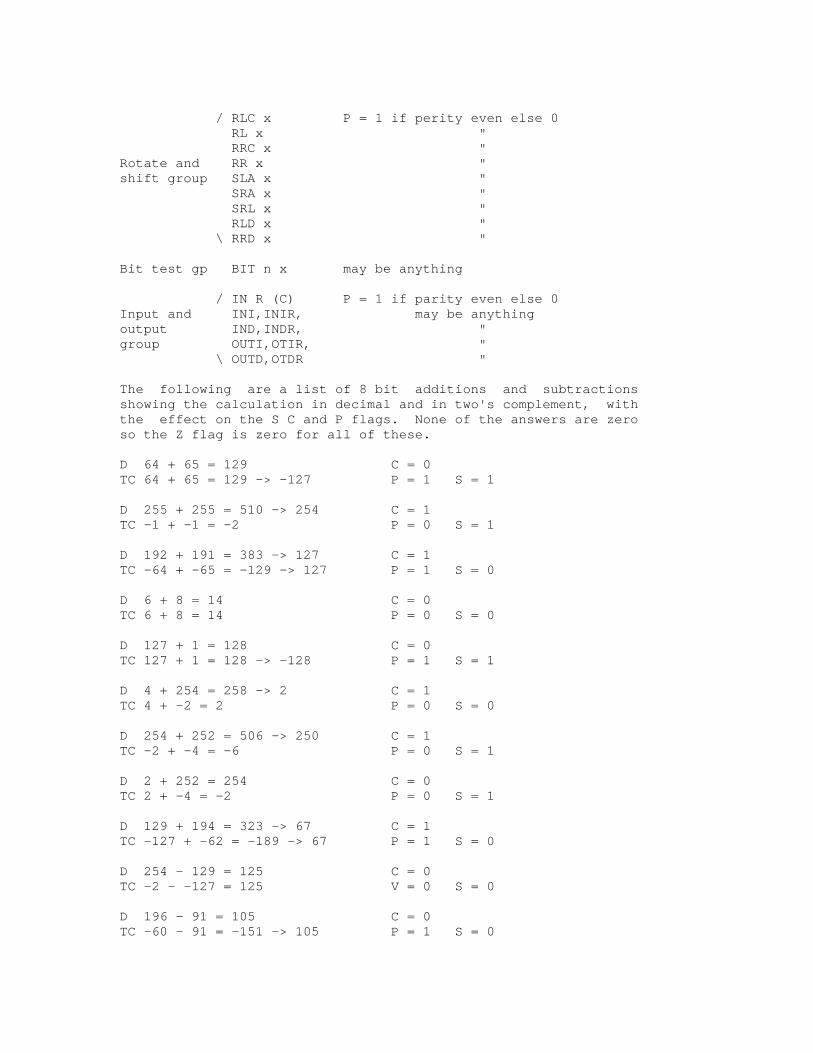
/ RLC x P = 1 if perity even else 0 RL x " RRC x " Rotate and RR x " shift group SLA x " SRA x " SRL x " RLD x " \ RRD x " Bit test gp BIT n x may be anything / IN R (C) P = 1 if parity even else 0 Input and INI,INIR, may be anything output IND,INDR, " group OUTI,OTIR, " \ OUTD,OTDR " The following are a list of 8 bit additions and subtractions showing the calculation in decimal and in two's complement, with the effect on the S C and P flags. None of the answers are zero so the Z flag is zero for all of these. D 64 + 65 = 129 C = 0 TC 64 + 65 = 129 -> -127 P = 1 S = 1 D 255 + 255 = 510 -> 254 C = 1 TC -1 + -1 = -2 P = 0 S = 1 D 192 + 191 = 383 -> 127 C = 1 TC -64 + -65 = -129 -> 127 P = 1 S = 0 D 6 + 8 = 14 C = 0 TC 6 + 8 = 14 P = 0 S = 0 D 127 + 1 = 128 C = 0 TC 127 + 1 = 128 -> -128 P = 1 S = 1 D 4 + 254 = 258 -> 2 C = 1 TC 4 + -2 = 2 P = 0 S = 0 D 254 + 252 = 506 -> 250 C = 1 TC -2 + -4 = -6 P = 0 S = 1 D 2 + 252 = 254 C = 0 TC 2 + -4 = -2 P = 0 S = 1 D 129 + 194 = 323 -> 67 C = 1 TC -127 + -62 = -189 -> 67 P = 1 S = 0 D 254 - 129 = 125 C = 0 TC -2 - -127 = 125 V = 0 S = 0 D 196 - 91 = 105 C = 0 TC -60 - 91 = -151 -> 105 P = 1 S = 0
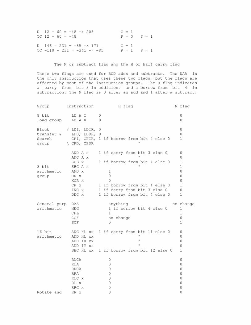
D 12 - 60 = -48 -> 208 C = 1 TC 12 - 60 = -48 P = 0 S = 1 D 146 - 231 = -85 -> 171 C = 1 TC -110 - 231 = -341 -> -85 P = 1 S = 1 The N or subtract flag and the H or half carry flag These two flags are used for BCD adds and subtracts. The DAA is the only instruction that uses these two flags, but the flags are affected by most of the instruction groups. The H flag indicates a carry from bit 3 in addition, and a borrow from bit 4 in subtraction. The N flag is 0 after an add and 1 after a subtract. Group Instruction H flag N flag 8 bit LD A I 0 0 load group LD A R 0 0 Block / LDI, LDIR, 0 0 transfer & LDD, LDDR, 0 0 Search CPI, CPIR, 1 if borrow from bit 4 else 0 1 group \ CPD, CPDR " ADD A x 1 if carry from bit 3 else 0 0 ADC A x " 0 SUB x 1 if borrow from bit 4 else 0 1 8 bit SBC A x " 1 arithmetic AND x 1 0 group OR x 0 0 XOR x 0 0 CP x 1 if borrow from bit 4 else 0 1 INC x 1 if carry from bit 3 else 0 0 DEC x 1 if borrow from bit 4 else 0 1 General purp DAA anything no change arithmetic NEG 1 if borrow bit 4 else 0 1 CPL 1 1 CCF no change 0 SCF 0 1 16 bit ADC HL xx 1 if carry from bit 11 else 0 0 arithmetic ADD HL xx " 0 ADD IX xx " 0 ADD IY xx " 0 SBC HL xx 1 if borrow from bit 12 else 0 1 RLCA 0 0 RLA 0 0 RRCA 0 0 RRA 0 0 RLC x 0 0 RL x 0 0 RRC x 0 0 Rotate and RR x 0 0
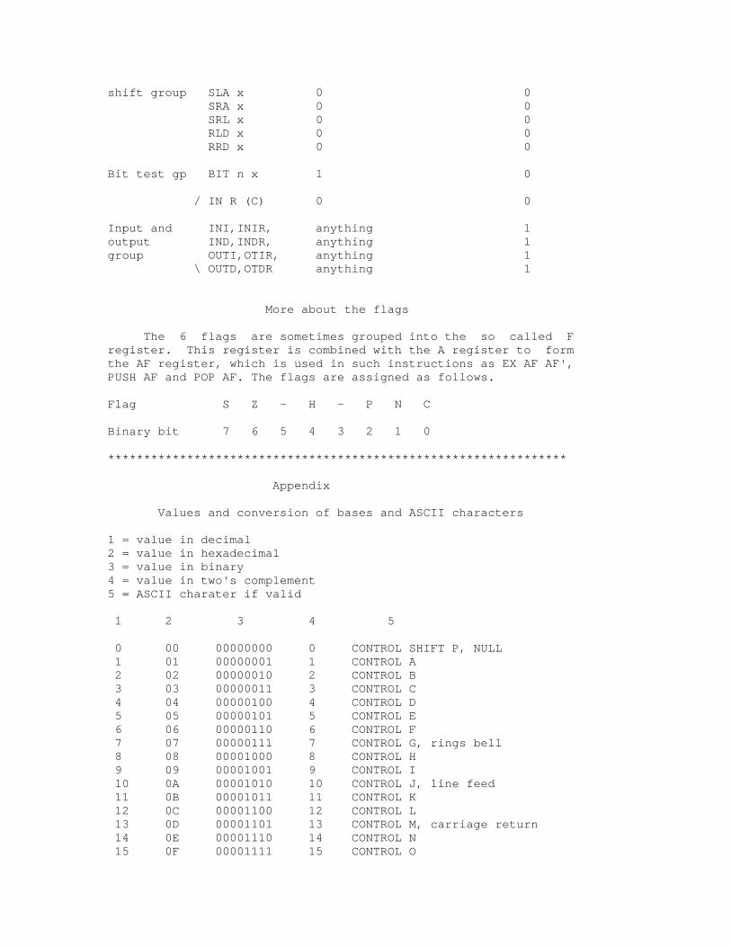
shift group SLA x 0 0 SRA x 0 0 SRL x 0 0 RLD x 0 0 RRD x 0 0 Bit test gp BIT n x 1 0 / IN R (C) 0 0 Input and INI,INIR, anything 1 output IND,INDR, anything 1 group OUTI,OTIR, anything 1 \ OUTD,OTDR anything 1 More about the flags The 6 flags are sometimes grouped into the so called F register. This register is combined with the A register to form the AF register, which is used in such instructions as EX AF AF', PUSH AF and POP AF. The flags are assigned as follows. Flag S Z - H - P N C Binary bit 7 6 5 4 3 2 1 0 **************************************************************** Appendix Values and conversion of bases and ASCII characters 1 = value in decimal 2 = value in hexadecimal 3 = value in binary 4 = value in two's complement 5 = ASCII charater if valid 1 2 3 4 5 0 00 00000000 0 CONTROL SHIFT P, NULL 1 01 00000001 1 CONTROL A 2 02 00000010 2 CONTROL B 3 03 00000011 3 CONTROL C 4 04 00000100 4 CONTROL D 5 05 00000101 5 CONTROL E 6 06 00000110 6 CONTROL F 7 07 00000111 7 CONTROL G, rings bell 8 08 00001000 8 CONTROL H 9 09 00001001 9 CONTROL I 10 0A 00001010 10 CONTROL J, line feed 11 0B 00001011 11 CONTROL K 12 0C 00001100 12 CONTROL L 13 0D 00001101 13 CONTROL M, carriage return 14 0E 00001110 14 CONTROL N 15 0F 00001111 15 CONTROL O
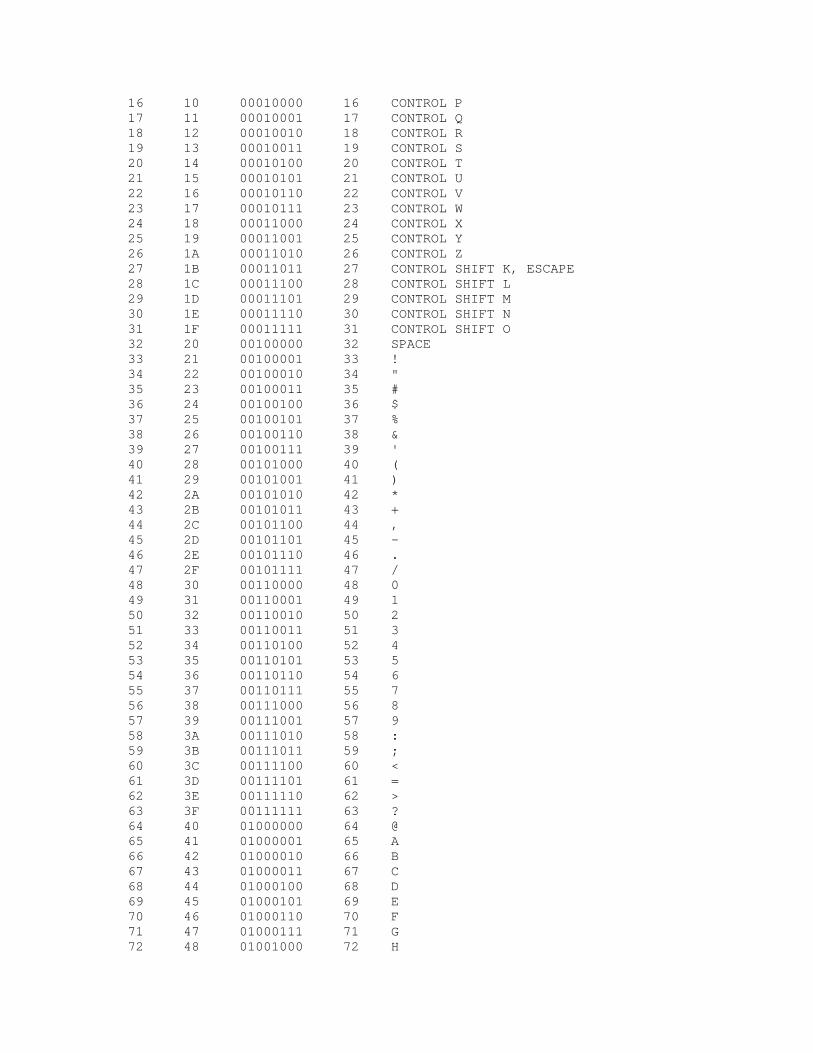
16 10 00010000 16 CONTROL P 17 11 00010001 17 CONTROL Q 18 12 00010010 18 CONTROL R 19 13 00010011 19 CONTROL S 20 14 00010100 20 CONTROL T 21 15 00010101 21 CONTROL U 22 16 00010110 22 CONTROL V 23 17 00010111 23 CONTROL W 24 18 00011000 24 CONTROL X 25 19 00011001 25 CONTROL Y 26 1A 00011010 26 CONTROL Z 27 1B 00011011 27 CONTROL SHIFT K, ESCAPE 28 1C 00011100 28 CONTROL SHIFT L 29 1D 00011101 29 CONTROL SHIFT M 30 1E 00011110 30 CONTROL SHIFT N 31 1F 00011111 31 CONTROL SHIFT O 32 20 00100000 32 SPACE 33 21 00100001 33 ! 34 22 00100010 34 " 35 23 00100011 35 # 36 24 00100100 36 $ 37 25 00100101 37 % 38 26 00100110 38 & 39 27 00100111 39 ' 40 28 00101000 40 ( 41 29 00101001 41 ) 42 2A 00101010 42 * 43 2B 00101011 43 + 44 2C 00101100 44 , 45 2D 00101101 45 - 46 2E 00101110 46 . 47 2F 00101111 47 / 48 30 00110000 48 0 49 31 00110001 49 1 50 32 00110010 50 2 51 33 00110011 51 3 52 34 00110100 52 4 53 35 00110101 53 5 54 36 00110110 54 6 55 37 00110111 55 7 56 38 00111000 56 8 57 39 00111001 57 9 58 3A 00111010 58 : 59 3B 00111011 59 ; 60 3C 00111100 60 < 61 3D 00111101 61 = 62 3E 00111110 62 > 63 3F 00111111 63 ? 64 40 01000000 64 @ 65 41 01000001 65 A 66 42 01000010 66 B 67 43 01000011 67 C 68 44 01000100 68 D 69 45 01000101 69 E 70 46 01000110 70 F 71 47 01000111 71 G 72 48 01001000 72 H
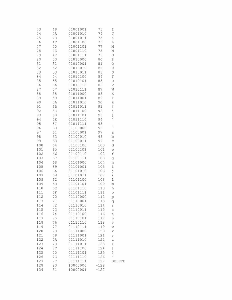
73 49 01001001 73 I 74 4A 01001010 74 J 75 4B 01001011 75 K 76 4C 01001100 76 L 77 4D 01001101 77 M 78 4E 01001110 78 N 79 4F 01001111 79 O 80 50 01010000 80 P 81 51 01010001 81 Q 82 52 01010010 82 R 83 53 01010011 83 S 84 54 01010100 84 T 85 55 01010101 85 U 86 56 01010110 86 V 87 57 01010111 87 W 88 58 01011000 88 X 89 59 01011001 89 Y 90 5A 01011010 90 Z 91 5B 01011011 91 [ 92 5C 01011100 92 \ 93 5D 01011101 93 ] 94 5E 01011110 94 ^ 95 5F 01011111 95 _ 96 60 01100000 96 ` 97 61 01100001 97 a 98 62 01100010 98 b 99 63 01100011 99 c 100 64 01100100 100 d 101 65 01100101 101 e 102 66 01100110 102 f 103 67 01100111 103 g 104 68 01101000 104 h 105 69 01101001 105 i 106 6A 01101010 106 j 107 6B 01101011 107 k 108 6C 01101100 108 l 109 6D 01101101 109 m 110 6E 01101110 110 n 111 6F 01101111 111 o 112 70 01110000 112 p 113 71 01110001 113 q 114 72 01110010 114 r 115 73 01110011 115 s 116 74 01110100 116 t 117 75 01110101 117 u 118 76 01110110 118 v 119 77 01110111 119 w 120 78 01111000 120 x 121 79 01111001 121 y 122 7A 01111010 122 z 123 7B 01111011 123 { 124 7C 01111100 124 | 125 7D 01111101 125 } 126 7E 01111110 126 ~ 127 7F 01111111 127 DELETE 128 80 10000000 -128 129 81 10000001 -127

130 82 10000010 -126 131 83 10000011 -125 132 84 10000100 -124 133 85 10000101 -123 134 86 10000110 -122 135 87 10000111 -121 136 88 10001000 -120 137 89 10001001 -119 138 8A 10001010 -118 139 8B 10001011 -117 140 8C 10001100 -116 141 8D 10001101 -115 142 8E 10001110 -114 143 8F 10001111 -113 144 90 10010000 -112 145 91 10010001 -111 146 92 10010010 -110 147 93 10010011 -109 148 94 10010100 -108 149 95 10010101 -107 150 96 10010110 -106 151 97 10010111 -105 152 98 10011000 -104 153 99 10011001 -103 154 9A 10011010 -102 155 9B 10011011 -101 156 9C 10011100 -100 157 9D 10011101 -99 158 9E 10011110 -98 159 9F 10011111 -97 160 A0 10100000 -96 161 A1 10100001 -95 162 A2 10100010 -94 163 A3 10100011 -93 164 A4 10100100 -92 165 A5 10100101 -91 166 A6 10100110 -90 167 A7 10100111 -89 168 A8 10101000 -88 169 A9 10101001 -87 170 AA 10101010 -86 171 AB 10101011 -85 172 AC 10101100 -84 173 AD 10101101 -83 174 AE 10101110 -82 175 AF 10101111 -81 176 B0 10110000 -80 177 B1 10110001 -79 178 B2 10110010 -78 179 B3 10110011 -77 180 B4 10110100 -76 181 B5 10110101 -75 182 B6 10110110 -74 183 B7 10110111 -73 184 B8 10111000 -72 185 B9 10111001 -71 186 BA 10111010 -70
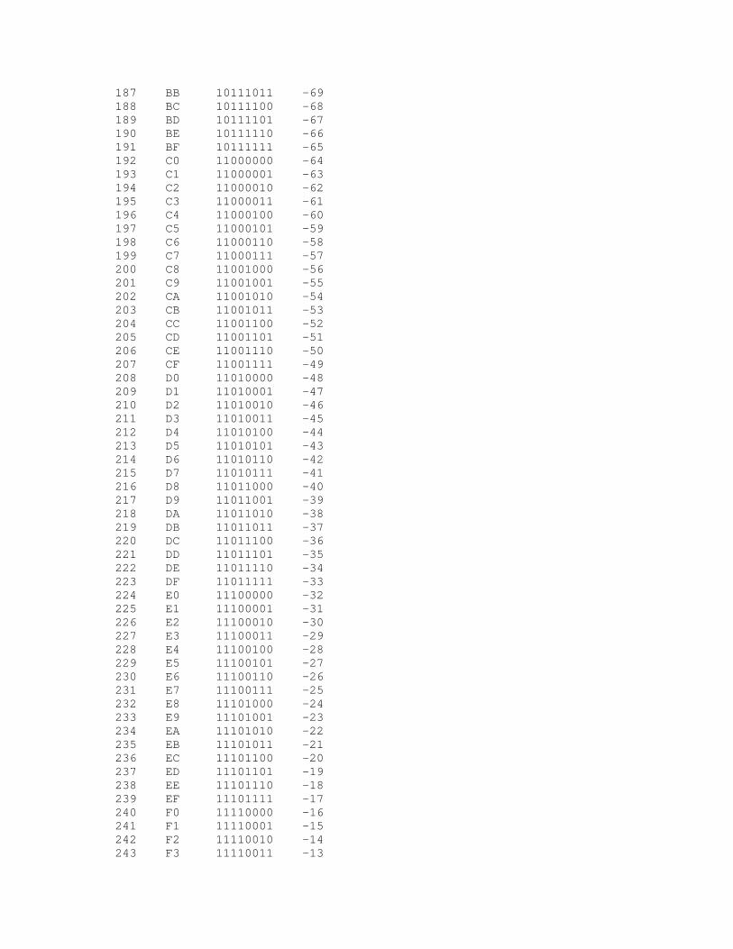
187 BB 10111011 -69 188 BC 10111100 -68 189 BD 10111101 -67 190 BE 10111110 -66 191 BF 10111111 -65 192 C0 11000000 -64 193 C1 11000001 -63 194 C2 11000010 -62 195 C3 11000011 -61 196 C4 11000100 -60 197 C5 11000101 -59 198 C6 11000110 -58 199 C7 11000111 -57 200 C8 11001000 -56 201 C9 11001001 -55 202 CA 11001010 -54 203 CB 11001011 -53 204 CC 11001100 -52 205 CD 11001101 -51 206 CE 11001110 -50 207 CF 11001111 -49 208 D0 11010000 -48 209 D1 11010001 -47 210 D2 11010010 -46 211 D3 11010011 -45 212 D4 11010100 -44 213 D5 11010101 -43 214 D6 11010110 -42 215 D7 11010111 -41 216 D8 11011000 -40 217 D9 11011001 -39 218 DA 11011010 -38 219 DB 11011011 -37 220 DC 11011100 -36 221 DD 11011101 -35 222 DE 11011110 -34 223 DF 11011111 -33 224 E0 11100000 -32 225 E1 11100001 -31 226 E2 11100010 -30 227 E3 11100011 -29 228 E4 11100100 -28 229 E5 11100101 -27 230 E6 11100110 -26 231 E7 11100111 -25 232 E8 11101000 -24 233 E9 11101001 -23 234 EA 11101010 -22 235 EB 11101011 -21 236 EC 11101100 -20 237 ED 11101101 -19 238 EE 11101110 -18 239 EF 11101111 -17 240 F0 11110000 -16 241 F1 11110001 -15 242 F2 11110010 -14 243 F3 11110011 -13
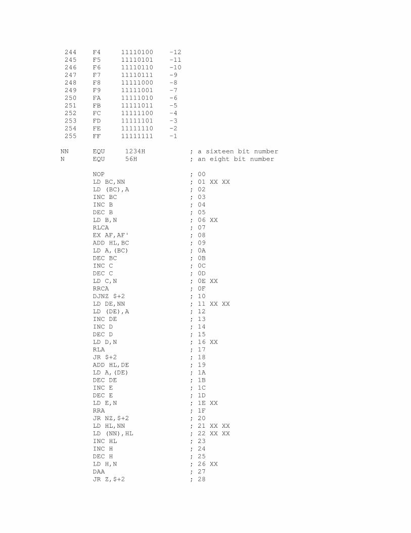
244 F4 11110100 -12 245 F5 11110101 -11 246 F6 11110110 -10 247 F7 11110111 -9 248 F8 11111000 -8 249 F9 11111001 -7 250 FA 11111010 -6 251 FB 11111011 -5 252 FC 11111100 -4 253 FD 11111101 -3 254 FE 11111110 -2 255 FF 11111111 -1 NN EQU 1234H ; a sixteen bit number N EQU 56H ; an eight bit number NOP ; 00 LD BC,NN ; 01 XX XX LD (BC),A ; 02 INC BC ; 03 INC B ; 04 DEC B ; 05 LD B,N ; 06 XX RLCA ; 07 EX AF,AF' ; 08 ADD HL,BC ; 09 LD A,(BC) ; 0A DEC BC ; 0B INC C ; 0C DEC C ; 0D LD C,N ; 0E XX RRCA ; 0F DJNZ $+2 ; 10 LD DE,NN ; 11 XX XX LD (DE),A ; 12 INC DE ; 13 INC D ; 14 DEC D ; 15 LD D,N ; 16 XX RLA ; 17 JR $+2 ; 18 ADD HL,DE ; 19 LD A,(DE) ; 1A DEC DE ; 1B INC E ; 1C DEC E ; 1D LD E,N ; 1E XX RRA ; 1F JR NZ,$+2 ; 20 LD HL,NN ; 21 XX XX LD (NN),HL ; 22 XX XX INC HL ; 23 INC H ; 24 DEC H ; 25 LD H,N ; 26 XX DAA ; 27 JR Z,$+2 ; 28
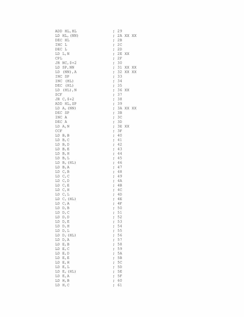
ADD HL,HL ; 29 LD HL,(NN) ; 2A XX XX DEC HL ; 2B INC L ; 2C DEC L ; 2D LD L,N ; 2E XX CPL ; 2F JR NC,$+2 ; 30 LD SP,NN ; 31 XX XX LD (NN),A ; 32 XX XX INC SP ; 33 INC (HL) ; 34 DEC (HL) ; 35 LD (HL),N ; 36 XX SCF ; 37 JR C,$+2 ; 38 ADD HL,SP ; 39 LD A,(NN) ; 3A XX XX DEC SP ; 3B INC A ; 3C DEC A ; 3D LD A,N ; 3E XX CCF ; 3F LD B,B ; 40 LD B,C ; 41 LD B,D ; 42 LD B,E ; 43 LD B,H ; 44 LD B,L ; 45 LD B,(HL) ; 46 LD B,A ; 47 LD C,B ; 48 LD C,C ; 49 LD C,D ; 4A LD C,E ; 4B LD C,H ; 4C LD C,L ; 4D LD C,(HL) ; 4E LD C,A ; 4F LD D,B ; 50 LD D,C ; 51 LD D,D ; 52 LD D,E ; 53 LD D,H ; 54 LD D,L ; 55 LD D,(HL) ; 56 LD D,A ; 57 LD E,B ; 58 LD E,C ; 59 LD E,D ; 5A LD E,E ; 5B LD E,H ; 5C LD E,L ; 5D LD E,(HL) ; 5E LD E,A ; 5F LD H,B ; 60 LD H,C ; 61
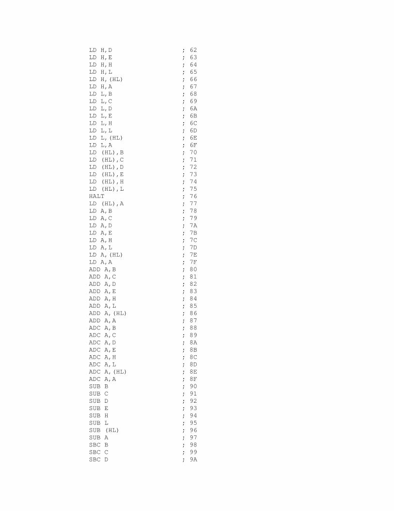
LD H,D ; 62 LD H,E ; 63 LD H,H ; 64 LD H,L ; 65 LD H,(HL) ; 66 LD H,A ; 67 LD L,B ; 68 LD L,C ; 69 LD L,D ; 6A LD L,E ; 6B LD L,H ; 6C LD L,L ; 6D LD L,(HL) ; 6E LD L,A ; 6F LD (HL),B ; 70 LD (HL),C ; 71 LD (HL),D ; 72 LD (HL),E ; 73 LD (HL),H ; 74 LD (HL),L ; 75 HALT ; 76 LD (HL),A ; 77 LD A,B ; 78 LD A,C ; 79 LD A,D ; 7A LD A,E ; 7B LD A,H ; 7C LD A,L ; 7D LD A,(HL) ; 7E LD A,A ; 7F ADD A,B ; 80 ADD A,C ; 81 ADD A,D ; 82 ADD A,E ; 83 ADD A,H ; 84 ADD A,L ; 85 ADD A,(HL) ; 86 ADD A,A ; 87 ADC A,B ; 88 ADC A,C ; 89 ADC A,D ; 8A ADC A,E ; 8B ADC A,H ; 8C ADC A,L ; 8D ADC A,(HL) ; 8E ADC A,A ; 8F SUB B ; 90 SUB C ; 91 SUB D ; 92 SUB E ; 93 SUB H ; 94 SUB L ; 95 SUB (HL) ; 96 SUB A ; 97 SBC B ; 98 SBC C ; 99 SBC D ; 9A
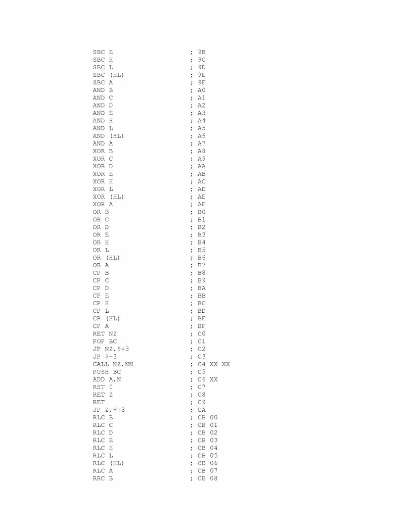
SBC E ; 9B SBC H ; 9C SBC L ; 9D SBC (HL) ; 9E SBC A ; 9F AND B ; A0 AND C ; A1 AND D ; A2 AND E ; A3 AND H ; A4 AND L ; A5 AND (HL) ; A6 AND A ; A7 XOR B ; A8 XOR C ; A9 XOR D ; AA XOR E ; AB XOR H ; AC XOR L ; AD XOR (HL) ; AE XOR A ; AF OR B ; B0 OR C ; B1 OR D ; B2 OR E ; B3 OR H ; B4 OR L ; B5 OR (HL) ; B6 OR A ; B7 CP B ; B8 CP C ; B9 CP D ; BA CP E ; BB CP H ; BC CP L ; BD CP (HL) ; BE CP A ; BF RET NZ ; C0 POP BC ; C1 JP NZ,$+3 ; C2 JP $+3 ; C3 CALL NZ,NN ; C4 XX XX PUSH BC ; C5 ADD A,N ; C6 XX RST 0 ; C7 RET Z ; C8 RET ; C9 JP Z,$+3 ; CA RLC B ; CB 00 RLC C ; CB 01 RLC D ; CB 02 RLC E ; CB 03 RLC H ; CB 04 RLC L ; CB 05 RLC (HL) ; CB 06 RLC A ; CB 07 RRC B ; CB 08
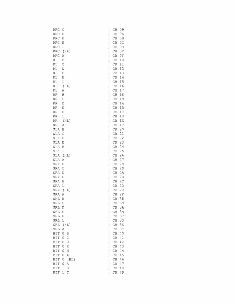
RRC C ; CB 09 RRC D ; CB 0A RRC E ; CB 0B RRC H ; CB 0C RRC L ; CB 0D RRC (HL) ; CB 0E RRC A ; CB 0F RL B ; CB 10 RL C ; CB 11 RL D ; CB 12 RL E ; CB 13 RL H ; CB 14 RL L ; CB 15 RL (HL) ; CB 16 RL A ; CB 17 RR B ; CB 18 RR C ; CB 19 RR D ; CB 1A RR E ; CB 1B RR H ; CB 1C RR L ; CB 1D RR (HL) ; CB 1E RR A ; CB 1F SLA B ; CB 20 SLA C ; CB 21 SLA D ; CB 22 SLA E ; CB 23 SLA H ; CB 24 SLA L ; CB 25 SLA (HL) ; CB 26 SLA A ; CB 27 SRA B ; CB 28 SRA C ; CB 29 SRA D ; CB 2A SRA E ; CB 2B SRA H ; CB 2C SRA L ; CB 2D SRA (HL) ; CB 2E SRA A ; CB 2F SRL B ; CB 38 SRL C ; CB 39 SRL D ; CB 3A SRL E ; CB 3B SRL H ; CB 3C SRL L ; CB 3D SRL (HL) ; CB 3E SRL A ; CB 3F BIT 0,B ; CB 40 BIT 0,C ; CB 41 BIT 0,D ; CB 42 BIT 0,E ; CB 43 BIT 0,H ; CB 44 BIT 0,L ; CB 45 BIT 0,(HL) ; CB 46 BIT 0,A ; CB 47 BIT 1,B ; CB 48 BIT 1,C ; CB 49
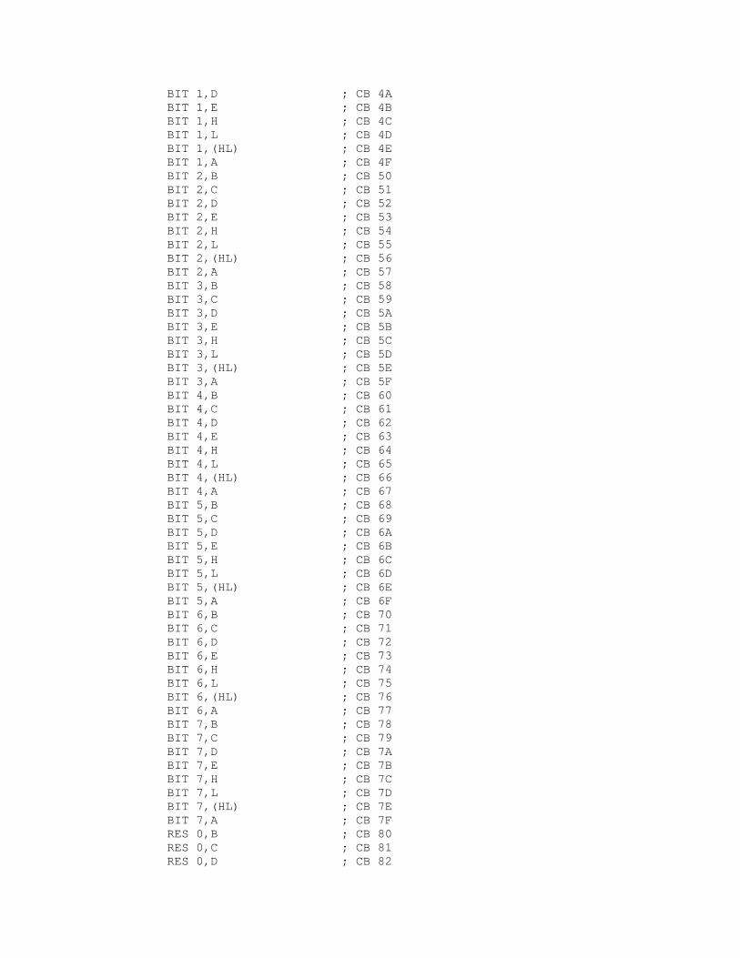
BIT 1,D ; CB 4A BIT 1,E ; CB 4B BIT 1,H ; CB 4C BIT 1,L ; CB 4D BIT 1,(HL) ; CB 4E BIT 1,A ; CB 4F BIT 2,B ; CB 50 BIT 2,C ; CB 51 BIT 2,D ; CB 52 BIT 2,E ; CB 53 BIT 2,H ; CB 54 BIT 2,L ; CB 55 BIT 2,(HL) ; CB 56 BIT 2,A ; CB 57 BIT 3,B ; CB 58 BIT 3,C ; CB 59 BIT 3,D ; CB 5A BIT 3,E ; CB 5B BIT 3,H ; CB 5C BIT 3,L ; CB 5D BIT 3,(HL) ; CB 5E BIT 3,A ; CB 5F BIT 4,B ; CB 60 BIT 4,C ; CB 61 BIT 4,D ; CB 62 BIT 4,E ; CB 63 BIT 4,H ; CB 64 BIT 4,L ; CB 65 BIT 4,(HL) ; CB 66 BIT 4,A ; CB 67 BIT 5,B ; CB 68 BIT 5,C ; CB 69 BIT 5,D ; CB 6A BIT 5,E ; CB 6B BIT 5,H ; CB 6C BIT 5,L ; CB 6D BIT 5,(HL) ; CB 6E BIT 5,A ; CB 6F BIT 6,B ; CB 70 BIT 6,C ; CB 71 BIT 6,D ; CB 72 BIT 6,E ; CB 73 BIT 6,H ; CB 74 BIT 6,L ; CB 75 BIT 6,(HL) ; CB 76 BIT 6,A ; CB 77 BIT 7,B ; CB 78 BIT 7,C ; CB 79 BIT 7,D ; CB 7A BIT 7,E ; CB 7B BIT 7,H ; CB 7C BIT 7,L ; CB 7D BIT 7,(HL) ; CB 7E BIT 7,A ; CB 7F RES 0,B ; CB 80 RES 0,C ; CB 81 RES 0,D ; CB 82
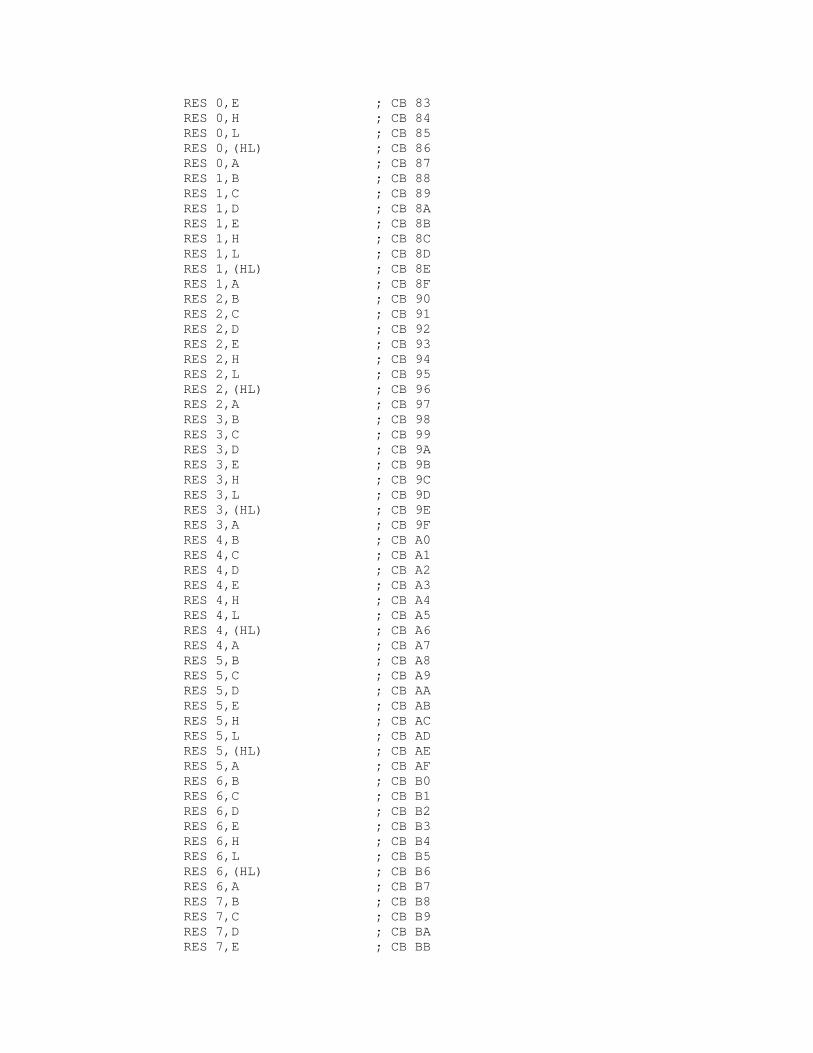
RES 0,E ; CB 83 RES 0,H ; CB 84 RES 0,L ; CB 85 RES 0,(HL) ; CB 86 RES 0,A ; CB 87 RES 1,B ; CB 88 RES 1,C ; CB 89 RES 1,D ; CB 8A RES 1,E ; CB 8B RES 1,H ; CB 8C RES 1,L ; CB 8D RES 1,(HL) ; CB 8E RES 1,A ; CB 8F RES 2,B ; CB 90 RES 2,C ; CB 91 RES 2,D ; CB 92 RES 2,E ; CB 93 RES 2,H ; CB 94 RES 2,L ; CB 95 RES 2,(HL) ; CB 96 RES 2,A ; CB 97 RES 3,B ; CB 98 RES 3,C ; CB 99 RES 3,D ; CB 9A RES 3,E ; CB 9B RES 3,H ; CB 9C RES 3,L ; CB 9D RES 3,(HL) ; CB 9E RES 3,A ; CB 9F RES 4,B ; CB A0 RES 4,C ; CB A1 RES 4,D ; CB A2 RES 4,E ; CB A3 RES 4,H ; CB A4 RES 4,L ; CB A5 RES 4,(HL) ; CB A6 RES 4,A ; CB A7 RES 5,B ; CB A8 RES 5,C ; CB A9 RES 5,D ; CB AA RES 5,E ; CB AB RES 5,H ; CB AC RES 5,L ; CB AD RES 5,(HL) ; CB AE RES 5,A ; CB AF RES 6,B ; CB B0 RES 6,C ; CB B1 RES 6,D ; CB B2 RES 6,E ; CB B3 RES 6,H ; CB B4 RES 6,L ; CB B5 RES 6,(HL) ; CB B6 RES 6,A ; CB B7 RES 7,B ; CB B8 RES 7,C ; CB B9 RES 7,D ; CB BA RES 7,E ; CB BB
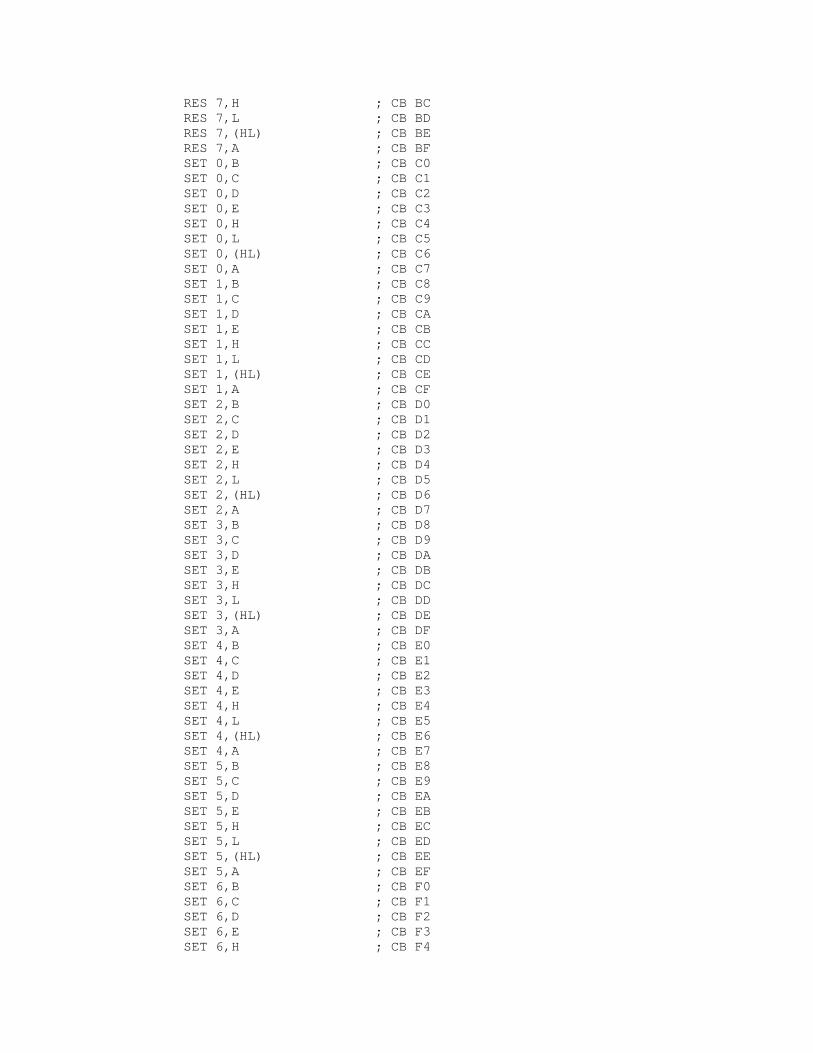
RES 7,H ; CB BC RES 7,L ; CB BD RES 7,(HL) ; CB BE RES 7,A ; CB BF SET 0,B ; CB C0 SET 0,C ; CB C1 SET 0,D ; CB C2 SET 0,E ; CB C3 SET 0,H ; CB C4 SET 0,L ; CB C5 SET 0,(HL) ; CB C6 SET 0,A ; CB C7 SET 1,B ; CB C8 SET 1,C ; CB C9 SET 1,D ; CB CA SET 1,E ; CB CB SET 1,H ; CB CC SET 1,L ; CB CD SET 1,(HL) ; CB CE SET 1,A ; CB CF SET 2,B ; CB D0 SET 2,C ; CB D1 SET 2,D ; CB D2 SET 2,E ; CB D3 SET 2,H ; CB D4 SET 2,L ; CB D5 SET 2,(HL) ; CB D6 SET 2,A ; CB D7 SET 3,B ; CB D8 SET 3,C ; CB D9 SET 3,D ; CB DA SET 3,E ; CB DB SET 3,H ; CB DC SET 3,L ; CB DD SET 3,(HL) ; CB DE SET 3,A ; CB DF SET 4,B ; CB E0 SET 4,C ; CB E1 SET 4,D ; CB E2 SET 4,E ; CB E3 SET 4,H ; CB E4 SET 4,L ; CB E5 SET 4,(HL) ; CB E6 SET 4,A ; CB E7 SET 5,B ; CB E8 SET 5,C ; CB E9 SET 5,D ; CB EA SET 5,E ; CB EB SET 5,H ; CB EC SET 5,L ; CB ED SET 5,(HL) ; CB EE SET 5,A ; CB EF SET 6,B ; CB F0 SET 6,C ; CB F1 SET 6,D ; CB F2 SET 6,E ; CB F3 SET 6,H ; CB F4
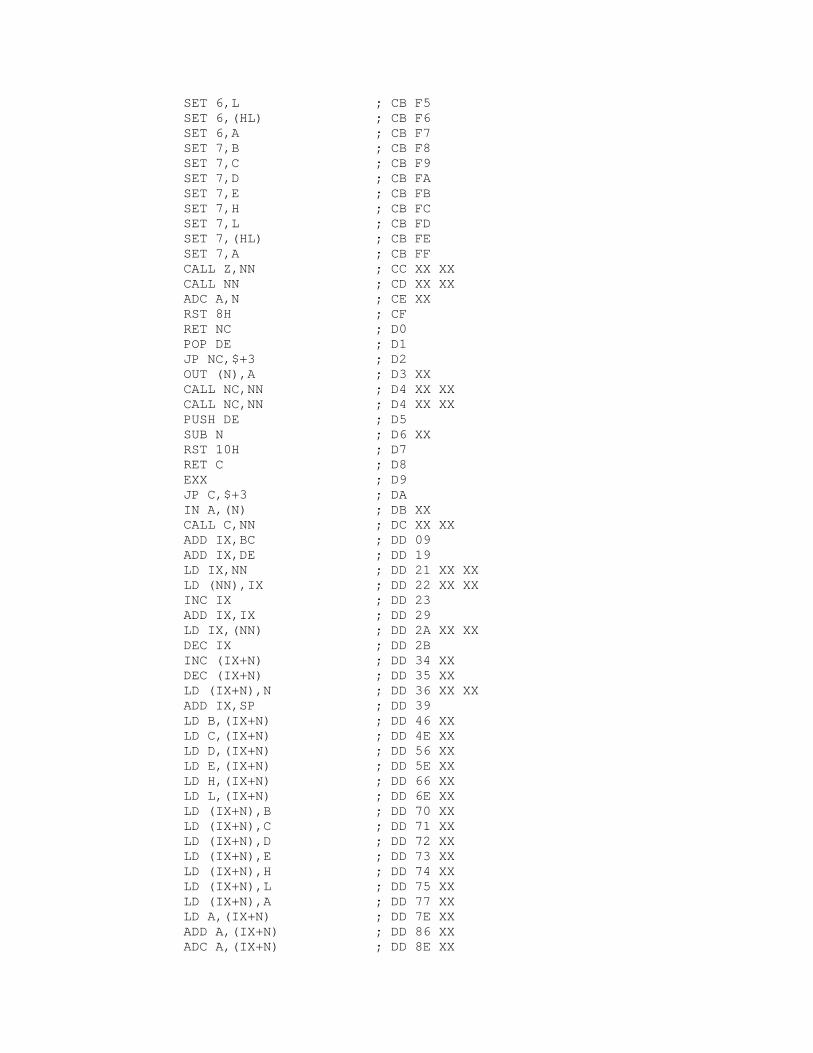
SET 6,L ; CB F5 SET 6,(HL) ; CB F6 SET 6,A ; CB F7 SET 7,B ; CB F8 SET 7,C ; CB F9 SET 7,D ; CB FA SET 7,E ; CB FB SET 7,H ; CB FC SET 7,L ; CB FD SET 7,(HL) ; CB FE SET 7,A ; CB FF CALL Z,NN ; CC XX XX CALL NN ; CD XX XX ADC A,N ; CE XX RST 8H ; CF RET NC ; D0 POP DE ; D1 JP NC,$+3 ; D2 OUT (N),A ; D3 XX CALL NC,NN ; D4 XX XX CALL NC,NN ; D4 XX XX PUSH DE ; D5 SUB N ; D6 XX RST 10H ; D7 RET C ; D8 EXX ; D9 JP C,$+3 ; DA IN A,(N) ; DB XX CALL C,NN ; DC XX XX ADD IX,BC ; DD 09 ADD IX,DE ; DD 19 LD IX,NN ; DD 21 XX XX LD (NN),IX ; DD 22 XX XX INC IX ; DD 23 ADD IX,IX ; DD 29 LD IX,(NN) ; DD 2A XX XX DEC IX ; DD 2B INC (IX+N) ; DD 34 XX DEC (IX+N) ; DD 35 XX LD (IX+N),N ; DD 36 XX XX ADD IX,SP ; DD 39 LD B,(IX+N) ; DD 46 XX LD C,(IX+N) ; DD 4E XX LD D,(IX+N) ; DD 56 XX LD E,(IX+N) ; DD 5E XX LD H,(IX+N) ; DD 66 XX LD L,(IX+N) ; DD 6E XX LD (IX+N),B ; DD 70 XX LD (IX+N),C ; DD 71 XX LD (IX+N),D ; DD 72 XX LD (IX+N),E ; DD 73 XX LD (IX+N),H ; DD 74 XX LD (IX+N),L ; DD 75 XX LD (IX+N),A ; DD 77 XX LD A,(IX+N) ; DD 7E XX ADD A,(IX+N) ; DD 86 XX ADC A,(IX+N) ; DD 8E XX
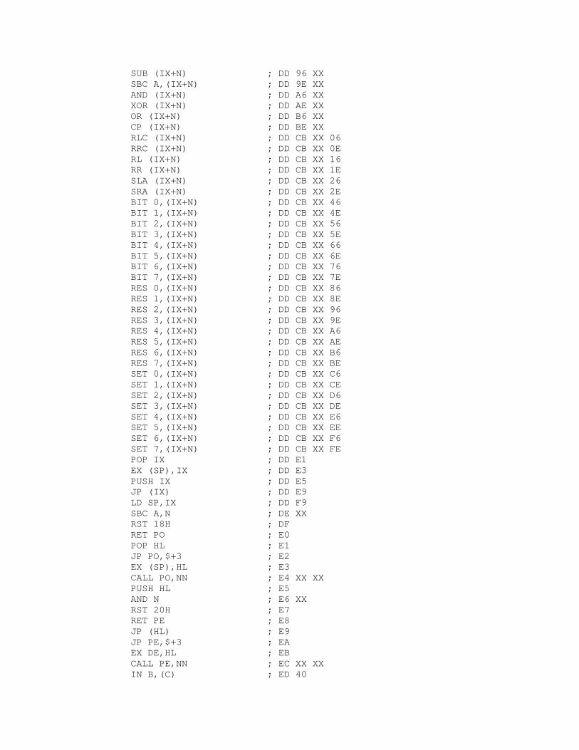
SUB (IX+N) ; DD 96 XX SBC A,(IX+N) ; DD 9E XX AND (IX+N) ; DD A6 XX XOR (IX+N) ; DD AE XX OR (IX+N) ; DD B6 XX CP (IX+N) ; DD BE XX RLC (IX+N) ; DD CB XX 06 RRC (IX+N) ; DD CB XX 0E RL (IX+N) ; DD CB XX 16 RR (IX+N) ; DD CB XX 1E SLA (IX+N) ; DD CB XX 26 SRA (IX+N) ; DD CB XX 2E BIT 0,(IX+N) ; DD CB XX 46 BIT 1,(IX+N) ; DD CB XX 4E BIT 2,(IX+N) ; DD CB XX 56 BIT 3,(IX+N) ; DD CB XX 5E BIT 4,(IX+N) ; DD CB XX 66 BIT 5,(IX+N) ; DD CB XX 6E BIT 6,(IX+N) ; DD CB XX 76 BIT 7,(IX+N) ; DD CB XX 7E RES 0,(IX+N) ; DD CB XX 86 RES 1,(IX+N) ; DD CB XX 8E RES 2,(IX+N) ; DD CB XX 96 RES 3,(IX+N) ; DD CB XX 9E RES 4,(IX+N) ; DD CB XX A6 RES 5,(IX+N) ; DD CB XX AE RES 6,(IX+N) ; DD CB XX B6 RES 7,(IX+N) ; DD CB XX BE SET 0,(IX+N) ; DD CB XX C6 SET 1,(IX+N) ; DD CB XX CE SET 2,(IX+N) ; DD CB XX D6 SET 3,(IX+N) ; DD CB XX DE SET 4,(IX+N) ; DD CB XX E6 SET 5,(IX+N) ; DD CB XX EE SET 6,(IX+N) ; DD CB XX F6 SET 7,(IX+N) ; DD CB XX FE POP IX ; DD E1 EX (SP),IX ; DD E3 PUSH IX ; DD E5 JP (IX) ; DD E9 LD SP,IX ; DD F9 SBC A,N ; DE XX RST 18H ; DF RET PO ; E0 POP HL ; E1 JP PO,$+3 ; E2 EX (SP),HL ; E3 CALL PO,NN ; E4 XX XX PUSH HL ; E5 AND N ; E6 XX RST 20H ; E7 RET PE ; E8 JP (HL) ; E9 JP PE,$+3 ; EA EX DE,HL ; EB CALL PE,NN ; EC XX XX IN B,(C) ; ED 40
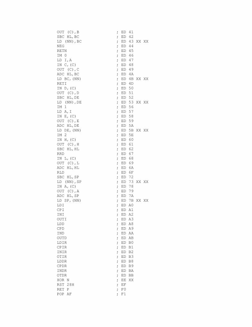
OUT (C),B ; ED 41 SBC HL,BC ; ED 42 LD (NN),BC ; ED 43 XX XX NEG ; ED 44 RETN ; ED 45 IM 0 ; ED 46 LD I,A ; ED 47 IN C,(C) ; ED 48 OUT (C),C ; ED 49 ADC HL,BC ; ED 4A LD BC,(NN) ; ED 4B XX XX RETI ; ED 4D IN D,(C) ; ED 50 OUT (C),D ; ED 51 SBC HL,DE ; ED 52 LD (NN),DE ; ED 53 XX XX IM 1 ; ED 56 LD A,I ; ED 57 IN E,(C) ; ED 58 OUT (C),E ; ED 59 ADC HL,DE ; ED 5A LD DE,(NN) ; ED 5B XX XX IM 2 ; ED 5E IN H,(C) ; ED 60 OUT (C),H ; ED 61 SBC HL,HL ; ED 62 RRD ; ED 67 IN L,(C) ; ED 68 OUT (C),L ; ED 69 ADC HL,HL ; ED 6A RLD ; ED 6F SBC HL,SP ; ED 72 LD (NN),SP ; ED 73 XX XX IN A,(C) ; ED 78 OUT (C),A ; ED 79 ADC HL,SP ; ED 7A LD SP,(NN) ; ED 7B XX XX LDI ; ED A0 CPI ; ED A1 INI ; ED A2 OUTI ; ED A3 LDD ; ED A8 CPD ; ED A9 IND ; ED AA OUTD ; ED AB LDIR ; ED B0 CPIR ; ED B1 INIR ; ED B2 OTIR ; ED B3 LDDR ; ED B8 CPDR ; ED B9 INDR ; ED BA OTDR ; ED BB XOR N ; EE XX RST 28H ; EF RET P ; F0 POP AF ; F1
JP P,$+3 ; F2 DI ; F3 CALL P,NN ; F4 XX XX PUSH AF ; F5 OR N ; F6 XX RST 30H ; F7 RET M ; F8 LD SP,HL ; F9 JP M,$+3 ; FA EI ; FB CALL M,NN ; FC XX XX ADD IY,BC ; FD 09 ADD IY,DE ; FD 19 LD IY,NN ; FD 21 XX XX LD (NN),IY ; FD 22 XX XX INC IY ; FD 23 ADD IY,IY ; FD 29 LD IY,(NN) ; FD 2A XX XX DEC IY ; FD 2B INC (IY+N) ; FD 34 XX DEC (IY+N) ; FD 35 XX LD (IY+N),N ; FD 36 XX XX ADD IY,SP ; FD 39 LD B,(IY+N) ; FD 46 XX LD C,(IY+N) ; FD 4E XX LD D,(IY+N) ; FD 56 XX LD E,(IY+N) ; FD 5E XX LD H,(IY+N) ; FD 66 XX LD L,(IY+N) ; FD 6E XX LD (IY+N),B ; FD 70 XX LD (IY+N),C ; FD 71 XX LD (IY+N),D ; FD 72 XX LD (IY+N),E ; FD 73 XX LD (IY+N),H ; FD 74 XX LD (IY+N),L ; FD 75 XX LD (IY+N),A ; FD 77 XX LD A,(IY+N) ; FD 7E XX ADD A,(IY+N) ; FD 86 XX ADC A,(IY+N) ; FD 8E XX SUB (IY+N) ; FD 96 XX SBC A,(IY+N) ; FD 9E XX AND (IY+N) ; FD A6 XX XOR (IY+N) ; FD AE XX OR (IY+N) ; FD B6 XX CP (IY+N) ; FD BE XX RLC (IY+N) ; FD CB XX 06 RRC (IY+N) ; FD CB XX 0E RL (IY+N) ; FD CB XX 16 RR (IY+N) ; FD CB XX 1E SLA (IY+N) ; FD CB XX 26 SRA (IY+N) ; FD CB XX 2E BIT 0,(IY+N) ; FD CB XX 46 BIT 1,(IY+N) ; FD CB XX 4E BIT 2,(IY+N) ; FD CB XX 56 BIT 3,(IY+N) ; FD CB XX 5E BIT 4,(IY+N) ; FD CB XX 66 BIT 5,(IY+N) ; FD CB XX 6E
BIT 6,(IY+N) ; FD CB XX 76 BIT 7,(IY+N) ; FD CB XX 7E RES 0,(IY+N) ; FD CB XX 86 RES 1,(IY+N) ; FD CB XX 8E RES 2,(IY+N) ; FD CB XX 96 RES 3,(IY+N) ; FD CB XX 9E RES 4,(IY+N) ; FD CB XX A6 RES 5,(IY+N) ; FD CB XX AE RES 6,(IY+N) ; FD CB XX B6 RES 7,(IY+N) ; FD CB XX BE SET 0,(IY+N) ; FD CB XX C6 SET 1,(IY+N) ; FD CB XX CE SET 2,(IY+N) ; FD CB XX D6 SET 3,(IY+N) ; FD CB XX DE SET 4,(IY+N) ; FD CB XX E6 SET 5,(IY+N) ; FD CB XX EE SET 6,(IY+N) ; FD CB XX F6 SET 7,(IY+N) ; FD CB XX FE POP IY ; FD E1 EX (SP),IY ; FD E3 PUSH IY ; FD E5 JP (IY) ; FD E9 LD SP,IY ; FD F9 CP N ; FE XX RST 38H ; FF