the nanostructures group department of solid state physics
TRANSCRIPT
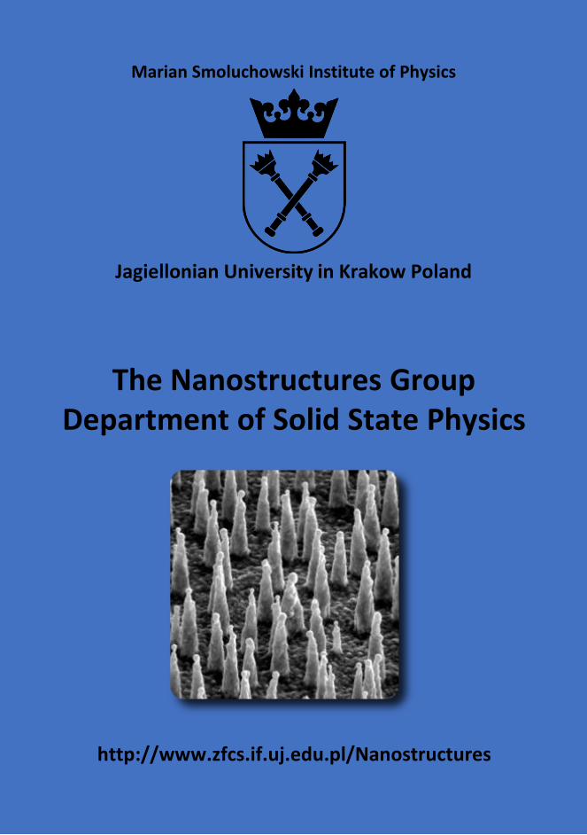
Marian Smoluchowski Institute of Physics
Jagiellonian University in Krakow Poland
The Nanostructures GroupDepartment of Solid State Physics
http://www.zfcs.if.uj.edu.pl/Nanostructures
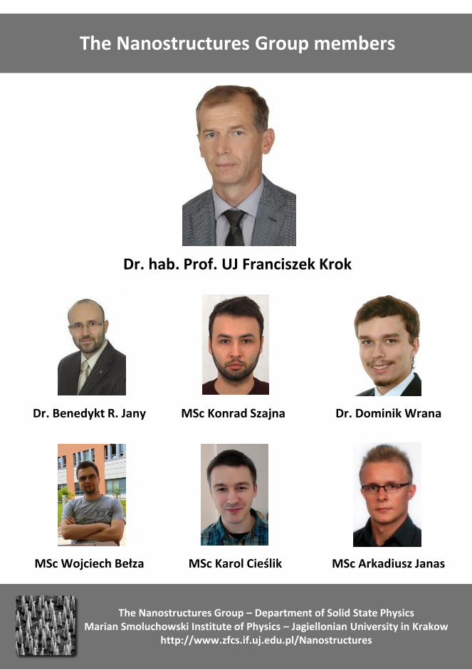
The Nanostructures Group members
Dr. hab. Prof. UJ Franciszek Krok
Dr. Benedykt R. Jany MSc Konrad Szajna Dr. Dominik Wrana
MSc Wojciech Bełza MSc Karol Cieślik MSc Arkadiusz Janas
The Nanostructures Group – Department of Solid State PhysicsMarian Smoluchowski Institute of Physics – Jagiellonian University in Krakow
http://www.zfcs.if.uj.edu.pl/Nanostructures
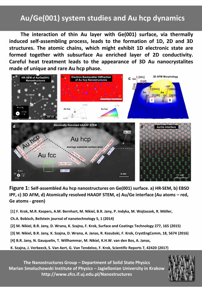
The interaction of thin Au layer with Ge(001) surface, via thermallyinduced self-assembling process, leads to the formation of 1D, 2D and 3Dstructures. The atomic chains, which might exhibit 1D electronic state areformed together with subsurface Au enriched layer of 2D conductivity.Careful heat treatment leads to the appearance of 3D Au nanocrystalitesmade of unique and rare Au hcp phase.
[1] F. Krok, M.R. Kaspers, A.M. Bernhart, M. Nikiel, B.R. Jany, P. Indyka, M. Wojtaszek, R. Möller,
Ch.A. Bobisch, Beilstein journal of nanotechnology 5, 1 (2014)
[2] M. Nikiel, B.R. Jany, D. Wrana, K. Szajna, F. Krok, Surface and Coatings Technology 277, 165 (2015)
[3] M. Nikiel, B.R. Jany, K. Szajna, D. Wrana, A. Janas, R. Kozubski, F. Krok, CrystEngComm, 18, 5674 (2016)
[4] B.R. Jany, N. Gauquelin, T. Willhammar, M. Nikiel, K.H.W. van den Bos, A. Janas,
K. Szajna, J. Verbeeck, S. Van Aert, G. Van Tendeloo, F. Krok, Scientific Reports 7, 42420 (2017)
Au/Ge(001) system studies and Au hcp dynamics
Figure 1: Self-assembled Au hcp nanostructures on Ge(001) surface. a) HR-SEM, b) EBSD
IPF, c) 3D AFM, d) Atomically resolved HAADF STEM, e) Au/Ge interface (Au atoms – red,
Ge atoms - green)
The Nanostructures Group – Department of Solid State PhysicsMarian Smoluchowski Institute of Physics – Jagiellonian University in Krakow
http://www.zfcs.if.uj.edu.pl/Nanostructures

SrTiO3: nanowires formation and redox reactions
The Nanostructures Group – Department of Solid State PhysicsMarian Smoluchowski Institute of Physics – Jagiellonian University in Krakow
http://www.zfcs.if.uj.edu.pl/Nanostructures
Strontium titanate serves as a prototypical material for variousnanotechnology applications. SrTiO3 is a model band insulator, however itselectronic properties can be easily controlled via doping or reduction. Whenthe crystal is heated up, oxygen vacancies are formed but also diffusion ofstrontium and titanium are initiated. When a threshold temperature isreached, micrometers long nanowires of crystalline titanium oxide phases areformed on the surface. They are well oriented and metallic. Upon the crystal’soxidation, surface becomes insulating, yet nanowires are still conducting.Thus, surface redox reactions, diffusion and growth processes on SrTiO3 resultin array of nanoscale conductive 1D structures, which may be used as a wiringfor optoelectronic applications.
Figures: Left: SEM secondary electrons image of the titanium oxide nanowires array on the surface of
the reduced SrTiO3(100).
Right: Atomically resolved HAADF STEM image of the nanowire cross-section. It is clearly
visible that the nanowire is made of pure TiO cubic phase. In the insert detailed view on the
nanowires/substrate zig-zag interface.
D. Wrana, Ch. Rodenbücher, B.R. Jany, A.P. Kryshtal, G. Cempura, A. Kruk, P. Indyka, K. Szot and F. Krok, Bottom-up process of self-formation of highly conductive titanium oxide (TiO) nanowires on reduced SrTiO3, Nanoscale 11, 89-97 (2019)
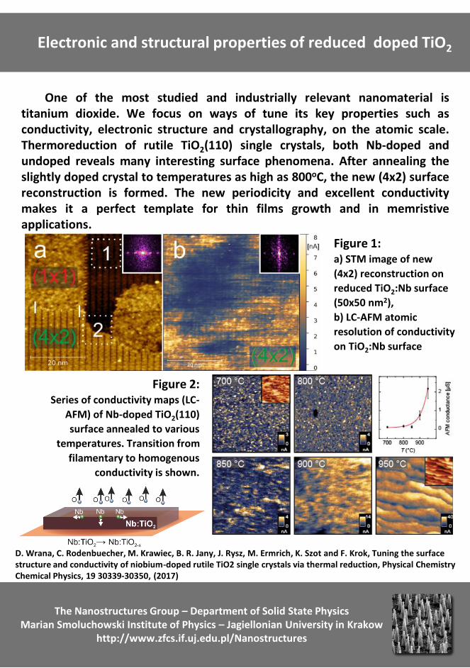
One of the most studied and industrially relevant nanomaterial istitanium dioxide. We focus on ways of tune its key properties such asconductivity, electronic structure and crystallography, on the atomic scale.Thermoreduction of rutile TiO2(110) single crystals, both Nb-doped andundoped reveals many interesting surface phenomena. After annealing theslightly doped crystal to temperatures as high as 800oC, the new (4x2) surfacereconstruction is formed. The new periodicity and excellent conductivitymakes it a perfect template for thin films growth and in memristiveapplications.
Electronic and structural properties of reduced doped TiO2
Figure 1: a) STM image of new
(4x2) reconstruction on
reduced TiO2:Nb surface
(50x50 nm2),
b) LC-AFM atomic
resolution of conductivity
on TiO2:Nb surface
Figure 2: Series of conductivity maps (LC-
AFM) of Nb-doped TiO2(110)
surface annealed to various
temperatures. Transition from
filamentary to homogenous
conductivity is shown.
The Nanostructures Group – Department of Solid State PhysicsMarian Smoluchowski Institute of Physics – Jagiellonian University in Krakow
http://www.zfcs.if.uj.edu.pl/Nanostructures
D. Wrana, C. Rodenbuecher, M. Krawiec, B. R. Jany, J. Rysz, M. Ermrich, K. Szot and F. Krok, Tuning the surface structure and conductivity of niobium-doped rutile TiO2 single crystals via thermal reduction, Physical Chemistry Chemical Physics, 19 30339-30350, (2017)

Titanium dioxide (110) surface preparation & modification
Experiments in the field of surface science usually require an atomically flatand clean surface which can be obtained e.g. for TiO2(110) by subsequentcycles of ion beam sputtering and annealing. However, a highly anisotropicsemiconducting substrate can be also needed. By exposing in particularconditions a TiO2(110) surface to enough high fluence it is possible toproduce in a controllable way a well-defined ripples structure consisting ofdensely packed atomic steps with high crystallographic order.
[1] M. Kratzer, D. Wrana, K. Szajna, F. Krok, and C. Teichert, Phys. Chem. Chem. Phys. 16 (2014)
[2] K. Szajna, M. Kratzer, D. Wrana, C. Mennucci, B. R. Jany, F. Buatier de Mongeot, C. Teichert and F. Krok,
J. Chem. Phys. 145, 144703 (2016)
Figure 1: a) STM image of
atomically flat TiO2(110)
surface with selected
profile,
b) atomic resolution STM
of TiO2(110) surface with
selected profile and LEED
image inset.
Figure 2:STM images of rippled
TiO2(110) surface with:a) shallow ripples that are
parallel to TiO2(110) atomic rows with selected profile,
b) deep ripples that are perpendicular to TiO2(100) atomic rows with selected
profile.
a) b)
a) b)
The Nanostructures Group – Department of Solid State PhysicsMarian Smoluchowski Institute of Physics – Jagiellonian University in Krakow
http://www.zfcs.if.uj.edu.pl/Nanostructures
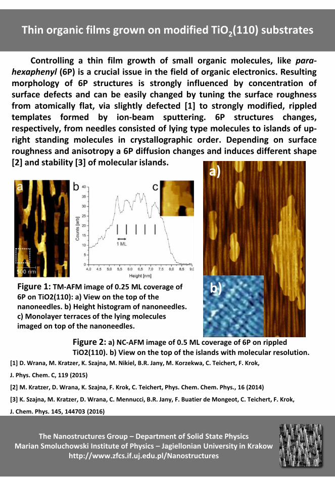
Controlling a thin film growth of small organic molecules, like para-hexaphenyl (6P) is a crucial issue in the field of organic electronics. Resultingmorphology of 6P structures is strongly influenced by concentration ofsurface defects and can be easily changed by tuning the surface roughnessfrom atomically flat, via slightly defected [1] to strongly modified, rippledtemplates formed by ion-beam sputtering. 6P structures changes,respectively, from needles consisted of lying type molecules to islands of up-right standing molecules in crystallographic order. Depending on surfaceroughness and anisotropy a 6P diffusion changes and induces different shape[2] and stability [3] of molecular islands.
Thin organic films grown on modified TiO2(110) substrates
[1] D. Wrana, M. Kratzer, K. Szajna, M. Nikiel, B.R. Jany, M. Korzekwa, C. Teichert, F. Krok,
J. Phys. Chem. C, 119 (2015)
[2] M. Kratzer, D. Wrana, K. Szajna, F. Krok, C. Teichert, Phys. Chem. Chem. Phys., 16 (2014)
[3] K. Szajna, M. Kratzer, D. Wrana, C. Mennucci, B.R. Jany, F. Buatier de Mongeot, C. Teichert, F. Krok,
J. Chem. Phys. 145, 144703 (2016)
Figure 1: TM-AFM image of 0.25 ML coverage of 6P on TiO2(110): a) View on the top of the nanoneedles. b) Height histogram of nanoneedles. c) Monolayer terraces of the lying molecules imaged on top of the nanoneedles.
Figure 2: a) NC-AFM image of 0.5 ML coverage of 6P on rippled TiO2(110). b) View on the top of the islands with molecular resolution.
a)
b)
The Nanostructures Group – Department of Solid State PhysicsMarian Smoluchowski Institute of Physics – Jagiellonian University in Krakow
http://www.zfcs.if.uj.edu.pl/Nanostructures

Further investigation of para-hexaphenyl structures grown on cleanedTiO2(110) revealed formation of ”molecular wetting layer” built of flat-lying6P molecules, depending on concentration of substrate surface defects.Within the wetting layer molecules lie along [001] direction and form so-called “molecular stripes”, which shapes are strongly correlated to thesubstrate surface atomic step-edges. Strong molecule-substrate interactioncan be investigated by means of Temperature Programmed Desorption (TDS).
Molecular wetting layer on atomically flat TiO2(110)
Figure 1 a) STM image of para-hexaphenyl monolayer on atomically flat TiO2(100) with molecularly resolved STM inset, b) STM image of TiO2(110) atomic island covered with para-hexaphenyl molecules, c) DFT simulated TiO2(110) surface with para-hexaphenyl molecules on top.
a)
b)
Figure 2TPD spectra of TiO2(110) covered with four
different amounts of 6P molecules. Two types
of peaks are visible: α-peak originating from
6P nanoneedles formed for higher coverages,
β-peak originating from 6P molecular wetting
layer (peak shape and maximum doesn’t
change for different coverages).
The Nanostructures Group – Department of Solid State PhysicsMarian Smoluchowski Institute of Physics – Jagiellonian University in Krakow
http://www.zfcs.if.uj.edu.pl/Nanostructures

Molybdenum disulfide, a layered material with an analogues structure tographene has attracted attention worldwide owing to its use in a variety ofelectronic applications. Interaction of thin Au layers leads to the formation ofwell-shaped triangle metallic nanostructures. Weak friction forces betweennanostructures and substrate causes that the triangle metallic particles canbe moved along main crystallographic MoS2 directions, using SPMtechniques. Our results have been confirmed by MD simulations [1]. Suchbehavior could find important applications in the controlled positioning ofmetal nanoislands as electrodes for molecular electronics.
Nanomanipulation of Au islands on MoS2 Surface
Figure 1 Figure 1. a) SEM image of the formed nanostructures, b-c) Atomically resolved images of a top Au island (b) and MoS2 substrate (c)
a)
b)Figure 2
a) AFM image during
manipulation, pathway of
the nanoislands visible, b)
MD simulation confirm
main crystallographic
direction pathway of the
nanoislands
The Nanostructures Group – Department of Solid State PhysicsMarian Smoluchowski Institute of Physics – Jagiellonian University in Krakow
http://www.zfcs.if.uj.edu.pl/Nanostructures
[1] F. Trillitzsh, R. Guerra, A. Janas, N. Manini, F. Krok, E. Gnecco, “Directional and Angular Locking in theDriven Motion of Au Islands on MoS2“, Physical Review B 00, 005400 (2018)

AIII-BV compound semiconductors are used in technology today as abase for many high-speed electronic and optoelectronic devices. Interactionof thin Au layer with different AIII-BV reconstructed semiconductor surfacesleads to the formation of various structures i.e. on GaSb(001) drop-likenanoisland are formed, while on InSb(001) substrate the elongatednanowires are synthesized.
[1] B.R. Jany, A. Janas, K. Szajna, O. Kryshtal, G. Cempura, A. Kruk, A. Czyrska-Filemonowicz, F. KrokChemically driven growth of Au rich nanostructures on AIII-BV semiconductor surfaces (2019)
Self-assembly of Au Nanostructures on AIII-BV Surfaces
Figure: Nanonowires on InSb(001) substrate resulted from deposition of 2ML of Au at
330C. a) SEM image showing the wires, b-d) Atomically resolved HAADF STEM showing
detailed atomic structure with chemical sensitivity (Au atomic columns appears brighter
then In-Sb atomic columns).
The Nanostructures Group – Department of Solid State PhysicsMarian Smoluchowski Institute of Physics – Jagiellonian University in Krakow
http://www.zfcs.if.uj.edu.pl/Nanostructures
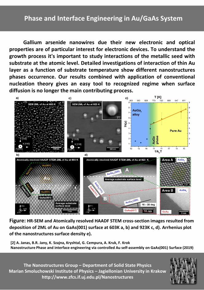
Gallium arsenide nanowires due their new electronic and opticalproperties are of particular interest for electronic devices. To understand thegrowth process it's important to study interactions of the metallic seed withsubstrate at the atomic level. Detailed investigations of interaction of thin Aulayer as a function of substrate temperature show different nanostructuresphases occurrence. Our results combined with application of conventionalnucleation theory gives an easy tool to recognized regime when surfacediffusion is no longer the main contributing process.
[2] A. Janas, B.R. Jany, K. Szajna, Kryshtal, G. Cempura, A. Kruk, F. KrokNanostructure Phase and interface engineering via controlled Au self-assembly on GaAs(001) Surface (2019)
Phase and Interface Engineering in Au/GaAs System
Figure: HR-SEM and Atomically resolved HAADF STEM cross-section images resulted from
deposition of 2ML of Au on GaAs(001) surface at 603K a, b) and 923K c, d). Arrhenius plot
of the nanostructures surface density e).
The Nanostructures Group – Department of Solid State PhysicsMarian Smoluchowski Institute of Physics – Jagiellonian University in Krakow
http://www.zfcs.if.uj.edu.pl/Nanostructures

Intensive research efforts have attracted widespread interest in the fieldof the synthesis, design and fabrication of regular semiconductornanostructures with precisely defined size and shape over large areas.Depending on the material and the individual sputtering conditions it wasobserved that self-organized unique patterns, such as ripples, dots and pillars,can evolve after high fluence ion sputtering of AIII–BV semiconductor surfaces(e.g. InSb, InP, InAs, GaSb). These nanostructures obtained with length scalesspanning from few to hundreds of nanometers can provide ideal elements infuture nanoelectronic industry including, among others, FET transistors,interconnections with larger scale devices, as well as antireflective orhydrophobic coatings.
AIII-BV Semiconductors: Ion-Beam-Induced Nanostructures
[1] B.R. Jany, K. Szajna, M. Nikiel, D. Wrana, E. Trynkiewicz, R. Pedrys, F. Krok, Appl. Surf. Scie., 327, 86 (2015)
[2] E. Trynkiewicz, B.R. Jany, D. Wrana, F. Krok, Thermally controlled growth of surface nanostructures on ion-
modified AIII-BV semiconductor crystals, Applied Surface Science, 427 349-356 (2018)
[3] Elzbieta Trynkiewicz, Benedykt R Jany, Arkadiusz Janas, Franciszek Krok
Journal of Physics Condensed Matter 30(30) (2018)
Fig. 1: SEM image of ion-beam-modified GaSb(001) surface bombarded with 3 keV Ar+ ions.
The inset represents the corresponding single structure with a scale bar of 25 nm.
Fig. 2: RGB EDX composition map of the fabricated single pillar.
Fig. 3: Photograph of irradiated phosphorus in MBE system equipped with broad-beam
ion gun.
Figure 1 Figure 2 Figure 3
The Nanostructures Group – Department of Solid State PhysicsMarian Smoluchowski Institute of Physics – Jagiellonian University in Krakow
http://www.zfcs.if.uj.edu.pl/Nanostructures

The Focused Ion Beam mounted on DualBeam FEI Quanta 3D FEGmicroscope is used for nanofabrication of various materials needed fordifferent applications in science and technology. The nanopatterns inAu/Glass could be created for the atomic/optical physics applications as aPlasmonic Transmission Gratings. As well as patterns for X-ray capillary opticsimaging. Also the FIB technique could be used for STM tip processing toproduce sharp and repeatable tip radius.
[1] B.R. Jany, K. Szajna, M. Nikiel, D. Wrana, E. Trynkiewicz, R. Pedrys, F. Krok, Appl. Surf. Scie., 327, 86 (2015)
[2] P. Korecki, K.M. Sowa, B.R. Jany, F. Krok, Physical Review Letters 116, 233902 (2016)
[3] Katarzyna M. Sowa, Benedykt R. Jany, and Paweł Korecki, Optica Vol. 5, Issue 5, pp. 577-582 (2018)
Focused Ion Beam (FIB) Nanofabrication
Figure 1: FIB sharpening of Pt/Ir STM tip a)-c), FIB nanopatterning of Au/Glass Plasmonic
Transmission Grating
The Nanostructures Group – Department of Solid State PhysicsMarian Smoluchowski Institute of Physics – Jagiellonian University in Krakow
http://www.zfcs.if.uj.edu.pl/Nanostructures

The Machine Learning (ML) techniques, which can analyze hugeamount of multidimensional data without any interaction or bias from theuser, are successfully used in Electron Microscopy. Blind Source Separation(BSS) could be applied to hyperspectral SEM EDX data at nanoscale toovercome the limitations of SEM EDX to chemically quantify nanoobjects.Another example is the application of the ML Random Forest model for theatomically resolved HAADF STEM image chemical quantification, the MLsuccessfully quantifies the image dealing with inherent noise.
Machine Learning in Electron Microscopy
a b
c d
e
f
g
Nanowires
~50nm
Overcoming limitations of SEM EDX Chemical Quantification
Figure 1: SEM EDX data collection at nanoscale in form of Spectrum Image (SI)
maps from metallic nanowires c)-d), results of Machine Learning Blind Source
Separation (BSS) e)-g), which separates EDX nanowires signal from
background, this is later quantified by EDX ZAF [1].
[1] Benedykt R. Jany, Arkadiusz Janas, and Franciszek Krok, Nano Letters, Vol. 17, Issue 11, 6507-7170 (2017)[2] B.R. Jany, A. Janas, K. Szajna, O. Kryshtal, G. Cempura, A. Kruk, A. Czyrska-Filemonowicz, F. KrokChemically driven growth of Au rich nanostructures on AIII-BV semiconductor surfaces (2019)
Figure 2: Machine Learning HAADF STEM image quantification of Au diffusion area
formed in Au/InSb nanowires system a). The Au concentration was determined separatly
for Sb and In atomic sublattice b)-c) [2].
ab c
The Nanostructures Group – Department of Solid State PhysicsMarian Smoluchowski Institute of Physics – Jagiellonian University in Krakow
http://www.zfcs.if.uj.edu.pl/Nanostructures

The Environmental Scanning Electron Microscopy (ESEM) is used forLife Science Applications for the imaging and characterization of nonconductive and biological specimens. The nanoporus drug carries could bedirectly characterize by the ESEM for pharmaceutical applications. Theinternal structure of melanoma cells was accessible by ESEM imaging. There isalso a possibility to directly characterize the surface of Red Blood Cells (RBC)and try to link it to the specific disease entity.
[1] A. Krupa, J. Szlęk, B.R. Jany, R. Jachowicz, AAPS PharmSciTech, 16, 3 (2015)
[2] J. Bobrowska, J. Pabijan, J. Wiltowska-Zuber, B.R. Jany, F. Krok, K. Awsiuk, J. Rysz, A. Budkowski,
M. Lekka, Analytical Biochemistry 511, 52 (2016)
[3] J. Bobrowska, J. Pabijan, J. Wiltowska-Zuber, B.R. Jany, F. Krok, K. Awsiuk, J. Rysz, A. Budkowski,
M. Lekka, Data in Brief, 7, 1322 (2016)
[4] A. Kamińska, M. Platt, J. Kasprzyk, B. Kusnierz-Cabala, A. Gala-Bladzienska, O. Woźnicka, B.R. Jany,
F. Krok, Journal of Diabetes Research, 2016, 5741518 (2016)
[5] Y. Stetsyshyn, K. Awsiuk, V. Kusnezh, J. Raczkowska, B.R. Jany, A. Kostruba, K. Harhay, H. Ohar, O.
Lishchynskyi, Y. Shymborska, Y. Kryvenchuk, F. Krok, A. Budkowski, Appl. Surf. Scie. 463, 1124 (2019)
Environmental Scanning Electron Microscopy for Life Sciences
Figure 1: ESEM imaging of a) Nanoporus drug carrier Neusilin US2, b)-c) Details of
Melanoma Cells internal Structure, d)-e) Surface of Red Blood Cells
The Nanostructures Group – Department of Solid State PhysicsMarian Smoluchowski Institute of Physics – Jagiellonian University in Krakow
http://www.zfcs.if.uj.edu.pl/Nanostructures
Marian Smoluchowski Institute of PhysicsJagiellonian University in Krakow
The Nanostructures GroupDepartment of Solid State Physics
Lojasiewicza 11PL-30348 Krakow
POLAND
Email: [email protected]
Phone: +48 12 664-46-32Fax: +48 12 664-49-05
The Nanostructures Group – Department of Solid State PhysicsMarian Smoluchowski Institute of Physics – Jagiellonian University in Krakow
http://www.zfcs.if.uj.edu.pl/Nanostructures