the materials science of titanium dioxide...
TRANSCRIPT

The Materials Science of Titanium Dioxide Memristors
by
Matthew Douglas Pickett
A dissertation submitted in partial satisfaction of the
requirements for the degree of
Doctor of Philosophy
in
Engineering - Materials Science and Engineering
in the
GRADUATE DIVISION
of the
UNIVERSITY OF CALIFORNIA, BERKELEY
Committee in charge:Professor Ramamoorthy Ramesh, Chair
Dr. R. Stanley WilliamsProfessor Ronald GronksyProfessor Leon O. Chua
Fall 2010

The Materials Science of Titanium Dioxide Memristors
Copyright 2010
by
Matthew Douglas Pickett

1
Abstract
The Materials Science of Titanium Dioxide Memristors
by
Matthew Douglas PickettDoctor of Philosophy in Engineering - Materials Science and Engineering
University of California, Berkeley
Professor Ramamoorthy Ramesh, Chair
This dissertation describes the materials science of memristive switching in titaniumdioxide. It discusses the strucutral changes of the oxide that take place and provides aphenomenological model for the dynamical behavior during switching. Further, the dis-sertation describes a two-state variable nanoscale device based on metal insulator tran-sitions and memristive switching. It concludes with a discussion of various applicationsof titanium oxide memristive devices.

i
Contents
1 Introduction to resistive switching in oxides 11.1 Description of the phenomenon . . . . . . . . . . . . . . . . . . . . . . . 11.2 Literature survey . . . . . . . . . . . . . . . . . . . . . . . . . . . . . . . 11.3 Dissertation summary . . . . . . . . . . . . . . . . . . . . . . . . . . . . 4
2 Microscopic characterization of functioning memristors 62.1 Experiment description . . . . . . . . . . . . . . . . . . . . . . . . . . . . 72.2 STXM characterization . . . . . . . . . . . . . . . . . . . . . . . . . . . . 72.3 TEM characterization . . . . . . . . . . . . . . . . . . . . . . . . . . . . 11
3 Dynamics of memristive switching 163.1 The canonical memristive system . . . . . . . . . . . . . . . . . . . . . . 163.2 The stress-test protocol . . . . . . . . . . . . . . . . . . . . . . . . . . . . 183.3 Device description and characteristics . . . . . . . . . . . . . . . . . . . . 203.4 Quasi-static transport model . . . . . . . . . . . . . . . . . . . . . . . . . 213.5 Dynamical model . . . . . . . . . . . . . . . . . . . . . . . . . . . . . . . 243.6 Discussion and conclusion . . . . . . . . . . . . . . . . . . . . . . . . . . 29
4 Two state variable metal-insulator transition systems 314.1 Description of Models . . . . . . . . . . . . . . . . . . . . . . . . . . . . . 32
4.1.1 Memristive barrier model . . . . . . . . . . . . . . . . . . . . . . . 344.1.2 Metal-insulator transition instability model . . . . . . . . . . . . . 35
4.2 SPICE model for time domain simulations . . . . . . . . . . . . . . . . . 384.3 Transport and switching characterization . . . . . . . . . . . . . . . . . . 404.4 Characterization of the MIT oscillator . . . . . . . . . . . . . . . . . . . 424.5 The configurable voltage-controlled oscillator . . . . . . . . . . . . . . . . 454.6 Conclusion . . . . . . . . . . . . . . . . . . . . . . . . . . . . . . . . . . . 46
5 Circuit applications of titanium dioxide memristors 475.1 The nonvolatile latch . . . . . . . . . . . . . . . . . . . . . . . . . . . . . 475.2 A defect-tolerant crossbar demultiplexer . . . . . . . . . . . . . . . . . . 52

ii
Bibliography 61

iii
Acknowledgments
None of my work would have been possible without the guidance of Stan Williams andthe long-term vision of Hewlett-Packard for supporting Labs in general and the Informa-tion and Quantum Systems Lab in particular. I am grateful to Professor RamamoorthyRamesh for serving as my advisor and facilitating the connection between UC Berke-ley and HP Labs. I am additionally indebted to my colleagues at HP Labs, especially:Julien Borghetti, Gilberto Medeiros-Ribeiro, Feng Miao, Xuema Li, Zhiyong Li, DouglasOhlberg, Warren Robinett, Greg Snider, Duncan Stewart, John Paul Strachan, DmitriStrukov, Wei Wu, Qiangfei Xia and Jianhua (Joshua) Yang. My work was financially sup-ported by Hewlett-Packard and in part by the following agencies: the DARPA SyNAPSEproject, the US Government’s Nano-enabled technology initiative and the DOE throughsupport for the Advanced Light Source and the Molecular Foundry at LBNL.

1
Chapter 1
Introduction to resistive switching inoxides
1.1 Description of the phenomenon
Nonvolatile resistance switching is a seemingly universal phenomenon exhibited bymetal oxide insulators when they are fabricated into metal-oxide-metal thin-film capacitorstructures. The qualitative behavior is straightforward: apply a sufficient voltage acrossthe metal electrodes and the resistance of the oxide permanently changes, typically byseveral orders of magnitude. The resistance can be reversed back to the original value byapplying another voltage across the electrodes. A resistance decrease is called a ‘SET’or ‘ON’ switching operation and an increase is called a ‘RESET’ or ‘OFF’ switchingoperation. Some oxides can be switched ON and OFF by applying the same voltagepolarity and are consequently labeled as unipolar, while others, labeled as bipolar, requireopposite polarities for ON and OFF switching. For both types, a so-called electroformingstep is frequently required to initiate switching from a highly resistive as-fabricated stateto a less resistive OFF/ON switching regime. This electroforming is typically achievedby applying a voltage larger than either of the subsequent OFF or ON switching voltages.
1.2 Literature survey
Resistive switching in oxides was discovered and identified for applications in solidstate memory in the early 1960s. The first reports on the phenomenon came from Hick-mott and Hiatt at GE [1, 2] and Gibbons and Beadle at Stanford [3]. The potentialapplications of this type of switching drove a flurry of study on the materials science ofoxide conduction phenomena. However, by 1971 a lack of consensus remained regardingthe following three questions:
1. Is the switching effect due to localized or uniform conduction pathways?

2
2. Is the switching due to charge trapping or ionic motion?
3. Is the effect occurring in the bulk of the oxide or at the interface with the electrodes?
The reviews of Dearnaley, Stoneham and Morgan [4] and Simmons [5] capture the essenceof the discussion at the time.
Concurrently, in 1971 Dov Frohman-Bentchkowsky at Intel produced the first prac-tical implementation of MOSFET-based floating gate charge storage memory (EPROM)[6, 7]. EPROM technology and its descendants, EEPROM and FLASH, have since domi-nated the solid state memory market mainly because they have been tied to the blisteringspeed of innovation and device scaling of silicon MOS technology. It is perhaps unsur-prising that research activity into oxide switching tapered off in the early seventies andthe phenomenon was regarded as a scientific curiosity for three decades.
Resistance switching in oxides regained interest from the scientific community inthe early 2000s when a new generation of researchers observed the phenomenon whilestudying the ferroelectric [8, 9], high dielectric constant (κ) [10, 11] and magnetore-sistive [12, 13] properties of thin film perovskite oxides. At around the same time,nanoscale crossbar circuits [14, 15] and novel computing architectures [16, 17, 18] basedon two-terminal resistive switching emerged as possible candidates to replace conven-tional CMOS. In 2006 Szot et al. demonstrated that resistive switching in oxides couldbe confined to a single dislocation in SrTiO3 [19] implying that the ultimate scalabilityfor the phenomenon is beyond 10 nm. These results indicate that resistive switching inoxides could be the go-forward technology for nonvolatile memory after FLASH hits itsimpending scaling floor at the 16 nm node in 2016 (see e.g. the Emerging Research De-vices section of the 2009 ITRS Report [20]). Although there are still technical problemsto be worked out, the promise of extending memory scaling by several generations hasspurred a resurgence of research on oxide switching in the past five years.
During this time a variety of groups around the world have employed the advent ofnew analytical techniques and improved electrical equipment to more directly answer thequestions left over from the seventies. The first question of whether or not the conductionis localized in switching oxides has been answered for a broad range of oxide phasesranging from the complex, such as single crystal epitaxial Ruddlesden-Popper phases, tothe simple, such as amorphous sputtered binary oxides. There is now consensus that forboth unipolar and bipolar switching the switching effect is almost always located to asmall region of the device which is typically defined by electroforming. By employingelectron beam induced current (EBIC) measurements, Rossel et al. showed localizedconduction pathways in switching SrZrO3 epitaxial films [21]. Choi et al. used conductiveatomic force microscope (AFM) measurements to demonstrate that switching is localizedin atomic layer deposition (ALD) grown polycrystalline TiO2 films [22]. Szot et al. alsoused conductive AFM to demonstrate the localized dislocation switching mentioned abovein SrTiO3 [19]. Jeong et al. inferred from impedance spectroscopy of polycrystalline TiO2
that the conduction pathway was localized [23]. Janousch et al. employed synchrotron-based x-ray absorption measurements to directly map a locally reduced pathway between

3
the electrodes of a planar Cr:SrTiO3 device [24]. Kim et al. inferred that switching inALD grown TiO2 films is localized from DC current-voltage (i − v) measurements [25].Sato et al. inferred a ‘thermal filament’ model from pulsed switching measurementsof sputtered NiO and TiO2 films [26]. Chae et al. proposed that unipolar switchingin sputtered NiO can be modeled as local breakdown in a resistive network based ontheir observation in that between switching events the threshold voltages appear to berandomly distributed [27]. The observation of localized features with AFM led Yang etal. to conclude that the electroforming step creates a locally reduced channel [28]. Thisobservation was later confirmed by synchrotron-based spatially resolved photoemissionspectroscopy by Strachan et al. [29]. Kwon et al. [30] reported direct observation of thelocalized channel with cross-sectional TEM for unipolar TiO2 switches while Strachan etal. [31] reported direction observation in bipolar TiO2 switches.
The fact that there is some universality to the localization of switching for vastlydifferent oxide compositions and structures indicates that the switching effect is morelikely to be related somehow to the oxygen ions in the lattice, rather than electronicstructure or trapping effects. Indeed, there seems to be broad consensus in the com-munity now that switching is related to the motion of oxygen or oxygen vacancies, asdetermined by the application of advanced techniques. Fujimoto et al. used electronenergy loss spectroscopy (EELS) to demonstrate that TiO2 is reduced, or has a highvacancy concentration, in the switching region [32]. Karg et al. used temperature de-pendent electron transport measurements to infer that resistance changes were relatedto the presence of vacancies which act as hopping centers [33] in SrTiO3. Fujii et al.and Jameson et al. respectively came to a similar conclusion using similar techniqusfor epitaxial SrTi1−xNbXO3 [34] and bulk single crystals of TiO2 [35]. As mentionedabove, Janoush et al. was able to directly image a reduced channel in SrTiO3 using XASmapping [24]. Hirose et al. [36] and Phan et al. [37] used impedance spectroscopy toinfer that vacancy motion was responsible for switching in SrTiO3 . Hasan et al. alsoused pulsed electrical measurements to conclude that vacancy migration is responsiblefor switching in La0.7Ca0.3MnO3 [38]. Jeong et al. [39] and Yang et al. [28] showed withAFM that electroforming of TiO2 materials causes features to appear on top electrodes,reportedly due to oxygen evolution during the forming process. Yang et al. used conduc-tive AFM and electrical measurements to demonstrate that electrical switching is alsomediated by vacancy motion in Ca doped BiFeO3 grown on SrTiO3 [40]. Strukov et al.developed the first complete quantitative model for bipolar switching in oxides based onvacancy drift/diffusion [41] and showed that this model is equivalent to the memristorelement predicted theoretically by Chua [42]. Strukov et al. later expanded this simplemodel to account for nonlinearities in electronic and ionic [43, 44] transport. Jeong etal. published a similar model for switching in TiO2 based on vacancies modulating thebarrier height of an interface Schottky barrier [45].
The relationship between vacancy motion and total device resistance was the thirdremaining question for the switching mechanism and turns out to be the main differ-ence between the material mechanisms for bipolar and unipolar switching in oxides. For

4
bipolar switching in thin films the consensus that exists now points to a modificationof the contact resistance between the oxide and the electrodes rather than the oxidebulk. Various researchers have come to this conclusion from transport and impedancespectroscopy measurements on epitaxially grown Schottky barriers of the model sys-tems Pr0.7Ca0.3MnO3 [46], SrTi1−xNbxO3/SrRuO3 [47, 34] La1−xSr1+xMnO4 [48] andSrTiO3[37]. Other researchers came to similar conclusions for Schottky barriers fabri-cated from ceramic SrTiO3[36], sputtered La0.7Ca0.3MnO3 [38], SrTiO3 bicrystals [49],bulk single crystals of Rutile TiO2 [35, 50] and sputtered TiO2 [50]. Miao et al. used themore direct method of pressure modulated conductance microscopy to demonstrate thatbarrier width modulation is the likely switching mechanism in Pt/sputtered TiO2/Ptdevices [51]. Borghetti et al. used temperature dependent transport measurements tostrengthen this model [52]. As discussed above, Strukov et al. [41, 43, 44] and Jeong etal. [45] have developed quantitative models based on vacancy modulation of interfacebarriers in bipolar devices.
For unipolar switching the original model of Gibbons and Beadle [3], based on current-driven creation/rupture of reduced shunt channels through the bulk of the film, remainslargely intact. Chae et al. have updated the model in the context of random resistornetworks to account for switching variability [27]. Kwon et al. have shown direct TEMevidence that a metallic reduced oxide of Ti4O7 channel bridges the two electrodes in theON state, but is incomplete in the OFF state of a unipolar Pt/TiO2/Pt switch [30].
1.3 Dissertation summary
In this dissertation I report the results of five research efforts that I either advancedor contributed significantly to during the past three years. Chapter 2 shows the results ofan effort to directly characterize the material structure of switching centers in a function-ing device using TEM and synchrotron-based scanning transmission x-ray microscpec-troscopy (STXM) and is based on reference [31]. The results unambiguously demonstratethat the switching effect is localized and that the conduction channel is composed of areduced metallic phase. Chapter 3, based on reference [53], reports a dynamical electrialcharacterization of oxide switching and presents a state-variable based memristive modelto accurately and quantitatively predict device behavior. This work ellucidates the highlynonlinear processes taking place in the oxide during switching for both the electronic andionic motion. Chapter 4, based on reference [54], builds upon the previous memristivemodel and knowledge of conduction channel phase analysis to experimentally demon-strate a nanoscale device that exhibits both memristance and metal-insulator transition.This device is shown to produce self-sustained oscillations when biased with a DC voltagebased on a threshold instability of the metal-insulator transition which, when coupledwith the memristance, can be used for tunable oscilators. The final chapter shows theexperimental demonstration of two circuit applications enabled by the memristive prop-erties of metal-oxide-metal devices: the defect-tolerant demultiplexer, based on reference

5
[55], and the nonvolatile latch, based on reference [56].

6
Chapter 2
Microscopic characterization offunctioning memristors
A full understanding of the atomic-scale mechanism and identification of the mate-rial changes within titanium oxide during memristive switching remains an importantgoal. In this chapter (previously published in part in reference [31]), we report the char-acterization of a functioning TiO2 memristor using synchrotron-based x-ray absorptionspectromicroscopy and transmission electron microscopy (TEM). We observed that elec-troforming of the device generated a crystallite of the Magneli Ti4O7 phase within theinitially sputter-deposited TiO2 matrix. In an attempt to describe microscopically thesource of the resistance change, many physical models have been put forth, includinggeneration and dissolution of conductive channels [57, 58], electronic trapping and space-charge current limited current effects [59], strongly correlated electron effects such as ametal-insulator transition [60], and changes localized to the interface of the metal elec-trode and the oxide [46, 19]. Identifying the correct model and quantifying its physicalparameters using exclusively electrical characterization has not entirely eliminated theambiguity between these available models. Meanwhile, direct physical characterization[24] requires the capability of observing subtle material changes, such as vacancy creation,occurring in a nanoscale volume buried between two metal contacts. Recently, Kwon,et al. [30] performed cross-sectional TEM studies of the unipolar resistive switching inTiO2, revealing the presence of nanoscale Magneli phase conductive channels followingdevice operation and extraction of a region of interest. A Ti4O7 phase was confirmed fromthe temperature dependence of the conductance. Concurrently, we have investigated thebipolar memristive switching mode of TiO2, using non-destructive transmission-geometryspatially-resolved x-ray absorption and electron diffraction to report on the associatedchemical and structural changes of a functioning device.

7
2.1 Experiment description
To enable the transmission measurements, a vertical metal-insulator-metal (MIM)crosspoint device was fabricated on a thin free-standing Si3N4 window, as illustrated inFigure 2.1a. The device stack consisted of Cr(5)/Pt(15)/TiO2(30)/Pt(30 nm) grown ona Si/Si3N4 (20 nm) substrate. The device consisted of a 2 µm wide bottom electrodeand a 3 µm wide top electrode patterned perpendicular to each other with their overlapdefining the active junction area. The junction was centered within the 60×60 µm2
free-standing window (Figure 2.1b). The TiO2 switching layer, which extends across theentire substrate, was sputter deposited from a titania source onto the substrate held at250 C.
Following an initial electroforming step, the device exhibited reversible bipolar re-sistance switching (Figure 2.1c) between a low resistance of 20 kΩ (ON) and a highresistance of 1 MΩ (OFF), as measured at low bias. One issue of concern was whetherdevices fabricated on thin windows would behave similar to devices on thicker substrates;strain effects and the inability to sink the significant Joule heating generated during op-eration [29, 52] might change the device electrical characteristics. A comparison of theelectrical switching in Figure 2.1c shows that window devices have similar switching be-havior to standard devices fabricated on a silicon oxide substrate. The latter have beenextensively characterized electrically [53], and show bipolar, non-volatile switching downto sizes of 50 nm (half-pitch) and speeds 10 ns.
Electrical characterization of the device was performed in a four-probe geometry usingan HP4155 semiconductor parameter analyzer, with the bottom electrode grounded at alltimes. The electroforming step (inset to Figure 2.1c) was performed as a slow (∼1 sec) 0to -8 V sweep, leaving the device roughly 106 times more conductive. The comparison inFigure 2.1c shows a standard device (red, dashed) which has an identical materials stack,except uses a Ti adhesion layer rather than Cr. Transmission devices studied in thispaper used Cr in order to avoid any Ti background signal. After performing 6 ON/OFFswitching cycles, the device was characterized by STXM and TEM.
2.2 STXM characterization
X-ray measurements were performed using the Scanning Transmission X-ray Micro-scope (STXM) at the Advanced Light Source in Lawrence Berkeley National Laboratory1.STXM allows spatially-resolved x-ray absorption spectroscopy (XAS) to be performed ona sample by raster-scanning a focused, monochromatic x-ray beam that can be tuned inenergy with better than 100 meV resolution [61]. Focusing of the x-rays is accomplishedusing a diffraction-based Fresnel zoneplate lens, which can give a spatial resolution of
1STXMmeasurements and analysis were performed on this sample exclusively by John Paul Strachan,but are included here with permission because they are complementary to the TEM data analysisperformed by the author

8
Figure 2.1: Illustration of the device geometry for transmission characterization. a) Across-bar device is aligned to a free-standing silicon nitride window in which the un-derlying silicon substrate has been fully etched away in a 60×60 µm2 area. A bottomand top electrode are defined in separate photo-lithography steps, with an unpatternedtitanium dioxide layer in between. b) Optical micrograph of a completed device. c) Elec-trical characterization of the titanium dioxide memristor before physical measurements.Following an electroforming step (inset), the device shows bipolar resistance switching(solid green trace) to an ON state with positive bias and to an OFF state with negativebias. Comparison to a standard, non-window device fabricated atop a silicon/siliconoxide substrate is also shown (red, dashed).

9
roughly 35 nm. The absorption of x-rays by the sample is measured in a transmissiongeometry. In our study, a sequence of images of the device junction area was acquiredat incremental photon energies and spatially localized spectra were generated by postprocessing this absorption versus energy data set within various regions of the sample.
After electroforming and switching of the device, STXM measurements were per-formed within the junction area while scanning the incident monochromatic x-ray energy.With this technique, the switching layer can be isolated from the Pt electrodes and othermaterials in the stack by tuning the x-ray energy to a Ti resonance, in this case the TiL2,3 absorption edge (455 - 475 eV). The observed absorption intensity is proportional tothe unoccupied density of states, broadened by the core-hole lifetime, and can act as afingerprint to identify the phase and chemical state of the titanium [62, 63, 64]. Figure2.2a shows an x-ray image of the junction taken at a single energy within the Ti edge,illustrating the absorption contrast within the device. In this image, increased absorptioncorresponds to darker regions, and the main contrast observed here is primarily based onmaterial thickness and elemental mass, with the Pt electrodes dominating in absorption.However, a region near the center of the device possessing chemical contrast is alreadyevident. Full processing of the energy-dependent stack of images across the Ti L-edgerevealed the presence of three distinct states of the titanium oxide switching layer andthe corresponding absorption spectra are shown in Figure 2.2c. Figure 2.2b providesa spatial mapping for the three states of the oxide, with regions labeled i, ii, and iii.For similar devices with no prior electrical treatment (“virgin state”), no such chemicalfeatures are observed.
Region i is outside of the junction area and is most similar to the as-deposited TiO2,which is known from X-ray Diffraction (XRD) to be an amorphous phase. Within thejunction (region ii), the spectrum strongly matches the known XAS for anatase, one ofthe crystalline polymorphs of TiO2 [63, 64]. This crystalline phase shows a noticeablesharpening of the absorption peaks, particularly the first and third main peaks (near 458and 463 eV) and an increased crystal field splitting. Additionally, a prominent splittingof the second main peak (near 460.5 eV) is observed due to the distortion [62, 63, 64] ofthe Ti site from octahedral to tetragonal symmetry. This crystallization of the depositedtitanium dioxide has been observed [29] in resistance switching devices and is driven byJoule heating, which can raise the device temperature above 350 C in spatially localizedregions [52]. Figure 2b indicates that the crystallized region extends along the bottomelectrode, possibly because of the reduced thickness and width compared to the topelectrode.
Most striking is region iii, an approximately 200×300 nm2 area that has a qualitativelydifferent absorption spectrum (Figure 2.2c , blue spectrum) from those of regions i andii. Here, the spectrum exhibits a pronounced shift in density to lower energies (newfeatures at 456 eV and 461.3 eV), as well as a merging of the crystal-field split doubletpairs. These changes result from core-level shifts, [65, 66, 67, 68] indicating a mixed-valence composition in region iii of Ti+3 and Ti+4, and closely matching the spectralshape and trend [68, 69] for deliberately reduced titanium oxide layers. This is a direct

10
Figure 2.2: Chemical and structural mapping of a functioning memristor by ScanningTransmission X-ray Microscopy (STXM) following electroforming and ON/OFF cycling.a) STXM image of the device junction area, taken at an x-ray energy of 460.0 eV withinthe Ti L3 edge. Absorption contrast is observed within the junction. b) Chemical andstructural mapping of the three observed phases of titanium oxide. Region i (green)is the as-grown amorphous TiO2, region ii is the anatase phase, and region iii shows astoichiometrically reduced suboxide TiO2−x, or equivalently a mixed-valence oxide withTi+3 and Ti+4 ions. The color mapping of each pixel is derived from the Ti L2,3 x-ray ab-sorption spectrum using singular value decomposition procedures. c) The correspondingTi L-edge x-ray absorption spectra.

11
observation of a locally reduced region within the functioning bipolar resistance switch.Since reduction of titanium dioxide leads to metallic conductivity, and is not presentin a virgin device, it follows that this observed region is responsible for the dramaticconductivity increase after electroforming of the junction.
2.3 TEM characterization
Complementing the chemical analysis, localized structural information was acquiredby transmission electron microscopy (TEM) and nanobeam diffraction on the same de-vice. TEM measurements were performed on a JEOL 2100F equipped with a GatanImaging Filter operating at 200 kV. At various locations within the device, electrondiffraction images were acquired using a nanobeam spot sizes of 50 to 200 nm. Diffrac-tion pattern images were calibrated to a Si [100] zone axis pattern measured on the samesample at the edge of the window.
The upper right corner of the device was first characterized in order to determinethe structure of the oxide in the regions i and ii of the STXM map in Figure 2.2b. Atransmission image of the corner region is included as Figure 2.3a with the four circlesindicating where the nanobeam diffraction measurements were taken. The position ofthe diffraction spots were chosen to determine the phases present in the top electroderegion, bottom electrode region, junction region, and the window or TiO2 only region. Asdemonstrated by the radially-integrated diffraction data of Figure 2.3b, the top electrodeshows only Pt diffraction spots since the TiO2 is amorphous. Both the bottom electrodeand the junction regions show the signature of Pt and anatase crystals. These resultsare identical to those obtained from STXM which determined that region i is amorphousand region ii is anatase. Diffraction data from the TiO2 in the window spot is not shownbecause it is amorphous and there were no spots in the diffraction image.
The electron diffraction pattern observed within the reduced region iii of Figure 2.2bis shown in Figure 2.4a and revealed a single crystal of Ti4O7, consistent with the spec-troscopic results of the previous section. The phase of this crystallite was identifiedby reconciling the strongly diffracting spot positions with possible diffractions from allknown phases in the Ti-O binary phase diagram. The diffraction spot positions wereinitially identified by comparing the magnitudes of the observed scattering vectors in themeasured pattern to all possible scattering vector magnitudes of 17 phases we consideredplausible. We used the database in the Phillips Analytical X’Pert software to generatea list of possible scattering vector magnitudes from the following crystal structures: theAnatase, Rutile and Brookite polymorphs of TiO2, the series of Magneli phases TinO2n−1
for n=3-10, the corundum structure Ti2O3, the cubic and hexagonal polymorphs of TiO,and the electrode metals Ti, Pt and Cr. Ti4O7 emerged as the only consistent structure.
The phase identification was confirmed by simulation of the Ti4O7 diffraction patternusing the reported structure [70] with SingleCrystal from Crystal-Maker Software. Wefound excellent agreement when the simulated zone axis is taken to be the lattice vector

12
81
2
3
4
5678
Cou
nts
(a.u
.)
108642|g| (1/nm)
Bottom electrode Junction area Top electrode
Anatase Pt
(a)
(b)
Figure 2.3: (a) TEM image showing a zoom on the upper right corner of the device withwhite circles indicating the positions of nanobeam diffraction measurements. (b) Radiallyintegrated diffraction patterns from the spots of interest with vertical lines indicatingpossible scattering vector magnitudes for Pt and anatase. Comparison of the integratedprofiles and possible peak positions shows that the TiO2 is amorphous beneath the topelectrode, but is in the anatase phase above the bottom electrode and in the junctionregion. These spots correspond to regions i and ii respectively of the STXM map ofFigure 2.2b.

13
[uvw] = [1.1, 1.7, 0.3], as indicated by the alignment of calculated (blue circles) and mea-sured spot positions indexed in Figure 2.4a. The lateral size and shape of the crystallitewas revealed to be ∼ 100×50 nm2 by dark field imaging with an aperture around the104 spot as shown in Figure 2.4b.
Since the measurement was done on a device buried underneath platinum electrodesand embedded in an anatase matrix, the electron beam also transmitted through crys-tallites of Pt and anatase. Additional diffraction spots not associated with the reducedcrystallite of interest are thus visible on the same pattern. The red and grey rings su-perimposed on the diffraction pattern indicate possible diffraction positions from anataseand Pt, respectively, showing that these other observed spots are likely background fromthese phases.
The observation of the Ti4O7 phase is consistent with the localized reduction seen inSTXM, but also reveals an ordering of the oxygen vacancies in region iii of Figure 2.2b.Ti4O7 is a member of the homologous series of stable reduced TiO2 phases, frequentlyreferred to as the Magneli phases, and has a metallic conductivity at room temperature[71]. The crystallographic structure is similar to that of the common rutile phase ofTiO2, but with ordered periodic planes of oxygen vacancies. The small area observedfor the Ti4O7 crystallite (Figure 2.4b) indicates that ordering of the vacancies occurredwithin a sub-region of the reduced area (blue region of Figure 2.2b), possibly where Jouleheating was highest during electroforming. Additional crystals of Ti4O7 and even higherorder Magneli phases may also be present in this region, but were not obvious from themeasurements that we performed.
A more complete picture describing the mechanism for bipolar resistive switchingthus emerges when the results of both the physical and electrical characterization arecombined. Prior studies [52] of titanium dioxide memristors have shown that the elec-trical data is best modeled as a metallic element in series with a tunneling gap or othernon-linear transport barrier. Additionally, studies using the technique of pressure mod-ulated conductance with an AFM tip [51] show that insulating barrier width modulationis responsible for the switching mechanism. By applying this model to dynamical mea-surements [53] we have additionally suggested that ON and OFF switching involves thecontraction or expansion, respectively, of this gap width by less than 1 nm. In the presentdevice, the non-linear i − v curve and low currents observed in both the ON and OFFstates (Figure 2.1c) indicate that the observed metallic Ti4O7 phase does not entirelyspan between the bottom and top electrodes. Given the geometry of our transmissionmeasurements, a resulting model (Figure 2.4c) is that resistive switching consists of amodulation of a barrier between Ti4O7 and the contacting electrodes. The modulationcan either be of the barrier width (thickness of un-reduced titanium oxide) or height [45]:drift of oxygen vacancies from the Ti4O7 by an applied electric field reduces the barrierand increases the conductivity (ON switching), while the reverse motion induced by theopposite polarity field increases the barrier (OFF switching). Directly observing such abarrier modulation remains a future goal, but is exceptionally difficult for devices in themetal-insulator-metal geometry.

14
Figure 2.4: TEM characterization of the same memristive device as in Figure 2.2. a)Electron diffraction pattern taken within the reduced region (Figure 2.2b , region iii) ofthe device with a 50 nm nanobeam spot. Red and gray circles are superimposed on thediffraction pattern indicating possible diffraction rings from polycrystalline anatase TiO2
and Pt, respectively. Indexed blue circles are the results of simulation by Single-Crystalsoftware. b) Dark field imaging of the Ti4O7 Magneli crystallite using the 104 diffractionspot showing a size of less than 50×100 nm2. c) Resulting physical model for bipolarresistance switching of Pt/TiO2/Pt memristors. The Ti4O7 acts as a source and sink ofoxygen vacancies; application of an electric field pushes vacancies into or out of a thinbarrier layer, thus modulating the barrier and switching between the ON and OFF states.

15
The observation of a Magneli crystallite in a titanium dioxide matrix shows thatbipolar resistance switching in an electroformed Pt/TiO2/Pt memristive system is re-lated to a localized partial reduction of titanium dioxide and crystallization of a metallicconducting channel. Inside a titanium dioxide matrix, the Magneli phases are thermo-dynamically favored over a high concentration of randomly distributed vacancies [72],and thus they can act as a source or sink of vacancies in the matrix material dependingon the electrochemical potential within the device. The application of an electrical biascan control vacancy motion into and out of this sub-oxide phase, modulating a transportbarrier and leading to the dramatic conductivity change.

16
Chapter 3
Dynamics of memristive switching
A significant challenge to the widespread adoption of memristive oxide switches bycircuit designers has been the lack of a predictive compact model that can be integratedinto a time domain simulation package like SPICE. The desired circuit element modelshould abstract, parameterize, and predict the behavior of the device under an arbitraryvoltage and current bias, at least under some restricted domain of state and/or excitation.Such a model has not been available for bipolar oxide switches, despite the significantprogress in understanding their physical switching mechanism in the context of coupledelectronic and ionic conductors[57, 58, 24, 73, 74, 45, 43, 44]. As discussed in detailbelow, the memristive system [75] is the most appropriate framework for achieving thegoal of quantitatively modeling these bipolar switches in the simplest way possible.
In this chapter (previously published in part in Reference [53]), we propose a dy-namical electrical testing protocol and we establish a quantitative memristive model ofbipolar switching for Pt-TiO2-Pt crosspoint devices from the results. We analyze boththe static electronic conduction behavior and the switching dynamics that arise fromionic motion in the device. Our analysis quantitatively establishes that electronic con-duction in these devices can be parameterized by a single dynamical state parameter:an insulating barrier width w that varies with time under an applied voltage or current.We see that the dynamical behavior for OFF and ON switching is highly nonlinear andasymmetric. We interpret these observations in terms of a moving phase boundary whichis mediated by an exponential dependence of the drift velocity of ionized dopants on theapplied current or voltage, and the competing or cooperative behavior of ionic drift anddiffusion, depending on the switching voltage polarity.
3.1 The canonical memristive system
The framework of a single state variable memristive system was defined by Chua andKang [75] as two coupled equations of the form:
v = R(w, i) · i (3.1)

17
150
100
50
0
Cur
rent
(µA
)
210Voltage (V)
7V, 50 ms 7V, 50 µs 10V, 50 µs
Figure 3.1: Three triangular OFF-switching voltage waveforms applied to a typical TiO2
device prepared in the same initial condition demonstrate that these bipolar switchesexhibit the four main properties of memristive systems: zero-crossing, frequency depen-dence, amplitude dependence, and continuous states.
w = f(w, i) (3.2)
In this formalism Equation (3.1) is the quasi-static electronic transport relation in whichR is a generalized nonlinear resistance function that depends on the applied current iand the instantaneous value of the state variable w. Equation (3.2) is the dynamicalor rate equation, in which w is the time derivative of the state variable and f is thegeneralized form of the differential equation which depends on both w and i. Thisformulation provides the mathematical framework for revealing the device physics andusing the memristive devices in a circuit. Here we use a current-controlled memristivesystem rather than a voltage-controlled system because it enabled us to use an analyticalexpression for the differential equation in our device model.
The generalized memristive system is a natural way to model oxide bipolar switchesbecause it can reproduce the four important phenomena exhibited by these devices.These phenomena include the zero-crossing property, a time dependent i − v shape, anamplitude dependent i − v shape, and a continuous set of possible states. These fourproperties are shown for OFF switching in the time-sampled i − v data of Figure 3.1for a typical TiO2 device under the application of a triangular voltage waveform witha variable amplitude and period. In this data the applied voltage is not equal to themeasured device voltage because the series resistance of the nanowire electrodes holdsa majority of the voltage. This voltage drop is removed from the data by performingfour-wire measurements.
The first memristive property is obvious, but not trivial: all i − v curves cross the

18
origin, or equivalently all curves exhibit ‘pinched hysteresis’. This means that no energyis stored in a purely memristive device, which is the case for all bipolar switches that westudied. The second memristive property is illustrated by the two 7 V amplitude curves:when the voltage is swept quickly, there is no change in device state and consequently nohysteresis in the i − v. However, when the voltage is swept slowly the device is able tochange state and the loop opens up. The third memristive property is illustrated by thetwo 50 µs sweeps: when the applied voltage amplitude is increased from 7 V to 10 V thehysteresis loops open up. The fourth property is embodied in the two i− v curves whichexhibit switching: the device proceeds though a continuum of states while it switchesuntil the current level is too low to cause further switching. This data makes it clear thatthese devices must be modeled as continuous dynamical systems and that the memristivesystem is an appropriate framework to use for that task.
3.2 The stress-test protocol
In order to track the state of the device throughout the switching process and obtainquantitative dynamical information, we have performed a quasi-static stress-test protocolsummarized schematically in Figure 3.2. Using a two-step iterative process, we firstapply a low voltage amplitude (too low to result in observable switching or hysteresis)triangular external voltage sweep to interrogate the state of the device as defined by itsi−v characteristic, and then apply a constant voltage time-sampled stress pulse to changethe state of the device. This process is iterated until the junction has fully switched orthe maximum test time has been reached.
In order to study the switching dynamics over six orders of magnitude in time, wefixed the amplitude of the applied voltage during each pulse but exponentially increasedthe pulse widths from one step to the next. This protocol required that the state beinvariant when the device was not under a voltage pulse intended to change the state,i.e. it must be nonvolatile and the applied test waveform must be non-perturbative.This was a good assumption for our devices and our measurement protocol, since in ourexperience the devices stay at an arbitrary state without changing for at least a year inair at room temperature and we did not observe any hysteresis in the state-interrogationi− v characteristics.
In the study presented here we examined the applied voltage dependence of OFF-switching dynamics for the device by applying a set of six state tests with pulse heightsranging from 3.0 V to 5.5 V. Additionally, we examined the applied voltage dependenceof the ON-switching behavior at -1.25 V and -1.4 V. Each test had a total of 40 voltagepulses, which gave a total time under the applied voltage of 33 seconds. After eachapplication of the state test, we reset the device to its initial condition with a quasi-dctriangular voltage sweep of the opposite polarity.
Although we held the applied or external voltage fixed during the state tests, therewas an appreciable voltage dropped on the 2 kΩ electrodes. The actual or internal

19
1.0
0.5
0.0
Vol
tage
(V
)
Test Pulse
-400
-200
0
200
400
Cur
rent
(nA
)
0.80.60.40.20.0Time (s)
8040µA
Figure 3.2: The stress-test protocol is designed to slightly push the state of a memristivedevice with a time-sample stress pulse (blue) and test for resulting changes in the i− vshape. In general it is necessary to make four-wire measurements and use full i− v testsweeps in order to precisely observe changes in the nonlinear conductivity over time.This protocol implicitly assumes there is no state relaxation between stress pulses, anassumption that we have validated for our TiO2 devices.
20
voltage, v, seen by the device was lower than the applied voltage and evolved continuouslythroughout the switching process because of the voltage divider it formed with the seriesresistance of the electrodes. The current seen by the device during a test, i, also changedthroughout the switching process. The electrode series resistance and the nonlinearity ofthe conductivity yield a complicated relationship between the current and the externaland internal voltages throughout the switching process. This behavior highlights thenecessity of a four-wire time-sampled measurement scheme to completely characterize thestate evolution during memristive switching. We accounted for these measured changesin stress voltage and current in our analysis and determination of the characteristicmemristive equations for the device.
3.3 Device description and characteristics
For our experiments, we fabricated single crosspoint metal-oxide-metal switches onthermally oxidized silicon substrates with the following vertical structure: Si / SiO2(100)/ Ti(5) / Pt(15) / TiO2(50) / Pt(30), where the numbers in parentheses are the layerthicknesses in nanometers. The TiO2 was grown by sputter deposition from a rutiletarget onto a substrate held at 250C. X-ray diffraction (XRD), transmission electronmicroscopy (TEM) and Rutherford backscattering spectrometry (RBS) analyses on sisterfilms of TiO2 grown with the same process showed that the layers are amorphous ornanocrystalline (TEM/XRD) and the as-grown stoichiometric ratio (RBS) of oxygen totitanium is 2.00±0.1.
In order to minimize the series resistance and the parasitic resistance-capacitance(RC) time constant of the wires and contact pads for time-sampled measurements, wepresent here the results from a large-area 5×5 µm2 crosspoint device. We performed sim-ilar experiments and analyses on a total of 5 devices with 4 different areas on 5 indepen-dently fabricated samples, including 50×50 nm2 devices defined by imprint lithography.The dynamical switching behavior was relatively insensitive to device size, presumablybecause the electroformation process creates the localized conduction channel describedin the previous chapter.
We electroformed the TiO2 devices by applying a voltage sweep from 0 V to +6 Vover 5 ms. As discussed in the previous chapter, electroforming causes localized heatingand oxygen vacancy formation in these materials and produced an irreversible decrease inthe resistance from the ∼ 1 G Ω as-fabricated state to the ∼ 1-100kΩ ON/OFF switchingregime. Based on the characterization outlined in the previous chapter, we believe thatthe result of electroforming was a conducting channel with a resistance in the hundredsof Ohms that shunts most of the oxide film. The electroforming also produced a remnantinsulating gap between the conducting channel and the opposite Pt electrode. Herewe assume that the width, w, of the insulating gap can be modulated by applying avoltage across the device which induces the motion of ionized defects. A schematic ofthis switching model and a representative switching i− v characteristic for these devices

21
10-8
10-7
10-6
10-5
10-4
10-3
Cur
rent
(A
)
-1 0 1Voltage (V)
(b)
V
w
Rs
Pt
TiO2 TiO
Pt
(a)
S
A
OFFON
x
Figure 3.3: The material model that we use to understand TiO2 memristive systems isshown in (a). An electroformed reduced channel bridges the majority of the oxide regionwith a residual insulating region of width w. Four-wire stress test measurements areperformed by attaching a voltage source S to the top electrode, a current amplifier A tothe bottom, and a voltage amplifier V between the two. The memristive state w is mod-ulated by applying a stress voltage for a fixed amount of time. A quasi-static i− v curve(b) qualitatively demonstrates the memristive switching hysteresis with OFF switchingoccurring for positive voltages and ON switching occurring for negative voltages.
are included in Figure 3.3. The series resistance intrinsic to the channel can be obtaineddirectly from the switching i − v by fitting the differential resistance at high bias. Forthe device reported in detail here, the value obtained was Rs = 215± 6Ω.
3.4 Quasi-static transport model
As discussed above, the generation of the memristive model from stress-test data ispossible because the state of the device is tracked with low-voltage i − v sweeps whilethe stress pulses step the state by a small amount. The test i− v data gives informationon the instantaneous memristive curve shape, but no direct information about the state.

22
Direct information is obtained by fitting the i−v curve to a conduction model in order toreduce the data into a single state parameter. Based on our previous understanding of thephenomenology of switching and in order to simplify the model as much as possible whilestill maintaining phenomenological accuracy and physical relevance, we assume that theonly material parameter that changes during switching is the width of the insulatinggap. We also assume that the only electron conduction mechanisms that are importanthere are electron tunneling through the gap and ohmic conduction in the channel. Theseassumptions allow us to generate a particular form for the first memristive equation:the static transport relation of Equation (3.1). Here we use the Simmons simplificationfor tunneling which accounts for image charges barrier lowering [76] because it providesa relatively simple but accurate closed-form expression for the i − v curve shape. Thecombination of this tunneling expression plus the channel series resistor (as shown inFigure 3.3) yields a coupled set of equations for the conduction model:
i =j0A
∆w2
[φI exp
(−Bφ1/2
I
)− (φI + evg) exp
(−B(φI + evg)
1/2)]
(3.3)
vg = v − vR = v − iRs (3.4)
with simplification terms in the equations defined by Simmons as:
j0 = e/(2πh) (3.5)
φI = φ0 − evg(w1 + w2
2w
)−(
1.15λw
∆w
)ln
[w2(w − w1)
w1(w − w2)
](3.6)
B = 4π∆w√
2m/h (3.7)
∆w = w2 − w1 (3.8)
w1 =1.2λw
φ0
(3.9)
w2 = w1 + w
[1− 9.2λ
3φ0 + 4λ− 2evg
](3.10)
λ =e2 ln 2
8πκε0w(3.11)
Here v is the internal voltage across the whole device, vg is the voltage across the insulat-ing gap, vR is the voltage across the metallic channel series resistance, the state variablew is the barrier thickness, κ is the dielectric constant, φ0 is the effective barrier height,Rs is the channel series resistance, and A is the cross-sectional area of the tunneling gap.The other symbols have their usual meanings as physical constants. Due to the seriescoupling between the gap and the channel and the complexity of the transport equation,i− v curves can only be solved by a numerical root finding procedure.
Figure 3.4 shows the test results of a 4.5 V OFF-switching stress-test on the de-vice studied in detail in this chapter. The evolution of the i − v curve shape during

23
10-6
10-5
10-4
10-3
i (A
)
-0.1-1 v (V)
t=0 s 110 µs 790 µs
Model
0.1 1
4.7ms 28 ms 160 ms
970 ms 5.7 s 33 s
t
Figure 3.4: A series of test i−v curves demonstrates the nonlinear change in curve shapeas the device is continually turned OFF with positive stress pulses of increasing width.The markers show experimental transport data for a given total time under stress, fromwhich a particular value of the state variable w is extracted. The solid lines indicate theresults of the tunneling transport model which is used to infer the w values.

24
OFF-switching is shown in detail: the device is shown to become more resistive but alsoqualitatively more nonlinear, a phenomenon that must be accounted for in an accuratememristive model. We successfully reduced the i− v characteristic for each state of thedevice to a single variable by fitting to the above conduction model. The tunneling gapwidth w as a single state variable was able to successfully reproduce the full nonlinearevolution, as shown by the model fits of Figure 3.4. For completeness we also consid-ered the tunneling barrier height φ0 as a plausible single state variable, but could notaccurately reproduce the experimental data by varying only the barrier height duringthe fitting procedure. Thus, we believe that the switching effect is primarily due to aneffective tunneling distance modulation.
For the i − v fitting we implemented an orthogonal distance regression procedure,based on ODRPACK [77]. We used a nested loop regression procedure in order tooptimize the parameters A, φ0 and κ for the entire data set simultaneously while w wasfit individually for each of the forty i−v characteristics. Invariant device parameters thatresulted were: barrier height φ0 = 0.95±0.03eV, dielectric constant κ = 5±1 and channelarea A = 10, 000 ± 2, 500nm2. The series channel resistance, Rs = 215Ω was kept fixedduring the fitting procedure because it was measured directly. The barrier width w variedfrom 1.1 nm to 1.9 nm, with typical fitting uncertainty ±0.1 nm. Typical relative errors inthe current and voltage measurements were 1%, but for the sake of clarity error bars areomitted from Figure 3.4. Assuming a cylindrical geometry for the conduction channel,the best fit area A corresponds to a diameter of 110 ± 10nm, which is consistent withprevious direct measurements of the channel width in similar devices using the techniqueof pressure-modulated conductance mapping [51] as well as the results presented in thelast chapter. This channel geometry yields a resistivity estimate of 4× 10⁻³ Ω cm whichis significantly more resistive than metallic Pt or Ti but reasonable for reduced TiO2 [78][79].
We assumed that the tunneling effective mass was equal to the free electron mass, be-cause we do not have an independent means to measure this value. This could produce asystematic error in the above parameters and the reported barrier widths. For this reasonthe numerical results should be considered as effective values, although they nonethelessprovide a good idea of the measurement precision. Invariant parameter values were ob-tained from a first regression analysis, e.g. at a particular voltage pulse amplitude, afterwhich only w was allowed to vary in subsequent fits. This procedure enabled us to trackthe width of the tunnel barrier as a function of time and applied voltage and consequentlydetermine the dynamical behavior of these devices.
3.5 Dynamical model
By reducing each state i − v to a value of w we were able to examine the voltage-dependent dynamics of the effective barrier width during switching. Figure 3.5a showsthe time evolution of w during six OFF-switching tests with external voltages ranging

25
from 3.0 V to 5.5 V. Figure 3.5c shows the results of five ON-switching tests with voltagesof -1.25 V and -1.4 V. We chose to study only two biases for ON-switching because theswitching speed was much faster and more sensitive to the magnitude of the applied biasand we had a RC-limited time resolution of (∼ 1µs) in our test setup. ON-switching re-peatability was therefore demonstrated via multiple stress tests at the same voltage. Thedevice state evolved in a continuous but highly nonlinear manner between the ON andOFF states, and the switching speed was strongly dependent on the current magnitudeand polarity. In order to determine a particular form for the second memristive equation(dynamical state evolution Equation 3.2) for OFF- and ON-switching, we again applieda orthogonal distance regression technique.
The end result was a set of consistent parameters for the full range of applied voltagesstudied, with the following analytical expressions for OFF switching:
wOFF = fOFF sinh
(i
iOFF
)exp
[− exp
(w − aOFF
wc
− |i|b
)− w
wc
](3.12)
and ON switching:
wON = fON sinh
(i
iON
)exp
[− exp
(w − aON
wc
− |i|b
)− w
wc
](3.13)
with fitting parameters: fOFF = 3.5± 1 µm/s, fON = 40± 10 µm/s, iOFF = 115± 4 µA,iON = 8.9± 0.3 µA, aOFF = 1.2± 0.02 nm, aON = 1.8± 0.01 nm, wc = 1.07± 0.003 A,b = 500 ± 80µA. Figures 3.5a and 3.5c show the time series fits to these dynamicalexpressions as solid curves, indicating that they represent the data accurately and thusqualify as a predictive compact model. Figures 3.5b and 3.5d show the numerical timederivatives of the time series plotted against the instantaneous values of the barrier width,and demonstrate the agreement between the form of the model and the data set.
These nonlinear functions of i and w were determined ad hoc through a combinationof physical insight from theoretical analyses and trial-and-error modifications. For thedynamics fitting, at each step of the outer regression, we numerically solved Equations3.12 and 3.13 using the Runge-Kutta method as implemented in IGOR Pro software foreach w time series. At each time step in the numerical integration, we explicitly used theexperimentally measured current from the four-wire data for that stress test, to accountfor the fact that the current changes during the switching process. These experimentalinternal voltages v(t) and the currents i(t) are shown in Figure 3.6 for OFF switching in(a) and (b), and for ON switching in (c) and (d).
The memristive model embodied by Equations (3.4), (3.3), (3.12) and (3.13) is a pre-dictive formulation for gaining intuition into these strongly nonlinear dynamical systems.As examples, two quantities of interest, the time and the energy required to switch a de-vice between two arbitrary states, can be computed from Equations 3.12 and 3.13 fortimes that were not experimentally accessible. Figure 3.7 shows the switching time andenergy as a function of constant applied current, calculated by numerical integration of

26
10-3
10
-1
10
1
10
3
-dw
/dt (
nm/s
)
1.81.71.61.51.4w (nm)
(d)
-1.25 V -1.25 V -1.25 V
-1.40 V -1.40 V
1.8
1.6
1.4w
(nm
)
10-5
10-4
10-3
10-2
10-1
100
t (s)
(c) -1.25 V -1.25 V -1.25 V
-1.4 V -1.4 V
1.8
1.6
1.4
1.2
w (
nm)
10-5 10
-3 10-1 10
1
t (s)
3.0 V 3.5 V 4.0 V
4.5 V 5.0 V 5.5 V
(a)
10-4
10-2
100
102
104
dw/d
t (nm
/s)
1.81.61.41.2w (nm)
3.0 V 3.5 V 4.0 V
4.5 V 5.0 V 5.5 V
(b)t t
Vext
Vext
Figure 3.5: The stress-test protocol yields time series data for the state variable of theconduction model, w. The experimentally inferred evolution of w as a function of totaltime under stress is shown as markers for OFF switching in (a) and ON switching in (c).There is a significant dependence of the switching rate on the applied external voltage ofthe stress pulses. (b) and (d) respectively show the numerically differentiated time seriesof (a) and (c), from which an analytical form of the dynamical memristive equation canbe obtained. The analytical dynamical models of Equations 3.12 (for (a) and (c)) and3.13 (for (b) and (d))are plotted as solid lines. The lines show discontinuities becausethe dynamical fitting procedure uses measured current values which also changes duringswitching.

27
1.6
1.4
1.2
1.0
0.8
i (m
A)
10-5 10
-3 10-1 10
1
t (s)
1.4
1.3
1.2
1.1
1.0
0.9
v (V
)
10-5 10
-3 10-1 10
1
t (s)
3.0 3.5 4.0
4.5 5.0 5.5
-250
-200
-150
-100
i (µA
)
10-5
10-4
10-3
10-2
10-1
100
t (s)
-1.1
-1.0
-0.9
-0.8
v (V
)
10-5
10-4
10-3
10-2
10-1
100
t (s)
-1.25 -1.25 -1.25
-1.4 -1.4
(c)
(d)
(a)
(b)
Figure 3.6: Although the external voltage is kept constant during the entire stress-testprotocol, the actual internal voltages and currents passing through the device during thestress steps do not remain constant because of the changing device impedance and itsinteraction with the electrode as a load line. As such, an accurate memristive model canonly be constructed if the real currents and/or voltages of the stress pulses are measuredand fed into the fitting process. Here we show the measured voltages (a, OFF) and (c,ON) and currents (b, OFF) and (d, ON) which correspond to the stress tests of Figure3.5. The currents and voltages change by up to a factor of 2, a fact which highlightsthe necessity of measuring time-sampled stress data to fully understand the memristivedynamics.

28
10-9
10-7
10-5
10-3
10-1
101
t sw
itch
(s)
321|i| (mA)
10-11
10
-9 10
-7 10
-5 10
-3 10
-1E
switch (J)
Switch time Switch energy
ON OFF
Figure 3.7: Calculations of switching time and energy using the memristive model.Constant-current magnitude switching times and energies are presented for ON- andOFF-switching events. The ON and OFF states were chosen as wON = 1.2 nm andwOFF = 1.8 nm to reflect a resistance switching ratio of 500. The plots were evaluatedby numerical integration of Equations (3.14) and (3.15). These results demonstrate theasymmetry between the on and off switching behavior and show that the switching en-ergy decreases exponentially with the applied current because of the highly nonlinearswitching dynamics.
the following formal expressions between the limits wON = 1.2 nm and wOFF = 1.8 nmfor both ON and OFF switching:
∆t =
∫dw
w(i, w)(3.14)
E =
∫iv(w)dw
w(i, w)(3.15)
The series resistances of the wires is not included in this calculation of the switchingenergy since they are external to the device and it is in principle possible to effectivelyeliminate them with short wires in an integrated circuit. These simulations show thatthe switching time and energy decrease exponentially with increasing applied current,a counterintuitive property that is due to the nonlinearity of the governing differentialequations. Additionally, the asymmetry between OFF and ON switching is clearly ob-

29
served, a property that must be accounted for in circuit designs that utilize TiO2-basedmemristive systems.
3.6 Discussion and conclusion
These results confirm the picture that is emerging of the structure of an electroformedmetal-oxide memristive device, as illustrated by Figure 3.3. In this model the electro-forming process creates a localized conducting channel that extends most of the wayacross the 50 nm titanium dioxide film, leaving a ∼ 2 nm wide insulating gap. The statevariable of the device w is the effective width of the insulating gap, and the electricalcurrent transport process is limited primarily by tunneling through this gap, representedin Equations (3.3) and (3.4) by the simplified Simmons tunneling equation in series withthe Ohmic conduction channel. w is changed by an applied voltage, with a positivebias applied to the top electrode pictured in Figure 3.3 leading to an increase in thestate variable w and a corresponding exponential increase in the resistance of the device.A negative bias leads to a decrease in w and a corresponding exponential decrease inresistance. This bipolar behavior is in agreement with the identification of the mobiledopants in the gap being positively charged oxygen vacancies [58]. Switching betweenselected OFF and ON states with resistance ratios of approximately 500 is accomplishedby changing the width of the tunneling gap by less than one nanometer. A completelyindependent analysis of similar devices by the technique of pressure-modulated conduc-tance microscopy [51] yielded similar results in terms of the sub-nanometer change of thewidth of a tunneling gap during switching.
The switching dynamics are complex but are reproduced well by the phenomenologicaldifferential equations (3.12) and (3.13), the physical basis of which can be understoodqualitatively. The sinh[i/i0] exp[−w/wc] dependence of the switching rate may have twocontributions: a nonlinear drift at high electric fields [43, 80] and local Joule heating ofthe junction that speeds up the thermally activated drift of oxygen vacancies [24, 52]. Asimilar exponential dependence of switching rate on applied voltage has been reportedby Tamura et. al [81] in cation migration based sulfide bipolar switches, which theyattributed to device self-heating. Both effects produce similar behavior and are likelypresent simultaneously; the nonlinearity of either effect could account for the observedstorage to switch time ratio of greater than 1013.
The absolute rates of OFF- and ON-switching were observed to be dramatically differ-ent, with the OFF-switching several of orders of magnitude slower than ON-switching foran equivalent applied voltage. This behavior was previously attributed to the interactionof diffusion and drift in a net internal electric field [44]. For a positive bias applied to thetop electrode of Figure 3.3, positively charged oxygen vacancies are repelled toward theconducting channel, and thus the insulating gap width w increases. This increases theconcentration of the vacancies near the channel and results in both an increased vacancydiffusion current acting in the opposite direction to the drift by Fick’s Law and also an

30
internal electric field opposite to the applied field, which slows down the vacancy drift.Eventually, the total drift velocity goes to zero, and there is a bias-dependent maximumvalue that w can attain. However, when a negative bias is applied to the top electrode inFigure 3.3 the externally applied field, the internal field of the concentrated vacancies andthe diffusion all act in the same direction, thus dramatically speeding up ON-switchingcompared to OFF-switching for the same applied voltage.
We have introduced and utilized a test protocol that explicitly maps the time evolutionof state to analyze the behavior of a dynamical electronic device. We have determineda compact memristive model for an electroformed TiO2 bipolar switch that utilizes theSimmons tunneling equation for the static transport expression, the width of the tunnelgap in the device as the state variable, and a phenomenological differential equationfor the dynamical expression. The model provides a physical picture of the transport,imparts significant insight into the device dynamics, and enables the switching propertiesto be predicted over a wide range of operating currents and times.

31
Chapter 4
Two state variable metal-insulatortransition systems
The literature on conduction phenomena in metal-oxide-metal systems is often confus-ing because the word ’switching’ is used indiscriminately for two very different phenom-ena: memristance, or nonvolatile resistance change, and negative differential resistance(NDR), which causes current-voltage oscillations. The confusion is compounded becauseboth phenomena are independently reported in seemingly identical samples and there aremany different physical mechanisms proposed for both. Here we present an analyticalmodel that describes each effect in terms of independent properties of the same materialsystem: dynamical memristance based on the drift of charged dopants in a semiconductor,and instantaneous NDR based on a metal-insulator transition (MIT). We experimentallydemonstrate that both phenomena can be simultaneously realized in a single nanoscaledevice, and that this device can be used as a continuously tunable voltage-controlledoscillator. We derive a new state-variable treatment that provides quantitative insightinto oscillation dynamics driven by a MIT instability.
Memristive devices are nonlinear dynamical systems [75] that exhibit continuous, re-versible and nonvolatile resistance changes that depend on the polarity, magnitude andduration of an applied electric field. The memristive properties of thin film metal oxidematerials systems were discovered [3, 2] in the 1960s and studied without reaching aconsensus [82, 4, 83] on the physical mechanism until recently. Recent studies on themechanism revealed that memristive switching is due to electric field-driven motion ofcharged dopants which define the interface position between conducting and semicon-ducting regions of the film [19, 24, 57, 41, 50, 58]. In titanium dioxide, a prototypicalsystem, independent researchers have recently shown [30, 31] that two different phasesare present in electroformed devices: a metallic Magneli phase Ti4O7 [84, 70] (an orderedsolution of oxygen vacancies in rutile [72]) and a stoichiometric semiconducting TiO2
polymorph. The Ti4O7 can act as a source or sink of oxygen vacancies, donors in TiO2,which are injected into or withdrawn from the TiO2 layer thus modulating the width ofthe semiconducting region. This Magneli phase inclusion can be produced by electrofor-

32
mation via localized reduction of TiO2 or controllably grown as an oxygen poor layer ina device structure [28].
There have been many reports of current-controlled NDR (CC-NDR) in thin filmmetal-oxide-metal (MOM) devices since the early 1960s (e.g. binary oxides of V [85, 86,87, 88, 89], Nb [90, 91], Ta [92], Ti [92, 93, 94, 95] and Fe [96]) but, like memristance, therehave been many proposals for the physical mechanism of the NDR in the literature. Themore recent work of Chudnovskii et al. [97] and Kim et al. [98] presents persuasive evi-dence that CC-NDR is always due to a Joule-heating induced metal-insulator transition(MIT) in binary oxide films of V, Nb, Ti and Fe. Electroforming is often a prerequisite forCC-NDR in these oxides. This treatment can chemically reduce an initially fully oxidizedfilm to form a localized channel of a partially-reduced mixed-valence phase that exhibitsMIT. MITs arise because of competing ground states in correlated electron systems andare common in transition metal oxides[99]. An MIT can be induced in a two-terminalMOM device at fixed ambient temperature by passing sufficient current through it tocause local Joule heating, a feature first intentionally demonstrated in vanadium oxide[85, 86]. In these devices, a discrete drop in resistivity, which occurs when the deviceself-heats past the critical MIT temperature, has an unstable positive feedback effect onthe current. This results in the formation of a metallic phase conductive filament [87, 88],a necessary condition [100] of bulk CC-NDR.
Here we present an analytical model for and demonstrate the controllable coexistenceof memristance and a MIT-driven CC-NDR in a single nanoscale TiO2-based MOM de-vice. We show that the coexistence of both phenomena yields a rich behavior describedby two state variables, one dynamical and one instantaneous. We analyze the electricaloscillations that arise from the CC-NDR of the device in order to characterize the dy-namics of the MIT. Finally, we demonstrate an interesting application of such a device: atunable voltage-controlled oscillator with efficiency greater than 1% capable of injectingAC energy into nanoscale oxide-based circuits.
4.1 Description of Models
As shown in Figure 4.1a, we have observed that electroformed titanium dioxide MOMdevices will frequently exhibit both memristance and CC-NDR when immersed in liquidHe. Based on the conclusions of previous authors [85, 86, 97, 98], we hypothesized thatthe low temperature CC-NDR effect was due to a Joule heating controlled MIT in theelectroformed channel of the device. This hypothesis was reinforced by the recent ob-servation that the electroformed channel in similar devices was composed of the Magneliphase Ti4O7 [30, 31], which is known to exhibit a metal-insulator transition at 155 K[71, 101, 79].3
In this picture, there are two physical state variables that describe the device behavior:(a) for the memristance, the width w of the highly resistive TiO2 layer that is essentiallyfree of vacancy dopants and (b) for the CCNDR, the normalized radius u of the metallic

33
Rm
et(u
)
Rin
s(u)
Mox
(w)
(b)(a)
Ti4O7(insulating)
Ti4O7(metallic)
TiO2
u
TTMIT
Tamb
rmetrchan
10w
L
(c) (d)
50 nm
Figure 4.1: Current-voltage behavior and model schematic. (a) Room temperature andliquid He temperature switching I-V curves of a device on sample A that exhibits mem-ristive switching at both temperatures and CC-NDR at low temperature. (b) and (c)Schematics and (d) equivalent circuit illustrating the thermal and electrical conductionmodels we use for a memristive MIT device.

34
phase within the Ti4O7 channel. Schematic diagrams and an equivalent circuit of thismodel are presented in Figure 4.1. The width w of the resistive layer is essentially static(the memristance state is nonvolatile) in the absence of large applied fields at normaltemperatures, but it can be changed dynamically (in other words, the amount of changedepends explicitly on the time duration[53]) by the application of electric fields thatresult in currents greater than 100 µA in the devices studied here. The radius of theMIT boundary is volatile, since it depends on the instantaneous power dissipated in thechannel as well as the ambient temperature, but generally results in CC-NDR currentthresholds of 5-10 µA in these devices.
4.1.1 Memristive barrier model
The conduction behavior of the memristive barrier is now considered in order to havea complete model for device transport across the range of experimental temperatures andcurrents. Although there is broad agreement that the memristance of oxides is due tovacancy transfer between an insulating and conducting region, the exact state parameterthat changes in the insulator when it is partially reduced is still under debate. There aretwo state parameters that are typically invoked: insulating barrier height [45] or barrierwidth [53, 52, 44, 51] modulation. As discussed in the previous chapters, we believe thatwidth modulation is the more likely case.
The state variable formulation for the memristive system (now included within thepreviously more restrictive term ‘memristor’) introduced by Chua and Kang[75] is es-pecially useful for both understanding the physical behavior of the device and for con-structing compact models, such as for SPICE, to enable accurate circuit simulations.This approach utilizes two coupled equations, the instantaneous conduction equation(Equation 4.1) to relate the current and voltage at any particular instant as a functionof a state variable or variables w, and the dynamical equation (Equation 4.2), which iswritten in differential form to explicitly reveal the time (or charge or flux) dependenceof the state variable:
v =i
G(w, i)(4.1)
w = f(w, i) (4.2)
In the previous chapter we presented a detailed description of the electrical measure-ments required to characterize a memristor and the analytical model we obtained forw(t). We apply the same model here to describe the memristive barrier in series withan MIT material, but with a small modification. Because we examine the devices inthis chapter over a very broad range of temperatures, here we modified the conductionequation to incorporate a thermally activated leakage current in parallel with the tunnelbarrier. This behavior more accurately reflects temperature dependence of the conduc-tivity and is consistent with previous studies on conduction through thin TiO2 films [102].

35
For calculation purposes, we used the following phenomenological form for the insulatorleakage:
ileak = α sinh
(vmem
β
)(4.3)
which has a thermally activated conductance dictated by:
α = βGa exp
(− Ea
kbTamb
)(4.4)
Here the parameters α and β control the conductivity while Ga and Ea are determined bythe thermal activation behavior. vmem is the voltage dropped on the memristive barrier.In parallel to the leakage pathway, we use the following empirical form of the Fowler-Nordheim equation[103] to describe the tunneling behavior of the device exhibited athigh field:
itun = Cv2 exp
(−Bvmem
)(4.5)
with C and B representing the parameters that control the tunneling behavior, since inthis case the state of the memristor is fixed for any given set of measurements.
The five TiO2-related conduction parameters (β, Ga, Ea, C and B) that are dictatedby material properties in this device can be inferred from the current-voltage-temperature(I-V-T) sweeps. The I-V behavior at low voltage and moderate temperature is dominatedby leakage because in this regime tunneling is less important and the channel is still metal-lic and highly conductive. Thus, the leakage parameters Ga and Ea can be determineby fitting to an Arrhenius plot of the low voltage conductivity (G0) as a function oftemperature. As shown in Figure 4.2, this process yields an activation energy of 58 ± 2meV with a prefactor of 1.6 ± 0.2 mS. The phenomenological nonlinearity parameter β isobtained by inspection of the voltage at which conduction deviates from linearity in theleakage dominated regime. This occurs at roughly 130 mV, so we take this as the valueof β. The Fowler-Nordheim parameters are obtained by least-squares fitting of the fullconduction model to the i-v-T dataset above the metal-insulator transition temperature,where the channel resistance does not have a significant impact on the i-v shape. Thisprocedure yields the following values for the parameters: C=(1.2 ± 0.7) × 107 A/V2
and B = 9.4 ± 0.4 V. Note that these parameters depend on the memristive state of thedevice which changes in time under the application of large currents.
4.1.2 Metal-insulator transition instability model
When the ambient temperature was below the MIT temperature, the Ti4O7 channelwas modeled as a two-phase system of length L consisting of a warm metallic core (withradius rmet and resistivity ρmet) surrounded by a cool insulating shell (with outer radiusrins and resistivity ρins). This model is a 3D generalization of previous models for planar-geometry CC-NDR MIT devices[87] and conforms with the thermodynamic condition

36
4
6
10-6
2
4
6
10-5
2
4
6
10-4
2
G0 (
S)
12108641000/T(K)
EA=0.058 eV
GA=0.0016 S
Figure 4.2: Arrhenius plot of the low voltage conductivity, which is used to extractthe conduction parameters for the thermally activated leakage current. There is somedeviation from ideal behavior because of the presence of multiple conduction mechanismsin the device, but an approximate form is sufficient for device modeling.
that CC-NDR must result from locally conductive filaments[100] oriented parallel to thecurrent flow. In this picture, the thermal environment is cylindrically symmetric andheat flow parallel to the channel is neglected. Since the resistance in the insulatingregime is high, we assume that the power dissipated within the shell provides negligibleheating. We also assume that the heat capacity of the nanoscale volume is sufficientlysmall that the thermal profile is always in a steady state on the experimental time scales,an assumption validated by results presented later. These assumptions allow us to usethe source-less heat equation to determine the temperature profile within the insulatingshell:
∂
∂r
(r∂T
∂r
)= 0 (4.6)
in the domainrmet ≤ r ≤ rchan. (4.7)
For the first (Neumann) boundary condition, we assume that Joule heat generated inthe metallic core flows radially through the insulating shell, which results in the followingheat flux boundary condition, with κ being the effective thermal conductance of theinsulator:
∂T
∂r
∣∣∣r=rmet
=−i2ρmet
2π2κr3met
. (4.8)
For the second (Dirichlet) boundary condition, we assume that the temperature is clamped

37
to ambient at the edge of the channel: T (rchan) = Tamb. Combining the differentialequation with the boundary conditions yields a complete expression for the temperatureprofile. The radius of the metallic core can then be found in terms of the fixed parame-ters of the system by recognizing that the phase boundary occurs at the point where thetemperature is equal to the MIT temperature,T (rmet) = TMIT .
We now introduce the reduced radius state parameter u which acts as a simple wayof visualizing the instantaneous position of the phase boundary for a given ambienttemperature and current.
u(i, Tamb) :=rmet
rchan(4.9)
Solution of the above ordinary differential equation and boundary conditions is straight-forward and, when combined with the definition for u yields the transcendental solution:
u2(
ln1
u
)−1
=i2ρmet
2π2κr2chan(TMIT − Tamb)(4.10)
Using a temporary simplification for the right hand side,
A =i2ρmet
2π2κr2chan(TMIT − Tamb)(4.11)
Equation 4.10 can be rearranged algebraically to:
−2 lnu exp (−2 lnu) =2
A(4.12)
This expression is invertible by using the transcendental Lambert W function whichsatisfies
W(z) exp[(W )(z)] = z (4.13)
Equation 4.12 can be inverted to
W
(2
A
)= −2 lnu (4.14)
or
u = exp
[−1
2W0
(4π2κr2chan(TMIT − Tamb)
i2ρmet
)](4.15)
The argument of the W function here is always real and positive which restrictsthe domain such that we only need to consider the single valued positive branch of theLambert W function, denoted W0. It is easy to see from this form of the u functionthat u is bounded between 0 for small currents and 1 for large currents, an intuitivelynecessary constraint on the model.
Corless et al. [104] have provided a detailed description and fascinating history of theLambert W function. For real values −1/e < z < 0, Equation 4.13 yields a curve that

38
is double-valued. In order to define functions, the curve is broken into two parts, W0(z)for W(z) > −1 and W−1(z) for W(z) < −1. Thus, the Lambert W function turns whatcan be a time-consuming numerical solution of a differential equation or a laboriousexpansion in basis functions, such as Bessel functions for the cylindrically symmetricheat equation, into a simple analytical form. Many popular computer mathematicspackages include W0(z) and W−1(z) as standard functions. The Lambert W functionprovides convenient analytical solutions to a wide variety of problems besides CC-NDR,including combinatorial applications, iterated exponentials, linear constant-coefficientdelay equations, population growth, epidemics and many other applications5. Thus, themathematical formalism for CC-NDR shares common ground with many other fields,and the further theoretical development may benefit from analyzing the mathematicaladvances that have grown out of these other applications.
Using Equation 4.15, the total conductance of the MIT material has a simple analyt-ical form when Tamb < TMIT :
Gchan(i, Tamb) =πr2chanL
(u2
ρmet
+(1− u2)ρins
)(4.16)
which is nonlinear in current and temperature and results in the emergence of CCNDRbelow TMIT . In this case, the resistance of the Ti4O7 channel is a function of the statevariable u, but unlike the dynamical state variable w of the memristive barrier, u isnot an explicit function of time; thus the CC-NDR state is volatile and we call u aninstantaneous state variable. In this model, u is fixed to unity when the ambient risesabove the MIT temperature. The values of the parameters required in this model canbe estimated from the geometry of the device and from the materials literature[71, 101]:ρmet = 3−6Ωm, ρins = 3 × 10⁻³Ωm and TMIT =155 K. We assume that the channel isessentially the size of the device and that it bridges most of the oxide film thickness, sowe take rchan = 25 nm for sample A, rchan = 50 nm for sample B and L = 25 nm for both.In the absence of literature values for the thermal conductance of the insulating phase ofTi4O7, we estimate an average value of κ = 1.5 W m−1 K−1 for the range of temperaturesfrom 77-300 K based on the thermal conductivities of sputtered TiO2 films reported byLee et al. [105]. Because of its simplicity and the analytical nature of this model, it canbe easily incorporated into a SPICE time-dependent circuit simulation package, allowingaccurate simulations of circuits incorporating the device, including oscillating behavior.
4.2 SPICE model for time domain simulations
We implemented our analytical thermal and conduction models in SPICE in order tobuild an equivalent circuit for the experimental test setup and perform transient oscilla-tion simulations. The first step was to build a subcircuit element that reproduces the fulldevice model, which includes both the thermal and electronic conduction components.The thermal model was implemented in the subsystem labeled “LambertW calculation

39
out
V=u()
R11e3
out1
V=0
R21e3
out2
V=0
R31e3
Viamp
0
EWBW
V=2/aFunc()
RW2
1k
RW11k
BRins
I=(V(top)-V(gap))/Rins()
BRmet
I=(V(top)-V(gap))/Rmet()
BItunnel
I=C*(V(gap)-V(botInt))**2*exp(-B/abs(V(gap)-V(botInt)))*sgn(V(gap)-V(botInt))
BIleak
I=rho()*sinh((V(gap)-V(botInt))/theta)
C1
1e-12to
pbo
t
out1
out2
out3
Wout
gap
botInt
.FUNC aFunc()=rhoMet*I(Viamp)**2/(2*kappa*pi**2*rChan**2*(Tmit-Tamb))+1e-9
.FUNC u()=exp(-V(Wout)/2) .FUNC Rins()=rhoIns*lChan/(pi*rChan**2*(1-u()**2)).FUNC Rmet()=rhoMet*lChan/(pi*rChan**2*u()**2)
.FUNC rho()=Ga*exp(-Ea/(Tamb*8.617e-5))*theta
LambertWcalculationcircuit
Outputmonitors
Channel
Barrier
Figure 4.3: SPICE schematic of the memristive NDR element subcircuit, which incor-porates both the thermal Joule heating model (instantaneous state variable) and theelectronic conduction model.
circuit”, which uses a piecewise linear voltage-controlled source (element EW) to com-pute the Lambert W0 function. The resistor (RW2) and capacitor (C1) at the output ofthe W0 function are added to help the stability of computation in SPICE and are notpart of the physical model. These components force the state variable u to be continuousin time, otherwise u would jump discontinuously, causing convergence problems in theSPICE simulator. The RC time constant of 1 ns was chosen to be faster than the timeresolution of our experiments, so that this computational aide would not perturb thesimulation compared to the experimental time scales.
The conduction model was incorporated into the SPICE circuit by including fourarbitrary behavior current sources (BRins, BRmet, Bleak, Btunnel) to account for thefour conduction mechanisms: Ohmic conduction in the two parts of the electroformedchannel (warm metallic and cool insulating) to simulate the CC-NDR, as well as thenonlinear leakage and tunneling currents across the memristive barrier. We additionallyadded some independent output channels for monitoring the internal state variable uthroughout the circuit operation.
In order to understand and simulate the oscillatory behavior of the device at Tamb = 4K, we placed the memristive NDR subcircuit described above in a broader SPICE modeldesigned to be equivalent to the test circuit that we used to characterize the device. Wetested the device in four-wire configuration with a DC source attached to one side of thetop electrode through a series resistor (Rext), two 1 MΩ input impedance oscilloscopechannels attached respectively to one side of the top and bottom electrodes, and a 50Ω input impedance channel attached to one side of the bottom electrode. This enabled

40
Rext
1e4 Ccable1
6.5e-10
VDC Ccable3
6.5e-10
RscopeTop1e6
Ccable4
6.5e-10
RscopeBot1e6
Relect1
1.8e3
Relect3
1.8e3
Relect2
0.9e3
Relect4
0.9e3RscopeLoad50
Cext
10e-9
X1
Ccable2
6.5e-10
Vtop
Vbot
VtopInt
VbotInt
uMITNDRsubcircuit
Figure 4.4: SPICE circuit model for the device characterization experimental setup,which was used to understand the oscillatory behavior of the device when it was attachedto the parasitic capacitance of the coaxial test cables.
us to measure the true voltage across the device and the current through the device inreal time. The series resistor Rext acted as the loadline, which is necessary to obtainoscillation from CC-NDR circuits.
Attaching the 10 feet of cable from the scope to the bottom of the He Dewar addeda parasitic capacitance, which must be incorporated into the model to understand theoscillations since it is this capacitance that stores and supplies charge during oscillation.The capacitors in the simulation circuit (CcableN, N=1-4) are used to model the parasiticcable capacitance, the value of which was measured with an impedance meter. The finalcomponents of the test circuit that need to be accounted for are the resistances of thenanowire electrodes. We measured the total resistance of the wires from end to end beforemeasuring the oscillation behavior and, since the wires cross roughly at their half-waypoints, placed half the value on either side of the memristive NDR element for simulation(RelectN N=1-4). In order to demonstrate that a capacitance external to the device wasdetermining the oscillation period, we attached a 10 nF capacitor at the source (Cext)and performed an additional simulation.
4.3 Transport and switching characterization
In order to study the coexistence of memristance and MIT in titanium oxide, wefabricated two sets of crossbar-geometry MOM devices with a three-step process. First,

41
we patterned 3 nm Ti/9 nm Pt metal bilayer bottom nanowire electrodes with a liftoff-based nanoimprint lithography process. Second, we sputter-deposited a 30 nm thickblanket layer of amorphous TiO2. Finally, we patterned 12 nm thick Pt top nanowireelectrodes perpendicular to the bottom electrodes. The two sets of samples were identicalexcept for the length and width of the nanowire electrodes. Sample A had 50 nm wide,300 µm long wires (Rs = 30 kΩ), while sample B had 115 nm wide, 100 µm long wires(Rs = 2 kΩ). In this study, we used the two different wire geometries in order to controlthe nanowire resistance between the contact pads and the MOM device. The largewire resistance of sample A quenched CC-NDR oscillations, and thus it was possible tocharacterize the quasi-static current-voltage (i− v) curve in the NDR regime. The smallseries resistance of Sample B was used to allow free-running oscillations.
In order to characterize the temperature dependence of CC-NDR in the devices, wecollected current-voltage-temperature (i− v − T ) data for both the memristive ON andOFF states in multiple devices of sample A. We performed the quasi-DC (i−v−T ) char-acterization using an Agilent B1500 Semiconductor Device Analyzer. Temperature wascontrolled by either a liquid nitrogen cooled sample-in-vacuum cryostat for temperaturesweeps between 78 K and 300 K or by immersion in liquid He to obtain data at 4.2 K.We eliminated the electrode series resistance from our measurements by connecting thedevice in a four-wire geometry. In this configuration, we applied voltage to one end ofthe top electrode, grounded and measured current at one end of the bottom electrode,and measured the voltage across the device by probing voltage at the opposite ends ofeach wire. Before exhibiting memristance or CC-NDR, these devices required a pulsedelectroforming step of +5V for 10 µs, which was performed with the B1500 pulse gener-ator. For the CC-NDR datasets presented here, we used an applied current sufficientlylow to ensure that no memristive switching occurred during an entire i − v − T sweep.We checked this condition by sweeping the current up and down at each temperatureand the temperature down and up for each experiment and making sure that we saw nohysteresis. We changed memristive states by pulsing the device with +5 or -5 V for 10µs at room temperature in between i− v − T sweeps.
A representative i− v − T dataset for the memristive ON state is included in Figure4.5a. Two qualitative features are evident: (a) the conductivity around zero bias, G0, isthermally activated and (b) there is a critical temperature at which CC-NDR initiates.The second feature is more obvious when the i − v data are numerically differentiatedto obtain the differential resistance dV/dI, which is plotted as a function of currentand temperature in Figure 4.5b. We observed a CC-NDR critical temperature between150-160 K on four separate devices, which were driven to both the memristive ON andOFF states. This critical temperature is due to the onset of the MIT in the Ti4O7
channel, which has a reported transition temperature in the range 150-155 K[71, 101, 79].This conclusion is consistent with the experiments reported by Chudnovskii et al.[97] onMIT related CC-NDR and the recent observation by Kwon et al.[30], who observedan MIT (albeit without reporting CC-NDR) in a formed Ti4O7 channel that bridgedthe two electrodes of an MOM device. Two other devices displayed CC-NDR critical

42
temperatures at about 120 K; it is possible that the electroforming process resulted in acrystalline inclusion of the Magnli phase Ti5O9, which has been reported to exhibit anMIT at 120 K[79].
With the model described above, we calculated the i − v − T behavior of the de-vices, and compare the experimental results for the device of Figs. 4.5a and 4.5b to themodel results of Figs. 4.5c and 4.5d. The agreement between the model and experimentis notable. Qualitatively, the shape of the CC-NDR i − v curves (which is primarilydetermined by the Lambert W function in the model) match extremely well, and quanti-tatively, the values of the differential resistance and the positions of the inflection pointsin the i− v curves are accurate. Thus, the instantaneous state variable u is appropriatefor quantitatively understanding the origin of CC-NDR in MIT oxides.
4.4 Characterization of the MIT oscillator
Along with the first independent reports of CC-NDR in MOM devices[90, 91], Chopraadditionally reported the observation of free-running relaxation oscillations. A concisetheoretical treatment of CC-NDR-based relaxation oscillators by Shaw et al.[106] demon-strated that an appropriate bias applied to a parallel connection of any CC-NDR deviceand a reactive element will behave as a van der Pol oscillator. Oscillations are frequentlyreported in studies of CC-NDR devices, because in most electrical test configurationsthere is sufficient parasitic capacitance in the cabling to meet the necessary conditions.
Here we utilize these oscillations and our analytical model to characterize the dy-namical behavior of the MIT phase transformation and apply the results to demonstratecontinuously-tunable voltage controlled oscillators. Figure 4.6a displays a typical ex-perimental output voltage waveform for devices on sample B when VDC = 0.74 V. Thefrequency was partly controlled in this experimental configuration by the parasitic capac-itance of the 10 ft long cables (with parasitic capacitance ∼ 650 pF) that connected thedevice at the bottom of the He Dewar to the electronic test equipment. When a 10 nFcapacitor was added to the test circuit after the source, the oscillation period increased.Figure 4.6b displays a SPICE simulation of the voltage output using the analytical modelpresented above placed in an accurate equivalent circuit for the experimental setup (seebelow for details of the SPICE implementation). The observed oscillatory behavior wasquantitatively reproduced with the SPICE model.
The SPICE simulation reveals important information about the dynamics of the MITtransition. As shown in Figure 4.6c, the MIT state variable u jumps nearly instan-taneously at the crest of the voltage wave when the parallel capacitor changes fromcharging to discharging. This change occurs because the MOM device is driven to avoltage that corresponds to the lower inflection point of the ’S’ on the NDR curve. Sincethe voltage on the capacitor must remain continuous, the current, and consequently u,jumps effectively discretely. Although there is a finite time required for the temperatureincrease and phase transformation to occur (u must be continuous), a current transient

43
Figure 4.5: Experimental and theoretical current-voltage-temperature results. (a) Tem-perature dependent current voltage (i−v−T ) measurements performed on a device fromsample A in the memristive ‘ON’ state. The emergence of current-controlled negativedifferential resistance (CC-NDR) is ap parent as the device is cooled. (b) Numericallydifferentiated (dV/dI) data from (a) showing the current and temperature dependenceof the differential resistance. The critical temperature for the observation of CC-NDRcoincides with the metal-insulator transition temperature of the expected channel phaseTi4O7 (TMIT = 155 K). (c) and (d) Temperature dependent current-voltage calculationsfor this device using the analytical instantantaneous state-variable model of Eqs. 4.15and 4.16 plotted for comparison to the experimental data of (a) and (b), respectively.

44
Figure 4.6: Oscillation characterization of MIT instability. (a) Measured oscillations froma device on sample B under DC voltage with the relaxation capacitance provided by thebackground capacitance of the measurement cables (red) and an added 10 nF capacitor(blue). (b) SPICE simulation of the oscillations using the analytical memristive metal-insulator transition model attached to a circuit equivalent to the experimental setup. (c)The corresponding oscillations of the MIT state variable u from the simulations. (d)Measured current oscillations from the device, which should exhibit abrupt jumps if u isan instantaneous state variable on the experimental time scale. (e) A zoom on the currentwaveform shows that the transition time is less than or equal to the 2 ns measurementresolution of our test setup.

45
measurement during an oscillation is the best way to check our assumption that this timedependence is negligible on the experimental time frame. Figures 4.6d and 4.6e show thatthe current transients at the inflection points of oscillation are less than or equal to thetime resolution of our test setup, 2 ns.
This upper limit on the current transition time is important for two reasons. First,it directly demonstrates that the nanoscale volume of these memristive devices can beheated at least 150 K above ambient temperature in the nanosecond time frame. This isan important issue for understanding switching dynamics independent of the MIT effect,because local Joule heating can also play a role in memristive switching speeds. Second,it allows us to calculate an upper limit on the volume (V ol) of the Ti4O7 region by usingthe measured power, P , and literature values of the average specific heat (cp= 30 cal/molK)[101], enthalpy of transformation (h=563 cal/mol)[101] and the molar volume (ν=70cm3/mol)[70] with the relation:
V ol = P ·∆t ν
h+ cp∆T(4.17)
which yields V ol = 5× 10⁻¹⁷ cm3, corresponding to a 25 nm long cylinder with a radiussmaller than 25 nm, consistent with our model.
The efficiency of the oscillator can be defined as the ratio of the rms AC power coupledto a load to the total power input by the DC source. In the experimental measurementsshown in Fig. 4.6, the load was the 1 MΩ input impedance of the oscilloscope thatwas used to measure the oscillations. Using the SPICE model to calculate the DC/ACefficiency and comparing it with the experimental data yielded a value of 0.05% whenthe load was 1M . However, this load impedance is poorly matched to the device and theefficiency can be increased to 1.3% if the load were reduced to 40 kΩ in a circuit.
4.5 The configurable voltage-controlled oscillator
We observed that the frequency and amplitude of the oscillations were dependenton both the applied DC voltage and the memristive state of the device. In order todemonstrate a simple application of the two state variable MOM nanodevice, we studiedthe oscillatory behavior of a single device on sample B that was configured into differ-ent memristive states. The results, shown in Figure 4.7, demonstrate that for a givenmemristive state, w, there is a characteristic curve that relates the CC-NDR driven os-cillation period to the applied DC voltage. The memristive state can be pushed backand forth with a large applied voltage (5 V), which changes the voltage threshold forCC-NDR since more or less voltage is dropped on the series insulating barrier. Thus,by changing w the characteristic curve is shifted back and forth along the VDC axis ina continuous manner, since w is continuously tunable. The presence of two controllablestate parameters, one instantaneous and one nonvolatile, along with the small-signal gainof the CC-NDR region, provides a range of possible applications for this type of MOMnanodevice.

46
Figure 4.7: Tunable characteristics of a memristive oscillator. The oscillation period ofthe device is dependent on the DC operating point applied to the circuit and exhibits acharacteristic curve with low and high cutoff voltages. This characteristic curve can becontinuously tuned back and forth by modulating the memristive state variable w.
4.6 Conclusion
We have derived a simple analytical model and experimentally demonstrated a two-state-variable, two-terminal metal oxide nanodevice. The two state variables correspondto a dynamical memristive film thickness perpendicular to current flow and an instan-taneous MIT boundary parallel to current flow, with in this case Ti4O7 acting as thesource/sink of mobile dopants for the semiconductor film and providing the MIT. Thecoexistence of memristance and an MIT in an MOM nanodevice provides rich electricalbehavior, including small-signal gain and oscillations with a continuously tunable thresh-old. We expect that this class of device can be fabricated with different materials systemsto provide CC-NDR at room temperature, and that applications could include a varietyof reconfigurable AC circuits.

47
Chapter 5
Circuit applications of titaniumdioxide memristors
Regardless of the particular material or switching mechanism, memristive deviceshave a broad range of possible circuit applications due to their ability to store informationover time in a nonvolatile fashion and the possibility of extremely large scale integration[14, 107]. The most straightforward application is an ultra-dense crossbar memory [18]with information stored in the form of a nonvolatile resistance value. Because memristivedevices are fabricated from simple metal-oxide-metal structures which do not requirea particular substrate for fabrication, the devices can be integrated on top of CMOSelectronics during the back-end of the line process [108]. This property enables multiplelayers of devices to be stacked in 3 dimensions and consequently, new approaches tomemory topology [109]. In addition to nonvolatile memory blocks, nanoscale memristivecrosspoints can be used for reconfigurable CMOS wiring in dense field programmablegate arrays (FPGAs) [110, 111], self-programming logic circuits [112] and circuits whichperform nonvolatile stateful logic operations [113]. A longer-term goal is to employmemristive devices as the synaptic weight component of neuromorphic circuits [114, 115,116].
In this chapter we experimentally demonstrate two of the many possible applicationsof titanium dioxide memristors. First we show the construction and operation of a non-volatile latch which can potentially be used to store the entire state of a microprocessorwithin a single clock cycle of losing power. Secondly, we show a proof-of-principle forcrossbar demultiplexers with hard-coded error correction.
5.1 The nonvolatile latch
Flip-flops enable synchronous sequential logic operations and are ubiquitous in digitalcircuitry. CMOS-based flip-flops are volatile so additional nonvolatile memory circuitsare typically used to store processor states between power cycles of flip-flop based circuits

48
such as microprocessors. The data storage process is complicated and takes many clockcycles because it requires the encoding, communication, decoding, and writing of the datain each register to the external nonvolatile memory. Powering down a system gracefullyconsequently requires a maintained power source during this storage procedure.
With the conceptualization [110, 111] and recent demonstration [108] of nanoscalememristive devices integrated directly on top of CMOS logic, it is conceivable that abit of nonvolatile memory can be connected directly to each flip-flop in a microproces-sor with minimal area overhead. This integration may enable cost-effective, miniaturesingle-chip platforms which can store their state in a single clock cycle for applicationsin small devices with intermittent power sources. Here we use discreet logic and mem-ristive components to demonstrate an architectural concept that will be enabled by thedevelopment of this memristive integration: the nonvolatile latch.
The nonvolatile latch implemented here consists of a master/slave flip-flop (FF) con-figuration with a memristive device directly wired to the master FF output. The circuitis designed to store the master FF state within one clock cycle of power loss. A variety ofresistance switching materials could be used for vertically integrated memory bits includ-ing the phase change materials [117], metallic bridge materials [118, 57] and metal oxides[58]. For this implementation we used 50× 50 nm2 titanium dioxide memristors becauseof their process compatibility with CMOS[108], process simplicity, < 10 ns switchingspeed, > 1 year nonvolatility, high yield, and small device size.
The memristors were fabricated utilizing a Pt-TiO2-Pt metal-insulator-metal struc-ture, patterned by nanoimprint lithography in the 17 × 1 device array shown by theatomic force microscope (AFM) image in Figure 5.1 (a). The fabrication was carriedout on an oxidized Si substrate with a 200 nm thick oxide with adequate smoothness topermit the imprint lithography process. The 50 nm wide bottom electrode was fabricatedby a nanoimprint liftoff procedure and consisted of a 2 nm Ti adhesion layer and 9 nm Ptlayer. The blanket 25 nm thick TiO2 switching layer was then deposited followed by thenanoimprint liftoff fabrication of 50 nm wide, 11 nm thick Pt top electrodes perpendicularto the bottom electrode.
The devices were packaged, wire-bonded and characterized by measuring the 2-wirecurrent-voltage (i − v) characteristics with an Agilent B1500 semiconductor parameteranalyzer. Typical swept current-voltage (i − v) characteristics are shown in Figure 5.1(b) which demonstrates an OFF (100 MΩ) to ON (50 kΩ) ratio exceeding 1000 at 0.1 V.Low level current measurements were limited in the bonded package by a 1 GΩ leakagepathway between package pads, an issue which results in 100 pA of leakage current inthe measurements. The 50 kΩ series resistance of the nanowire electrodes is visible inthe linear regime of the i − v above 1V. The i − v also shows an ON switching currentof −200 µA and an OFF switching current of +300 µA with positive polarity defined asbeing applied from the top to bottom electrodes of the device.
A schematic of the non-volatile latch circuit that was designed and constructed forthis experiment is included as Figure 5.2. The components of the circuit include a masterflip-flop (FF1), a slave flip-flop (FF2), write circuit switches (S1, S2) a restore circuit

49
(a)
(b)
Figure 5.1: (a) Atomic force microscope micrograph of the 50×50 nm2, 1×17 TiO2
memristor crossbar studied in this work. (b) Representative quasi-DC current-voltage(i− v) switching plot of the devices demonstrating a switching ratio greater than 104.

50
SAVE circuit RESTORE circuit
D1Q1D1
C1
Q2D2
C2
C1 C2
VW1
VBOTTOM
VW0VR
Q2
VT
S1
S2
C0
R1
M1
S3
FF2FF1
WE REComponentsS1 : write voltage switchS2: write enable switchS3: read enable switchFF1: master flip-flopFF2: slave flip-flopR1: bridge resistorM1: storage memristorC0: read comparator
I/O ChannelsC1 : master clockC2: slave clockD1: master inputQ2: slave outputVW0: OFF write voltageVW1: ON write voltageWE: write enableRE: read enableVT: theshold voltage
VTOP
VOUT
Figure 5.2: Block diagram of the discrete component nonvolatile latch circuit. Themaster-slave flip-flop (FF) configuration operates normally until the write enable channelis activated, copying the master FF state to the memristor. Upon receiving the readenable signal, the memristor state is copied to the slave FF.
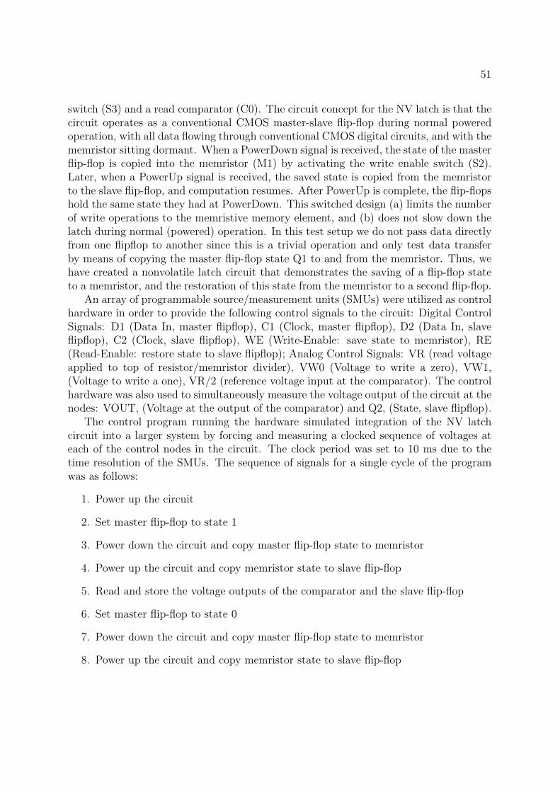
51
switch (S3) and a read comparator (C0). The circuit concept for the NV latch is that thecircuit operates as a conventional CMOS master-slave flip-flop during normal poweredoperation, with all data flowing through conventional CMOS digital circuits, and with thememristor sitting dormant. When a PowerDown signal is received, the state of the masterflip-flop is copied into the memristor (M1) by activating the write enable switch (S2).Later, when a PowerUp signal is received, the saved state is copied from the memristorto the slave flip-flop, and computation resumes. After PowerUp is complete, the flip-flopshold the same state they had at PowerDown. This switched design (a) limits the numberof write operations to the memristive memory element, and (b) does not slow down thelatch during normal (powered) operation. In this test setup we do not pass data directlyfrom one flipflop to another since this is a trivial operation and only test data transferby means of copying the master flip-flop state Q1 to and from the memristor. Thus, wehave created a nonvolatile latch circuit that demonstrates the saving of a flip-flop stateto a memristor, and the restoration of this state from the memristor to a second flip-flop.
An array of programmable source/measurement units (SMUs) were utilized as controlhardware in order to provide the following control signals to the circuit: Digital ControlSignals: D1 (Data In, master flipflop), C1 (Clock, master flipflop), D2 (Data In, slaveflipflop), C2 (Clock, slave flipflop), WE (Write-Enable: save state to memristor), RE(Read-Enable: restore state to slave flipflop); Analog Control Signals: VR (read voltageapplied to top of resistor/memristor divider), VW0 (Voltage to write a zero), VW1,(Voltage to write a one), VR/2 (reference voltage input at the comparator). The controlhardware was also used to simultaneously measure the voltage output of the circuit at thenodes: VOUT, (Voltage at the output of the comparator) and Q2, (State, slave flipflop).
The control program running the hardware simulated integration of the NV latchcircuit into a larger system by forcing and measuring a clocked sequence of voltages ateach of the control nodes in the circuit. The clock period was set to 10 ms due to thetime resolution of the SMUs. The sequence of signals for a single cycle of the programwas as follows:
1. Power up the circuit
2. Set master flip-flop to state 1
3. Power down the circuit and copy master flip-flop state to memristor
4. Power up the circuit and copy memristor state to slave flip-flop
5. Read and store the voltage outputs of the comparator and the slave flip-flop
6. Set master flip-flop to state 0
7. Power down the circuit and copy master flip-flop state to memristor
8. Power up the circuit and copy memristor state to slave flip-flop

52
9. Read and store the voltage outputs of the comparator and the slave flip-flop
This cycle was repeated 2000 times in order to determine the performance of the circuitand the memristor during many operations.
The NV latch circuit operated successfully for 1500 cycles with an error rate less than1%, as shown by the sequence of slave flip-flop outputs in Figure 5.3. As the numberof cycles increased, failure was observed in that the circuit was no longer able to storethe ON state of the master flip-flop through power cycles for the chosen threshold valuesfor ON and OFF. Failure of the memristor after 1500 cycles was a relatively slow andcontinuous event as shown by the progression of the voltage output of the comparator inFigure 5.3. This output slowly increases because the ON state of the memristor steadilybecomes more resistive relative to the voltage divider resistor, causing the divider outputto steadily increase. Failure of laboratory fabricated memristors has previously beenattributed to the failure of nanowire electrodes which could be possibly be improved byoxide passivation, improvements in device planarity, or utilization of refractory metalelectrodes [119].
In summary, we demonstrated that a memristor can be used as a memory elementin a nonvolatile latch circuit. This circuit could be used in a nonvolatile processor. Thefeasibility of the tight integration of memristors with conventional CMOS circuitry wasshown by the recent hybrid memristor/CMOS SNIC chip. In normal powered operationof this circuit, there is no speed penalty, since the memristor is not used for this function.The use of the memristor is limited to the times at which power fails, or is restored. Sincethis circuit was built and tested, the endurance of memristors has been improved to therange of 109 − 1010 write operations which is a figure that enables effectively unlimitedoperation if the power even once a second.
5.2 A defect-tolerant crossbar demultiplexer
Demultiplexer (demux) circuits are needed for interfacing micro- to nano-circuitryin order to electronically access highly integrated nanowire-based circuits. In a demulti-plexer a small number of address wires control a much larger number of nanowires througha selection matrix which must be of roughly the same feature scale as the nanowires in or-der to minimize area overhead. Previously it was been shown that a crossbar of nanowirescan be used as a demultiplexer [120], making it reasonable to envision microscale com-ponents wired to vast crossbars of nanoscale components. As the size of the featuresdecrease it is likely that manufacturing defects in the nano-circuitry will inevitably in-crease, causing the demultiplexer to malfunction under conventional architecture design.To deal with this issue, approaches towards defect tolerant computer architectures havebeen developed theoretically, primary based on coding theory [121]. In this work, we showthe fabrication of a 50 nm half-pitch nanowire crossbar array with electrically switchingtitanium oxide memristors and demonstrate how to reliably address a specific nanowire in

53
Figure 5.3: Circuit test results demonstrating the output voltage of the voltage dividerduring the READ operation after the master FF was in the OFF (a) and ON (b) states.The total number of write errors (c) starts to increase sharply at around 1200 cyclesreaching 1% at around 1500 cycles.

54
a nano-crossbar array with a partially defective nano-crossbar demultiplexer by utilizingthe error-correcting coding theory.
A fully addressable 17 × 17 nano-crossbar circuit at 50 nm half-pitch was designedfor this study. Figure 5.4 shows three microscopic images of the crossbar including anoptical image including the electrode fanout and pads (a) as well as high magnificationAFM (b) and SEM (c) images of the crossbar itself. A sub-array of this crossbar wasused to demonstrate the defect tolerance. The general fabrication process was reportedextensively in previously [107] but is briefly described here. Two sequential steps of UV-based nanoimprint liftoff process produced crossbar arrays fabricated on silicon waferswith a 100 nm thermal oxide overlayer. The first imprint step generated the bottomelectrodes which were composed of 2 nm of Ti and 9 nm of Pt. After the first imprintprocess a blanket layer of TiO2 was prepared by five cycles of 1.5 nm Ti depositionimmediately followed by oxygen plasma exposure in order to create a TiO2 switchingfilm. The top electrode of 2 nm Ti / 9 nm Pt, orthogonal to the bottom electrode,was then fabricated by the second nanoimprint process. After the formation of the topelectrode, the device was subjected to O2/CHF3 plasma in a RIE for 1 min to removethe TiO2 that was not directly under the top electrodes. This step not only exposed thebottom electrode fanouts for ohmic electrical contact, but also reduced the possibility ofcross-talk between neighboring nanowires.
The multilayer TiO2 deposition process described above was designed to exhibit an-tifuse type switching with a large resistance change between the as-grown state and thewritten state. It was written to the low resistance state from its initial insulating stateby applying a voltage of about 3 V and exhibited an on/off ratio of greater than 104. Themultilayer oxide could subsequently be switched off by applying a negative voltage bias,but the following switching event in these films usually has small on/off ratio, typical ofless than 10. This type of behavior is not useful for nonvolatile memory devices, but isvery useful for demultiplexers which only need to be programmed once in the lifetime ofthe circuit.
Although most of the junctions showed reliable switching during the programmingtest, we observed a small fraction of the junctions in the nano-crossbar arrays which couldnot be turned on, a defect know as a “stuck open” defect. In order to deal this somewhatcommon stuck-open defect, we adopted the defect-tolerant approach based on codingtheory which was previously worked out [122, 121] in simulation. The basic purposeof these codes is to convert raw addresses into longer-bit-length codewords such thatthe resulting codewords are substantially different from each other. This “substantialdifference” is quantitatively defined as the minimum number of different bits betweenany two codewords and is referred to as the minimum Hamming distance, denoted as d.In this scheme, a minimum Hamming distance of d allows for d − 1 stuck open defectsper output line in the demultiplexer because it requires d errors to make a mistake whenusing codewords d bits apart. In coding theory nomenclature, the number of bits in thecodeword is typically denoted by n, the number of bits in the original address by k, a setof codes defined by these parameters is denoted as an [n, k, d] code, and the matrix used

55
Encoded Address Lines
Out
put L
ines
A B C D E F A B C D E F
S0S1S2S3S4S5S6S7
(a) (b)
(c)
Figure 5.4: Optical (a), atomic force (b), and scanning electron (c) micrographs of a50×50 nm2 17×17 memristor crossbar used to demonstrate a defect tolerant resistorlogic demultiplexer. The crossbar columns were used for the balance input address whichselected a single output row.

56
A B C D E F A B C D E F
S0S1S2S3S4S5S6S7
OutputLines
EncodedAddressLines
ProgrammedCrosspoint
Figure 5.5: Schematic of the ideally programmed demultiplexer with conductive cross-points indicated by the blue dots. As discussed in the text, the error correcting codesused here allow each output line to contain a maximum of two errors while still operatingcorrectly.
to generate the codewords is denoted by g.For experimental characterization of the defect-tolerant demultiplexer on our nano-
crossbar devices, we generated a [6, 3, 3] code and laid it out on a 12×8 crossbar sub-arrayfor selecting an output line when its respective encoded address (a codeword) is input.The generating matrix that we used was:
g =
1 0 0 1 1 00 1 0 1 0 10 0 1 0 1 1
(5.1)

57
which resulted in the generation of the following set of codewords:
c0 = 0 0 0 0 0 0c1 = 0 0 1 0 1 1c2 = 0 1 0 1 0 1c3 = 0 1 1 1 1 0c4 = 1 0 0 1 1 0c5 = 1 0 1 1 0 1c6 = 1 1 0 0 1 1c7 = 1 1 1 0 0 0
(5.2)
The codewords were balanced by taking their complement and appending it to the code-word. This set of balanced codewords was then programmed into the crossbar in orderto enable each line to be selected when the appropriate codeword is input at the addresslines. A schematic of the ideally programmed demultiplexer is shown in Figure 5.5. Sincethe Hamming distance, d, of this code is 3 the demultiplexer should be able to tolerateup to two defects per line.
The crossbar was contacted with a probe card and initially tested for nanowire con-tinuity and shorts between nanowires to rule out the other defects. Typical resistancesof the nanowires from end to end was about 40 kΩ. After a suitable 12 × 8 nano-crossbar sub-array with good nanowires was identified, the desired crossbar junctionswere programmed by applying a switching bias of 4.5-6V across the junctions. Duringthe programming process we formed two different configurations, one with≤ 3 stuck-opendefects per line and one with ≤ 2 defects per line. A map of the programmed crossbarresistance states measured at low bias of 0.5V for both configurations is shown in Figure5.6. The junctions were considered to be switched ‘ON’ if the resistance was less than20 MΩ , whereas the junctions were consider to be un-programmed or stuck-open if theresistance was greater than 500 MΩ.
After programming the demultiplexer configurations, we tested their ability to selectthe proper output line in the presence of the intentional defects. The device was againcontacted with the probe card and was tested by applying all of the codewords to thecrossbars with a logical 1 (bias of 1 V) and logical 0 (bias of 0 V). The application ofone volt did not cause the resistance of the switches to change significantly. When eachcodeword was applied we recorded the voltage on each output line to see the output bias.The results of the test showed that the demultiplexer worked as expected from previoustheoretical analysis. As shown in Figure 5.7 (a), the demultiplexer with ≤3 stuck-opendefects per line had a high output on the appropriate output line for each input code.However there are also two erroneous output lines selected when they are not supposedto be, including line seven for code 000000 and line two for code 101101. These errorsare consistent with the model because lines seven and two are the ones that contain 3defects as shown in Figure 5.6. The demultiplexer programmed with ≤2 defects per line(Figure 5.7 (b)) selects all of the correct lines and does not select any incorrect lines. Thevoltage margin between selected and unselected lines was measured to be 0.2 V under

58
0
1
2
3
4
5
6
7
Ou
tpu
t L
ines
FEDCBAFEDCBA
Encoded Address Lines
50
40
30
20
10
Jun
ction
Resistan
ce (MW
)
(b)
0
1
2
3
4
5
6
7
Ou
tpu
t L
ines
FEDCBAFEDCBA
Encoded Address Lines
50
40
30
20
10
Jun
ction
Resistan
ce (MW
)
(c)
0
1
2
3
4
5
6
7
Ou
tpu
t L
ines
FEDCBAFEDCBA
Encoded Address Lines
(a)
Figure 5.6: Ideally programmed (a) map of the junction resistance where dark cross-points indicate the programmed or conductive state. Maps of the junction resistance as-programmed into the crossbar demultiplexer for (b) ≤ 3 errors per output line and (c) ≤2 errors per output line. Intentionally introduced errors in the demux programming areindicted by the red circles.

59
000000
001011
010101
011110
100110
101101
110011
111000
En
cod
ed A
dd
ress
0 1 2 3 4 5 6 7
Output Lines
1.0
0.8
0.6
0.4
0.2
0.0
Ou
tpu
t Lin
e Vo
ltage (V
)000000
001011
010101
011110
100110
101101
110011
111000
En
cod
ed A
dd
ress
0 1 2 3 4 5 6 7
Output Lines
1.0
0.8
0.6
0.4
0.2
0.0
Ou
tpu
t Lin
e Vo
ltage (V
)(a)
(b)
Figure 5.7: Output line selection maps for the ≤ 3 (a) and the ≤ 2 (b) as-programmedstates of the crossbar demux. These plots indicate the output voltage on each line for eachencoded address generated by the coding scheme. As expected, in the leq 3 configurationoutput lines 2 and 7 are erroneously selected because they contain 3 errors. the ≤ 2configuration selects all output lines correctly.

60
1.0
0.8
0.6
0.4
0.2
0.0
Ou
tpu
t V
olt
ages
(V
)
1.51.00.50.0Input Bias (V)
Figure 5.8: The margin between selected and unselected output lines for a resistor logicdemultiplexer is a function of the input voltage placed on the address lines. As thevoltage increases, the absolute margin also increases.
the current input level of 1 V, which is well above the noise floor of the measurementsystem.
In order to determine the margin as a function of input bias, the nano-crossbar de-multiplexer with up to two-defect configuration in Figure 5.7 (b) was tested at 0.5 V,0.75 V, and 1 V, respectively. The results, shown in Figure 5.8, demonstrate that themargin increases with increasing applied voltage for our crossbar demultiplexer device. Itis worth to note that even though the margin increased slightly at 1 V input, the voltageson the selected wires are also more scattered than that tested at 0.5 and 0.75 V. Thismay be attributed to the non-linearity of the i− v characteristics of the titanium dioxidejunctions, at higher input voltage the junction resistance will decrease and cause morepotential sneaking current path inside the resistor-only cross-bar array. Further improve-ment of the switching characteristics of the oxide junction as well as the incorporation ofdiode-like behavior into the junction will likely to provide more stable demultiplexer oper-ation. Nevertheless, this first physical demonstration of defect-tolerant demultiplexer willbe useful in designing nano-crossbar circuits for addressing other nano-crossbar memory,logic, routing circuits as well as nanowire-based sensor arrays.

61
Bibliography
[1] T. W. Hickmott, “Low-frequency negative resistance in thin anodic oxide films,”Journal of Applied Physics, vol. 33, no. 9, pp. 2669–2682, 1962.
[2] W. R. Hiatt and T. W. Hickmott, “Bistable switching in niobium oxide diodes,”Applied Physics Letters, vol. 6, no. 6, pp. 106–108, 1965.
[3] J. F. Gibbons and W. E. Beadle, “Switching properties of thin NiO films,” Solid-State Electronics, vol. 7, no. 11, pp. 785–790, 1964.
[4] G. Dearnaley, A. M. Stoneham, and D. V. Morgan, “Electrical phenomena in amor-phous oxide films,” Reports on Progress in Physics, vol. 33, no. 3, pp. 1129–1191,1970.
[5] J. G. Simmons, “Conduction in thin dielectric films,” Journal of Physics D: AppliedPhysics, vol. 4, no. 5, pp. 613–657, 1971.
[6] D. Frohman-Bentchkowsky, “Memory behavior in a floating-gate avalanche-injection MOS (FAMOS) structure,” Applied Physics Letters, vol. 18, no. 8,pp. 332–334, 1971.
[7] D. Frohman-Bentchkowsky, “A fully decoded 2048-bit electrically programmableFAMOS read-only memory,” Solid-State Circuits, IEEE Journal of, vol. 6, no. 5,pp. 301–306, 1971.
[8] Y. Watanabe, “Reproducible memory effect in the leakage current of epitaxial fer-roelectric/conductive perovskite heterostructures,” Applied Physics Letters, vol. 66,no. 1, pp. 28–30, 1995.
[9] J. Rodrıguez Contreras, H. Kohlstedt, U. Poppe, R. Waser, C. Buchal, andN. A. Pertsev, “Resistive switching in metal–ferroelectric–metal junctions,” Ap-plied Physics Letters, vol. 83, no. 22, pp. 4595–4597, 2003.
[10] A. Beck, J. G. Bednorz, C. Gerber, C. Rossel, and D. Widmer, “Reproducibleswitching effect in thin oxide films for memory applications,” Applied Physics Let-ters, vol. 77, no. 1, pp. 139–141, 2000.

62
[11] Y. Watanabe, J. G. Bednorz, A. Bietsch, C. Gerber, D. Widmer, A. Beck, and S. J.Wind, “Current-driven insulator-conductor transition and nonvolatile memory inchromium-doped SrTiO3 single crystals,” Applied Physics Letters, vol. 78, no. 23,pp. 3738–3740, 2001.
[12] S. Q. Liu, N. J. Wu, and A. Ignatiev, “Electric-pulse-induced reversible resistancechange effect in magnetoresistive films,” Applied Physics Letters, vol. 76, no. 19,pp. 2749–2751, 2000.
[13] A. Baikalov, Y. Q. Wang, B. Shen, B. Lorenz, S. Tsui, Y. Y. Sun, Y. Y. Xue,and C. W. Chu, “Field-driven hysteretic and reversible resistive switch at theAg–Pr0.7Ca0.3MnO3 interface,” Applied Physics Letters, vol. 83, no. 5, pp. 957–959, 2003.
[14] N. Melosh, A. Boukai, F. Diana, B. Gerardot, A. Badolato, P. Petroff, and J. Heath,“Ultrahigh-density nanowire lattices and circuits,” Science, vol. 300, no. 5616,pp. 112–115, 2003.
[15] Y. Chen, G.-Y. Jung, D. Ohlberg, X. Li, D. Stewart, J. Jeppesen, K. Nielsen,F. Stoddart, and R. S. Williams, “Nanoscale molecular-switch crossbar circuits,”Nanotechnology, vol. 14, no. 4, pp. 462–468, 2003.
[16] J. Heath, P. Kuekes, G. Snider, and R. S. Williams, “A defect-tolerant com-puter architecture: Opportunities for nanotechnology,” Science, vol. 280, no. 5370,pp. 1716–1721, 1998.
[17] O. Turel and K. Likharev, “Crossnets: possible neuromorphic networks based onnanoscale components,” International Journal of Circuit Theory and Applications,vol. 31, no. 1, pp. 37–53, 2003.
[18] D. Strukov and K. Likharev, “Prospects for terabit-scale nanoelectronic memories,”Nanotechnology, vol. 16, no. 1, pp. 137–148, 2005.
[19] K. Szot, W. Speier, G. Bihlmayer, and R. Waser, “Switching the electrical re-sistance of individual dislocations in single-crystalline SrTiO3,” Nature Materials,vol. 5, no. 4, pp. 312–320, 2006.
[20] “Emerging research devices,” tech. rep., International Technology Roadmap forSemiconductors, 2009.
[21] C. Rossel, G. I. Meijer, D. Bremaud, and D. Widmer, “Electrical current distribu-tion across a metal-insulator-metal structure during bistable switching,” Journalof Applied Physics, vol. 90, no. 6, pp. 2892–2898, 2001.
63
[22] B. J. Choi, D. S. Jeong, S. K. Kim, C. Rohde, S. Choi, J. H. Oh, H. J. Kim, C. S.Hwang, K. Szot, R. Waser, B. Reichenberg, and S. Tiedke, “Resistive switchingmechanism of TiO2 thin films grown by atomic-layer deposition,” Journal of AppliedPhysics, vol. 98, no. 3, 2005.
[23] D. Jeong, H. Schroeder, and R. Waser, “Impedance spectroscopy of TiO2 thin filmsshowing resistive switching,” Applied Physics Letters, vol. 89, no. 8, 2006.
[24] M. Janousch, G. I. Meijer, U. Staub, B. Delley, S. F. Karg, and B. P. Andreasson,“Role of oxygen vacancies in Cr–doped SrTiO3 for resistance-change memory,”Advanced Materials, vol. 19, no. 17, pp. 2232–2235, 2007.
[25] K. M. Kim, B. J. Choi, and C. S. Hwang, “Localized switching mechanism in resis-tive switching of atomic-layer-deposited TiO2 thin films,” Applied Physics Letters,vol. 90, no. 24, pp. 242906–3, 2007.
[26] Y. Sato, K. Kinoshita, M. Aoki, and Y. Sugiyama, “Consideration of switch-ing mechanism of binary metal oxide resistive junctions using a thermal reactionmodel,” Applied Physics Letters, vol. 90, no. 3, 2007.
[27] S. Chae, J. Lee, S. Kim, S. Lee, S. Chang, C. Liu, B. Kahng, H. Shin, D.-W. Kim,C. Jung, S. Seo, M.-J. Lee, and T. Noh, “Random circuit breaker network model forunipolar resistance switching,” Advanced Materials, vol. 20, no. 6, pp. 1154–1159,2008.
[28] J. Yang, F. Miao, M. D. Pickett, D. Ohlberg, D. Stewart, C. Lau, and R. S.Williams, “The mechanism of electroforming of metal oxide memristive switches,”Nanotechnology, vol. 20, no. 21, p. 215201, 2009.
[29] J. P. Strachan, J. J. Yang, R. Mnstermann, A. Scholl, G. Medeiros-Ribeiro,D. R. Stewart, and R. S. Williams, “Structural and chemical characterization ofTiO2 memristive devices by spatially-resolved NEXAFS,” Nanotechnology, vol. 20,no. 48, p. 485701, 2009.
[30] D.-H. Kwon, K. Kim, J. Jang, J. Jeon, M. Lee, G. Kim, X.-S. Li, G.-S. Park, B. Lee,S. Han, M. Kim, and C. Hwang, “Atomic structure of conducting nanofilaments inTiO2 resistive switching memory,” Nature Nanotechnology, vol. 5, no. 2, pp. 148–153, 2010.
[31] J. P. Strachan, M. D. Pickett, J. Yang, S. Aloni, D. Kilcoyne, G. Medeiros-Ribeiro,and R. S. Williams, “Direct identification of the conducting channels in a func-tioning memristive device,” Advanced Materials, vol. 22, no. 32, pp. 3573–3577,2010.

64
[32] M. Fujimoto, H. Koyama, M. Konagai, Y. Hosoi, K. Ishihara, S. Ohnishi, andN. Awaya, “TiO2 anatase nanolayer on TiN thin film exhibiting high-speed bipolarresistive switching,” Applied Physics Letters, vol. 89, no. 22, 2006.
[33] S. Karg, G. I. Meijer, D. Widmer, and J. G. Bednorz, “Electrical-stress-inducedconductivity increase in SrTiO3 films,” Applied Physics Letters, vol. 89, no. 7,p. 072106, 2006.
[34] T. Fujii, M. Kawasaki, A. Sawa, Y. Kawazoe, H. Akoh, and Y. Tokura,“Electrical properties and colossal electroresistance of heteroepitaxialSrRuO3/SrTi1−xNbxO3(0.0002 ≤ x ≤ 0.02) schottky junctions,” PhysicalReview B, vol. 75, no. 16, p. 165101, 2007.
[35] J. Jameson, Y. Fukuzumi, Z. Wang, P. Griffin, K. Tsunoda, I. Meijer, and Y. Nishi,“Field-programmable rectification in rutile TiO2 crystals,” Applied Physics Letters,vol. 91, no. 11, 2007.
[36] S. Hirose, A. Nakayama, H. Niimi, K. Kageyama, and H. Takagi, “Resistanceswitching and retention behaviors in polycrystalline La-doped SrTiO3 ceramicschip devices,” Journal of Applied Physics, vol. 104, no. 5, pp. 053712–12, 2008.
[37] B. Phan and J. Lee, “Effects of interfacial oxygen-deficient layer on resistanceswitching in Cr-doped SrTiO3 thin films,” Applied Physics Letters, vol. 93, no. 22,2008.
[38] M. Hasan, R. Dong, H. J. Choi, D. S. Lee, D. J. Seong, M. B. Pyun, and H. Hwang,“Uniform resistive switching with a thin reactive metal interface layer in metal-La0.7Ca0.3MnO3-metal heterostructures,” Applied Physics Letters, vol. 92, no. 20,pp. 202102–3, 2008.
[39] D. Jeong, H. Schroeder, U. Breuer, and R. Waser, “Characteristic electroform-ing behavior in Pt/TiO2/Pt resistive switching cells depending on atmosphere,”Journal of Applied Physics, vol. 104, no. 12, 2008.
[40] C. H. Yang, J. Seidel, S. Y. Kim, P. B. Rossen, P. Yu, M. Gajek, Y. H. Chu,L. W. Martin, M. B. Holcomb, Q. He, P. Maksymovych, N. Balke, S. V. Kalinin,A. P. Baddorf, S. R. Basu, M. L. Scullin, and R. Ramesh, “Electric modulation ofconduction in multiferroic Ca-doped BiFeO3 films,” Nature Materials, vol. 8, no. 6,pp. 485–493, 2009.
[41] D. Strukov, G. Snider, D. Stewart, and R. S. Williams, “The missing memristorfound,” Nature, vol. 453, no. 7191, pp. 80–83, 2008.
[42] L. Chua, “Memristor-the missing circuit element,” IEEE Transactions on CircuitTheory, vol. 18, no. 5, pp. 507–519, 1971.

65
[43] D. Strukov and R. S. Williams, “Exponential ionic drift: fast switching and lowvolatility ofthin-film memristors,” Applied Physics A: Materials Science & Process-ing, vol. 94, pp. 515–519, 2008.
[44] D. Strukov, J. Borghetti, and R. S. Williams, “Coupled ionic and electronic trans-port model of thin-film semiconductor memristive behavior,” Small, vol. 5, no. 9,pp. 1058–1063, 2009.
[45] D. Jeong, H. Schroeder, and R. Waser, “Mechanism for bipolar switching in aPt/TiO2/Pt resistive switching cell,” Physical Review B, vol. 79, no. 19, p. 195317,2009.
[46] A. Sawa, T. Fujii, M. Kawasaki, and Y. Tokura, “Hysteretic current–voltage char-acteristics and resistance switching at a rectifying Ti/Pr0.7Ca0.3MnO3 interface,”Applied Physics Letters, vol. 85, no. 18, pp. 4073–4075, 2004.
[47] T. Fujii, M. Kawasaki, A. Sawa, H. Akoh, Y. Kawazoe, and Y. Tokura, “Hystereticcurrent–voltage characteristics and resistance switching at an epitaxial oxide schot-tky junction SrRuO3/SrTi0.99Nb0.01O3,” Applied Physics Letters, vol. 86, no. 1,2005.
[48] Y. Tokunaga, Y. Kaneko, J. P. He, T. Arima, A. Sawa, T. Fujii, M. Kawasaki, andY. Tokura, “Colossal electroresistance effect at metal electrode/La1−xSr1+xMnO4
interfaces,” Applied Physics Letters, vol. 88, no. 22, pp. 223507–3, 2006.
[49] S. Hirose, H. Nishimura, and H. Niimi, “Resistance switching effect in Nb-dopedSrTiO3 (100) bicrystal with (100) ∼ 45 degree twist boundary,” Journal of AppliedPhysics, vol. 106, no. 4, p. 043714, 2009.
[50] J. Yang, M. D. Pickett, X. Li, D. Ohlberg, D. Stewart, and R. S. Williams, “Memris-tive switching mechanism for metal/oxide/metal nanodevices,” Nature Nanotech-nology, vol. 3, no. 7, pp. 429–433, 2008.
[51] F. Miao, J. J. Yang, J. P. Strachan, D. Stewart, R. S. Williams, and C. N. Lau,“Force modulation of tunnel gaps in metal oxide memristive nanoswitches,” AppliedPhysics Letters, vol. 95, no. 11, pp. 113503–3, 2009.
[52] J. Borghetti, D. B. Strukov, M. D. Pickett, J. J. Yang, D. R. Stewart, and R. S.Williams, “Electrical transport and thermometry of electroformed titanium dioxidememristive switches,” Journal of Applied Physics, vol. 106, no. 12, pp. 124504–5,2009.
[53] M. D. Pickett, D. Strukov, J. Borghetti, J. Yang, G. Snider, D. Stewart, and R. S.Williams, “Switching dynamics in titanium dioxide memristive devices,” Journalof Applied Physics, vol. 106, no. 7, p. 074508, 2009.

66
[54] M. D. Pickett, J. Borghetti, J. J. Yang, G. Medeiros-Ribeiro, and R. S. Williams,“Coexistence of memristance and negative differential resistance in a nanoscalemetal-oxide-metal system,” Submitted, 2010.
[55] Z. Li, M. D. Pickett, D. Stewart, D. Ohlberg, X. Li, W. Wu, W. Robinett, andR. S. Williams, “Experimental demonstration of a defect-tolerant nanocrossbardemultiplexer,” Nanotechnology, vol. 19, no. 16, p. 165203, 2008.
[56] W. Robinett, M. D. Pickett, J. Borghetti, Q. Xia, G. S. Snider, G. Medeiros-Ribeiro,and R. S. Williams, “A memristor-based nonvolatile latch circuit,” Nanotechnology,vol. 21, no. 23, p. 235203, 2010.
[57] R. Waser and M. Aono, “Nanoionics-based resistive switching memories,” NatureMaterials, vol. 6, no. 11, pp. 833–840, 2007.
[58] R. Waser, R. Dittmann, G. Staikov, and K. Szot, “Redox-based resistive switchingmemories - nanoionic mechanisms, prospects, and challenges,” Advanced Materials,vol. 21, no. 25-26, pp. 2632–2663, 2009.
[59] A. Odagawa, H. Sato, I. H. Inoue, H. Akoh, M. Kawasaki, Y. Tokura, T. Kanno,and H. Adachi, “Colossal electroresistance of a Pr0.7Ca0.3MnO3 thin film at roomtemperature,” Physical Review B, vol. 70, no. 22, 2004.
[60] M. J. Rozenberg, I. H. Inoue, and M. J. Sanchez, “Nonvolatile memory withmultilevel switching: A basic model,” Physical Review Letters, vol. 92, no. 17,pp. 178302–1, 2004.
[61] A. L. D. Kilcoyne, T. Tyliszczak, W. F. Steele, S. Fakra, P. Hitchcock, K. Franck,E. Anderson, B. Harteneck, E. G. Rightor, G. E. Mitchell, A. P. Hitchcock, L. Yang,T. Warwick, and H. Ade, “Interferometer-controlled scanning transmission x-raymicroscopes at the advanced light source,” Journal of Synchrotron Radiation,vol. 10, no. 2, pp. 125–136, 2003.
[62] G. van der Laan, “Polaronic satellites in x-ray-absorption spectra,” Physical ReviewB, vol. 41, no. 17, p. 12366, 1990.
[63] F. M. F. de Groot, J. C. Fuggle, B. T. Thole, and G. A. Sawatzky, “2p x-rayabsorption of 3d transition-metal compounds: An atomic multiplet descriptionincluding the crystal field,” Physical Review B, vol. 42, no. 9, p. 5459, 1990.
[64] F. M. F. de Groot, M. O. Figueiredo, M. J. Basto, M. Abbate, H. Petersen, andJ. C. Fuggle, “2p x-ray absorption of titanium in minerals,” Physics and Chemistryof Minerals, vol. 19, no. 3, pp. 140–147, 1992.

67
[65] M. Abbate, F. M. F. de Groot, J. C. Fuggle, A. Fujimori, Y. Tokura, Y. Fujishima,O. Strebel, M. Domke, G. Kaindl, J. van Elp, B. T. Thole, G. A. Sawatzky, M. Sac-chi, and N. Tsuda, “Soft-x-ray-absorption studies of the location of extra chargesinduced by substitution in controlled-valence materials,” Physical Review B, vol. 44,no. 11, p. 5419, 1991.
[66] E. Stoyanov, F. Langenhorst, and G. Steinle-Neumann, “The effect of valence stateand site geometry on Ti L3,2 and O K electron energy-loss spectra of TixOy phases,”American Mineralogist, vol. 92, no. 4, pp. 577–586, 2007.
[67] A. Ohtomo, D. A. Muller, J. L. Grazul, and H. Y. Hwang, “Epitaxial growthand electronic structure of LaTiOx films,” Applied Physics Letters, vol. 80, no. 21,pp. 3922–3924, 2002.
[68] L. Soriano, M. Abbate, J. Vogel, J. C. Fuggle, A. Fernandez, A. R. Gonzalez-Elipe,M. Sacchi, and J. M. Sanz, “Chemical changes induced by sputtering in TiO2
and some selected titanates as observed by x-ray absorption spectroscopy,” SurfaceScience, vol. 290, no. 3, pp. 427–435, 1993.
[69] V. S. Lusvardi, M. A. Barteau, J. G. Chen, J. Eng, B. Fruhberger, andA. Teplyakov, “An NEXAFS investigation of the reduction and reoxidation of TiO2
(001),” Surface Science, vol. 397, no. 1-3, pp. 237–250, 1998.
[70] M. Marezio, “The crystal structure of Ti4O7, a member of the homologous seriesTinO2n−1,” Journal of Solid State Chemistry, vol. 3, no. 3, pp. 340–348, 1971.
[71] R. Bartholomew and D. R. Frankl, “Electrical properties of some titanium oxides,”Physical Review, vol. 187, no. 3, pp. 828–833, 1969.
[72] L. Liborio and N. Harrison, “Thermodynamics of oxygen defective Magneli phasesin rutile: A first-principles study,” Physical Review B, vol. 77, no. 10, p. 104104,2008.
[73] R. Meyer, R. Liedtke, and R. Waser, “Oxygen vacancy migration and time-dependent leakage current behavior of Ba0.3Sr0.7TiO3 thin films,” Applied PhysicsLetters, vol. 86, no. 11, p. 112904, 2005.
[74] R. Meyer, L. Schloss, J. Brewer, R. Lambertson, W. Kinney, J. Sanchez, andD. Rinerson, “Oxide dual-layer memory element for scalable non-volatile cross-point memory technology,” in Non-Volatile Memory Technology Symposium, 2008.NVMTS 2008. 9th Annual, pp. 1–5, 2008.
[75] L. Chua and S. Kang, “Memristive devices and systems,” Proceedings of the IEEE,vol. 64, no. 2, pp. 209–223, 1976.

68
[76] J. Simmons, “Generalized formula for the electric tunnel effect between similarelectrodes separated by a thin insulating film,” Journal of Applied Physics, vol. 34,no. 6, pp. 1793–1803, 1963.
[77] P. Boggs, J. Donaldson, R. Byrd, and R. Schnabel, “Algorithm 676: ODRPACK:software for weighted orthogonal distance regression,” ACM Transactions on Math-ematical Software, vol. 15, no. 4, pp. 348–364, 1989.
[78] H. Tang, K. Prasad, R. Sanjines, P. E. Schmid, and F. Levy, “Electrical and opticalproperties of TiO2 anatase thin films,” Journal of Applied Physics, vol. 75, no. 4,pp. 2042–2047, 1994.
[79] A. D. Inglis, L. Page, P. Strobel, and C. M. Hurd, “Electrical conductance ofcrystalline TinO2n−1 for n=4-9,” Journal of Physics C: Solid State Physics, vol. 16,no. 2, pp. 317–333, 1983.
[80] N. Mott and R. W. Gurney, Electronic Processes in Ionic Crystals. Dover, 1964.
[81] T. Tamura, T. Hasegawa, K. Terabe, T. Nakayama, T. Sakamoto, H. Sunamura,H. Kawaura, S. Hosaka, and M. Aono, “Material dependence of switching speedof atomic switches made from silver sulfide and from copper sulfide,” Journal ofPhysics: Conference Series, vol. 61, no. 1, p. 1157, 2007.
[82] J. G. Simmons and R. R. Verderber, “New conduction and reversible memoryphenomena in thin insulating films,” Proceedings of the Royal Society of London.Series A, Mathematical and Physical Sciences (1934-1990), vol. 301, no. 1464,pp. 77–102, 1967.
[83] H. Pagnia and N. Sotnik, “Bistable switching in electroformed metal-insulator-metal devices,” Physica Status Solidi (a), vol. 108, no. 1, pp. 11–65, 1988.
[84] S. Andersson, B. Colln, U. Kuylenstierna, and A. Magnli, “Phase analysis studieson the titanium-oxygen system,” Acta Chemica Scandinavica, vol. 11, pp. 1641–1652, 1957.
[85] H. Futaki, “A new type semiconductor (critical temperature resistor),” JapaneseJournal of Applied Physics, vol. 4, no. 1, pp. 28–41, 1965.
[86] R. G. Cope and A. W. Penn, “High-speed solid-state thermal switches based onvanadium dioxide,” Journal of Physics D: Applied Physics, vol. 1, no. 2, p. 161,1968.
[87] C. N. Berglund, “Thermal filaments in vanadium dioxide,” IEEE Transactions onElectron Devices, vol. 16, no. 5, 1969.

69
[88] J. Duchene, M. Terraillon, P. Pailly, and G. Adam, “Filamentary conduction in VO2
coplanar thin-film devices,” Applied Physics Letters, vol. 19, no. 4, pp. 115–117,1971.
[89] H. T. Kim, B. J. Kim, S. Choi, B. G. Chae, Y. W. Lee, T. Driscoll, M. M. Qazilbash,and D. N. Basov, “Electrical oscillations induced by the metal-insulator transitionin VO2,” Journal of Applied Physics, vol. 107, no. 2, 2010.
[90] K. L. Chopra, “Current-controlled negative resistance in thin niobium oxide films,”Proceedings of the IEEE, vol. 51, no. 6, pp. 941–942, 1963.
[91] D. V. Geppert, “A new negative-resistance device,” Proceedings of the IEEE,vol. 51, no. 1, pp. 223–223, 1963.
[92] K. L. Chopra, “Avalanche-induced negative resistance in thin oxide films,” Journalof Applied Physics, vol. 36, no. 1, pp. 184–187, 1965.
[93] F. Argall, “Switching phenomena in titanium oxide thin films,” Solid-State Elec-tronics, vol. 11, no. 5, pp. 535–541, 1968.
[94] R. J. Soukup, “Observations of negative resistance in Ti-TiO2-Au diodes,” Journalof Applied Physics, vol. 43, no. 8, pp. 3431–3435, 1972.
[95] G. Taylor and B. Lalevic, “Threshold switching in polycrystalline TiO2 thin films,”Journal of Applied Physics, vol. 48, no. 10, pp. 4410–4412, 1977.
[96] R. C. Morris, J. E. Christopher, and R. V. Coleman, “Conduction phenomena inthin layers of iron oxide,” Physical Review, vol. 184, no. 2, pp. 565–573, 1969.
[97] F. A. Chudnovskii, L. L. Odynets, A. L. Pergament, and G. B. Stefanovich, “Elec-troforming and switching in oxides of transition metals: The role of metal-insulatortransition in the switching mechanism,” Journal of Solid State Chemistry, vol. 122,no. 1, pp. 95–99, 1996.
[98] J. Kim, C. Ko, A. Frenzel, S. Ramanathan, and J. E. Hoffman, “Nanoscale imagingand control of resistance switching in VO2 at room temperature,” Applied PhysicsLetters, vol. 96, no. 21, p. 213106, 2010.
[99] M. Imada, A. Fujimori, and Y. Tokura, “Metal-insulator transitions,” Reviews ofModern Physics, vol. 70, no. 4, pp. 1039–1263, 1998.
[100] B. K. Ridley, “Specific negative resistance in solids,” Proceedings of the PhysicalSociety, vol. 82, no. 6, p. 954, 1963.

70
[101] S. Lakkis, C. Schlenker, B. K. Chakraverty, R. Buder, and M. Marezio, “Metal-insulator transitions in Ti4O7 single crystals: Crystal characterization, specific heat,and electron paramagnetic resonance,” Physical Review B, vol. 14, no. 4, pp. 1429–1440, 1976.
[102] S. A. Campbell, H. S. Kim, D. C. Gilmer, B. He, T. Ma, and W. L. Gladfelter,“Titanium dioxide (TiO2)-based gate insulators,” IBM Journal of Research andDevelopment, vol. 43, no. 3, pp. 383–392, 1999.
[103] R. Fowler and L. Nordheim, “Electron emission in intense electric fields,” Proceed-ings of the Royal Society of London. Series A, Mathematical and Physical Sciences(1934-1990), vol. 119, pp. 173–181, 1928.
[104] R. Corless, G. Gonnet, D. Hare, D. Jeffrey, and D. Knuth, “On the Lambert Wfunction,” Advances in Computational Mathematics, vol. 5, no. 1, pp. 329–359,1996.
[105] S. M. Lee, D. G. Cahill, and T. H. Allen, “Thermal conductivity of sputtered oxidefilms,” Physical Review B, vol. 52, no. 1, p. 253, 1995.
[106] M. P. Shaw, H. L. Grubin, and I. J. Gastman, “Analysis of an inhomogeneousbulk “S-shaped” negative differential conductivity element in a circuit containingreactive elements,” IEEE Transactions on Electron Devices, vol. 20, no. 2, pp. 169–178, 1973.
[107] W. Wu, G. Y. Jung, D. L. Olynick, J. Straznicky, Z. Li, X. Li, D. A. A. Ohlberg,Y. Chen, S. Y. Wang, J. A. Liddle, W. M. Tong, and R. S. Williams, “One-kilobitcross-bar molecular memory circuits at 30-nm half-pitch fabricated by nanoimprintlithography,” Applied Physics A: Materials Science & Processing, vol. 80, no. 6,pp. 1173–1178, 2005.
[108] Q. Xia, W. Robinett, M. Cumbie, N. Banerjee, T. Cardinali, J. Yang, W. Wu,X. Li, W. Tong, D. Strukov, G. Snider, G. Medeiros-Ribeiro, and R. S. Williams,“Memristor-CMOS hybrid integrated circuits for reconfigurable logic,” Nano Let-ters, vol. 9, no. 10, pp. 3640–3645, 2009.
[109] D. B. Strukov and R. S. Williams, “Four-dimensional address topology for circuitswith stacked multilayer crossbar arrays,” Proceedings of the National Academy ofSciences, vol. 106, no. 48, pp. 20155–20158, 2009.
[110] D. Strukov and K. Likharev, “CMOL FPGA: a reconfigurable architecture forhybrid digital circuits with two-terminal nanodevices,” Nanotechnology, vol. 16,no. 6, pp. 888–900, 2005.
[111] G. Snider and R. S. Williams, “Nano/CMOS architectures using a field-programmable nanowire interconnect,” Nanotechnology, vol. 18, no. 3, 2007.

71
[112] J. Borghetti, Z. Li, J. Straznicky, X. Li, D. A. A. Ohlberg, W. Wu, D. R. Stew-art, and R. S. Williams, “A hybrid nanomemristor/transistor logic circuit capableof self-programming,” Proceedings of the National Academy of Sciences, vol. 106,no. 6, pp. 1699–1703, 2009.
[113] J. Borghetti, G. S. Snider, P. J. Kuekes, J. J. Yang, D. R. Stewart, and R. S.Williams, “‘Memristive’ switches enable ‘stateful’ logic operations via material im-plication,” Nature, vol. 464, no. 7290, pp. 873–876, 2010.
[114] G. S. Snider, “Self-organized computation with unreliable, memristive nanode-vices,” Nanotechnology, vol. 18, no. 36, p. 365202, 2007.
[115] S. H. Jo, T. Chang, I. Ebong, B. B. Bhadviya, P. Mazumder, and W. Lu, “Nanoscalememristor device as synapse in neuromorphic systems,” Nano Letters, vol. 10, no. 4,pp. 1297–1301, 2010.
[116] H. Choi, H. Jung, J. Lee, J. Yoon, J. Park, D.-j. Seong, W. Lee, M. Hasan, G.-Y. Jung, and H. Hwang, “An electrically modifiable synapse array of resistiveswitching memory,” Nanotechnology, vol. 20, no. 34, p. 345201, 2009.
[117] M. Wuttig and N. Yamada, “Phase-change materials for rewriteable data storage,”Nature Materials, vol. 6, no. 11, pp. 824–832, 2007.
[118] S. H. Jo and W. Lu, “CMOS compatible nanoscale nonvolatile resistance switchingmemory,” Nano Letters, 2008.
[119] W. Shen, R. Dittmann, U. Breuer, and R. Waser, “Improved endurance behaviorof resistive switching in (Ba,Sr)TiO3 thin films with W top electrode,” AppliedPhysics Letters, vol. 93, no. 22, p. 222102, 2008.
[120] R. Beckman, E. Johnston-Halperin, Y. Luo, J. Green, and J. Heath, “Bridgingdimensions: Demultiplexing ultrahigh-density nanowire circuits,” Science, vol. 310,no. 5747, pp. 465–468, 2005.
[121] P. J. Kuekes, W. Robinett, and R. S. Williams, “Defect tolerance in resistor-logicdemultiplexers for nanoelectronics,” Nanotechnology, vol. 17, no. 10, p. 2466, 2006.
[122] P. J. Kuekes, W. Robinett, G. Seroussi, and R. S. Williams, “Defect-tolerant inter-connect to nanoelectronic circuits: internally redundant demultiplexers based onerror-correcting codes,” Nanotechnology, vol. 16, no. 6, p. 869, 2005.