the last mile: moving 3d ic into hvm e. jan vardaman president · ctea2105 © 2015 techsearch...
TRANSCRIPT

CTEA2105 © 2015 TechSearch International, Inc.
The Last Mile: Moving 3D IC into HVM
E. Jan Vardaman President
TechSearch International, Inc.
www.techsearchinc.com
CTEA2105 © 2015 TechSearch International, Inc.
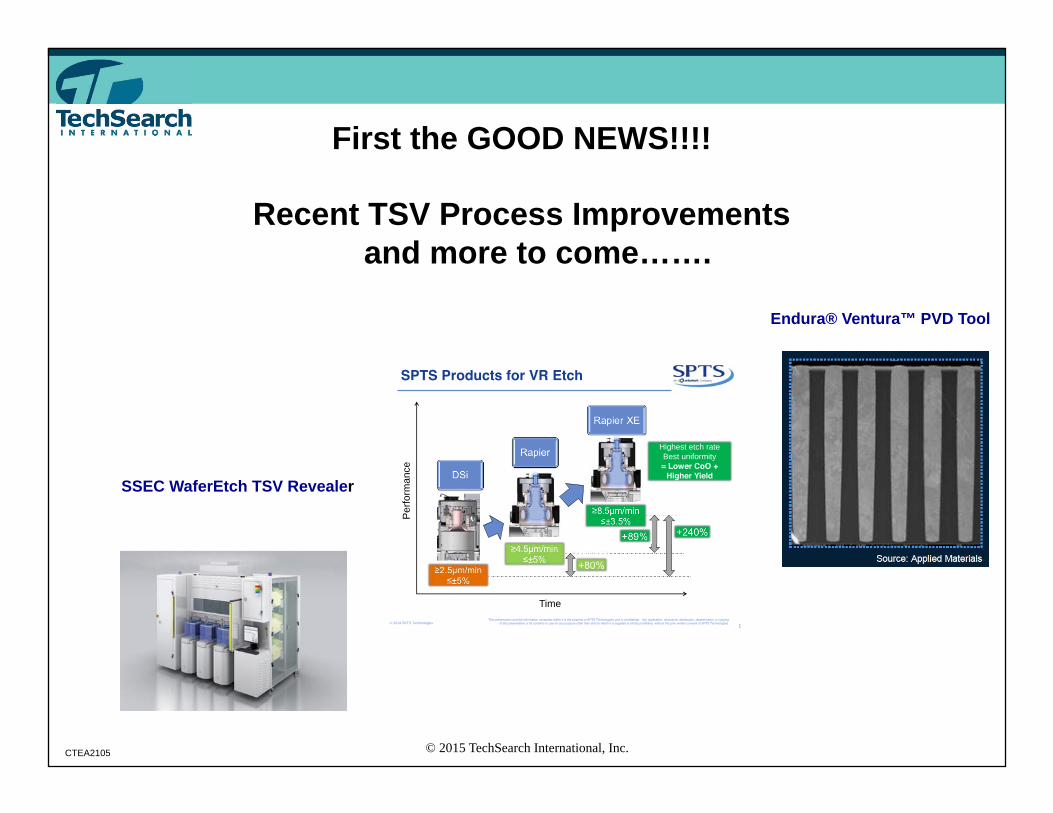
First the GOOD NEWS!!!!
Recent TSV Process Improvements and more to come…….
Endura® Ventura™ PVD Tool
SSEC WaferEtch TSV Revealer
1 This presentation and the information contained within it is the property of SPTS Technologies and is confidential. Any duplication, disclosure, distribution, dissemination or copying
of this presentation or its contents or use for any purpose other than that for which it is supplied is strictly prohibited, without the prior written consent of SPTS Technologies. © 2014 SPTS Technologies
SPTS Products for VR Etch
DSi
Rapier
Rapier XE
±5%
±5%
±3.5% P
erfo
rman
ce
Time
+80%
+89% +240%
Highest etch rate Best uniformity = Lower CoO +
Higher Yield

CTEA2105 © 2015 TechSearch International, Inc.
Now the BAD NEWS: It Takes Time…..
• DRAM stacking R&D at Micron started in 2002, first product in HVM 2015 Samsung delivering RDIMM with stacked die (TSV)
• Xilinx Stacked Silicon Interconnect (Si interposer with TSVs) R&D started in 2006, first HVM in 2012
Source: TechSearch International, Inc.
CTEA2105 © 2015 TechSearch International, Inc.
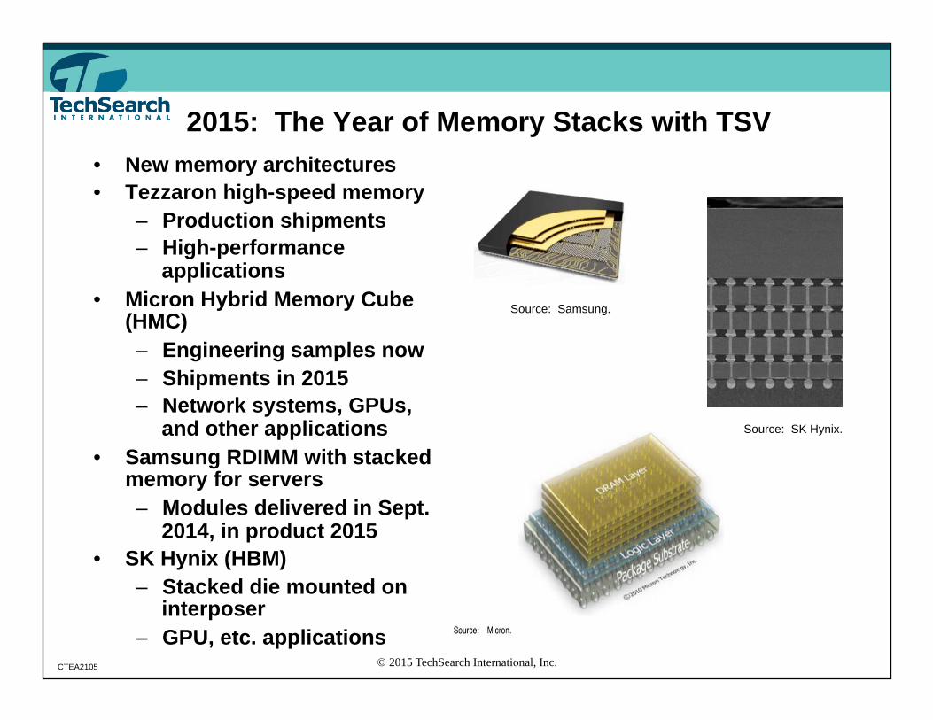
2015: The Year of Memory Stacks with TSV • New memory architectures • Tezzaron high-speed memory
– Production shipments – High-performance
applications • Micron Hybrid Memory Cube
(HMC) – Engineering samples now – Shipments in 2015 – Network systems, GPUs,
and other applications • Samsung RDIMM with stacked
memory for servers – Modules delivered in Sept.
2014, in product 2015 • SK Hynix (HBM)
– Stacked die mounted on interposer
– GPU, etc. applications
Source: Samsung.
Source: SK Hynix.
CTEA2105 © 2015 TechSearch International, Inc.
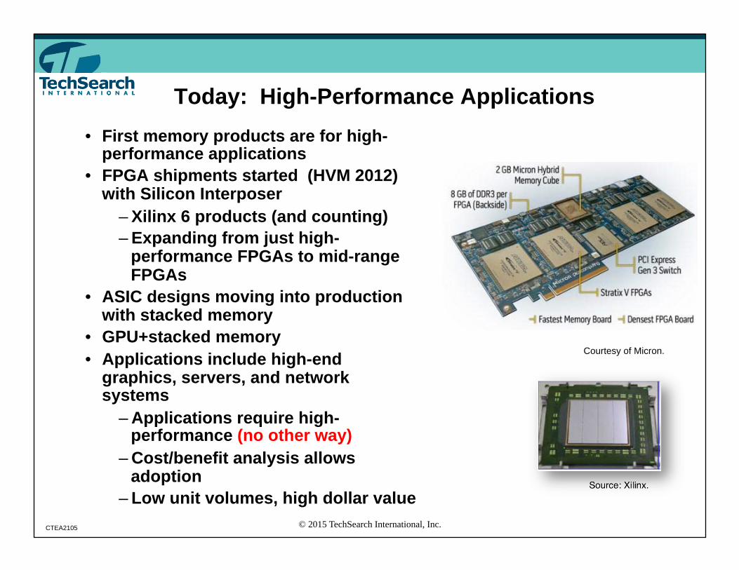
Today: High-Performance Applications • First memory products are for high-
performance applications • FPGA shipments started (HVM 2012)
with Silicon Interposer – Xilinx 6 products (and counting) – Expanding from just high-
performance FPGAs to mid-range FPGAs
• ASIC designs moving into production with stacked memory
• GPU+stacked memory • Applications include high-end
graphics, servers, and network systems
– Applications require high-performance (no other way)
– Cost/benefit analysis allows adoption
– Low unit volumes, high dollar value Source: Xilinx.
Courtesy of Micron.

CTEA2105 © 2015 TechSearch International, Inc.
Challenges for 3D IC Expansion
EDA Tool Availability and Ease of Use
Assembly: Stacking of Die
Wafer Thinning: Debond Process
Thermal: With Logic + Memory Stack
Test Methodology: KGD or KGS
Yield: Impacts Cost
Supply Chain and InfrastructureSource: TechSearch International, Inc.
CTEA2105 © 2015 TechSearch International, Inc.
EDA Tool Challenges • EDA = Automation (difficult to decide what and where to automate
because many different requirements and solutions in development to development to support 3D IC technology) – Floorplanning – Routing – Power/signal integrity – Thermally aware design
• Large memory vendors of HMC and HBM do not need additional tools beyond SPICE simulators – Require redundancy – Require BIST (and repair!) – Require DFT – Products are “new architectures”
• Adoption of 3D IC requires a new system architecture – Design from system level – Co-design required

CTEA2105 © 2015 TechSearch International, Inc.
Process and Architectural Choices: Need Tools • Stack orientation • Technology nodes • Package type • Number of TSVs and location • Keep-out zones (KOZ) • Local/global chip-package interaction,
how to connect die, reliability, and ESD • Timing closure at package level • Power distribution network, signal
integrity, and thermal performance • Requirements or backside re-distribution
layers (BRDLs) • Trade-off for pitch and number of BRDLs • Create blocks to define process, metal/via
topologies, an via profiles

CTEA2105 © 2015 TechSearch International, Inc.
Driving the Narrow Road Between High Cost and Low Reliability
• Function of EDA Tool is to help driving the narrow road between high cost and low reliability

CTEA2105 © 2015 TechSearch International, Inc.
Issues with Temporary Bond/Debond
• Challenge is wafer thinning at ≤50 µm (100µm interposers OK)
• Voids created during the adhesive application process
• Wafer breakage or chipping • Bump deformation during debond • Particles created during process • Damage to wafer from laser or high
temperature processing • Reactions to chemical solvents • Room temperature debonding
required • Almost a dozen companies (and
counting) with bond/debond materials or developments – Requires up to 18 months to
qualify a new process
Adhesive stronger than silicon

CTEA2105 © 2015 TechSearch International, Inc.
Assembly Challenges for 3D ICs • Micro bump
– Pitch typically 40 µm – Cu pillar with solder cap (SnAg, SnCu,
pure Sn, or other alloys) – Other bump metallurgies?
• Assembly – Micro bumps variation may present
bonding challenges – Requires high accuracy bonder (±2µm),
but trade-off is slower speed – T/C bonders >$1 million – Throughput improvements needed, some
new players have entered – Yield must be high
• Underfill material and methods require improvement (No voids allowed) – Probably not capillary flow – Non-conductive paste (NCP)? – Non-conductive film (NCF) some
applications
Source: Samsung.
Source: SK Hynix.

CTEA2105 © 2015 TechSearch International, Inc.
Test Issues for 3D IC with TSV
• Want to minimize total cost of test and test-escape
• Today: “Stack and Pray” = accumulated yield loss
• Today 3D IC memory stacks tested in packages • 100% Test before assembly and after each assembly event
= high test cost
• Do we test through the TSV/micro bump interface or around it?
– Testing a 10,000 micro bump array is difficult and potentially very expensive
– Need to test connections – Need BIST, redundancy, self-repair
1 chip 2 chips 3 chips 4 chips 90% 81% 73% 64%
Source: Adapted from P. Franzon

CTEA2105 © 2015 TechSearch International, Inc.
Why the Delay in Memory + Logic? • Logic and memory stack for
mobile 2018 (at earliest) • Today more expensive than PoP
solution – 3D IC process yield is low – Process steps such as debond
during thinning – Test strategy required – Impacts total cost
• Couples memory and logic supply so can’t easily swap one memory supplier for another
• Business risk (versus alternatives) – Mobile products must meet steep
product ramp • Thermal issues, unless low-power
design is available (requires new architecture)
Source: SK Hynix.

CTEA2105 © 2015 TechSearch International, Inc.
PoP Remains Alternative for AP • Thinner package and smaller
footprint – Today 1.0mm height
requirement – Future ≤0.8 mm
• 3D IC with TSV provides the ultimate in package height reduction, highest density and performance
• PoP in high-end smartphones – Option 1: Continue with FC
on thin substrate – Option 2: Embedded active
die (application processor) in bottom laminate substrate
– Option 3: Fan-out WLP with application processor as bottom package
– Option 4: 3D IC with TSVs for memory and logic stack (requires new architecture to handle thermal constraints, lower cost, and less risk)
Source: Intel
Source: Renesas.
Source: Amkor Technology.

CTEA2105 © 2015 TechSearch International, Inc.
3D IC Design: Thermal is Critical • Low-cost thermal management solutions must be solved in order for 3D IC for logic and
memory to see widespread adoption • Current PoP solution provides better thermal solution • Thermal issues: 3D circuits increase total power generated per unit surface area
– Chips in the stack may overheat of cooling is not provided – Space may be too small for cooling channels (very small gap for fluid flow) – Thinning chips creates extreme conditions for on-chip hot spot – Need new low-power designs
Source: Renesas.

CTEA2105 © 2015 TechSearch International, Inc.
3D IC for Mobile Products?
• Smartphone ASPs continue to decline • Creates price pressure that makes adoption of advanced packaging technology challenging,
especially interposers – Requires low-cost solution AND infrastructure to meet steep ramp
Source: Adapted from IDC.
Source: TechSearch International, Inc.
Source: TPSS.
CTEA2105 © 2015 TechSearch International, Inc.
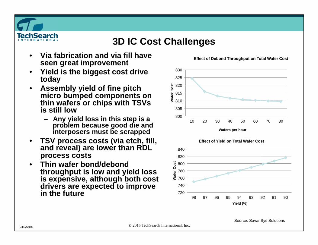
3D IC Cost Challenges • Via fabrication and via fill have
seen great improvement • Yield is the biggest cost drive
today • Assembly yield of fine pitch
micro bumped components on thin wafers or chips with TSVs is still low – Any yield loss in this step is a
problem because good die and interposers must be scrapped
• TSV process costs (via etch, fill, and reveal) are lower than RDL process costs
• Thin wafer bond/debond throughput is low and yield loss is expensive, although both cost drivers are expected to improve in the future
Source: SavanSys Solutions
800
805
810
815
820
825
830
10 20 30 40 50 60 70 80
Waf
er C
ost
Wafers per hour
Effect of Debond Throughput on Total Wafer Cost
720
740
760
780
800
820
840
98 97 96 95 94 93 92 91 90
Waf
er C
ost
Yield (%)
Effect of Yield on Total Wafer Cost

CTEA2105 © 2015 TechSearch International, Inc.
3D IC with TSV Adoption Timeline
• Image sensors with backside vias from Toshiba in January 2008 • Tezzaron DRAM 2013, Micron HMC 2015, SK Hynix HBM 2015, Samsung RDIMM 2015 • Application processor/memory 2018 at earliest • Logic on logic 2019 at earliest • Automotive sensors 2019
Source: TechSearch International, Inc.

CTEA2105 © 2015 TechSearch International, Inc.
Where Does An Interposer Fit?
• Large die fabricated on advanced technology nodes (such as FPGA or large ASIC) – Decrease die size – Increase yield
• Functional optimization – Lower cost to fab
functions on the least expensive technology node
– Allows reuse of design • Logic and memory for power
and performance – Increased Bandwidth – Improved Performance
per Watt
Source: Altera.

CTEA2105 © 2015 TechSearch International, Inc.
Si Interposer Era: The Beginning
• FPGA shipments started (HVM 2012) – Xilinx has at least 6 products – Expanding from just high-performance
FPGAs to mid-range FPGAs • ASIC designs moving into production • GPU+stacked memory • Applications include network systems and
future servers – Applications require high performance – Cost/benefit analysis allows adoption – Low unit volumes, high dollar value
• Potential processor partitioning for mobile products???
– High unit volumes – Needs low-cost solution (not currently
available)
Source: Xilinx.

CTEA2105 © 2015 TechSearch International, Inc.
Conclusions
• 3D IC Status – Applications in production: image sensor + logic – Applications moving into production: stacked memory – Industry is working to resolve issues that will allow 3D IC with TSV
in additional applications – Good engineering work still required to improve yield and lower
cost – Don’t give up!
• 2.5D Interposer Before 3D IC (silicon interposers?, organic? glass?) – ASIC – GPU/CPU – Availability of stacked memory critical for some applications
• Other alternatives (Laminate MCM, Intel’s Silicon Bridge, Xilinx SLIT) • Concern about suppliers and assembly capability are being addressed
– Business models settling down • Cost remains a concern in every discussion
– Yield improvements for process – New architectures are required