the impact of via and pad design on qfn assembly
TRANSCRIPT

THE IMPACT OF VIA AND PAD DESIGN ON QFN ASSEMBLY
Jennifer Nguyen, David Geiger and Anwar Mohammed Flex
Milpitas, CA, USA [email protected]
ABSTRACT Quad Flat No-Lead (QFN) packages has become very popular in the industry and are widely used in many products. These packages have different size and pin counts, but they have a common feature: thermal pad at the bottom of device. The thermal pad of the leadless QFN provides efficient heat dissipation from the component to PCB. In many cases, arrays of the thermal via under the component is used to dissipate heat from the device. However, thermal vias can create more voids or result in solder protrusion onto the secondary side.
This paper discusses our study on the impact of the via size and the via design on QFN voiding and solder protrusion. Do small vias prevent the solder from flowing onto the other side? How should via be designed? Which via type will have less voiding issue? A comprehensive experiment was designed in trying to answer these questions. Different QFN types, via design, via sizes, via pitches and stencil design were studied using three different board thicknesses: 1.6mm, 2.4mm and 3.2 mil thick.
Key words: quad flat no lead (QFN), dual row QFN, single row QFN, thermal pad, voids, voiding, via design, solder protrusion
INTRODUCTION Quad Flat No-Lead (QFN) package is designed in such a way that the thermal pad is exposed on the bottom of the component. This creates a low thermal resistance path between the die and the exterior of the package and provides excellent heat dissipation from the component to the PCB. Thermal vias in the PCB thermal pad are typically used to conduct the heat away from the device and to transfer effectively the heat from the top copper layer of the PCB to the inner or bottom copper layer or to the outside environment. A cross sectional view of QFN and PCB thermal vias is shown in Figure 1.
Figure 1. Cross Section View of QFN and PCB Structure.
There are several publications about the PCB layout guidelines for QFN packages required thermal vias [1-2]. Some recommend thermal vias in the solder mask defined thermal pad [2] while other place the thermal vias directly on the thermal pad without any solder mask [1]. The solder mask around the via can keep the solder away from the via and prevent it from flowing into the via. However, the solder mask ring tends to create more voids or unsoldered areas at the thermal pad. On the other hand, the solder can flow into the thermal vias if there is no solder mask ring and result in solder loss and solder protrusion onto the secondary side, which can interfere with the assembly process and become a quality issue. In this paper, we will discuss the impact of via design, board design and process parameters on solder protrusion at the thermal pad’s vias. QFN voiding is a known industry challenge with many publications [3,4,5,6]. The influence of via design and processes on voiding will also be presented in the paper.
EXPERIMENTAL DETAILS Test Vehicle and Components A QFN test vehicle was designed for this study. The test vehicle had the dimension of 177x177mm. The board surface finish was immersion silver (I-Ag). Three different board thicknesses of 1.6mm (62mil), 2.4mm (93mil) and 3.2mm (125mil) were investigated. The image of the test vehicle is shown in Figure 2.
Thermal Pad QFN Component
Solder
Thermal Via
PCB
Proceedings of SMTA International, Sep. 25 - 29, 2016, Rosemont, IL, USA Page 143
As originally published in the SMTA Proceedings
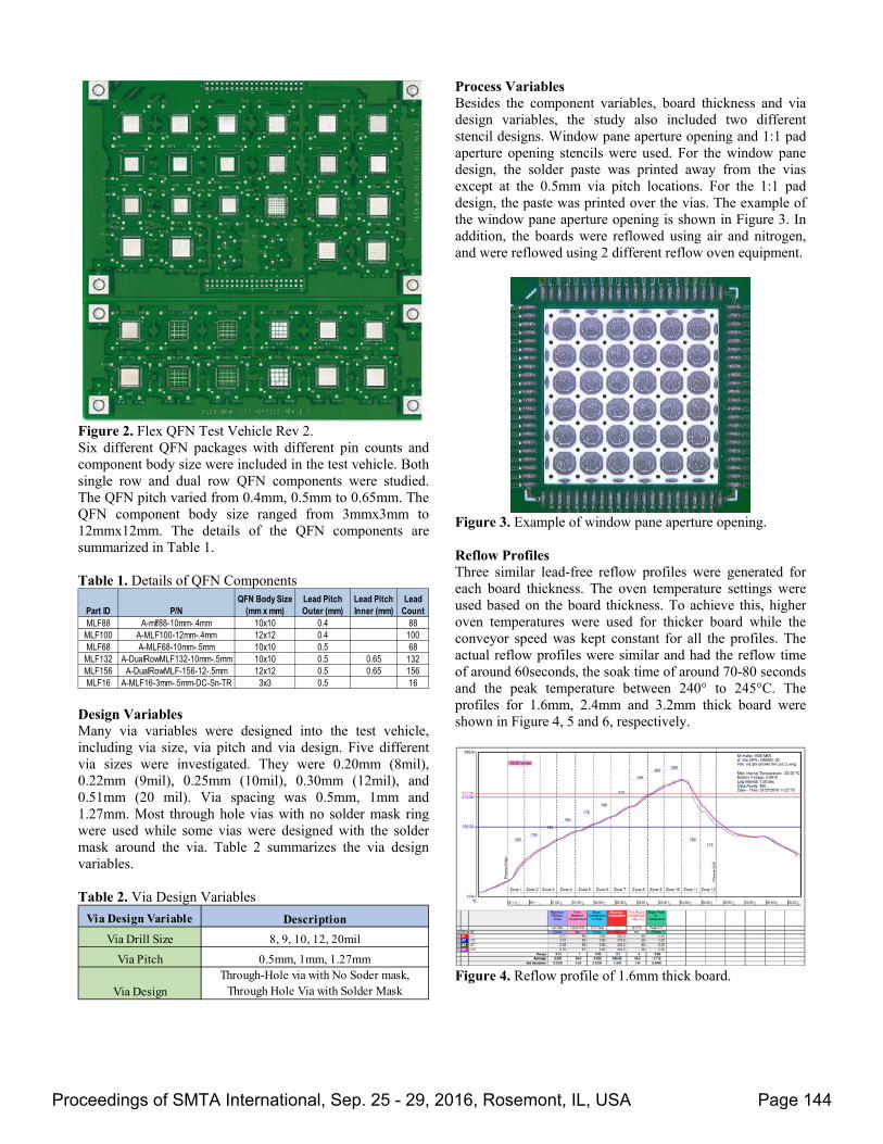
Figure 2. Flex QFN Test Vehicle Rev 2. Six different QFN packages with different pin counts and component body size were included in the test vehicle. Both single row and dual row QFN components were studied. The QFN pitch varied from 0.4mm, 0.5mm to 0.65mm. The QFN component body size ranged from 3mmx3mm to 12mmx12mm. The details of the QFN components are summarized in Table 1. Table 1. Details of QFN Components
Design Variables Many via variables were designed into the test vehicle, including via size, via pitch and via design. Five different via sizes were investigated. They were 0.20mm (8mil), 0.22mm (9mil), 0.25mm (10mil), 0.30mm (12mil), and 0.51mm (20 mil). Via spacing was 0.5mm, 1mm and 1.27mm. Most through hole vias with no solder mask ring were used while some vias were designed with the solder mask around the via. Table 2 summarizes the via design variables. Table 2. Via Design Variables
Process Variables Besides the component variables, board thickness and via design variables, the study also included two different stencil designs. Window pane aperture opening and 1:1 pad aperture opening stencils were used. For the window pane design, the solder paste was printed away from the vias except at the 0.5mm via pitch locations. For the 1:1 pad design, the paste was printed over the vias. The example of the window pane aperture opening is shown in Figure 3. In addition, the boards were reflowed using air and nitrogen, and were reflowed using 2 different reflow oven equipment.
Figure 3. Example of window pane aperture opening. Reflow Profiles Three similar lead-free reflow profiles were generated for each board thickness. The oven temperature settings were used based on the board thickness. To achieve this, higher oven temperatures were used for thicker board while the conveyor speed was kept constant for all the profiles. The actual reflow profiles were similar and had the reflow time of around 60seconds, the soak time of around 70-80 seconds and the peak temperature between 240° to 245°C. The profiles for 1.6mm, 2.4mm and 3.2mm thick board were shown in Figure 4, 5 and 6, respectively.
Figure 4. Reflow profile of 1.6mm thick board.
Part ID P/NQFN Body Size
(mm x mm)Lead Pitch Outer (mm)
Lead Pitch Inner (mm)
Lead Count
MLF88 A-mlf88-10mm-.4mm 10x10 0.4 88MLF100 A-MLF100-12mm-.4mm 12x12 0.4 100MLF68 A-MLF68-10mm-.5mm 10x10 0.5 68
MLF132 A-DualRowMLF132-10mm-.5mm 10x10 0.5 0.65 132MLF156 A-DualRowMLF-156-12-.5mm 12x12 0.5 0.65 156MLF16 A-MLF16-3mm-.5mm-DC-Sn-TR 3x3 0.5 16
Via Design Variable Description
Via Drill Size 8, 9, 10, 12, 20mil
Via Pitch 0.5mm, 1mm, 1.27mm
Via DesignThrough-Hole via with No Soder mask,
Through Hole Via with Solder Mask
Proceedings of SMTA International, Sep. 25 - 29, 2016, Rosemont, IL, USA Page 144

Figure 5. Reflow profile of 2.4mm thick board.
Figure 6. Reflow profile of 3.2mm thick board. RESULTS AND DISCUSSION Via Measurement The via diameter of different via sizes were measured before the assembly. Both drill size and hole size were measured as shown in Figure 7.
Figure 7. Drill Size and Hole Size Definition The measured drill sizes were consistent and close to the theoretical drill sizes. The hole size was smaller than the drill size. It was expected because of the copper plating at the via. The drill size measurements of different board thicknesses are shown in Table 3-5, and the actual hole size measurements are shown in Table 6-8, respectively.
Table 3. Drill Size Measurement for 1.6mm Thick Board
Table 4. Drill Size Measurement for 2.4 mm Thick Board
Table 5. Drill Size Measurement for 3.2 mm Thick Board
Table 6. Actual Hole Size Measurement for 1.6mm Thick Board.
Drill Size Measurement_
62mil Thick PCB U1 U2 U3 U4 U43
Theoretical Drill Size [10mil] [9mil] [8mil] [12mil] [20mil]
1 9.9 8.91 7.4 11.97 19.13
2 9.98 8.95 7.48 11.89 19.21
3 10.06 8.71 7.68 11.65
4 9.82 8.47 7.52 11.73
5 9.9 9.03 7.75 11.53
6 9.82 8.87 7.12 11.69
7 9.86 8.99 7.68 11.77
Average 9.91 8.85 7.52 11.75 19.17
STDEV 0.09 0.20 0.22 0.15 0.06
Drill Size Measurement_
93mil Thick PCB U1 U2 U3 U4 U43
Theoretical Drill Size [10mil] [9mil] [8mil] [12mil] [20mil]
1 10.1 8.83 7.99 11.81 18.73
2 9.9 8.91 7.87 11.85 18.53
3 10.02 8.91 7.95 11.25
4 9.9 8.75 7.83 11.49
5 9.94 8.91 7.87 11.45
6 9.94 9.19 7.6 11.49
7 9.94 9.11 7.95 12.01
Average 9.96 8.94 7.87 11.62 18.63
STDEV 0.07 0.15 0.13 0.27 0.14
Drill Size Measurement_
125mil Thick PCB U1 U2 U3 U4 U43
Theoretical Drill Size [10mil] [9mil] [8mil] [12mil] [20mil]
1 10 9.24 8.03 12.17 19.81
2 10.12 9.08 7.99 12.13 19.44
3 10 9.08 8.24 12.21
4 10.04 9.16 8.07 12.05
5 9.88 9 8.28 11.93
6 9.88 8.92 8.16 11.89
7 9.96 8.88 8.24 11.89
Average 9.98 9.05 8.14 12.04 19.63
STDEV 0.09 0.13 0.12 0.14 0.26
Actual Hole Size
Measurement_ 1.6mm
Thick PCB U1 U2 U3 U4 U43
Theoretical Drill Size [10mil] [9mil] [8mil] [12mil] [20mil]
1 7.79 6.76 5.21 9.58 16.5
2 7.68 6.8 5.29 9.58 16.8
3 7.79 6.56 5.69 9.27
4 7.64 6.2 5.33 9.35
5 7.72 7 5.65 9.27
6 7.56 6.72 4.85 9.31
7 7.4 6.88 5.53 9.5
Average 7.65 6.70 5.36 9.41 16.65
STDEV 0.14 0.26 0.29 0.14 0.21
Hole Size
Drill Size
Proceedings of SMTA International, Sep. 25 - 29, 2016, Rosemont, IL, USA Page 145
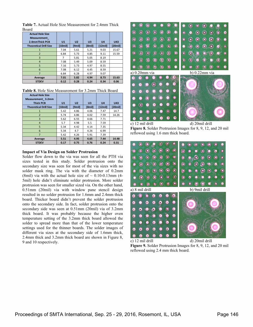
Table 7. Actual Hole Size Measurement for 2.4mm Thick Board
Table 8. Hole Size Measurement for 3.2mm Thick Board
Impact of Via Design on Solder Protrusion Solder flow down to the via was seen for all the PTH via sizes tested in this study. Solder protrusion onto the secondary size was seen for most of the via sizes with no solder mask ring. The via with the diameter of 0.2mm (8mil) via with the actual hole size of ~ 0.10-0.13mm (4-5mil) hole didn’t eliminate solder protrusion. More solder protrusion was seen for smaller sized via. On the other hand, 0.51mm (20mil) via with window pane stencil design resulted in no solder protrusion for 1.6mm and 2.4mm thick board. Thicker board didn’t prevent the solder protrusion onto the secondary side. In fact, solder protrusion onto the secondary side was seen at 0.51mm (20mil) via of 3.2mm thick board. It was probably because the higher oven temperature setting of the 3.2mm thick board allowed the solder to spread more than that of the lower temperature settings used for the thinner boards. The solder images of different via sizes at the secondary side of 1.6mm thick, 2.4mm thick and 3.2mm thick board are shown in Figure 8, 9 and 10 respectively.
a) 0.20mm via b) 0.22mm via
c) 12 mil drill d) 20mil drill Figure 8. Solder Protrusion Images for 8, 9, 12, and 20 mil reflowed using 1.6 mm thick board.
a) 8 mil drill b) 9mil drill
c) 12 mil drill d) 20mil drill Figure 9. Solder Protrusion Images for 8, 9, 12, and 20 mil reflowed using 2.4 mm thick board.
Actual Hole Size
Measurement_
2.4mmThick PCB U1 U2 U3 U4 U43
Theoretical Drill Size [10mil] [9mil] [8mil] [12mil] [20mil]
1 7.04 5.61 5.21 9.03 15.67
2 6.84 5.73 4.85 9.11 15.59
3 7 5.81 5.05 8.19
4 7.08 5.49 5.09 8.59
5 7.16 5.73 4.97 8.55
6 7.08 6.12 4.45 8.59
7 6.84 6.28 4.97 9.07
Average 7.01 5.82 4.94 8.73 15.63
STDEV 0.12 0.28 0.24 0.34 0.06
Actual Hole Size
Measurement_ 3.2mm
Thick PCB U1 U2 U3 U4 U43
Theoretical Drill Size [10mil] [9mil] [8mil] [12mil] [20mil]
1 5.42 4.86 4.06 7.47 14.7
2 5.74 4.86 4.02 7.59 14.26
3 5.62 6.55 4.66 7.71
4 5.7 4.98 5.5 7.59
5 5.34 4.42 4.14 7.35
6 5.34 4.7 4.26 6.99
7 5.42 4.26 5.91 7.39
Average 5.51 4.95 4.65 7.44 14.48
STDEV 0.17 0.75 0.76 0.24 0.31
Proceedings of SMTA International, Sep. 25 - 29, 2016, Rosemont, IL, USA Page 146

a) 8 mil drill b) 9mil drill
c) 0.30mm via d) 0.51mm via Figure 10. Solder Protrusion Images for 8, 9, 12, and 20 mil reflowed using 3.2mm thick board. The solder mask ring helped to prevent the solder from getting into the via. No solder protrusion was seen for the via 12 mil in dimension, designed with the solder mask ring using window pane stencil design, as shown in Figure 11.
a) No SM Ring b) With Solder mask
Figure 11. Visual Images of solder at the secondary side for through hole via with no solder mask and for through hole via with solder mask ring around the via. Impact of Via and Pad Design on Voiding On the contrary, the through hole via with solder mask ring showed more voiding area as compared to the through hole
via with no solder mask ring (Figure 12). Voiding difference due to different via size was insignificant (Figure 13).
a) PTH via with no SM b) PTH via with SM
Figure 12. X-ray images of QFN with no solder mask ring around thermal via and with the solder mask ring around the thermal via. a) PTH via with no solder mask, b) PTH via with solder mask ring.
a) 0.20mm via b) 0.22mm via
c) 0.25mm via d) 0.3mm via Figure 13. Impact of via size on voiding. The study showed that PTH via resulted in less voids and smaller voids than no via and via in pad. It was because PTH via created a channel for air outgassing during the reflow and solder joint formation. The voiding x-ray images of the thermal pad designed with no via and via in pad are shown in Figure 14.
Proceedings of SMTA International, Sep. 25 - 29, 2016, Rosemont, IL, USA Page 147
a) No via b) Via in Pad
Figure 14. Voiding images of QFN thermal pad with no via, and with via in pad. Breaking the large thermal pad into smaller pads resulted in smaller voids. However, the overall void percentage didn’t decrease significantly (Figure 15).
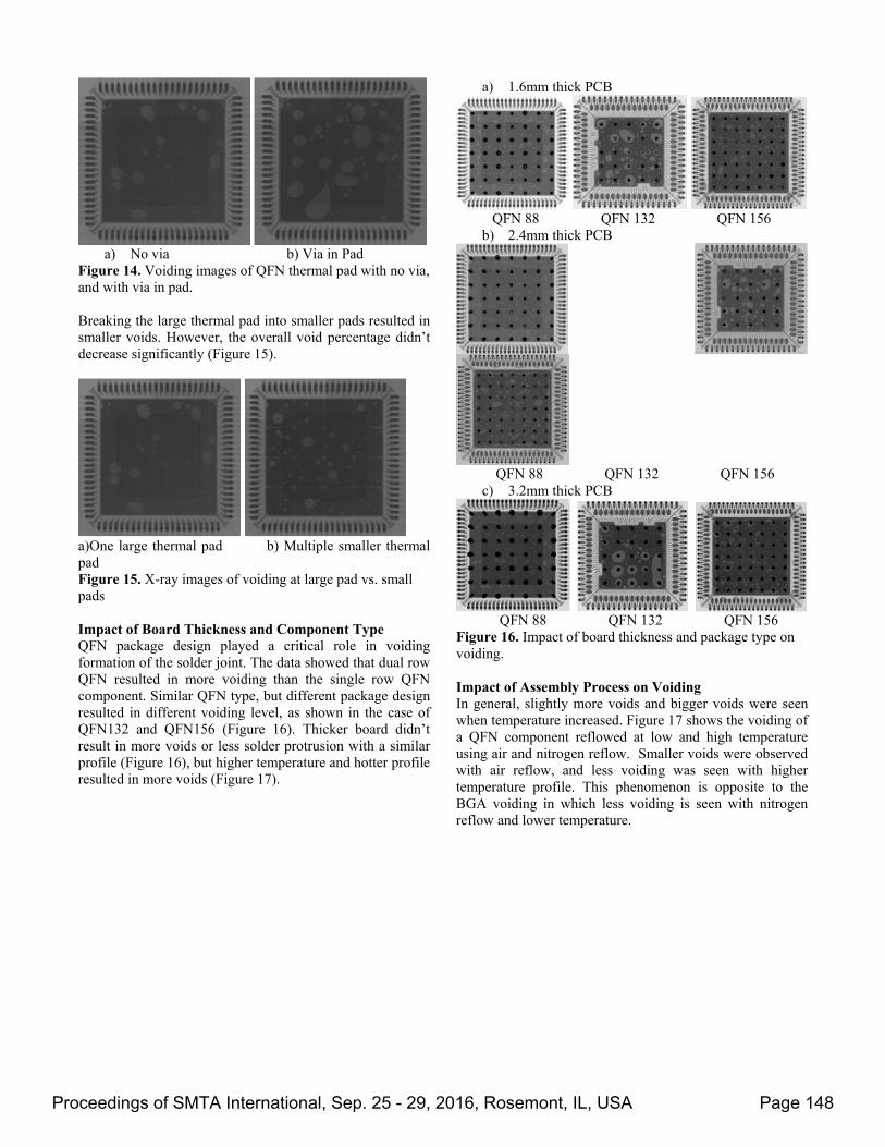
a)One large thermal pad b) Multiple smaller thermal pad Figure 15. X-ray images of voiding at large pad vs. small pads Impact of Board Thickness and Component Type QFN package design played a critical role in voiding formation of the solder joint. The data showed that dual row QFN resulted in more voiding than the single row QFN component. Similar QFN type, but different package design resulted in different voiding level, as shown in the case of QFN132 and QFN156 (Figure 16). Thicker board didn’t result in more voids or less solder protrusion with a similar profile (Figure 16), but higher temperature and hotter profile resulted in more voids (Figure 17).
a) 1.6mm thick PCB
QFN 88 QFN 132 QFN 156
b) 2.4mm thick PCB
QFN 88 QFN 132 QFN 156
c) 3.2mm thick PCB
QFN 88 QFN 132 QFN 156 Figure 16. Impact of board thickness and package type on voiding. Impact of Assembly Process on Voiding In general, slightly more voids and bigger voids were seen when temperature increased. Figure 17 shows the voiding of a QFN component reflowed at low and high temperature using air and nitrogen reflow. Smaller voids were observed with air reflow, and less voiding was seen with higher temperature profile. This phenomenon is opposite to the BGA voiding in which less voiding is seen with nitrogen reflow and lower temperature.
Proceedings of SMTA International, Sep. 25 - 29, 2016, Rosemont, IL, USA Page 148
a) Low profile/ Air b) High profile/Air
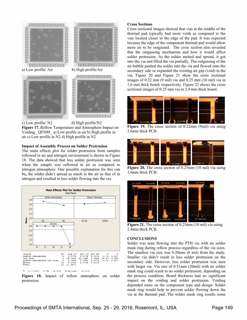
c) Low profile/ N2 d) High profile/N2 Figure 17. Reflow Temperature and Atmosphere Impact on Voiding_ QFN88_ a) Low profile in air b) High profile in air c) Low profile in N2 d) High profile in N2 Impact of Assembly Process on Solder Protrusion The main effects plot for solder protrusion from samples reflowed in air and nitrogen environment is shown in Figure 18. The data showed that less solder protrusion was seen when the sample was reflowed in air as compared to nitrogen atmosphere. One possible explanation for this can be, the solder didn’t spread as much in the air as that of in nitrogen and resulted in less solder flowing into the via.
Figure 18. Impact of reflow atmosphere on solder protrusion.
Cross Sections Cross sectional images showed that vias at the middle of the thermal pad typically had more voids as compared to the vias located closer to the edge of the pad. It was expected because the edge of the component thermal pad would allow more air to be outgassed. The cross section also revealed that the outgassing mechanism and how it would affect solder protrusion. As the solder melted and spread, it got into the via and filled the via partially. The outgassing of the air bubble pushed the solder into the via and flowed onto the secondary side or expanded the existing air gap (void) in the via. Figure 20 and Figure 21 show the cross sectional images of 0.22 mm (9 mil) via and 0.25 mm (10 mil) via in 1.6 mm thick board, respectively. Figure 22 shows the cross sectional images of 0.25 mm via in 2.4 mm thick board.
Figure 19. The cross section of 0.22mm (9mil) via using 1.6mm thick PCB.
Figure 20. The cross section of 0.25mm (10 mil) via using 1.6mm thick PCB.
Figure 21. The cross section of 0.25mm (10 mil) via using 2.4mm thick PCB. CONCLUSIONS Solder was seen flowing into the PTH via with no solder mask ring during reflow process regardless of the via sizes. The smallest via size was 0.20mm (8 mil) from the study. Smaller via didn’t result in less solder protrusion on the secondary side. However, less solder protrusion was seen with larger via. Via size of 0.51mm (20mil) with no solder mask ring could result in no solder protrusion, depending on the process condition. Board thickness had no significant impact on the voiding and solder protrusion. Voiding depended more on the component type and design. Solder mask ring would help to prevent solder flowing down the via at the thermal pad. The solder mask ring results some
AirN2
3.0
2.5
2.0
1.5
1.0125mil62 mil
20121098
3.0
2.5
2.0
1.5
1.0
Reflow Atmosphere
Mea
n
Board Thickness
Via Size
Main Effects Plot for Solder ProtrusionData Means
Proceedings of SMTA International, Sep. 25 - 29, 2016, Rosemont, IL, USA Page 149

unsoldered area under the QFN component, which looks like more voiding at the QFN thermal pad. ACKNOWLEDGEMENTS The authors would like to thank Dennis Willie and Robert Pennings at Flex AEG Labs in Milpitas for their help in the assembly. Many thanks to Tu Tran and Francoise Sarrazin at Flex AEG Milpitas lab for the cross section images. REFERENCES [1] Quan Li, Lu Li, Richard Rowan, and Mahesh Shah, “PCB Layout Guidelines for PQFN/QFN Style Packages Requiring Thermal Vias for Heat Dissipation”, Freescale Application Note 3378. [2] Yang Boon Quek, “QFN Layout Guidelines,” Texas Instruments Application Report, SLOA122- July 2006 [3]Jennifer Nguyen, David Geiger and Dongkai Shangguan, Ph. D, “Assembly Challenges of Bottom Terminated Components,” Proceeding of APEX2012, San Diego, CA, 2012. [4] Jennifer Nguyen, David Geiger and Murad Kurwa “Voiding Mitigation of Bottom Terminated Components,” Proceeding of SMTAI’13, 2013. [5] Derrick Herron, Dr. Yan Liu, and Dr. Ning-Cheng Lee, “Voiding Control for QFN Assembly, ” SMTA Pan Pacific, 2011. [6] Richard Coyle, Heather McCormick, Peter Read, Richard Popowich, and Debra Fleming, “ Temperature Cycling Performance of a Quad Flat No Lead (QFN) Package Assembled with Multiple Pb-Free Solders” Proceedings of SMTAi conference, 2003
Proceedings of SMTA International, Sep. 25 - 29, 2016, Rosemont, IL, USA Page 150