the impact of space radiation requirements and effects … · the impact of space radiation...
TRANSCRIPT
THE IMPACT OF SPACE RADIATION REQUIREMENTS
AND EFFECTS ON ASIMS
C. Barnes, A. Johnston and G. SwiftJet Propulsion Laboratory
California Institute of TechnologyPasadena, CA 91109"
f
_S
ABSTRACT
The evolution of highly miniaturized electronic and mechanical systems will be accompanied bynew problems and issues regarding the radiation response of these systems in the space environment. Inthis paper we will discuss some of the more prominent radiation problems brought about by miniaturiza-tion. For example, autonomous microspacecraft will require large amounts of high density memory, mostlikely in the form of stacked, multichip modules of DRAMs, that must tolerate the radiation environment.However, advanced DRAMs (16 to 256 Mbit) are quite susceptible to radiation, particularly single eventeffects, and even exhibit new radiation effects phenomena that were not a problem for older, less densememory chips. Another important trend in microspacecraft electronics is toward the use of low voltagemicroelectronic systems that consume less power. However, the reduction in operating voltage also carrieswith it an increased susceptibility to radiation. In the case of application specific integrated circuits (ASICs)that are an integral part of application specific integrated microinstruments (ASIMs), advanced devices ofthis type, such as high density field programmable gate arrays (FPGAs) exhibit new single event effects(SEE), such as single particle reprogramming of anti-fuse links. New advanced linear bipolar circuits havebeen shown recently to degrade more rapidly in the low dose rate space environment than in the typicallaboratory total dose radiation test used to qualify such devices. Thus, total dose testing of these parts is nolonger an appropriately conservative measure to be used for hardness assurance. We also note that thefunctionality of micromechanical Si-based devices may be altered due to the radiation-induced depositionof charge in the oxide passivation layers.
INTRODUCTION
Risk mitigation through the application of quality assurance techniques to microelectromechamcalsystems (MEMS) will pose special problems for future spacecraft and satellites. The rapid evolution ofnew technologies that are attractive for space applications, the increased emphasis on use of commercialmicroelectronic parts to save cost and schedule, the very small market represented by both military andcivilian space systems, and the emergence of new device failure phenomena all pose particular difficultiesfor insuring flight mission success. Nowhere is this more apparent than in the case of radiation effects, andthe effort to establish radiation hardness assurance (RHA) for MEMS. In the case of other reliability phe-
nomena, one can take advantage of other high volume, high reliability applications, such as automotiveand medical, to leverage statistical measures of reliability, minimum cost and quick schedule, but radiationrepresents a unique requirement not encountered by other high volume application areas. In addition, thedownturn in DoD hardened electronic part development, testing and acquisition has resulted in reducedavailability of radiation hardened or even radiation tolerant electronic parts. With regard to the fabrication
of microelectromechanical parts, most reliability phenomena can be detected or prevented by prudent useof statistical process control and various screening techniques. In the case of radiation effects, however,very often "improvements" in device performance characteristics achieved by altered processing steps canlead to increased radiation vulnerability which only becomes known after the fact during radiation testing.Lastly, many new, emerging technologies exhibit new and unexpected radiation effects that must be takeninto account prior to insertion in space systems. In this paper, we briefly explore some of the radiationeffects issues that will confront designers and users of advanced, microelectronic and microelectromechanical
parts.
There are several ways this discussion can be organized; we have chosen to discuss radiation ef-fects according to part type, beginning with a review of radiation effects in advanced bipolar devices.
*The work described in this paper was carried out by the Jet Propulsion Laboratory, California Institute of Technology, undercontract with the National Aeronautics and Space Administration (NASA). Work was funded by the NASA Code QW sponsoredMicroelectronics Space Radiation Effects Program (MSREP).
https://ntrs.nasa.gov/search.jsp?R=19960054134 2018-06-14T09:25:29+00:00Z

ENHANCED LOW DOSE RATE EFFECTS IN BIPOLAR CIRCUITS
Relatively simple bipolar circuits such as operational amplifiers and comparators, form an essentialpart of many electronic circuits, hybrids and systems. Such devices will continue to play an integral role inthe functionality of advanced devices such as MEMS. Thus, their radiation response will influence theability of MEMS to survive the hostile space radiation environment.
Recently, it has been established [1-10] that many bipolar integrated circuits are much more sus-ceptible to ionizing radiation at low dose rates (0.001 to 0.005 rad(Si)/sec) than they are at the high doserates typically used for radiation testing of parts in the laboratory. Since the low dose rate regime is equiva-lent to that encountered in space, for these devices the standard laboratory radiation test at moderate to highdose rates is no longer conservative. The seriousness of this problem has led the Air Force to issue an AlertConcern for this effect. Because of the greater radiation sensitivity at very low dose rates, the only way to
provide radiation hardness assurance to designers is to perform a radiation test at low dose rates which byits nature is very time consuming. Consequently, it is imperative that an RHA test be developed which canbe performed at moderate to high dose rates. Because the physical mechanism for the enhanced low doserate effect is not yet completely understood, it is not possible to propose a reliable RHA test. Herein, wewill merely provide some examples of this effect, which serve to emphasize the seriousness of the en-hanced low dose rate susceptibility problem.
Initial work [1] on the enhanced low dose rate (ELDR) effect suggested that as the dose rate wasdecreased, the enhancement effect saturated at around i0 rad(Si)/s and did not become any stronger at
lower dose rates. However, expanded studies [2-10] of the ELDR effect clearly indicate that for manydevices, saturation, if and when it occurs, must come at very low dose rates. For example, Figure 1 shows
how input offset voltage, Vos, of the LM324 operational amplifier depends on total dose at different doserates. Note that while there is little change in Vos for dose rates as low as 0.005 rad(Si)/s, there is a dramaticdecrease in offset voltage at low doses when tl'i-_LM324 is irradiated at 0.002 rad(Si)/s. The change in Vosmay come at even lower doses if one were to expose the part at 0.001 rad(Si)/s. To understand how imprac-tical an RHA test becomes under these conditions, suppose that a mission has a total dose requirement of15 krad(Si) and testing must be done at 0.001 rad(Si)/s to obtain the lowest failure dose because of the typeof behavior shown in Figure 1. In order to test to the mission requirement, the radiation exposure wouldlast for nearly 6 months, a test time that would be prohibitive for many fast, aggressive flight projects.
I I I I I I I
50 rad(Si)/s
0.005 rad(Si)/s
0.002 rad(Si)/s
-15 I
LM 324 Operational Amplifier
Substrate pnp Input TransistorI I I / 1
0 10 20 30 40 50 60 70 80
Total Dose krad(Si)
Figure 1. Degradation of input offset voltage of the LM324 operational amplifier at various dose rates.
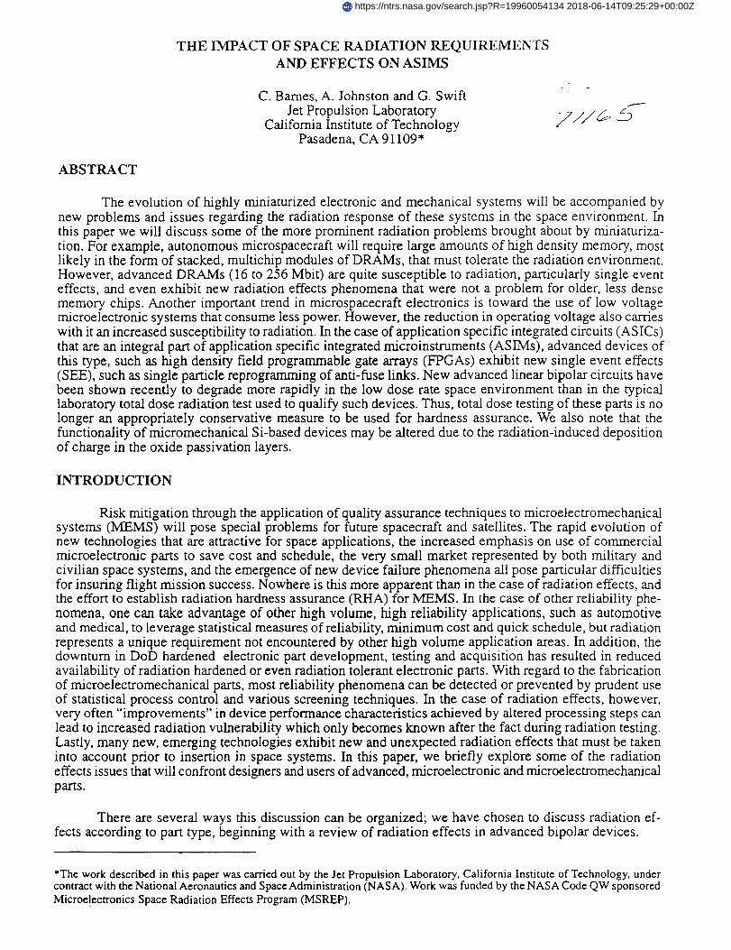
Studies of the response of individual bipolar transistor types to different dose rates have shown thatthe problem is most severe for pnp transistors used in many linear circuits with conventional junction
isolation. Damage in pnp devices can be 6 to 7 times greater at low dose rates than at high dose rates [4]. Incontrast, npn transistors from the same fabrication processes are generally not sensitive to dose rate effectsbelow approximately 1 rad(Si)/s. Thus, circuits which use both types of components may exhibit different
failuremodesatlow andhighdoseratesbecauseof thedifferentamountof relativedamagethatoccursinthe two typesof componenttransistorsat low doserates.In addition,different bipolar circuits that usevaryingmixesof thetwo transistortypescanexhibit differentfailurecharacteristics,evenfor parts fromthesameprocessline. Forexample,Figure2comparesinputbiascurrentdegradationof two bipolarcircuittypeswith similar input stagedesignsfrom thesamemanufacturer.Doserateeffectsarerelatively easytoevaluatein linearcircuits with pnp input transistors because the input bias current provides a straightfor-ward way to measure input transistor gain degradation. For the LM 111 and LM324 shown in Figure 2, bothdevices use substrate pnp transistors, but the typical value of input bias current is three times greater for theLM 111 than for the LM324. Although both circuits are more damaged when they are irradiated at low doserate, degradation in the LM324 is much greater. Damage in the LM111 saturates at relatively low total doselevels, reducing the significance of enhanced damage. Input bias current of the LM324 continues to de-grade at low dose rate as the radiation level increases, and consequently it is well above the specificationlimit even at 10 krad(Si). Even higher damage occurred in this device at 0.002 rad(Si)/s, although this is notshown in Figure 2. These results show that large differences can occur between different circuit typesproduced by the same manufacturer, and that it is risky to make blanket assessments about dose rate effectson the basis of tests on a small number of device types.
450
J400 - ,I"
,lit
g 350- 0.005 rad(Si_s//_._._
200-
;= lso- K ,Mlll
/I //_ _ ......... _ _ p' 5o raO(Si)ls
0 5 10 15 20 25 30 35 40
Total Dose [krad(Si)]
Figure 2. Degradation of input bias current of two different bipolar circuits with similar input stages fromthe same manufacturer.
It has also been shown [4] that the same device type from different manufacturers can exhibitsignificantly different ELDR effects. For example, Figure 3 shows input bias current degradation for LM 111voltage comparators, which use substrate pnp input transistors, procured from three different vendors, andtested at two widely different dose rates. For two of the manufacturers, damage of the input transistors isabout six times greater at low dose rates so that they exhibit rapid increases in input bias current at thelower dose rate of 0.005 rad(Si)/s. Devices from the third manufacturer (vendor A) show only a small
increase in damage at the lowest dose rate, even though the geometry of the input transistors of this vendorare identical to that of the vendor with the highest damage at low dose rates. Thus, determination of theextent of the ELDR effect for a particular device type is not sufficient to provide RHA if a different vendor
is selected than the one used for radiation test samples.

1o00
100
r-
lo
- I 1 t I i
I-
- _ Vendor A ! .....
I I I I I0 5 10 15 20 25 30
Total Dose [krad(Si)]
Figure 3. Total dose degradation of LMlll comparators from three different manufacturers at high and
very low dose rates.
The remaining challenge for the radiation effects community is to devise an RHA test for the ELDReffect other than direct testing at very low dose rates, an expensive and time consuming alternative whichis unacceptable, but necessary in some cases at this time. While the physical mechanism of the ELDReffect has not been completely defined, promising models are being developed [3,6] that are associatedwith the dynamics of radiation-induced electrons and holes in thick oxides with weak electric fields. Oneof the approaches suggested by these models is irradiation at moderate to high dose rates at elevated
temperature. Recent work [3,7] has shown that the increased damage at low dose rates can be at leastpartially reproduced by irradiating at high dose rates and at 60°C to 100*C for certain device types fromparticular vendors. However, it is not clear what the temperature should be for a given process technology,or whether or not saturation of the increase in damage will occur at a reasonable temperature. Until the high
temperature RI--IA test is better defined, another way to deal with this problem is to require tests at twodifferent dose rates, selecting the lower dose rate so that it is sufficiently high to allow tests to be completedin days or weeks instead of the extremely long time periods imposed by the very low dose rates discussedabove. Although this is not a substitute for doing tests at very low dose rates for devices that have severeenhanced damage at low dose rate, it is a more pragmatic way to identify devices that have minimalsensitivity to dose-rate effects. JPL has implemented this approach for several devices, using 0.02 rad(Si)/s for the lowest dose rate.
CATASTROPHIC SINGLE EVENT EFFECTS IN FPGAs
Field programmable gate arrays (FPGAs) are enjoying rapidly expanding us_e in advanced elec-tronic systems because of their performance and versatility. In many cases these devices can replace an
entire board populated with discrete devices, thus leading to weight and power savings in spacecraft sys-tems. In addition, field programmable devices offer a versatility that is important for low volume userssuch as civilian and military spacecraft and satellites. The increased insertion of FPGAs in space systemswill require that their performance in radiation environments be well-established. In this section we de-scribe a new single particle-induced dielectric rupture phenomenon that may become an increasingly im-portant single event effect as scaling reduces the characteristic dimensions of FPGAs and similar devices.Because many types of MEMS include dielectric layers (in capacitors and transistors, for example) withvoltages across them, this rupture mechanism is relevant to radiation hardness of MEMS technologies.

Recent SEE testing and research [1 i-13] on FPGAs has revealed a new catastrophic failure mecha-nism in these devices, termed single event dielectric rupture (SEDR), an effect similar to single event gaterupture (SEGR) in power MOSFETs [14,15]. In the Actel A1280 FPGAs that were studied, roughly halfthe silicon real estate on the chip is devoted to logic modules, while the other half consists of the interc0n-nection matrix. As shown in Figure 4, the matrix consists of horizontal and vertical conductors with an
anti-fuse at each crossing point. The anti-fuse structure, shown in Figure 5, consists of a thin (approxi-mately 120 _) sandwich of oxide-nitride-oxide (ONO). The conductors are connected at crossing points(anti-fuses) by electrically inducing dielectric breakdown of the ONO to establish a low resistance connec-tion. A typical programmed FPGA design will have a few percent of the possible total number of anti-fuses(about 650,000 for the A1280) connected to establish the intended functionality of the chip. A randomunconnected anti-fuse will be biased when the logic levels on the two crossing conductors are different, theoccurrence of which depends on the duty cycle and phase of the two signals on these lines. When the bias
is present, say at a level of 5.5 V, the electric field across the thin ONO anti-fuse is approximately 6 MV/cm. As in the case of a power MOSFET gate oxide, this field is large enough to result in rupture of the
oxide due to the passage of a heavy, energetic charged particle. The effect of the resulting partial connec-tion of the conductors depends on the surrounding circuitry and can be either benign or can compromisethe functionality of the FPGA circuit.
VERTICAL CONTROL '11 "11dl .11
VERTICAL TRACK SEGMENT .__q,
CROSS ANTIFUSE -_ " '" ""
,,,),; ,,;
VERTICAL PASS TRANSISTOR __ 1) ( ) ()
il I 1 I
I
LOGIC MODULE > ,, ,t
4 GATES/MODULE
• _# • • "# L._
HORIZONTAL TRACK SEGMENT----) _ _; ', ; (; ,
HORIZONTAL CONTROL//_
t
LEL_ -"C
(
JI Jl
I . I I
I
I
p , I " It IP
I I I
....... 2_ ") () "? _, (1 '; ',) _ ") "," (; "_ ,
) (_ _) t (3 (3 (? ('., ,'
II ]1 ]1 ]1 ,i . I
) I I I_ IP I
m• iI
i Ii
! I | I
"1 " ' ""
HORIZONTAL PASS HORIZONTALTRANSISTOR ANTIFUSE
Figure 4. Anti-fuse connection architecture for Actel A1280 field programmable gate array.
Extensive accelerator testing with heavy ions has revealed the important features of the SEDReffect in the Actel A1280 FPGAs [11-13]. As one might expect, an ion-induced anti-fuse rupture is accom-
panied by an increase in total current as shown in Figure 6, taken during bombardment of an A1280 withiodine ions (linear energy transfer = LET = 60 MeV-cmVmg = 0.6 pC/gm). A rough count of SEDR anti-fuse events can be taken by merely counting the steps in the current curve shown in Figure 6. The presenceof single ion-induced anti-fuse ruptures was also confirmed by locating high current flow nodes with
emission microscopy for multilayer inspection (EMMI) on bombarded FPGAs. In addition, a VLSI circuit
tester was used to perform IDt_ tests which isolate current increases in each of the shift registers in thedevice. The experimental matnx demonstrated that anti-fuse rupture depends strongly on ion type (LET),bias and angle. Interestingly, and fortunately for space applications of FPGAs, the angular dependence isthe opposite of that of traditional SEU: anti-fuse rupture falls off sharply with angle. The rupture effectdoes not appear to depend strongly on temperature, operating frequency, bum-in, lot-to-lot, or wafer-to-wafer variation.

N+ Polysilicon
Oxide
3A Nitride
Oxide
N+ Diffusion
N+ Polysilicon
lp.m
Highly DopedN+ Diffusion
Substrate
Figure 5. Structure of oxide-nitride-oxide (ONO) anti-fuse link in the Actel A1280 field programmablegate array.
10090_ _ , _ , , , t ' 1
<¢E
8
8O
70
6O
5O
4O
3O
20
10
00
5.5 VDC
I
0.5 1.0 1.5 2.0 2.5 3.0 3.5
Fluence (10 4 ions/cm 2 )
Figure 6. Current increases due to anti-fuse rupture in the Actel A1280 field programmable gate arrayduring ion bombardment with iodine ions. Each step corresponds to rupture of an anti-fuse.
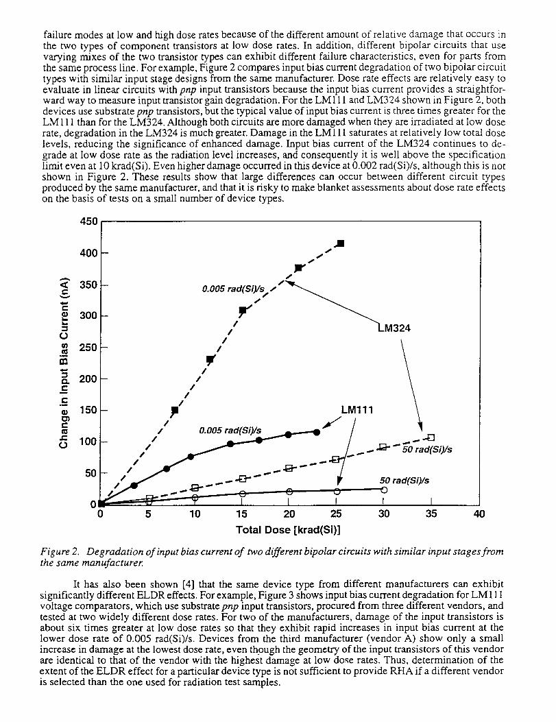
NEW RADIATION PHENOMENA IN ADVANCED DRAMS
Perhaps more than any other class of advanced microelectronic device, DRAMs represent a chal-lenge with regard to their insertion in space systems. Advanced DRAMs are particularly attractive for massstorage systems on board spacecraft and satellites, so that it is tempting to incorporate them in large memorydesigns. However, because the radiation tolerant space applications market is vanishingly small comparedto the commercial market for DRAMs, the designer is restricted to using commercial devices with little
chance of device or process modification to accommodate radiation requirements. Thus, it is imperative toperform extensive radiation testing to determine if the commercial device under consideration will meetspecific mission requirements. Unfortunately, DRAM advancements are proceeding so rapidly that by the
time one has expended considerable effort and money performing Single Event Effects (SEE) and TotalIonizing Dose (TID) effects radiation tests, the DRAM under test is obsolete and essentially unavailable. Inaddition, scaling effects in newer devices cao. render radiation test results inapplicable to the latest DRAMtechnology. Add to this the new phenomena we discuss below and one is faced with a very challengingassurance problem for space applications of advanced DRAMs.
In the past few years, several studies [16-26] of DRAMs and SRAMs have revealed new radiationeffects phenomena that can affect solid state memory performance in radiation environments. As we willshow, technology advancements in the form of scaling to achieve reduced feature sizes and greater memorycell densities will probably exacerbate these effects.
State-of-the-art DRAMs are complex devices that often incorporate much more circuitry than simpleDRAM cells and the necessary peripheral circuitry for accessing and writing/reading these cells. In par-ticular, several operating modes may be built into the device in order to facilitate various test modes of
operation. Normally a command sequence is used to place the DRAM in a test mode, but recent SEEtesting [16] has revealed that an energetic heavy ion can throw the DRAM out of normal operating modeand into one of its test modes if the particle hits the circuit device that controls operating mode. These socalled Single Event Functionality Interrupt (SEFI) events render the device inoperable until it is placedback in normal mode by specific commands. Unlike a traditional Single Event Upset (SEU), which resultsin a single error in one logic element, SEHs manifest themselves as bursts of large numbers of errors dueto a single particle hit. Thus, although the interaction cross section for a SEFI is less than that for a typicalSEU, the effect has much greater impact on DRAM functionality. Fortunately, the effect is not permanentand can be removed by commanding the device to reenter standard operating mode. Thus, it is not perma-nently catastrophic in contrast with an important new class of single event hard errors we will discuss next.
During the last few years, several laboratories have observed single particle induced errors whichare permanent in nature in contrast with the more traditional SEU event which is a temporary change in
logic state of a circuit logic element. These "stuck bits" or "hard errors" remain in the device despite powercycling or reloading of a memory. More recently, work at various heavy ion accelerators [ 18-21,23-25] hasled to a tentative identification of the nature of these hard errors. Earlier work [18,19] suggested that theonly mechanism for hard error formation was a so-called "microdose" effect. This effect is the singleparticle/single transistor equivalent of a Co 6°or total dose irradiation, and is due to microscopic ionizationdamage from the passage of a single ion (or a small number of ions) within the transistor gate region. As theresult of continued scaling, transistors in advanced memories are now small enough so that a single ion candeposit enough ionizing energy to create the equivalent of a "total dose" effect within a single transistor.
This effect is primarily important for DRAMs or 4-transistor memory cell SRAMs that use dynamic stor-age, but is not expected to be significant for random logic or 6-transistor memory cell SRAMs. In addition,it has been established that at least some fraction of these microdose-induced hard errors will anneal, as
one might expect based on the characteristics of typical TID damage. Thus, these hard errors will recoverslowly, unlike the second type described below.
The second mechanism causes catastrophic shorting of the gate oxide in the specific transistor thatis struck by the energetic heavy ion [21]. It is attributed to gate rupture, and occurs because the high charge
density produced by the ion track reduces the electric field needed to cause dielectric breakdown of thegate inslator. The result is destructive, permanent damage caused by the combination of applied field andheavy ion strike. Similar effects have been studied for several years in power MOSFETs [14,15], but theyhave only recently been observed for lower voltage transistors in VLSI devices. Theoretically, gate rupturecan occur for random logic as well as memories, and may prevent the use of extremely scaled (miniatur-ized) devices in space. Note also that this effect is similar to the anti-fuse SEDR effect described above forFPGAs.

Heavyion data,shownin Figure7, takenoncommercial4-Mb DRAMs illustrates the strikingdifference between the two hard error mechanisms [21 ]. The distribution of lost bits as a function of DRAM
retention time for iodine bombardment agrees with observations after total dose irradiation in which thedistribution "walks" to the left in Figure 7 so that fewer and fewer bits have long retention times above thepart specification of 360 ms at 45°C. In contrast, for gold bombardment two different types of data areobserved. In addition to results similar to the iodine induced microdose distribution, the Au also causes
permanent damage that is characterized by extremely short retention times, essentially zero. As in the caseof power MOSFET gate rupture and the FPGA rupture effect described above, the angular dependence ofthe permanent damage is unlike traditional SEU. The natural separation into "lost ones" and "lost zeros" isalso suggestive of a permanent'effect that requires a bias on the transistor to cause damage. This second
mechanism is particularly important for several reasons: 1) it is permanent and does not anneal so that overthe course of a long mission, these errors will accumulate; 2) this effect causes catastrophic failure of thetransistor in which it occurs; 3) this type of hard error could occur in any MOS transistor with bias on the
gate so that it will also affect microprocessors and random logic circuits which are not amenable to soft-ware-based error detection and correction; and 4) this effect.will become worse with continued part scaling
that is sure to take place as circuits with greater and greater performance are brought into the market place.
I--oO0..J
u.
o
W
Z
IO6__
m
B
105- ---
104_--=
103 =---
102--
10----
1
' ''''"1 '' ''""1 ' ''''"'1 ' '''""1 ' ''''"'1 ' '''"'I ' ''''"1 '' ''"_GOLD (NORMAL INCIDENCE) _B _;_
NOTETHATTHEREARE fr
(all lost zeros) i
I OKI 4Mb DRAM (std) I
I
Spec (360 ms)-._.._..._-='_1
II
Measurements at 45°C !I
, ,,),),)I , I ,,,i,d ) , ,,,,,,,I , , I,l ,,,,,,,I10-5 10-4 10,3 10-2 10-1 100 101
RETENTION TIME (see)
---,:_
I t II IIII
lO2
Figure 7. Retention time distributions for iodine (LET = 0.6 pC/prn) and gold (LET = 0.8 pC/p.m)bombarded OK! 4 Mb DRAMs.
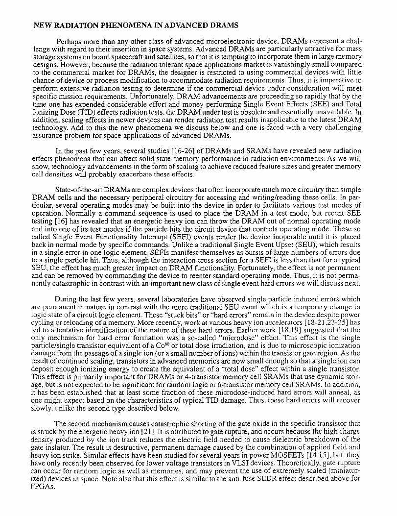
To illustrate the potentially negative effects of the permanent hard error mechanism on scaled de-vices, JPL examined a second set of 4 Mb DRAMs from the same manufacturer that had 20% smaller
dimensions and thinner gate oxides. The scaled devices were more sensitive to the permanent damageeffect in that the effect was observed for iodine at a lower LET than for gold. The damage thresholds,
expressed in terms of the linear charge density deposited by the ions, are shown in Figure 8. The dashedline shows a prediction of the effect of future scaling changes, assuming that the threshold for gate rupturevaries as the reciprocal of the square of the electric field across the oxide, using oxide fields typical of high
speed scaling techniques.
In order to understand the implications of these results, one must take into account the distribution
of the ions making up galactic cosmic rays (GCRs), which decrease rapidly for high linear charge densi-ties. Above 0.3 pC/gin, the distribution falls abruptly by more than three orders of magnitude, the so-callediron ion threshold that is characteristic of the GCR spectrum. These results have been used to calculate thecatastrophic hard-error rate for devices with different feature sizes, as shown in Figure 9. The error rate in
Figure9representsthenumberof faileddevicesfor aVLSI circuit with approximatelyonemillion transis-tors.Thereis apronounceddifferencein theerrorratefor thehighspeedscalingapproachversusthelowpowerscalingmethodbecauseof thedifferencesin theway thegateoxidefield scalesin eachcase.Thevery rapid increasein the errorrate of the high speedscalingcurveoccurswhenthe thresholdchargedensityfalls below0.3 pC]gm,wherethereis a largejump in the numberof GCR particles.The curvesuggeststhatit will beverydifficult to usedeviceswith0.25t.krnfeature size because of the hard error limit,and that devices optimized for low power operation will have a much lower error rate in space applications.
0.25 I I I I I I
0.20
04"-" 0.15>
o
cq
u._ 0.10
Figure 8.
0.05
High-SpeedScaling
Experimental Results for4 Mbit DRAMs (5V power supply)
//_0.8_. 0.8 p.m
/..e /
0.4 _ //0.5 p.mI
0.25 p.m //
-I Cfmic-ray
"Iron Threshold"±
o _ I I I I I0.2 02 0.4 05 0.6 0.7 0.8 0.9
Linear Charge Density from Heavy Ion (pC/IJ.m)
Effect of device scaling (miniaturization) on hard error threshold for various feature sizes.
100000
10O00
<_ lOOOo
o_
t-
•_ 100i..-
lO,2o
1ouJ
0.1
0.01
I I I i
Large increase below 0.25 pm _._---_-,Loccurs because of the f/
distributi:2e°rfCe°smic'ra_y S _/
;& [ i/soa,in j
S =.B/_ Low
I I I I2 1 0.5 0.25 0.13 0.065
Feature Size (p.m)
Figure 9. Hard errors induced by cosmic rays for a 1-M transistor array as feature sizes are reduced.
IMPLICATIONS FOR EMERGING TECHNOLOGIES
Thus far, we have discussed important new radiation effects phenomena that will affect the radia-tion susceptibility of advanced rnicroelectronic and electromechanical systems in spacecraft and satellites.In addition, we have seen that advances in performance in traditional electronic technologies, such asDRAMs and microprocessors, which are achieved through scaling (miniaturization) of feature sizes, willresult in devices and circuits that are more sensitive to radiation effects. We wish to close our discussion byemphasizing that c_re must also be taken in the insertion of new, emerging technologies in space systemsin order to avoid radiation effects problems that may jeopardize mission success. In many cases, the use ofconcurrent engineering to examine potential radiation problems at early design stages will catch problemsbefore they reach a stage that will result in Considerable cost and schedule penalties to repair. One exampleconcerns the insertion of fiber optic data links in high data rate space applications. The use of fibers and Sidetectors at the so called "first window" at a wavelength of approximately 850 nm is inappropriate for aradiation environment because these fibers and detectors are more sensitive to radiation than the fibers and
III-V-based detectors used at the second (1.3 I.tm) and third ( 1.55/am) windows.
As we have noted above, many MEMS technologies involve the use of insulators in some fashion,and these insulators may have electric fields across them. In such cases, ionizing radiation and heavy,energetic ions can alter the operating characteristics of devices that depend on these insulator structures forfunctional operation. In addition, in most MEMS the core element, such as a microaccelerometer ormicrogyro, is on a chip that also includes a variety of more traditional electronic devices. Thus, eventhough the heart of the MEMS may not be sensitive to radiation, it is possible that the MEMS functionalitywill be disrupted in a radiation environment. In the rush to fly these powerful new miniaturized technolo-gies we must not forget that their success can be jeopardized by radiation effects that can sometimes occurin the MEMS themselves, or in the more mundane technology devices that facilitate the operation of theMEMS.
REFERENCES
1. R. Nowlin, D. Fleetwood and R. Schrimpf, "Saturation of the dose rate response of bipolar transistors
below 10 rad(SiO2)/s: implications for hardness assurance", IEEE Trans. Nuc. Sci. NS-41, 2637 (1994).
2. S. McClure, R. Pease, W. Will and G. Perry, "Dependence of total dose response of bipolar linearmicrocircuits on applied dose rate", IEEE Trans. Nuc. Sci. NS-41, 2544 (1994).
3. D. Fleetwood; S. Kosier, R. Nowlin, R. Schrimpf, R. Reber, Jr., M. DeLaus, R Winokur, A. Wei, W.Combs and R. Pease, "Physical mechanisms contributing to enhanced bipolar gain de_adation at low doserates", IEEE Trans. Nuc. Sci. NS-41, 1871 (1994).
4. A. Johnston, G. Swift and B. Rax, "Total dose effects in conventional bipolar transistors and integratedcircuits", IEEE Trans. Nuc. Sci. NS-41, 2452 (1994).
5. D. Schmidt, R. Graves, R. Schrimpf, D. Fleetwood, R. Nowlin and W. Combs, "Comparison of ionizingradiation induced gain degradation in lateral, substrate, and vertical PNP BJTs", presented at the 32ndInternational Nuclear and Space Radiation Effects Conf., Madison, WI, July, 1995; to be published inIEEE Trans. Nuc. Sci. NS-42 (1995).
6. A. Johnston, B. Rax and C. Lee, "Enhanced damage in linear bipolar integrated circuits at low dose
rate", presented at the 32nd International Nuclear and Space Radiation Effects Conf., Madison, W-I, July,1995; to be published in IEEE Trans. Nuc. Sci. NS-42 (1995).
7. R. Graves, D. Schmidt, R. Schrimpf, D. Fleetwood, R. Nowlin, W. Combs, R. Pease and M. DeLaus,"Hardness assurance issues for lateral PNP bipolar junction transistors", presented at the 32nd Interna-tional Nuclear and Space Radiation Effects Conf., Madison, WI, July, 1995; to be published in IEEETrans. Nuc. Sci. NS-42 (1995).
8. A. Johnston, C. Lee, B. Rax and D. Shaw, "Using commercial semiconductor technologies in space",presented at the Third European Conf. On Radiation and Its Effects on Components and Systems (RADECS95), Arcachon, France, September, 1995.

9. R. Schrimpf, "Recent advances in understanding total dose effects in bipolar transistors", presented atthe Third European Conf. On Radiation and Its Effects on Components and Systems (RADECS 95), Arcachon,
France, September, 1995.
10. J. Bosc, G. Sarrabayrouse and F. Guerre, "Total dose effects on elementary transistors of a comparator
in bipolar technology", presented at the Third European Conf. On Radiation and Its Effects on Compo-nents and Systems (RADECS 95), Arcachon, France, September, 1995.
11. R. Katz, R. Barto, R McKerracher, B. Carkhuff and R. Koga, "SEU hardening of field programmable
gate arrays (FPGAs) for space applications and device characterization", IEEE Trans. Nuc. Sci. NS-41_,2179 (1994).
12. R. Katz, G. Swift and R. Barto, ".Anti-fuse reliability in the heavy ion environment", presented at the32nd International Nuclear and Space Radiation Effects Conf., Madison, WI, July, 1995.
13. G. Swift and R. Katz, "An experimental survey of heavy ion induced dielectric rupture", presented atthe Third European Conf. On Radiation and Its Effects on Components and Systems (RADECS 95), Arcachon,
France, September, 1995.
14. H. Joseph, "Radiation-induced effects on special superlarge n-channel power MOSFETs for spaceapplications", p. 128 in Proc. of First European Conf. On Radiation and Its Effects on Components andSystems (RADECS 91) (1992).
15. D. Nichols, J. Coss and K. McCarty, "Single event gate rupture in commercial power MOSFETs", p.462 in Proc. of Second European Conf. On Radiation and Its Effects on Components and Systems (RADECS93) (1994).
16. G. Swift, L. Smith and H. Schafzahl, "Single event functionality interrupt: a new failure mode forsemiconductor memories", presented at the 9th Single Event Effects Symposium, Manhattan Beach, CA,
April, 1994.
17. R. Koga, W. Crain, K. Crawford, D. Lau, S. Pinkerton, B. Yi and R. Chitty, "On the suitability of non-hardened high density SRAMs for space", IEEE Trans. Nuc. Sci. NS-38, 1507 (1991).
18. C. Dufour, R Gamier, T. Carriere, J. Beaucour, R. Ecoffet and M. Labrunee, "Heavy ion induced singlehard errors on submicronic memories", IEEE Trans. Nuc. Sci. NS-39, 1693 (1992).
19. T. Oldham, K. Bennett, J. Beaucour, T. Camere, C. Polvey and R Gamier, "Total dose failures inadvanced electronics from single ions", IEEE Trans. Nuc. Sci. NS-40, 1820 (1993).
20. S. Duzellier, D. Falguere and R. Ecoffet, "Protons and heavy ions induced stuck bits on large capacityRAMs", p. 468 in Proc. of Second European Conf. On Radiation and Its Effects on Components andSystems (RADECS 93) (1994).
21. G. Swift, D. Padgett and A. Johnston, "A new class of single event hard errors", IEEE Trans. Nuc. Sci.NS-41, 2043 (1994).
22. D. Shaw, G. Swift, D. Padgett and A. Johnston, "Radiation effects in five volt and advanced lowervoltage DRAMs", IEEE Trans. Nuc. Sci. NS-41, 2452 (1994).
23. R Calvel, R Lamothe, C. Barillot, R. Ecoffet, S. Duzellier and E. Stassinopoulos, "Space radiation
evaluation of 16 Mbit DRAMs for mass memory applications", IEEE Trans. Nuc. Sci. NS-41., 2267 (1994).
24. D. Shaw, G. Swift, D. Padgett and A. Johnston, "Radiation evaluation of an advanced 64 Mb, 3.3 VDRAM and insights into the effects of scaling on radiation hardness", presented at the 32nd InternationalNuclear and Space Radiation Effects Conf., Madison, WI, July, 1995; to be published in IEEE Trans. Nuc.Sci. NS-42 (1995).
25. R. Harboe-Sorensen, S. Fraenkel, R. Muller and T. Braunschweig, "Heavy ion, proton and Co-60radiation evaluation of 16 Mbit DRAM memories for space application", presented at the 32rid Interna-
tional Nuclear and Space Radiation Effects Conf., Madison, WI, July, 1995; to be published in IEEETrans. Nuc. Sci. NS-42 (1995).
26. A. Johnston, G. Swift and D. Shaw, "Impact of CMOS scaling on single event hard errors in space
systems", presented at the 1995 Symposium on Low Power Electronics, San Jose, CA, October, 1995, p.88 in Digest of Technical Papers from 1995 SLPE Conf., October, 1995.