the idea architecture-focused fpga soft processor€¦ · comrades, thinh, khoa, sanjeev, lianlian,...
TRANSCRIPT

NANYANG TECHNOLOGICAL UNIVERSITY
The iDEA Architecture-Focused FPGA
Soft Processor
Cheah Hui Yan
School of Computer Engineering
A thesis submitted to Nanyang Technological University
in partial fulfilment of the requirements for the degree of
Doctor of Philosophy
2016

i
Acknowledgements
This thesis has benefited tremendously from the generosity and sacrifice of many
others: my advisors, Suhaib Fahmy and Nachiket Kapre; my fellow students with
whom I had many thought-provoking discussions, Fredrik and Liwei; my confi-
dant and moral compass, Vijeta and Supriya; my phenomenal technical support,
Jeremiah; my patient draft readers, Nitin and Yupeng; and my friends and fellow
comrades, Thinh, Khoa, Sanjeev, Lianlian, Sid, Sharad, Abhishek Jain, Abhisek
Ambede, Sumedh, and Siew Kei. Also not forgetting the mentor who helped me
get started in research, Douglas Maskell. Special thanks to my parents, my Guru,
Sangha, and the FPGA community. Most of all, I want to thank Seong for his
unwavering support and attention.

Contents
List of Abbrevations xv
1 Introduction 1
1.1 Motivation . . . . . . . . . . . . . . . . . . . . . . . . . . . . . . . . 4
1.2 Research Goals . . . . . . . . . . . . . . . . . . . . . . . . . . . . . 5
1.3 Contributions . . . . . . . . . . . . . . . . . . . . . . . . . . . . . . 6
1.4 Organization . . . . . . . . . . . . . . . . . . . . . . . . . . . . . . 7
1.5 Publications . . . . . . . . . . . . . . . . . . . . . . . . . . . . . . . 8
2 Background 9
2.1 FPGA Architecture . . . . . . . . . . . . . . . . . . . . . . . . . . . 9
2.1.1 Configurable Logic Blocks . . . . . . . . . . . . . . . . . . . 10
2.1.2 Embedded Blocks . . . . . . . . . . . . . . . . . . . . . . . . 11
2.1.2.1 BRAMs . . . . . . . . . . . . . . . . . . . . . . . . 12
2.1.2.2 DSPs . . . . . . . . . . . . . . . . . . . . . . . . . 12
2.1.2.3 Processors . . . . . . . . . . . . . . . . . . . . . . . 13
2.2 FPGA Design Flow . . . . . . . . . . . . . . . . . . . . . . . . . . . 13
2.3 Soft Processors . . . . . . . . . . . . . . . . . . . . . . . . . . . . . 15
2.3.1 Advantages Over Hard Processor . . . . . . . . . . . . . . . 16
2.3.2 Advantages Over Custom Hardware . . . . . . . . . . . . . . 17
2.3.3 Commercial and Open-source Soft processors . . . . . . . . . 18
2.3.4 Customizing Soft Processor Microarchitecture . . . . . . . . 19
2.4 Related Work . . . . . . . . . . . . . . . . . . . . . . . . . . . . . . 20
2.4.1 Single Processors . . . . . . . . . . . . . . . . . . . . . . . . 20
2.4.2 Multithreaded . . . . . . . . . . . . . . . . . . . . . . . . . . 23
2.4.3 Vector . . . . . . . . . . . . . . . . . . . . . . . . . . . . . . 24
2.4.4 VLIW . . . . . . . . . . . . . . . . . . . . . . . . . . . . . . 27
2.4.5 Multiprocessors . . . . . . . . . . . . . . . . . . . . . . . . . 28
2.4.6 DSP Block-Based . . . . . . . . . . . . . . . . . . . . . . . . 31
2.5 Summary . . . . . . . . . . . . . . . . . . . . . . . . . . . . . . . . 33
3 DSP Block as an Execution Unit 35
3.1 Evolution of the DSP Block . . . . . . . . . . . . . . . . . . . . . . 36
3.2 Multiplier and Non-Multiplier Paths . . . . . . . . . . . . . . . . . 39
3.3 Executing Instructions on the DSP48E1 . . . . . . . . . . . . . . . 40
ii

CONTENTS iii
3.3.1 Multiplication . . . . . . . . . . . . . . . . . . . . . . . . . . 40
3.3.2 Addition . . . . . . . . . . . . . . . . . . . . . . . . . . . . . 41
3.3.3 Compare . . . . . . . . . . . . . . . . . . . . . . . . . . . . . 43
3.3.4 Shift . . . . . . . . . . . . . . . . . . . . . . . . . . . . . . . 44
3.4 Balancing the DSP Pipelines . . . . . . . . . . . . . . . . . . . . . . 45
3.5 Iterative Computation on the DSP Block . . . . . . . . . . . . . . . 47
3.6 Summary . . . . . . . . . . . . . . . . . . . . . . . . . . . . . . . . 50
4 iDEA: A DSP-based Processor 51
4.1 Introduction . . . . . . . . . . . . . . . . . . . . . . . . . . . . . . . 51
4.2 Processor Architecture . . . . . . . . . . . . . . . . . . . . . . . . . 52
4.2.1 Overview . . . . . . . . . . . . . . . . . . . . . . . . . . . . 52
4.2.2 Instruction and Data Memory . . . . . . . . . . . . . . . . . 53
4.2.3 Register File . . . . . . . . . . . . . . . . . . . . . . . . . . . 55
4.2.4 Execution Unit . . . . . . . . . . . . . . . . . . . . . . . . . 56
4.2.5 Other Functional Units . . . . . . . . . . . . . . . . . . . . . 58
4.2.6 Overall Architecture . . . . . . . . . . . . . . . . . . . . . . 58
4.3 Instruction Set Format and Design . . . . . . . . . . . . . . . . . . 59
4.3.1 Input Mapping . . . . . . . . . . . . . . . . . . . . . . . . . 60
4.3.2 DSP Output . . . . . . . . . . . . . . . . . . . . . . . . . . . 63
4.4 Hardware Implementation . . . . . . . . . . . . . . . . . . . . . . . 64
4.4.1 Area and Frequency Results . . . . . . . . . . . . . . . . . . 64
4.5 Software Toolchain . . . . . . . . . . . . . . . . . . . . . . . . . . . 66
4.5.1 Assembly Converter . . . . . . . . . . . . . . . . . . . . . . 68
4.5.2 iDEA Simulator . . . . . . . . . . . . . . . . . . . . . . . . . 68
4.5.3 Benchmarks . . . . . . . . . . . . . . . . . . . . . . . . . . . 69
4.6 Execution Results . . . . . . . . . . . . . . . . . . . . . . . . . . . . 70
4.6.1 NOPs and Pipeline Depth . . . . . . . . . . . . . . . . . . . 70
4.6.2 Execution Time . . . . . . . . . . . . . . . . . . . . . . . . . 71
4.6.3 Multiply-Add Instructions . . . . . . . . . . . . . . . . . . . 73
4.7 Summary . . . . . . . . . . . . . . . . . . . . . . . . . . . . . . . . 75
5 Composite Instruction Support in iDEA 77
5.1 Introduction . . . . . . . . . . . . . . . . . . . . . . . . . . . . . . . 77
5.2 Potential of Composite Instruction . . . . . . . . . . . . . . . . . . 78
5.3 Related Work . . . . . . . . . . . . . . . . . . . . . . . . . . . . . . 79
5.4 Intermediate Representation . . . . . . . . . . . . . . . . . . . . . . 81
5.5 SAT Non-Overlapping Analysis . . . . . . . . . . . . . . . . . . . . 84
5.5.1 Pseudo-boolean Optimization . . . . . . . . . . . . . . . . . 85
5.5.2 Constructing the Conflict Graph . . . . . . . . . . . . . . . 86
5.5.3 Applying the Pseudo-boolean Formula . . . . . . . . . . . . 87
5.5.4 SAT Experimental Framework . . . . . . . . . . . . . . . . . 88
5.6 Static Analysis of Dependent Instructions . . . . . . . . . . . . . . 90
5.7 Dynamic Analysis of Composite Instructions . . . . . . . . . . . . . 94

CONTENTS iv
5.7.1 Dynamic Occurrence . . . . . . . . . . . . . . . . . . . . . . 94
5.7.2 Speedup . . . . . . . . . . . . . . . . . . . . . . . . . . . . . 97
5.8 Hardware Implementation . . . . . . . . . . . . . . . . . . . . . . . 98
5.9 Summary . . . . . . . . . . . . . . . . . . . . . . . . . . . . . . . . 102
6 Data Forwarding Using Loopback Instructions 103
6.1 Introduction . . . . . . . . . . . . . . . . . . . . . . . . . . . . . . . 103
6.2 Data Hazards in a Deeply Pipelined Soft Processor . . . . . . . . . 104
6.3 Related Work . . . . . . . . . . . . . . . . . . . . . . . . . . . . . . 106
6.4 Managing Dependencies in Processor Pipelines . . . . . . . . . . . . 107
6.5 Implementing Data Forwarding . . . . . . . . . . . . . . . . . . . . 109
6.5.1 External Data Forwarding . . . . . . . . . . . . . . . . . . . 110
6.5.2 Proposed Internal Forwarding . . . . . . . . . . . . . . . . . 110
6.5.3 Instruction Set Modifications . . . . . . . . . . . . . . . . . 111
6.6 DSP Block Loopback Support . . . . . . . . . . . . . . . . . . . . . 112
6.7 DSP ALU Multiplexers . . . . . . . . . . . . . . . . . . . . . . . . . 113
6.8 NOP-Insertion Software Pass . . . . . . . . . . . . . . . . . . . . . 114
6.9 Experiments . . . . . . . . . . . . . . . . . . . . . . . . . . . . . . . 115
6.9.1 Area and Frequency Analysis . . . . . . . . . . . . . . . . . 117
6.9.2 Execution Analysis . . . . . . . . . . . . . . . . . . . . . . . 120
6.10 Summary . . . . . . . . . . . . . . . . . . . . . . . . . . . . . . . . 124
7 Conclusions and Future Work 127
7.1 Future Work . . . . . . . . . . . . . . . . . . . . . . . . . . . . . . . 130
A Instruction Set 135
B DSP Configurations 137
Bibliography 139

ABSTRACT OF THE DISSERTATION
The iDEA Architecture-Focused FPGA Soft Processor
by
Cheah Hui YanDoctor of Philosophy
School of Computer Engineering
Nanyang Technological University, Singapore
The performance and power benefits of FPGAs have remained accessible primar-
ily to designers with strong hardware skills. Yet as FPGAs have evolved, they
have gained capabilities that make them suitable for a wide range of domains and
more complex systems. However, the low level, time-consuming hardware design
process remains an obstacle towards much wider adoption. An idea gaining some
traction recently is the use of soft programmable architectures built on top of the
FPGA as overlays, with compilers translating code to be executed on these archi-
tectures. This allows the use of strong compiler frameworks and also avoids the
bit-level cycle-level design required in RTL design. A key issue with soft over-
lay architectures is that when designed without consideration for the underlying
FPGA architecture, they suffer from significant performance and area overheads.
This thesis presents an FPGA architecture-focused soft processor built to demon-
strate the benefits of leveraging detailed architecture capabilities. It uses the
highly capable DSP blocks on modern Xilinx devices to enable a general purpose
processor that is small and fast. We show that the DSP48E1 blocks in Xilinx
Virtex-6 and 7-Series devices support a wide range of standard processor instruc-
tions that can be designed into the core of a processor we call iDEA. On recent
devices it can run close to the limit of 500MHz, while consuming considerably less
area than other soft processors. We conduct a detailed design space exploration
to identify the optimal pipeline depth for iDEA.
We then propose the use of composite instructions to improve performance through
better use of the DSP block, and show a speedup of up to 1.2× over a processor
without composite instructions. Finally, we show how a restricted forwarding
scheme that uses an internal DSP block accumulation path can eliminate some of
the dependency overheads in executing programs, achieving a 25% improvement
in execution time, compared to an alternative forwarding path implemented in the
logic fabric, which offers only a 5% improvement.

CONTENTS vi
We benchmark our processor with a range of representative benchmarks and anal-
yse it at the compiler, instruction, and cycle levels.

List of Figures
1.1 Comparison of FPGA design flows: (a) RTL-based (b) HLS-based(c) intermediate architecture . . . . . . . . . . . . . . . . . . . . . . 2
1.2 Abstracting FPGA heterogeneous logic elements. . . . . . . . . . . 3
1.3 Executing (a) single (b) composite and (c) loopback instructions iniDEA. . . . . . . . . . . . . . . . . . . . . . . . . . . . . . . . . . . 6
2.1 FPGA architecture. . . . . . . . . . . . . . . . . . . . . . . . . . . . 10
2.2 General architecture of a logic element (LE) inside a configurablelogic block (CLB). . . . . . . . . . . . . . . . . . . . . . . . . . . . 11
2.3 A Xilinx DSP Block with Multiplier and ALU (Arithmetic LogicUnit). . . . . . . . . . . . . . . . . . . . . . . . . . . . . . . . . . . 13
2.4 FPGA design process. . . . . . . . . . . . . . . . . . . . . . . . . . 14
3.1 Architecture of the DSP48E1. Main components are: pre-adder,multiplier and ALU. . . . . . . . . . . . . . . . . . . . . . . . . . . 39
3.2 (a) Multiplier and (b) non-multiplier datapath. . . . . . . . . . . . 40
3.3 Datapath for (a) multiply (b) multiply-add (c) multiply-accummulate 42
3.4 Datapath for addition. Extra register C0 to balance the pipeline. . 43
3.5 Datapath for compare. Pattern detect logic compares the value ofC and P. . . . . . . . . . . . . . . . . . . . . . . . . . . . . . . . . . 43
3.6 Datapath for shift. An extra shift LUT is required. . . . . . . . . . 44
3.7 Switching between multipy and add/subtract/logical path. Pathsare pipelined equally at 3 stages. . . . . . . . . . . . . . . . . . . . 46
3.8 Waveforms showing structural hazard of unbalanced pipeline depths 47
3.9 Implementing Chebyshev polynomial on FPGA. Polynomial equa-tion: T4[x] = 8x4 − 8x2 + 1 . . . . . . . . . . . . . . . . . . . . . . . 48
4.1 A RISC 5-cycle pipeline structure [1]. . . . . . . . . . . . . . . . . . 53
4.2 iDEA processor block diagram. . . . . . . . . . . . . . . . . . . . . 58
4.3 (a) 2-operand (b) 3-operand input map. . . . . . . . . . . . . . . . 62
4.4 Simulator and toolchain flow. . . . . . . . . . . . . . . . . . . . . . 67
4.5 Frequency and geomean wall clock time at various pipeline depths. . 71
4.6 Comparison of execution time of iDEA and MicroBlaze at maximumpipeline-depth configuration. . . . . . . . . . . . . . . . . . . . . . . 72
4.7 Execution time of iDEA relative to MicroBlaze. . . . . . . . . . . . 72
4.8 Relative execution time of benchmarks using composite instructions 74
vii

LIST OF FIGURES viii
5.1 Mapping a two-node subgraph to DSP block. Pre-adder is not de-picted. . . . . . . . . . . . . . . . . . . . . . . . . . . . . . . . . . . 78
5.2 Compiler flow. . . . . . . . . . . . . . . . . . . . . . . . . . . . . . . 81
5.3 (a) Control flow graph (b) Dependence graph for a multiply-addfunction. . . . . . . . . . . . . . . . . . . . . . . . . . . . . . . . . . 83
5.4 Modelling composite nodes into SAT formula. . . . . . . . . . . . . 87
5.5 Overlapping dependent nodes in adpcm basic block. . . . . . . . . . 89
5.6 Speedups resulting from composite instructions. . . . . . . . . . . . 98
5.7 Path for (a) single instructions (b) composite instructions. . . . . . 99
5.8 Number of composite instructions implemented for each benchmark 101
5.9 Resource utilization of individual CHSTONE benchmark hardwareimplementation . . . . . . . . . . . . . . . . . . . . . . . . . . . . . 101
5.10 Speedup of benchmarks in a 11-stage iDEA . . . . . . . . . . . . . 101
6.1 NOP counts as pipeline depth increases with no data forwarding. . 104
6.2 Dependencies for pipeline depths of 7, 8 and 9 stages. . . . . . . . . 105
6.3 Reduced instruction count with data forwarding. . . . . . . . . . . . 108
6.4 Forwarding configurations, showing how subsequent instruction cancommence earlier in the pipeline. . . . . . . . . . . . . . . . . . . . 109
6.5 Execution unit datapath showing internal loopback and externalforwarding paths. . . . . . . . . . . . . . . . . . . . . . . . . . . . . 112
6.6 Multiplexers selecting inputs from A, B, C and P. . . . . . . . . . . 113
6.7 Experimental flow. . . . . . . . . . . . . . . . . . . . . . . . . . . . 116
6.8 Frequency of different pipeline combinations with internal loopback. 117
6.9 Resource utilization of all pipeline combinations with internal loop-back. . . . . . . . . . . . . . . . . . . . . . . . . . . . . . . . . . . . 119
6.10 Resource utilization of highest frequency configuration for internal,external and no loopback. . . . . . . . . . . . . . . . . . . . . . . . 119
6.11 Frequency with internal loopback and external forwarding. . . . . . 120
6.12 IPC improvement when using internal DSP loopback. . . . . . . . . 122
6.13 IPC improvement when using external loopback. . . . . . . . . . . . 122
6.14 Frequency and geomean wall clock time with and without internalloopback enabled. . . . . . . . . . . . . . . . . . . . . . . . . . . . . 123
6.15 Frequency and geomean wall clock time on designs incorporatinginternal loopback and external forwarding. . . . . . . . . . . . . . . 123

List of Tables
2.1 Summary of related work in soft processors. . . . . . . . . . . . . . 32
3.1 Comparison of multiplier and DSP primitives in Xilinx devices. Re-fer to Figure 3.1 for architecture of the DSP48E1. . . . . . . . . . . 38
3.2 DSP48E1 dynamic control signals and static parameter attributes. . 41
3.3 Operations supported by the DSP48E1. . . . . . . . . . . . . . . . . 45
3.4 Parameter attributes for pipelining the DSP48E1 datapaths. . . . . 45
3.5 Comparing fixed and iterative Chebyshev polynomial implementation. 49
4.1 Maximum frequency of instruction and data memory in Virtex-6speed grade -2. . . . . . . . . . . . . . . . . . . . . . . . . . . . . . 54
4.2 Frequency for different pipeline configurations of the DSP48E1 inVirtex-6 speed grade -2 (with and without pattern detect enabled). 56
4.3 iDEA instruction set. . . . . . . . . . . . . . . . . . . . . . . . . . . 60
4.4 Port mapping for different arithmetic functions. . . . . . . . . . . . 61
4.5 Frequency and Area for iDEA and MicroBlaze. . . . . . . . . . . . . 65
4.6 10-stage iDEA in Artix-7, Kintex-7 and Virtex-7. . . . . . . . . . . 66
4.7 Number of NOPs inserted between dependent instructions. . . . . . 71
5.1 A 3-address LLVM IR. The basic block shows the sequence of in-structions to achieve multiply-add: load into register, perform op-eration, store back to memory. . . . . . . . . . . . . . . . . . . . . . 82
5.2 Objective function and constraints in OPB format for Sat4j solver. . 88
5.3 Dependent arithmetic operations of CHSTONE [2] benchmarks (LLVMintermediate representation). . . . . . . . . . . . . . . . . . . . . . . 90
5.4 CHSTONE benchmarks most frequently occurring node patterns.The nodes shl, ashr and lshr are shift left, arithmetic shift right andlogical shift right respectively. . . . . . . . . . . . . . . . . . . . . . 92
5.5 DSP sub-components of composite instructions. . . . . . . . . . . . 92
5.6 Distribution of iDEA legally fusable nodes in CHSTONE bench-marks (in percentage %). . . . . . . . . . . . . . . . . . . . . . . . . 93
5.7 iDEA overlapping and non-overlapping nodes. . . . . . . . . . . . . 94
5.8 Frequency of fusable instructions in each basic block. . . . . . . . . 95
5.9 Dynamic composite nodes of CHSTONE benchmarks. Dynamicallyrun using JIT compiler . . . . . . . . . . . . . . . . . . . . . . . . . 96
5.10 Frequency and area consumption of base processor with and withoutcomposite instructions (Pipeline length = 11). . . . . . . . . . . . . 99
ix

LIST OF TABLES x
6.1 Dynamic cycle counts with 11-stage pipeline with % of NOPs savings.108
6.2 Opcode of loopback instructions . . . . . . . . . . . . . . . . . . . . 111
6.3 Optimal combination of stages and associated NOPs at each pipelinedepth (WB = 1 in all cases) . . . . . . . . . . . . . . . . . . . . . . 118
6.4 Static cycle counts with and without loopback for a 10-cycle pipelinewith % savings. . . . . . . . . . . . . . . . . . . . . . . . . . . . . . 121
6.5 Dynamic cycle counts with and without loopback for a 10-cyclepipeline with % savings. . . . . . . . . . . . . . . . . . . . . . . . . 121
A.1 iDEA arithmetic and logical instructions. . . . . . . . . . . . . . . . 135
A.2 iDEA data transfer and control instructions. . . . . . . . . . . . . . 136
A.3 iDEA loopback and composite instructions. . . . . . . . . . . . . . . 136
B.1 DSP configurations in iDEA. . . . . . . . . . . . . . . . . . . . . . . 138

List of Abbrevations
ALU Arithmetic Logic Unit
ASIC Application Specific Integrated Circuit
CAD Computer Aided Design
CLB Configurable Logic Block
CMOS Complementary Metal Oxide Semiconductor
CRC Cyclic Redundancy Check
DSP Digital Signal Processing
DMA Direct Memory Access
FIR Finite Impulse Response
FPGA Field Programmable Gate Array
HDL Hardware Description Language
HLS High Level Synthesis
ISE Integrated Synthesis Environment
IR Intermediate Representation
LLVM Low Level Virtual Machine
LUT Look Up Table
MIMO Multiple-Input Multiple-Output
NOP No Operation
PAR Place-And-Route
PB Pseudo-Boolean
PC Program Counter
RISC Reduced Instruction Set Computing
RTL Register Transfer Level
SAT Satisfiability
XPS Xilinx Platform Studio
xi

Chapter 1
Introduction
The past few decades have seen enormous progress in the technology of Field
Programmable Gate Arrays (FPGAs). The ability to design custom datapaths
to maximize exploitation of parallelism in a wide variety of applications allows
them to offer orders of magnitude improved computational efficiency over software
running on processors. Despite the speed, area and power benefits, many designs
fail to fully harness the performance advantages offered by modern FPGAs. A
fundamental obstacle to this design limitation is the low-level hardware design
complexity. When developing for FPGAs designers seeking performance design a
cycle-by-cycle description at the register transfer level (RTL), which is cumbersome
and time-consuming (Refer Figure 1.1 (a)). Overcoming this drawback require
methods to “hide” away low-level FPGA details, allowing designers to design their
applications at a higher level of abstraction.
High level synthesis is one approach undergoing intense research effort at present.
This involves developing tools that can translate high level software code descrip-
tions of algorithms into hardware, with parallelism extracted automatically. This
allows designers to focus more on the trade-off between performance and area, and
to work with more familiar software design tools in functional stages of the design.
However, high-level synthesis does not address all aspects of the design complexity
obstacle, since they produce generic RTL that must still be implemented using the
standard vendor tools, entailing very long compile times.
1

Chapter 1 Introduction 2
C Design
High-Level Synthesis
RTL Design
Synthesis
FPGAFPGA
RTL Design
C Design
C Compiler
MapPlace-n-Route
SynthesisMap
Place-n-Route
FPGA
RTL Intermediate Architecture
SynthesisMap
Place-n-Route
ArchitectureSpecification
Architecture Generator
SW Program Files
(a) (b) (c)
Figure 1.1: Comparison of FPGA design flows: (a) RTL-based (b) HLS-based(c) intermediate architecture
Another possible approach is to use a layer of pre-built soft structures called an
overlay. Overlays are implemented on top of the FPGA fabric, and are generally
composed of arrays of programmable compute units. Hence, the overlay serves
as an intermediate fabric [3] upon which the desired application is built (Refer
Figure 1.1 (c)). Overlaying a compute architecture on top of the FPGA offers the
benefits of easier programmability and mapping, while still retaining the benefit of
flexibility through possible re-implementation of the architecture when required.
However, generalized structures such as overlays typically suffer from performance
and area overheads, due to their coarser granularity. Overheads can also be at-
tributed to the lack of consideration for the underlying FPGA architecture during
the overlay design process [4].
An overlay is constructed small processing elements that represent compute units,
and a general routing fabric to allow them to communicate. Some overlays are
statically configured with each processing element only performing a single oper-
ation and data flowing through the overlay [5]. Others have processing elements
that are each soft processors (Figure 1.2). Parallel software can be deployed to
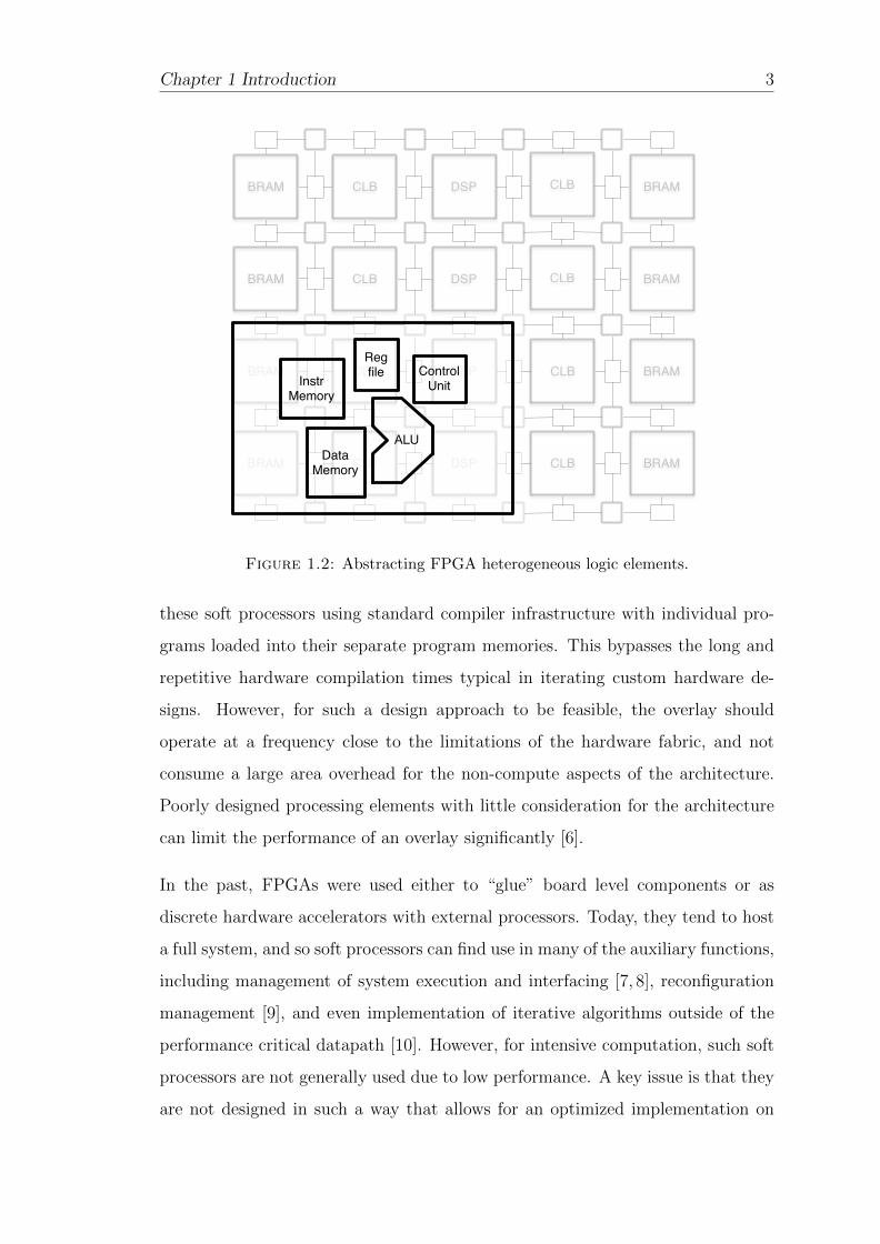
Chapter 1 Introduction 3
BRAM CLB DSP BRAM
BRAM CLB DSP CLB BRAM
CLB
BRAM CLB DSP CLB BRAM
BRAM CLB DSP CLB BRAM
RegfileInstr
Memory
DataMemory
Control Unit
ALU
Figure 1.2: Abstracting FPGA heterogeneous logic elements.
these soft processors using standard compiler infrastructure with individual pro-
grams loaded into their separate program memories. This bypasses the long and
repetitive hardware compilation times typical in iterating custom hardware de-
signs. However, for such a design approach to be feasible, the overlay should
operate at a frequency close to the limitations of the hardware fabric, and not
consume a large area overhead for the non-compute aspects of the architecture.
Poorly designed processing elements with little consideration for the architecture
can limit the performance of an overlay significantly [6].
In the past, FPGAs were used either to “glue” board level components or as
discrete hardware accelerators with external processors. Today, they tend to host
a full system, and so soft processors can find use in many of the auxiliary functions,
including management of system execution and interfacing [7, 8], reconfiguration
management [9], and even implementation of iterative algorithms outside of the
performance critical datapath [10]. However, for intensive computation, such soft
processors are not generally used due to low performance. A key issue is that they
are not designed in such a way that allows for an optimized implementation on

Chapter 1 Introduction 4
FPGAs. This not only affects performance, but many powerful features of the
FPGA heterogeneous logic resources are under-utilized. Consider the LEON3 [11]
soft processor: implemented on a Virtex-6 FPGA with a fabric that can support
operation at over 400 MHz, it only achieves a clock frequency of close to 100 MHz.
One key processing element in the FPGA, that has motivated and enabled the work
presented throughout this thesis, is the DSP block [12]. Unlike general purpose
reconfigurable logic, the DSP block is designed in silicon specifically to perform
arithmetic operations. The DSP block can support a large range of arithmetic
configurations, many of which can be modified at run-time on a cycle-by-cycle
basis, by modifying the control signals. DSP blocks are more power efficient,
operate at higher frequency, and consume less area then the equivalent operations
implemented using the fabric logic. As such, they are heavily used in the pipelined
datapaths of computationally intensive applications [13,14]. However, studies have
shown that DSP block inference by the synthesis tools can be sub-optimal [15],
and the dynamic programmability feature is not mapped except in very restricted
cases. As the number of DSP blocks on modern devices increases, finding ways to
use them efficiently outside of their core applications domain becomes necessary.
1.1 Motivation
The work in this thesis attempts to demonstrate the quantitative benefits of an
architecture-driven soft processor design. Modern FPGAs contain a variety of hard
blocks that have been optimized to offer high frequency operation while consuming
low area and power. Relying on implementation tools to maximize their use does
not always result in favourable implementations.
We present the iDEA FPGA soft processor that has been built and tailored around
the DSP48E1 block present in all modern Xilinx FPGAs. This block is designed
to enable the implementation of digital signal processing (DSP) structures at high
speed and with minimal additional logic. More importantly, the DSP48E1 offers
dynamic flexibility in the types of operations it executes. We show how this can be

Chapter 1 Introduction 5
harnessed to build a highly capable and small processor that operates at close to
the performance limits of this hard block, offering a processor that can be applied
in a wide variety of scenarios.
1.2 Research Goals
Generally DSP blocks offer the most benefit when mapping DSP applications.
However, as an abundant resource on modern FPGAs, it is worth investigating
how they can be used efficiently in a wider variety of applications to offer a higher
level software programmable compute unit. In this thesis, we answer the following
questions:
1. Can we use the dynamic programmability of modern DSP blocks to extend
their applicability beyond fixed-function custom DSP applications?
2. How do we build a fast, efficient soft processor considering the underlying
architecture of modern FPGAs particularly DSP blocks?
3. How do we exploit the components of a DSP block to further enhance the
performance of the processor for general embedded applications?
To answer the first question we implement a full DSP-based soft processor called
iDEA (DSP Extension Architecture) on a Xilinx Virtex-6 FPGA. We show that
a DSP block can support a wide range of standard processor instructions which
can be designed into the execution unit of a basic processor with minimal logic
usage. For the second question, we develop a parametric design of the iDEA
soft processor to allow variable pipeline depths and customization of individual
processor stages together with the embedded blocks. We also incorporate the
capability to remove datapath and hardware logic for unused instructions. Finally,
we propose a novel forwarding scheme and develop a framework to evaluate the
potential for augmented instructions from embedded benchmarks.

Chapter 1 Introduction 6
Register Register
Register Register Register
Register Register
Register
Register
Op 3
Op 1
Op 1
Op 1Op 2
Op 2
Op 2
Figure 1.3: Executing (a) single (b) composite and (c) loopback instructionsin iDEA.
1.3 Contributions
This thesis shows how to design, optimize, and implement a parametric, DSP
block based soft processor on a modern FPGA. Figure 1.3 shows the high level
conceptual roles of the DSP block as an execution unit in our soft processor. The
contributions of this thesis include:
1. iDEA Soft Processor: We deliver a functional DSP-based (single DSP
block) soft processor capable of performing general purpose instructions. We
exploit the dynamic control signals of the DSP block to switch between dif-
ferent arithmetic operations at runtime. We demonstrate the area-efficiency
of this processor over an equivalent LUT-based processor at 32% fewer reg-
isters and 59% fewer LUTs. We show the 10-stage 32-bit iDEA processor
can offer comparable performance to the Xilinx MicroBlaze while occupying
57% less LUT area. A full design-space exploration of the iDEA architecture
is also presented.
2. Composite Instructions: We improve the use of DSP block sub-components
by combining multiple arithmetic operations into single instructions. We de-
velop a framework to identify and select composite instructions: first through
identification of dependent arithmetic operations, followed by a pseudo-
boolean optimization model to select the optimal number of composite in-
structions. We show that utilizing the DSP pre-adder in combination with

Chapter 1 Introduction 7
multiplier or ALU can improve execution time of a set of benchmarks by as
much as 15% with less than a 1% increase in logic utilization.
3. Loopback Instructions: We demonstrate a way to use a DSP block fea-
ture to overcome the long dependency window resulting from iDEA’s deep
pipeline. We show a detailed comparison between a DSP-internal and DSP-
external loopback paths. We demonstrate that internal loopback forwarding
using the DSP block accumulate path can improve execution time for a set
of benchmarks by 25% at the cost of 3% increase in logic utilization over no
forwarding.
1.4 Organization
This thesis is organized as follows: Chapter 2 presents background on FPGA archi-
tecture, modern hard blocks, and the design flow. It then reviews related work on
soft processors including commercial and academic designs designed for use in sin-
gle and multi-processor arrangements. Chapter 3 presents the architecture of the
DSP48E1 hard block found in modern Xilinx FPGAs, its processing capabilities,
dynamic configurability, and how this can support successive operations. Chap-
ter 4 introduces the iDEA DSP Extension Architecture, a soft processor based on
the DSP primitive, with detailed architectural description and a comparison to
the Xilinx MicroBlaze soft processor. Chapter 5 explores how the multi-function
capability of the DSP block can be used to enable composite instructions and the
impact of this on execution of a number of general benchmarks. Chapter 6 demon-
strates how the accumulation path in the DSP48E1 can be used to implement a
restricted data forwarding scheme that helps overcome the dependency issues as-
sociated with the long pipeline in iDEA. Finally, Chapter 7 concludes the thesis
with final thoughts and suggests future directions for research in the area.

Chapter 1 Introduction 8
1.5 Publications
A number of publications resulted from the work described in this thesis:
1. H. Y. Cheah, S. A. Fahmy, and N. Kapre, “On Data Forwarding in Deeply
Pipelined Soft Processors”, in Proceedings of the ACM/SIGDA International
Symposium on Field Programmable Gate Arrays (FPGA), Monterey, CA,
February 2015, pp. 181–189 [16].
2. H. Y. Cheah, S. A. Fahmy, and N. Kapre “Analysis and Optimization of a
Deeply Pipelined FPGA Soft Processor”, in Proceedings of the International
Conference on Field Programmable Technology (FPT), Shanghai, China,
December 2014, pp. 235–238 [17].
3. H. Y. Cheah, F. Brosser, S. A. Fahmy, and D. L. Maskell, “The iDEA
DSP Block Based Soft Processor for FPGAs”, in ACM Transactions on
Reconfigurable Technology and Systems (TRETS), vol. 7, no. 3, Article 19,
August 2014i [18].
4. H. Y. Cheah, S. A. Fahmy, and D. L. Maskell, “iDEA: A DSP Block Based
FPGA Soft Processor”, in Proceedings of the International Conference on
Field Programmable Technology (FPT), Seoul, Korea, December 2012, pp.
151–158 [19].
5. H. Y. Cheah, S. A. Fahmy, D. L. Maskell, and C. Kulkarni “A Lean FPGA
Soft Processor Built Using a DSP Block”, in Proceedings of the ACM/SIGDA
International Symposium on Field Programmable Gate Arrays (FPGA),
Monterey, CA, February 2012, pp. 237–240 [20].

Chapter 2
Background
In this chapter, we present necessary background on FPGA architecture and soft
processors. We discuss the relative advantages of soft processors compared to
hard processors and custom hardware. We review existing work relevant to this
thesis: the efforts undertaken to improve the architecture and performance of
FPGA-based soft processors.
2.1 FPGA Architecture
Field Programmable Gate Arrays (FPGAs) are integrated circuits prefabricated
with arrays of configurable logic blocks (CLB) and embedded blocks (block RAMs
and DSP blocks) arranged in a matrix structure as shown in Figure 2.1. These
resources are interconnected through global routing channels. At the intersection
of horizontal and vertical routing channels is a switch box, which configures the
path for signals to travel between channels. Each CLB resource can be config-
ured to perform arbitrary logic functions, by storing a Boolean truth table inside
its logic component called the lookup table (LUT). While CLBs perform general
logic functions, embedded blocks such as BRAMs and DSP blocks are designed to
perform highly specialized functions that are typical in embedded systems, such
9

Chapter 2 Background 10
BRAM CLB DSP BRAM CLB
BRAM CLB DSP CLB BRAM CLB
CLB
BRAM CLB DSP CLB BRAM CLB
BRAM CLB DSP CLB BRAM CLB
SwitchBox
RoutingChannel
Figure 2.1: FPGA architecture.
as on-chip memory storage and arithmetic operations. Together with the CLBs,
they provide the programmable foundation to realize hardware circuits.
2.1.1 Configurable Logic Blocks
Configurable logic block (CLB) architecture varies among vendors, but it is gen-
erally composed of LUTs, registers, multiplexers and carry chain logic clustered
into logic elements (LEs). A generic 6-input logic element of a CLB is shown in
Figure 2.2. LUTs implement the combinational logic portion of the mapped cir-
cuits. While LUTs are typically used to implement logic or arithmetic functions,
they can double as memory storage. LUTs with advanced features can be used
not only as distributed memory (ROM and RAM), but also as sequential shift reg-
ister logic (SRL). These SRLs are useful for balancing register-LUT utilization by
shifting the implementation of shift registers to LUTs rather than using flip-flops.

Chapter 2 Background 11
6-InputLUT
CarryLogic
Figure 2.2: General architecture of a logic element (LE) inside a configurablelogic block (CLB).
For logic functions that require more than a single LUT, multiplexers them to be
combined within a cluster or across clusters.
As a single CLB is rarely sufficient to construct a functional circuit, multiple CLBs,
consisting of several LUTs (up to 8 LUTs per CLB, depending on architecture),
are connected together to form larger clusters, and these can be combined to
form larger circuits. This however incurs routing delays in global interconnect.
Although routing architecture and CAD tools have improved considerably over
the years [21, 22], routing delays continue to account for a significant portion of
delay in an FPGA design [23].
2.1.2 Embedded Blocks
In addition to configurable logic blocks, modern FPGAs contain hard blocks such
as embedded memory, arithmetic blocks, etc. As opposed to general functions,
these blocks are custom silicon circuits designed to implement specific functions.
A circuit implemented as hard block is faster than the same function implemented
in CLBs, because such design circumvents much of the generality and routing costs
of soft logic blocks.

Chapter 2 Background 12
2.1.2.1 BRAMs
Block RAMs (BRAMs) serve as fast, efficient on-chip memory and they are con-
figurable to various port widths and storage depths. Newer BRAMs [24] with
built-in empty/full indicator flags allow BRAMs to be used as FIFOs. BRAMs
have dual-port access, where two accesses can happen simultaneously. The lim-
ited number of ports can be a limitation in soft processor design [25], especially
in highly parallel architectures (vector, VLIW). Some designs circumvent this is-
sue by implementing multi-ported register files entirely in CLBs [26–28], through
replication or multi-banking [29].
2.1.2.2 DSPs
Dedicated arithmetic blocks, commonly known as Digital Signal Processing blocks
or DSP blocks, are designed specifically for high speed arithmetic such as mul-
tiply and multiply-accumulate as typically used in signal processing algorithms.
They can be symmetrical in size (18×18-bit, 36×36-bit), or asymmetrical (27×18,
25×18). Several DSP blocks can be combined for multiplication of larger inputs.
They are frequently used to construct efficient filters, where multiple DSP blocks
in the same column are cascaded to process continuous stream of data. Recent Xil-
inx DSP blocks (Refer Figure 2.3) incorporate logical operations, pattern detection
and comparator functions.
In this work, we address the key question of how the DSP block can be used for
general computation, rather than DSP-specific functions. We show how a DSP
block can be controlled in a manner allowing it to implement general purpose
instructions. The DSP feedback path, typically used for multiply-accumulate op-
erations, can be used to enable a restricted forwarding path to significantly improve
execution time of a processor. Features of the DSP that are equally advantageous
for a processor are the pre-adder and multiplier, where in a combined datapath,
can be used to execute several operations with a single instruction.

Chapter 2 Background 13
A1
B1
A2
B2
M P
A
B
C
=patterndetect
C
P
30
18
48
48
18
48
48
25
INMODE OPMODE ALUMODE
A:B
Figure 2.3: A Xilinx DSP Block with Multiplier and ALU (Arithmetic LogicUnit).
2.1.2.3 Processors
Hard processors have been used in FPGA-based systems for tasks that are more
suited to software implementation. They can offer better performance than a
processor built in soft logic, but are inflexible and cannot be tailored to different
needs. Notable hard processors are the PowerPC in the Xilinx Virtex-II Pro [30],
the ARM in the Xilinx Zynq [31], the quad-core ARM Cortex-A53 in Altera Stratix
devices [32] and the ARM Cortex-M3 in Capital Microelectronics Hua Mountain
series [33].
2.2 FPGA Design Flow
Implementing hardware on an FPGA typically begins with a behavioural descrip-
tion of the digital circuit in a hardware description language (HDL). With HDLs
such as Verilog or VHDL, circuits can be described at a higher level of abstraction
than logic gate, i.e. at the register transfer level (RTL). RTL models the flow of
data between registers and the behaviour of the combinational logic. To efficiently
map the described RTLs onto the FPGA configurable fabric, FPGA vendors pro-
vide computer-aided design (CAD) tools for parsing, elaboration and synthesis of
the HDL. Synthesis converts behavioural description into a netlist of basic circuit

Chapter 2 Background 14
Design Entry
Synthesis
Map
Place-and-Route
Device Programming
RTL Verification
Timing Simulation
Figure 2.4: FPGA design process.
elements. These are mapped into the LUTs found in configurable logic blocks and
the other types of resources mentioned earlier. Based on the design constraints
and optimization level, the CAD tool searches for the optimal placement of the
design in CLBs and the shortest routing path that connects them. Lastly, the
placed-and-routed design is converted into a bitstream to be programmed into the
FPGA. Figure 2.4 shows the FPGA design flow from HDL design entry to device
programming.
The hardware design flow is a continuous, iterative process. Prior to synthesis,
the behavioural RTL is validated using an RTL simulator (e.g. Modelsim [34]) to
ensure functional correctness. RTL validation typically involves using representa-
tive test input vectors, and the simulated output is compared with the expected
“golden” output. Debugging of an RTL description is done by stepping through the
signal waveforms at each clock cycle. Automated validation is possible [35], using
checker and tracker modules, but this requires significant design effort, and often
employed for large systems. Designs that are validated to be functionally correct,
but do not obey timing or area constraints, have to be modified, re-validated,

Chapter 2 Background 15
re-synthesized, and re-implemented on the FPGA. Similarly, modifications that
affect functionality have to undergo the same iteration again.
2.3 Soft Processors
Generally, FPGAs are used when there is a desire to accelerate a complex algo-
rithm. As such, a custom datapath is necessary, consuming a significant portion of
the design effort. While pure algorithm acceleration is often done through the de-
sign of custom hardware, many supporting tasks within a complete FPGA-based
system are more suited to software implementation. Soft processors generally find
their use in the auxiliary functions of the system, such as managing non-critical
data movement, providing a configuration interface, or even implementing the cog-
nitive functions in an adaptive system. Hence, soft processors have long been used
and now, more often than not, FPGA-based systems incorporate general purpose
soft processors. A processor enhances the flexibility of hardware by introducing
some level of software programmability to the system, lending ease of use to the
system without adversely impacting the custom datapath.
A soft processor is a processor implemented on the FPGA programmable fabric.
Theoretically, the RTL representation of any processor can be synthesized onto
an FPGA, and FPGAs have been used as an emulation platform to verify the
functional behaviour of Intel x86 microprocessors prior to fabrication [36]. An
emulation platform generally consists of several FPGAs to emulate large Intel x86
microprocessors [37]. As the capacity of FPGA increases, more complex processors
can be implemented with fewer FPGAs. An entire Intel Atom processor has been
successfully synthesized into a single Xilinx Virtex-5 FPGA emulator system [38].
However, when refering to soft processors, we are usually discussing processors
that are designed to be used on FPGAs in final deployment. These will typically
include some design choices that are specific to the FPGA architecture being built
upon.

Chapter 2 Background 16
2.3.1 Advantages Over Hard Processor
A hard processor is a dedicated hardware, built in silicon during the manufacturing
process on the same die as the re-configurable fabric. If an available hard processor
is not utilized in a design, it still occupies a portion of the FPGA and, therefore,
results in wastage of space. A hard processor can run at a faster clock frequency
than the rest of the re-configurable fabric, and some design effort can be required
to integrate the two. Some high-end FPGA devices have included embedded hard
processor. While a hard processor offer better performance then a soft processor,
it comes at a higher design cost and complexity.
A soft processor is highly customizable. Leveraging the programmability advan-
tages of FPGA, they allow designers to add extra hardware features to boost per-
formance or remove unnecessary ones to keep the design small. Extra hardware
features such as high speed multiplier or barrel shifter enhance the performance of
a soft processor by reducing execution cycles [39]. Peripherals that are necessary
for an application can be easily added with the help of tools designed specifically
for integration of soft processor in system-on-chip design. The flexibility of a soft
processor enables designers to tune its architecture. In a highly competitive, fast-
paced market of embedded products, soft processors allow designs to be adapted
quickly as requirements change.
Recent research shows that soft processors can be configured to offer performance
comparable, or even superior, to specialized hard processors. Applications with
high data-level parallelism and task-level parallelism benefit from customized soft
architecture features not available in hard processors. Through a double-buffered
memory transfer and configurable vector length, a soft vector processor can out-
perform a hard ARM NEON processor by up to 3.95× [40]. A saliency detection
application on the MXP vector processor delivers 4.7× better performance by
strategic scheduling of DMA (Direct Memory Access) operations and buffering
techniques to optimize data reuse [41].

Chapter 2 Background 17
2.3.2 Advantages Over Custom Hardware
Custom hardware design in FPGAs begins with a description of logic circuits
in hardware description language (HDL). The design is taken through iterations
of logic synthesis, mapping and place-and-route (PAR). Verification and testing
is done in parallel with the design process to ensure correct functionality. At
the same time, careful steps are taken to ensure the design meets timing and
area constraints. As a result, designing hardware in FPGAs is labour and time-
intensive, and demands a highly specialized skillset.
An alternative to manual HDL design is a high-level approach, where designers
describe logic circuits in a high-level language such as C [42]. High-level synthesis
(HLS) of C into logic circuit shortens development time, automatically generating
circuits without low-level RTL intervention from designers. Knowledge of detailed
architecture is not required, as HLS tools are designed for engineers with limited
hardware skills. However, every design change has to undergo lengthy re-iterations
of logic synthesis, implementation and also debugging.
A soft processor solution offers simpler design process than custom hardware. In
a software design flow, an application is described in a high-level language such
as C, compiled, loaded into on-chip memory, and executed on the processor. In a
software oriented development model, knowledge of hardware design process and
implementation details like datapath pipelining and parallelism, while useful, is
not mandatory. With the aid of modern CAD (Computer Aided Design) tools to
support complex designs, software-based systems on FPGAs is a popular option
among designers. Although custom hardware offers better performance and speed,
soft processors are considerably easier to use and their applications are faster to
design.
To overcome the performance gap, it is possible to use multiple soft processors
in parallel, hence retaining general programmability while achieving higher per-
formance. The features and layout of the multiprocessor system can be also be
tailored to a domain to further improve performance. Although multiprocessors

Chapter 2 Background 18
are significantly harder to program, most vendors provide comprehensive develop-
ment toolkits and training manuals to aid with the design process.
2.3.3 Commercial and Open-source Soft processors
Some commercially available soft core processors include the Xilinx Microblaze
[8], Altera Nios II [7], ARM Cortex-M1 [43], MIPS MP32 [44] and Freescale V1
ColdFire [45]. Soft processors like Microblaze and Nios II are proprietary to Xilinx
and Altera and can only be used in their native FPGA devices. Porting of these
cores to other devices is rare and impractical as the toolsets designed to support
these cores are targeted at their specific devices. Furthermore, the RTL source
of the processors is not released to the public and configuration of the processors
are only allowed within limits specified by the vendor. On the other hand, the
ARM Cortex-M1 [43], MIPS MP32 [44] and FreeScale ColdFire [45] are developed
by non-FPGA vendors and they are fully synthesizable across FPGA devices. In
an effort to improve the versatility of their products, FPGA vendors like Altera
and MicroSemi provide software tool support to ease the design of third-party soft
processors.
Soft processors are also available freely in the form of open-source cores developed
by commercial or independent developers. The LatticeMico32 [46], OpenSPARC
[47], Leon3 [11] and ZPU [48] are soft processors developed by commercial enti-
ties involved in open-source efforts. These processors are released as RTL source
code together with a development tool environment for development purposes.
Although essential software development tools such as compilers are provided,
additional tools are licensed, such as the debugger and simulator. Aside from
commercial efforts, among the more popular independent soft processor projects
are OpenRISC [49], Plasma [50] and Amber [51]. All these processors have been
fully tested, implemented on FPGA and proven functional. A number of develop-
ment tools are provided, including a compiler, simulation models, bootloader, and
operating systems.

Chapter 2 Background 19
While free open-source processors are an attractive cost-efficient alternative, their
performance can be significantly less than vendor proprietary cores. A study
performed in [52] investigates open-source processors and presents a comprehensive
selection process based on three criteria: availability of toolchain, and hardware
and software licenses. From a total of 68 stable, verified cores identified from open-
source communities, the authors found seven single core processors with complete
toolchains inclusive of compiler and assembler. The average LUT and register
consumption were 81% and 71% higher than Nios II in Stratix V, and 59% and
42% higher than Microblaze in Virtex-7. Other than a 7-stage Leon3 [11], Nios II
and Microblaze outperformed all the processors in terms of frequency.
The use of open-source processors in commercial applications is also avoided due to
risk. Unstable and partially tested designs, limited features, lack of mature tools
and technical support all contribute to the limited popularity of open-source pro-
cessors. Instead, these processors find an audience in research where modification
of proprietary cores is not possible due to the unavailability of the RTL. An open
source processor saves the effort of building a new processor from scratch and yet
is able to provide the necessary access to modify the design to suit a researcher’s
requirements.
2.3.4 Customizing Soft Processor Microarchitecture
The FPGA fabric is constructed from logic blocks of differing characteristics (hard
blocks, LUTs, flip flops, etc.), and hence the mapping of a processor in differ-
ent ways can yield varying results. Studies [39, 53] have shown that the perfor-
mance of soft processors is influenced by the choice of FPGA resources, functional
units, pipeline depth and the processor instruction set architecture (ISA). Fast
and area-efficient hard DSP blocks implemented as multipliers can achieve signifi-
cant speedups compared to designs with soft multiplication. Similarly, DSP-based
shifters are more efficient than LUTs-based shifters due to the high cost of multi-
plexing logic in FPGAs [54].

Chapter 2 Background 20
Processors implemented on an FPGA are exposed to a set of design constraints
different from custom CMOS (Complementary Metal Oxide Semiconductor) im-
plementation [55], and therefore, it is paramount for designers to incorporate effi-
cient circuit structures as “building blocks” of a soft processor. Soft processors are
found to occupy 17–27× more area with 18–26× higher delay compared to custom
CMOS. Designs that utilize area-efficient dedicated hardware such as BRAMs,
adders (hard carry chains) and multipliers lower the area overhead to 2–7×. Com-
paratively, multiplexers are particularly inefficient in FPGAs with an area ratio of
more than 100×. Based on low delay ratio (12–19×) of pipeline latches, soft pro-
cessors should have 20% greater pipeline depths than equivalent hard processors.
Registers consume very little FPGA areas in short pipeline designs, but they can
consume as much as twice the number of LUTs in deep pipelines.
2.4 Related Work
A significant body of research has explored the use of soft processors as a way of
leveraging the performance of FPGAs while maintaining software programmabil-
ity. These have investigated the effects of FPGA architecture on soft processor
design, the limitations of soft processors, and harnessing the massive parallelism
of FPGAs for data parallel workloads. Many of these soft processors offer features
that are not available commercially such as multithreading, vector processing, and
multicore processing. Recently, soft vector processors have successfully made the
transition to commercial application [56].
2.4.1 Single Processors
Clones of Commercial Processors: The use of commercial soft processors
is generally restricted to the vendor’s own device platforms, hence limiting the
portability of these processors between different devices. These processors are also
only customizable to a certain extent since the RTL source is not freely available.

Chapter 2 Background 21
Customization is limited to features offered by the respective FPGA vendors and
additional modifications are not possible. In order to address these issues, some
efforts have been put into open source clones of these cores. UT Nios [57], MB-
Lite [58] and SecretBlaze [59] are clones of existing licensed Nios and Microblaze
soft processors, supporting the instruction set and architectural specifications of
the original processors. Since they are open source and hence modifiable, they can
be tailored according to applications, resulting in performance comparable to that
of their original, vendor-optimized processors.
Other soft processors re-use existing instruction sets and architectures to a varying
degree. The MIPS instruction set is popular, though sometimes not all instructions
are implemented. The popularity of MIPS can be attributed to the success of the
RISC architecture and the availability of ample documentation on the subject [1].
Most of the soft processors discussed in this chapter adopt a MIPS-like architecture
including the vector and multi-threaded processors. Futhermore, the availability
of compilers adds to the advantage of re-using an existing instruction set as it
removes the necessity to create a new compiler.
Limited Computing Capability: Smaller embedded applications often do not
require the computational capability of a full 32-bit processor. Soft processors
like Forth J1 [60] and Leros [61] are 16-bit processors occupying minimal areas in
lower-end FPGAs. Both function as utility processors and are designed to manage
peripheral components of an FPGA-based system-on-chip. Forth J1 is designed
for handling network stacks, camera control protocols and video data processing.
Forth J1 and Leros are based on primitive processor architectures which are the
stack and accumulator machines. The complexity and processing power of these
machines is limited, but they are very cost-effective in terms of area consumption.
The SpartanMC [62] is a 3-stage, 18-bit processor based on a RISC architecture.
An interesting feature of this processor is the 18-bit instruction and data width,
which makes optimal usage of the Xilinx BRAM width of 18 bits. In the BRAM,
the extra two bits are reserved for parity protection with one parity bit per byte.
If parity is not enabled, these extra bits can be used to store data. Similar to Forth

Chapter 2 Background 22
J1 and Leros, SpartanMC is a utility core with a test application that involves a
serial data to USB conversion. However, SpartanMC occupies 6× more area and
operates at a 56.5% lower frequency than a similar 3-stage Leros on Xilinx Spartan
XC3S500E-4 [61]. The area overhead of SpartanMC is due to poor implementation
of the RISC architecture in the FPGA and the usage of phase-shifted clocks, which
do not yield favorable timing results.
Language-based: A number of soft processors are designed based on the high-
level programming languages used to program them. Notable examples are pico-
JavaII [63] and JOP [64,65], which are created to execute Java instructions directly
in hardware in place of a virtual machine. Similar to Forth J1, the JOP Java
processor is stack-based and only requires one read port and one write port in the
register file. A dual-ported BRAM fulfills the stack memory requirements. Apart
from the stack, BRAM is used to implement the microcode of more complex Java
instructions. Comparison of a multiplication-intensive application on an Altera
FPGA shows that the JOP Java processor outperforms Java Virtual Machine [66]
implementation by 11.3× [67].
Minimize Area: Minimizing the area consumption has always been an impor-
tant design factor in soft processor design regardless of the processor complexity.
Supersmall [68], a 32-bit processor based on the MIPS-I instruction set, boasts
an area consumption half of the Altera Nios II Economy configuration. Unfortu-
nately, an over-compromise on area reduces the performance of Supersmall by a
factor of 10×. Supersmall is designed to be as small as possible, without emphasis
on performance.
FPGA-Centric: Octavo [69] is a ten-stage scalar, single-pipeline processor de-
signed to run at the maximum frequency allowed by the BRAM, which is 550
MHz on a Stratix IV FPGA. Prior to Octavo, all the FPGA-optimized proces-
sors merely refer to the utilization of FPGA embedded blocks such as BRAM and
DSP blocks in the datapath of the design without much regard to the optimiza-
tion of those embedded blocks. Different configurations of embedded blocks affect
frequency differently, and there are limited studies on how to best exploit each

Chapter 2 Background 23
block to achieve the best possible frequency. Octavo scrutinizes the limit and dis-
cretization of the underlying FPGA components to determine the best memory
and pipeline configuration, and best combination of LUTs and DSP blocks for
ALU.
2.4.2 Multithreaded
Previous work has shown that multithreading is an effective method of scaling soft
processor performance. A multithreaded processor can execute multiple indepen-
dent instruction streams – or threads in the same pipeline [70]. A multithreaded
processor can act as a control processor in a large programmable system-on-chip
(PSoC), where multiple IP modules compete for attention from the main proces-
sor. In multithreaded control, the processor can manage requests from multiple IP
modules simultaneously. An alternative to multiple concurrent processing is a mul-
tiprocessor system, consisting of several processors, with each processor handling
an independent program.
Duplicate Set of Hardware: Early efforts [71–73] on augmenting a soft proces-
sor with multithreading support identified the initial microarchitectural modifi-
cations, examined multithreading techniques, and observed the area consumption
of such support on FPGAs. A multithreaded processor requires an extra regis-
ter file and separate program counter for each thread context. The interleaved
multithreading technique, where thread switching happens every clock cycle can
mitigate data hazards, eliminating data forwarding logic and branch handling, and
simplifying design of the interlock network responsible for managing stalls [71]. An
area increase of 28%–40% is reported for a 4-threaded processor compared to a
single threaded processor [72]. A comparison with an alternative concurrent pro-
cessing solution, a multiprocessor system consisting of two Nios II/e, shows a 45%
and 25% area savings [73] but at the cost of 57% higher execution time. Further
work examined the number of pipeline stages and the effect on the number of
threads and register files, where multithreading can improve performance by 24%,
Chapter 2 Background 24
77% and 106% compared to single-threaded 3-stage, 5-stage and 7-stage pipelined
processors [74].
Thread Scheduling: One significant advantage of multithreaded processors is
the ability to hide pipeline [75, 76] and system latencies (i.e. memory, IO laten-
cies) [74]. Although earlier work demonstrates that stalling due to data depen-
dency can be eliminated, this is not necessarily true for datapaths of differing
pipeline depths or multi-cycle paths. Advanced thread scheduling for soft pro-
cessors is proposed in [75], where latencies are tracked using a table of operation
latencies to minimize pipeline stalls, resulting in speedups of 1.10× to 5.13× across
synthetic benchmarks extracted from the MiBench suite [77]. Follow-up work on
thread scheduling [78] studies latencies in real workloads, with a static hazard
detection scheme proposed. Static hazard detection identifies threads at compile
time, thus moving the detection scheme from hardware to software. Hazard infor-
mation is encoded in unused BRAM bits, effectively saving area. Work in [79] in-
vestigates the impact of off-chip memory latencies on multithreading and presents
techniques to handle cache misses in soft multithreaded processors without stalling
other threads using instruction replay. In instruction replay, the program counter
is not incremented when cache miss is encountered.
2.4.3 Vector
A vector processor is a processor that operates on vectors of data in a single in-
struction. The capability of a vector processor to exploit data level parallelism
in applications by processing multiple data simultaneously has made it an attrac-
tive alternative to custom hardware accelerators. Vector processors in literature
are usually designed as co-processors that are used to offload specialized process-
ing operations from the main processor, thereby accelerating critical or compu-
tationally intensive applications. A comparison in [80] demonstrates that vector
co-processing can reduce the performance gap between a hardware and software
implementation from 143× down to 17×.

Chapter 2 Background 25
VIPERS: VIPERS [81,82] is a soft implementation of an ASIC vector processor,
VIRAM [83]. VIPERS uses a scalar core UTIIe [73] as the main control core.
VIPERS has highly scalable vector lanes (4, 8, 16, 32) and datapath width (16,
32) allowing trade-offs in performance and area. Greater performance is obtained
when more vector lanes are used since more results are computed in parallel. It
achieves an improvement ranging from 3× to 29× for an area increase of 6× to 30×
over Nios II/s processor, in three highly parallelizable applications. An improved
version of VIPERS, VIPERS II [84] attempts to solve the performance bottlenecks
of VIPERS in terms of load and store latencies and inefficient memory usage. In
order to overcome these shortcomings, VIPERS II employs a scratchpad memory,
which can be accessed directly by the vector core. Similar to VIPERS, VIPERS II
is cacheless and data is transferred directly to the scratchpad by DMA. The use of
a simpler, straightforward memory hierarchy eliminates the need for vector load-
store operations and reduces the number of copies of vector data. Despite improved
performance in instruction count and cycle count, VIPERS II only operates at half
the clock speed (49 MHz) of the original VIPERS (115 MHz).
Customized Parameters: The VESPA [85] vector processor provides more cus-
tomization parameters – datapath width, number of vector lanes, size of vector
register file, and number of memory crossbar lanes. The VESPA processor ar-
chitecture comprises a MIPS-like scalar core and the VIRAM vector core system.
Evaluation using EEMBC multimedia benchmarks yields a speedup of 6.5× for
a 16-lane processor over a single lane version. VESPA also provides options to
remove unused features, and this results in area savings of up to 70%. The size of
a vector processor can grow significantly with the number of vector lanes enabled,
and the option to disable extra vector lanes and optimize area is a key advantage
of a vector processor. It is fully synthesized and implemented on an Altera Stratix
I FPGA. An enhanced VESPA [29], introduces register file banking and heteroge-
neous vector lanes to improve performance. However, at the cost of 28× increase
in area, the modified VESPA results in 18× better performance. Average speedup
over 9 benchmarks is 10× for 16 lanes and 14× for 32 lanes. VESPA achieves
clock frequencies of 122–140 MHz for lanes 4–64.

Chapter 2 Background 26
Scratchpad memory: Similar to VIPERS II, VEGAS [86] focuses on improv-
ing the memory bottleneck of vector processors through a cacheless scratchpad
memory. VEGAS uses a Nios II and the vector processor reads and writes di-
rectly to the banked, scratchpad instead of a vector register file. With a cacheless
scratchpad memory system, VEGAS optimizes the use of limited on-chip memory
resources. Another key feature of VEGAS is a fracturable 32-bit ALU, to sup-
port sub-word arithmetic. The ALU can be fractured into two 16-bit or four 8-bit
ALUs at run-time. This distinguishes VEGAS from prior architectures, where
the ALU width is fixed at compile-time. Performance-wise, a 100MHz VEGAS
has a 3.1× better throughput per unit area than VIPERS, and up to 2.8× higher
than VESPA. Compared to Nios II, VEGAS is 10× to 208× faster on the same
benchmarks.
Area Efficient: VENICE [87] further improves on the area of previous processors
through re-use of scratchpad memory, an area-efficient parallel multiplier, adop-
tion of the BRAM parity bit to indicate conditional codes and a simpler vector
instruction set. The number of ALUs is small (1–4), and the authors devise a
method to improve ALU utilization through the introduction of 2D and 3D vector
instructions. These instructions increase instruction dispatch rate. In addition to
halfwords, each 32-bit ALU supports sub-word arithmetic on bytes. As a result
of the improvements, a speedup of 70× over Nios II is demonstrated. VENICE
is smaller than VEGAS, with 2× better performance-per-logic-block at a clock
frequency of 200 MHz. A compiler based on Microsoft Accelerator is developed to
ease the programming of VENICE [88].
Custom Vector Instructions: In addition to further architectural enhance-
ments such as high throughput DMA, scatter gather engines, and wavefront skip-
ping to reduce conditional execution overhead, MXP [56,89,90] presented a method
to customize the functional unit of a vector processor through custom vector in-
structions. Users can create their own custom instructions or select them from a
custom vector library. Custom vector instructions are designed for applications
that require very complex operations. As replicating complex, logic-intensive oper-
ators across all vector lanes consumes area unnecessarily, methods to find the best

Chapter 2 Background 27
trade-off among instruction utilization frequency, area overhead and speedup are
proposed. Complex custom instructions are dispatched through a time-interleaved
method. The speedup achieved with a custom instruction optimized version is
7,200× versus Nios II and 900× versus an unoptimized vector processor. To sim-
plify the process of designing custom vector instructions in C, a high level synthesis
tool is developed using LLVM. Depending on the number of vector lanes and cus-
tom instructions, MXP achieves clock frequencies of 193–242 MHz.
Vector processors are proposed to boost the performance of soft processors while
providing scalability, portability and programmability. While vector processors
are originally implemented as ASICs, soft vector processors are efficient and of-
fer significant speedups in FPGAs. Vector processors provide a higher degree of
parallelism than scalar processors. In that sense, they make a good case for a
co-processor, since co-processors can be allocated for computationally-intensive
kernels of a application. The cost, however, is increased resource consumption.
Additionally, speedup in a vector processor is significant only in applications with
high levels of parallelism; applications that are sequential do not benefit from
vector processors.
2.4.4 VLIW
The concept of using VLIW (Very Long Instruction Word) processors, in which
many independent heterogeneous instructions are issued by a single instruction
word [91], has been explored as an avenue to enhance instruction parallelism of
soft processors. Spyder [92] demonstrated a VLIW soft processor with only three
execution units on 16-bit data. A single instruction is capable of executing three
scalar operations per cycle. Past efforts in soft VLIW mainly explored the trade-
offs between performance and area when functional units are scaled [26,28,93–96].
Heterogeneous Execution Units: VLIW supports heterogeneous execution
units – and as the capacity of FPGAs has increased to include higher LUT density

Chapter 2 Background 28
and high speed arithmetic blocks, the number of execution units and the com-
plexity of these units in soft VLIW processors has increased. A 4-wide VLIW
processor with custom execution units is able to achieve a maximum speedup of
30× on signal processing benchmarks [26, 27]. In VLIW architecture, the reg-
ister file is shared among all units. To supply two operands to four functional
units, an 8-read, 4-write multiported register file is used, implemented entirely
in LUTs [26–28]. However, implementing a large memory unit in LUTs can be
inefficient.
Multiported Register File: The performance scalability of soft VLIW pro-
cessors is limited by the implementation of multiported register files. In current
FPGAs, BRAMs are capable of up to 2-read/write operations per cycle. This
limitation prohibits the scaling of execution units without replication of register
files for more memory access ports. A soft VLIW processor with BRAM-based
register file proposed in [95, 97] shows a speedup of 2.3× over Microblaze, at the
cost of 2.75× BRAMs. The BRAMs are split into separate banks for even and odd
numbered registers respectively to simplify decoding. Memory replication incurs
high memory usage that is proportional to the number of read ports, while at the
same time does not allow scaling of write ports. The number of write ports is fixed
at 1 port [98]. To address the limitation of BRAM access ports, a new multiported
BRAM architecture suitable for soft VLIW processors is described in [99].
2.4.5 Multiprocessors
The need for higher task level parallelism in reconfigurable systems, as well as
the high capacity of modern FPGAs to accommodate complex designs, motivated
research on soft multiprocessors. This has not been limited to the microarchitec-
ture of a single processor, but also architecture of the whole system: number of
processors, memory organization, interconnect topology and programming model.
Application-specific: Recognizing the complexity of soft multiprocessor design,
an exploration framework to construct optimal application-based multiprocessor

Chapter 2 Background 29
system is proposed in [100, 101]. The framework explores analysis and mapping
of application task graphs on throughput, latency of each processor and combined
resource usage of the multiprocessors. A similar application-specific customiza-
tion framework that utilized inter-processor communication structure showed that
a 5× improvement in performance can be achieved for up to 16 multiprocessors
compared to single processors [102]. A point-to-point topology is preferable to
mesh topology due to simplicity of the design, and 64-word interconnect buffer
size and 4-stage pipeline depth result in the best performance across 8 bench-
marks. Using IPv4 packet processing as a case study, it is demonstrated that a
soft multiprocessor system of 14 processors can achieve a throughput of 1.8Gbps
on a Xilinx Virtex II Pro FPGA [103]. The same application on a Intel IXP2800
network processor runs at only 2.6× higher throughput (throughput normalized
with respect to area utilization and device technology). This shows the potential
of programmable soft multiprocessors as an alternative to highly specialized hard
multiprocessors.
Superscalar Multiprocessors: The MLCA architecture [104] presents an un-
conventional way of organizing a system of soft processors. Unlike the more com-
mon point-to-point or mesh topology, the processors are organized in a manner
similar to how execution units are organized in a superscalar processor. Tasks for
each processor can be scheduled out-of-order, and they communicate through a
universal register file. A control processor acts as a control unit for all the process-
ing units: synchronizing and scheduling tasks for them. The system connects up to
8 Nios II processors, achieving a speedup of 5.5× on four multimedia applications.
The architecture is later extended to 32 processors with speedup of 28× [105].
Stream Processors: Along with a stream-like multiprocessing architecture, [106]
proposes an assembly programming language to ease programming of its custom
architecture. MORA is an array of 16 processor cores targeted for multimedia
applications. Individual computations are performed independently in each core
and passed along to the next core in a stream-like manner. Comparisons with
Xilinx CORE Generator design show that MORA performs better by 8.2% to
Chapter 2 Background 30
11.8%. A MORA C++ programming language is later developed to replace the
low level assembly language [107].
Enabling high performance computing on multiprocessor systems requires a pro-
gramming model that is capable of expressing the parallelism inherent in an appli-
cation. MARC [108] employs an OpenCL parallel programming model, to program
a multiprocessor architecture comprising of a control processor and multithreaded
application processors. During program execution, a MARC application spawns
kernels to be run on the application processors while its execution is managed by
the control processor. A ring topology achieves 5% better performance compared
to a crossbar topology. Results show that MARC achieves a 3× improvement
compared to a manually coded custom hardware Bayesian network application on
Virtex-5.
Memory System: Heracles [109,110] is a soft multiprocessor system comprising
of single threaded and 2-way multithreaded MIPS processors, with shared and
distributed memory systems. Analysis of the effect of memory on performance
shows that distributed shared memory scales better with an increasing number
of processing elements, Although the architecture can be configured to various
network-on-chip interconnect topologies, only a 2D mesh topology is analyzed,
with up to 36 processors connected in a 6×6 arrangement. Increasing the number
of processors improves performance, but also exposes the memory bottleneck of
the single memory scheme.
Work in [111] studies the effect of L1 cache configurations (cache size, associativity
and replacement policy) on PolyBlaze [112], a MicroBlaze-based multicore system
augmented with a Linux OS. PolyBlaze is designed for systems research, hence
a more complex memory hierarchy is desirable than the direct mapped caches
of MicroBlaze. A direct mapped cache is area efficient and relatively simple to
implement, but insufficient for multiprocessor systems where cache coherency is
paramount to multiprocessing. For FPGAs with limited BRAM resources, results
suggest that the Pseudo-Random (PR) cache replacement policy is the best choice

Chapter 2 Background 31
for set associative cache systems as opposed to other policies such as Clock (CLK)
and Least Recently Used (LRU).
2.4.6 DSP Block-Based
Although its use in fixed datapath, custom hardware is established, the potential
of the DSP block as the execution unit of a software-programmable instruction
set-based processor is less explored. A vector processor with 16 lanes is proposed
in [113]. Each ALU (Arithmetic Logic Unit) in the vector lanes is built from two
cascaded DSP48E primitives operating on 32-bit data. The vector instruction set
is new, with support for memory access, logical and arithmetic operations, shift,
compare and data alignment. Taking advantage of DSP capability to perform high-
speed multiply-accumulate operations, the fSE scalar processor [114], has an ALU
that is composed of two cascaded DSP48E blocks. The instruction set of fSE is less
comprehensive, with only three types of arithmetic operations, complex addition/-
subtraction, multiplication and radix-2 butterfly. The FPE [115], is an extension
of fSE designed for multiple-input, multiple-output (MIMO) sphere decoding. It
is a 4-stage vector processor with support for control, memory access, branch, and
arithmetic instructions including multiply-subtract and multiply-add. It can be
configured to support 16-bit or 32-bit data, with up to four DSP48E slices for an
ALU, connected in parallel. The instruction set of FPE is more extensive and
thus able to perform various types of data processing tasks. This work, however,
is restricted to the instructions required in a specific domain and generalization is
not discussed.
The motivation behind our work lies in the dynamic programmability of modern
DSP blocks, and the advantages we believe this offers in terms of using these
resources beyond the original intent of DSP applications and basic arithmetic
through standard synthesis flow. As Xilinx now includes these primitives across
all their products, from low-cost to high-end, it becomes imperative to find more
general ways to exploit them. An architecture specific design can still find general
use while remaining portable across devices from the same vendor.

Chapter 2 Background 32
Table 2.1: Summary of related work in soft processors.
Ref Name Key IdeaParallelism
(Instruction/Thread/Data)
ISAFreq.(MHz)
Device
Microcontroller
[60] Forth J1 Forth-based core for networking appli-cations
I Forth 80 Xilinx Spartan-3E
[61] Leros Small, 16-bit accumulator processor I Custom 115 Xilinx Spartan-3 S500E
Scalar Processor
[57] UT NiosOpen source version ofcommercial cores
I Nios 77 Altera Stratix S10
[58] MB-Lite I MicroBlaze 65 Xilinx Virtex-5 LX110
[59] SecretBlaze I MicroBlaze 91 Xilinx Spartan-3 S1000
[62] SpartanMC Small, area-efficient utilitycores
I Custom – Xilinx Spartan-3 S400
[68] Supersmall I MIPS 221 Altera Stratix-III –
[63] pico-Java II Hardware execution of Javainstructions
I JVM 40 Altera Stratix-II C35
[64,65] JOP I JVM 100 Altera Stratix-I C6
[114] fSE DSP block-based core for radix-2 but-terfly; executes mul, add, mul-add
I Custom 430 Xilinx Virtex-5 –
Multithreaded Scalar
[71] CUSTARD Duplicate hardware for multiple threadcontexts, custom instructions
I, T MIPS 32 Xilinx Virtex-2 2000
[71] MT-MB Thread scheduling, custom instruc-tions
I, T MicroBlaze 99 Xilinx Virtex-2 1000
[69] Octavo Operating at maximum frequency ofBRAMs, FPGA architecture-focussed
I, T Custom 550 Altera Stratix-IV E230
Vector Coprocessor
[81, 82] VIPERS Vector lanes 4–32, datapath width 16–32 vector coprocessor
I, D VIRAM 115 Altera Stratix-III L340
[84] VIPERS II Scratchpad memory I, D VIRAM 49 Altera Stratix-III L150
[85] VESPA Register file banking, heterogeneousvector lanes
I, D VIRAM 140 Altera Stratix-III L200
[86] VEGAS Fracturable 32-bit ALU, cachelessscratchpad memory
I, D VIRAM 130 Altera Stratix-III L150
[87] VENICE 2D and 3D vector instructions I, D Custom 200 Altera Stratix-IV GX530
[56,89,90] MXP Custom vector instructions I, D Custom 242 Altera Stratix-IV GX530
[115] FPE DSP block-based execution units,MIMO decoding
I, D Custom 483 Virtex-5 LX110T
VLIW
[92] Spyder Heterogeneous execution units, multi-ported shared register file
I Custom 6 Xilinx XC4003
[26] – Custom computational units I Nios II 167 Altera Stratix-II S180
[95] – Multi cycle custom computationalunits
I MIPS 127 Xilinx Virtex-2 2000
[28] ρ-VEX Reconfigurable operations I VEX 90 Xilinx Virtex-II Pro VP30
Multiprocessor
[103] Packet Proc. IPv4 14-core packet processor I, T MicroBlaze 100 Xilinx Virtex-II Pro VP50
[104,105] MLCA Out-of-order task scheduling I, T Nios II 100 Altera Stratix-III L340
[106,107] MORA Stream-like multiprocessing architec-ture
I, T Custom 166 Xilinx Virtex-4 LX200
[108] MARC Ring-topology with multithreaded co-processors
I, T MIPS 107 Xilinx Virtex-5 LX155
[109,110] Heracles Shared and distributed 2-way multi-threaded MIPs processors
I, T MIPS 127 Xilinx Virtex-6 LX550
[111,112] PolyBlaze Linux-supported, MicroBlaze systemwith cache
I, T MicroBlaze 125 Xilinx Virtex-5 LX110
Chapter 2 Background 33
2.5 Summary
This chapter discussed past efforts in the research and development of soft pro-
cessors on FPGAs. A summary of reviewed literature is shown in Table 2.1.
Generally, most of the soft processors are general-purpose processors while others
are designed for specific applications like media and signal processing. The archi-
tecture and capacity of soft processors is fuelled in part by the growth of FPGA
technology. It can also be observed that the evolution of soft processors has fol-
lowed the trajectory of ASIC (Application Specific Integrated Circuit) processors,
first single-issue processors, followed by multithreading, to parallel architectures
such as vector processor, VLIW and multiprocessors. Soft processors have been
shown to be more customizable and flexible than hard processors. Furthermore,
they are easier to program compared to custom hardware. Although custom hard-
ware designs typically outperform software implementations, vector processors and
multiprocessors have been shown to reduce the performance gap through offering
improved parallelism for applications where this can be well-managed by a com-
piler.

Chapter 3
DSP Block as an Execution Unit
In this chapter, we explore how the dynamically reconfigurable functionality of
DSP block can be manipulated to perform different arithmetic operations at run-
time. We discuss the architecture of modern DSP blocks, their processing abilities,
and how the arithmetic sub-blocks can be configured to support a variety of pro-
cessor instructions. Finally, we demonstrate iterative computing using the DSP
block to implement a mathematical equation, taking advantage of its dynamic
control signals.
Sections 3.1 and 3.3 in this chapter previously appeared in:
• H. Y. Cheah, F. Brosser, S. A. Fahmy, and D. L. Maskell, “The iDEA
DSP Block Based Soft Processor for FPGAs”, in ACM Transactions on
Reconfigurable Technology and Systems (TRETS), vol. 7, no. 3, Article 19,
August 2014 [18].
• H. Y. Cheah, S. A. Fahmy, D. L. Maskell, and C. Kulkarni, “A Lean FPGA
Soft Processor Built Using a DSP Block”, in Proceedings of the ACM/SIGDA
International Symposium on Field Programmable Gate Arrays (FPGA),
Monterey, CA, February 2012, pp. 237–240 [20].
34

Chapter 3 DSP Block as an Execution Unit 35
3.1 Evolution of the DSP Block
The Xilinx DSP48E1 primitive [12] is an embedded hard block present in the Xilinx
Virtex-6 and -7 Series FPGAs. Designed for high-speed digital signal processing
computation, it is composed of a pre-adder, multiplier, and arithmetic logic unit
(ALU), along with various registers and multiplexers. A host of configuration
inputs allow the functionality of the primitive to be manipulated at both runtime
and compile time. It can be configured to support various operations like multiply-
add, add-multiply-add, pattern matching and barrel shifting, among others.
Early FPGA devices like the Virtex-II [116] series provided simple multipliers to
assist in arithmetic computations. These multipliers offered significant perfor-
mance improvements and area savings for many digital signal processing (DSP)
algorithms. As FPGAs became more popular for DSP applications, functional-
ity was extended in the Virtex-4 to include add and subtract logic to perform
multiply-add, multiply-subtract and multiply-accumulate, as required for filter
implementation. To enable these various modes, control settings were added to
select the required functionality of the DSP block.
Since then, numerous enhancements have been made to its architecture to improve
speed, frequency, logic functionality and controllability. Table 3.1 presents a com-
parison of previous generations of the DSP block from Xilinx. The size of the
multiplier has increased from 18 × 18 bits to 27 × 18 bits. The maximum operat-
ing frequency has improved significantly from 105 MHz in the Virtex-II, through
500 MHz in the Virtex-4 to 741 MHz in the Virtex-7. The width of the input ports
has also increased to allow wider data operands. ALU-type functionality has also
been incorporated, allowing a wider array of operations, including logical opera-
tions. Further functions, such as pattern detection logic, a pre-adder, cascade and
feedback circuitry, and SIMD mode, are all incorporated into the latest primitive.
A more recent DSP48E2 [117], available in the next generation Xilinx UltraScale
architecture, offers wider data widths and a new functionality for the pre-adder,
an additional input to the ALU and a dedicated XOR sub-block to perform wide
XORs.

Chapter 3 DSP Block as an Execution Unit 36
The work in this thesis has been motivated by a recognition of the possibilities
afforded by the dynamic programmability of the Xilinx DSP block. DSP blocks
from other vendors are designed only to support basic multiply and add operations,
in a limited combinations, in contrast to the many possible configurations for a
DSP48E1. Furthermore, other DSP blocks have their configuration fixed at design
time, meaning their functionality cannot be dynamically modified. Hence, the
basic premise behind this work is not currently applicable to other vendor’s DSP
blocks.
The work in this thesis is uses the DSP48E1 primitive on modern Xilinx devices. A
newer DSP48E2 has now been introduced on UltraScale devices, but it is very sim-
ilar to the DSP48E1 and the same concepts can be applied with minimal change.
Altera DSP blocks do not support the dynamic programmability required for our
work, and they support only multiplication and accumulation operations.

Chapter 3 DSP Block as an Execution Unit 37
Table3.1:
Com
par
ison
ofm
ult
ipli
eran
dD
SP
pri
mit
ives
inX
ilin
xd
evic
es.
Ref
erto
Fig
ure
3.1
for
arc
hit
ectu
reof
the
DS
P48E
1.
Primitive
Device
# Block
s
Max
Fre
q(M
Hz)M
ult
Size
IOPort
Width
ALU
Input
Mux
ALU
Function
Control
Signals
Pre
-add
Patt.
De-
tect
AB
CD
P
MU
LT
18X
18S
[116
]V
irte
x-2
444
105
18
x18
18
18
36
——
——
—N
oN
o
DS
P48
A[1
18]
Sp
arta
n-3
A32
250
18
x18
18
18
48
18
48
X,
Zad
d,
sub
op
mod
eY
esN
o
DS
P48
A1
[119
]S
par
tan
-618
025
018
x18
18
18
48
18
48
X,
Zad
d,
sub
op
mod
eY
esN
o
DS
P48
[120
]V
irte
x-4
512
500
18
x18
18
18
48
48
—X
,Y
,Z
ad
d,
sub
op
mod
eN
oN
o
DS
P48
E[1
21]
Vir
tex-5
1,05
655
025
x18
30
18
48
48
—X
,Y
,Z
ad
d,
sub
,lo
gic
op
mod
e,alu
mod
eN
oY
es
DS
P48
E1
[12]
Vir
tex-6
2,01
660
0
25
x18
30
18
48
25
48
X,
Y,
Zad
d,
sub
,lo
gic
op
mod
e,alu
-m
od
e,in
mod
e
Yes
Yes
Art
ix-7
740
628
Kin
tex-7
1,92
074
1
Vir
tex-7
2,52
074
1
DS
P48
E2
[117
]K
inte
x,
5,52
074
127
x18
30
18
48
27
48
W,
X,
Y,
Z
ad
d,
sub
,lo
gic
op
mod
e,alu
-m
od
e,in
mod
e
Yes
Yes
Vir
tex
2,88
0
Ult
ra-
Sca
le

Chapter 3 DSP Block as an Execution Unit 38
A1
B1
A2
B2
M P
D
A
B
C
= patterndetect
C
AD
D
P
30
25
18
48
48
18
48
48
25
INMODE ALUMODEOPMODE
X
Y
Z
Figure 3.1: Architecture of the DSP48E1. Main components are: pre-adder,multiplier and ALU.
3.2 Multiplier and Non-Multiplier Paths
Figure 3.1 shows a representation of the DSP48E1 slice with three ports A, B,
and C, that supply inputs to the multiplier and add/sub/logic block, and port D
that allows a value to be added to the A input prior to multiplication. Further
discussion on how the individual datapath registers are configured is presented in
Section 3.4. While port D can be used to pre-add a value to input A, path D is
not necessary for basic arithmetic operations, as path A alone is sufficient.
In general, the datapaths of all arithmetic operations can be categorized into mul-
tiplier and non-multiplier paths. In the first path, inputs are fed to the multiplier
block before being processed by the ALU. However, the multiplier can be bypassed
if not required, and if bypassed the data inputs are fed straight to the ALU block.
The ALU block is utilized in all cases, in both multiplier and non-multiplier paths,
as shown in Figure 3.2(a) and 3.2(b).
The functionality of the DSP48E1 and the paths chosen are controlled by a com-
bination of dynamic control signals and static parameter attributes. Dynamic
control signals allow it to use different configurations in each clock cycle. For
instance, the ALU operation can be changed by modifying ALUMODE, the ALU

Chapter 3 DSP Block as an Execution Unit 39
A
B
C
P
(a)
A
B
C
P
A:B
(b)
Figure 3.2: (a) Multiplier and (b) non-multiplier datapath.
input selection by modifying OPMODE, and the pre-adder and input pipeline by
modifying INMODE. Through manipulation of control signals, the DSP block can
be dynamically switched between different configurations at runtime. Other static
parameter attributes are specified and programmed at compile time and cannot be
modified at runtime. Table 3.2 summarizes the functionality of relevant dynamic
control signals and static parameter attributes.
3.3 Executing Instructions on the DSP48E1
Four different datapath configurations are chosen to demonstrate the flexibility
and capability of the DSP48E1 in handling various arithmetic functions. Each of
the configurations selected highlights a different functionality and operating mode
of the DSP48E1. The DSP block is pipelined at 3-stages for all the datapath
configurations for maximum operating frequency.
3.3.1 Multiplication
In multiplication, input data is passed through ports A and B as the first and
second operand respectively, with port C unused. Three register stages, A1, B1,
M and P are enabled along the multiplication datapath. A simplified version of
the datapath is shown in Figure 3.3(a). The number of registers in the multiplier
input path is controlled by the parameters AREG and BREG, which are fixed at

Chapter 3 DSP Block as an Execution Unit 40
Table 3.2: DSP48E1 dynamic control signals and static parameter attributes.
Signal Description
Dynamic
ALUMODE Selects ALU arithmetic function
OPMODE Selects input values to ALU
INMODE Selects pre-adder functionality and reg-isters in path A, B and D
CARRYINSEL Selects input carry source
CEA1, CEA2 Enable register A1, A2
CEB1, CEB2 Enable register B1, B2
CEC Enable register C
CEAD Enable register AD
CED Enable register D
CEM Enable register M
CEP Enable register P
Static
ADREG,AREG, BREG,CREG, DREG,MREG, PREG
Selects number of AD, A, B, C, D, Mand P pipeline registers
compile time. Inputs are registered by A1 and B1 prior to entering the multiplier.
Final results emerge at register P two cycles later. Although the ALU block
does nothing in this instance, in other multiplication-based operations, the ALU
functions to add input from C (Figure 3.3(b)) and accumulate the result from P
(Figure 3.3(c)).
3.3.2 Addition
Addition, in contrast to multiplication, does not require a multiplier, hence it
is bypassed and the inputs from the A, B and C ports are fed straight to the
ALU unit. Since the multiplier is removed from the datapath, an extra set of
registers is enabled to keep the pipeline depth at three stages. This is necessary
when designing a processor, so as to have a fixed latency through the DSP block,

Chapter 3 DSP Block as an Execution Unit 41
A1
B1
M P
A
B
C
INMODE: 10001OPMODE: 0000101ALUMODE: 0000
(a) Datapath for multiplication. Path C is not used.
A1
B1
A2
B2
M P
C
A
B
C
INMODE: 10001OPMODE: 0110101ALUMODE: 0000
(b) Multiply-add
A1
B1
A2
B2
M P
C
A
B
C
INMODE: 10001OPMODE: 1000101ALUMODE: 0000
(c) Multiply-accumulate
Figure 3.3: Datapath for (a) multiply (b) multiply-add (c) multiply-accummulate
resulting in better controlability. To compensate for the stage where register M is
bypassed, registers A2 and B2 are enabled instead.
Unlike multiplication where the first and second operands are passed through ports
A and B respectively, the inputs for addition are passed through A, B and C. If
the multiplier is bypassed, ports A and B are concatenated and they both carry

Chapter 3 DSP Block as an Execution Unit 42
A1
B1
A2
B2
P
CC0
A
B
C
INMODE: 00000OPMODE: 0110011ALUMODE: 0000
Figure 3.4: Datapath for addition. Extra register C0 to balance the pipeline.
the first operand. Port C carries the second operand. In order to match the
pipeline stages of path A and B, an extra register, C0 is placed in the logic fabric
in addition to an internal C register as shown in Figure 3.4.
3.3.3 Compare
A1
B1
A2
B2
P
CC0
A
B
C
= patterndetect
INMODE: 00000OPMODE: 0110011ALUMODE: 1100
Figure 3.5: Datapath for compare. Pattern detect logic compares the valueof C and P.
The compare operation can be configured using a non-multiplier datapath with
additional pattern detect logic enabled. The pattern detect logic compares the
value in register P against a pattern input. If the pattern matches, the patternde-
tect output signal is asserted. The pattern field can be obtained from two sources,
a dynamic source from input C or a static parameter field.
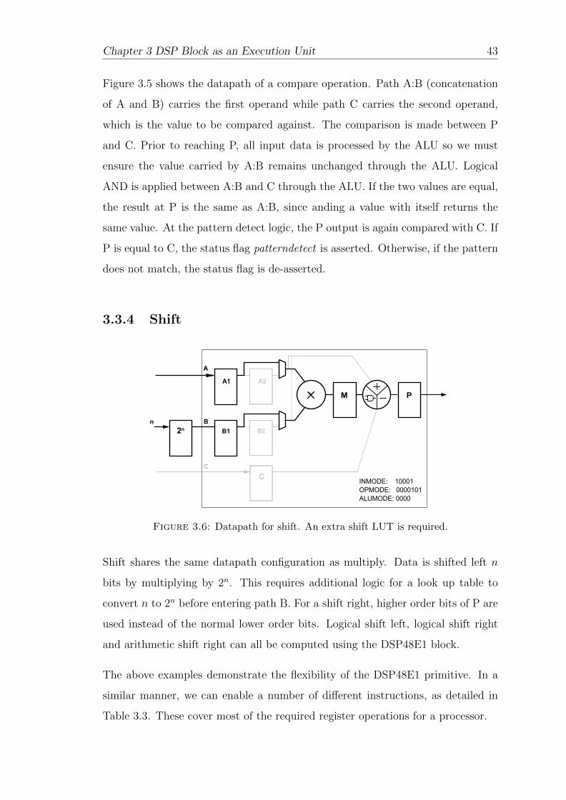
Chapter 3 DSP Block as an Execution Unit 43
Figure 3.5 shows the datapath of a compare operation. Path A:B (concatenation
of A and B) carries the first operand while path C carries the second operand,
which is the value to be compared against. The comparison is made between P
and C. Prior to reaching P, all input data is processed by the ALU so we must
ensure the value carried by A:B remains unchanged through the ALU. Logical
AND is applied between A:B and C through the ALU. If the two values are equal,
the result at P is the same as A:B, since anding a value with itself returns the
same value. At the pattern detect logic, the P output is again compared with C. If
P is equal to C, the status flag patterndetect is asserted. Otherwise, if the pattern
does not match, the status flag is de-asserted.
3.3.4 Shift
A1
B1
M P
2nn
A
B
INMODE: 10001OPMODE: 0000101ALUMODE: 0000
Figure 3.6: Datapath for shift. An extra shift LUT is required.
Shift shares the same datapath configuration as multiply. Data is shifted left n
bits by multiplying by 2n. This requires additional logic for a look up table to
convert n to 2n before entering path B. For a shift right, higher order bits of P are
used instead of the normal lower order bits. Logical shift left, logical shift right
and arithmetic shift right can all be computed using the DSP48E1 block.
The above examples demonstrate the flexibility of the DSP48E1 primitive. In a
similar manner, we can enable a number of different instructions, as detailed in
Table 3.3. These cover most of the required register operations for a processor.

Chapter 3 DSP Block as an Execution Unit 44
Table 3.3: Operations supported by the DSP48E1.
Operation INMODE OPMODE ALUMODE PathDSP Sub-stage
1 2 3
mul 10001 0000101 0000 mult A1, B1 M P
add 00000 0110011 0000 non-mult A1, B1, C0 A2, B2, C P
sub 00000 0110011 0011 non-mult A1, B1, C0 A2, B2, C P
and 00000 0110011 1100 non-mult A1, B1, C0 A2, B2, C P
xor 00000 0110011 0100 non-mult A1, B1, C0 A2, B2, C P
xnr 00000 0110011 0101 non-mult A1, B1, C0 A2, B2, C P
or 00000 0111011 1100 non-mult A1, B1, C0 A2, B2, C P
nor 00000 0110011 1110 non-mult A1, B1, C0 A2, B2, C P
not 00000 0110011 1101 non-mult A1, B1, C0 A2, B2, C P
nand 00000 0110011 1100 non-mult A1, B1, C0 A2, B2, C P
mul-add 10001 0110101 0000 both A1, B1, C0 M, C P
mul-sub 10001 0110101 0001 both A1, B1, C0 M, C P
mul-acc 10001 1000101 0000 both A1, B1, C0 M, P P
3.4 Balancing the DSP Pipelines
When switching operations, particularly between multiplication and non-multiplication
paths, pipeline depths are balanced to ensure correct computation. While pipelin-
ing the DSP block allows overlapping of operations during execution to improve
throughput, structural hazard can occur when two operations are trying to gain
access to the same functional unit simultaneously. To prevent this resource con-
flict, we designate a fixed pipeline depth for all DSP operations.
Table 3.4: Parameter attributes for pipelining the DSP48E1 datapaths.
Attribute Register
DSP PipelineStage
1 2 3
ADREG AD 0 0 0
AREG A 0 1 2
BREG B 0 1 2
CREG C 0 1 1
DREG D 0 0 0
MREG M 0 0 1
PREG P 1 1 1

Chapter 3 DSP Block as an Execution Unit 45
Table 3.4 shows the static parameter attributes responsible for pipelining of the
DSP datapaths. They determine the number of registers instantiated in the input
paths (A, B, C, D) and between the functional units (M, P). Column three shows
the correct values of each parameter for successful switching on a DSP block
pipelined at stages 1–3. Combinations other than those in Table 3.4 are supported,
but do not allow equal multiplier and non-multiplier depths. A non-pipelined DSP
block is possible, without any pipeline registers enabled.
A1
B1
M PCEA1
CEB1
CEM CEP
1 2 3
(a)
A1
B1
A2
B2
P
C0 C
CEA2
CEB2
CEC
CEA1
CEB1
CEP
1 2 3
(b)
Figure 3.7: Switching between multipy and add/subtract/logical path. Pathsare pipelined equally at 3 stages.
Figure 3.7 shows the pipelining of a multiplier path and an add/subtract/logical
path based on Table 3.4 set of parameter combination at three stages. Two reg-
isters are enabled at paths A and B: A1, A2 and B1, B2. In 3.7(a), registers A2
and B2 are bypassed. Multiplication is performed at the second stage, followed

Chapter 3 DSP Block as an Execution Unit 46
clock
multiply 5× 2 Stage 1 Stage 2 Stage 3
or 3 ∨ 3 Stage 1 Stage 2 Stage 3
output P 10 3
multiply 5× 2 Stage 1 Stage 2 Hazard
or 3 ∨ 3 Stage 1 Hazard
output P 3
Figure 3.8: Waveforms showing structural hazard of unbalanced pipelinedepths
by an ALU operation at the third stage. In 3.7(b), the multiplier is bypassed
and registers A2 and B2 are enabled in place of the bypassed register M. ALU
operation is performed at the third stage.
It is paramount to keep the ALU at the third stage for both type of operations. If
registers A2 and B2 are not enabled for non-multiplication operations, the pipeline
depth is shortened to 2 stages with the ALU executing in the second stage. When
an ALU is needed sooner due to shortened depth, resource conflict happens be-
tween the current operation and a preceding 3-stage multiply operation. Figure 3.8
shows the waveform of a balanced 3-stage multiply and non-multiply or operation,
followed a 3-stage multiply and 2-stage or. If the pipeline depths are unbalanced,
the output for both multiply and or operations are erroneous,
3.5 Iterative Computation on the DSP Block
In this section, we present two approaches to performing mathematical computa-
tions using the DSP block: the first approach takes advantage of its large number
of availability on the FPGA, while the second of its dynamic programmability. We
select a Chebysev polynomial as our case study, and the recursive relation of the
polynomial is given as:
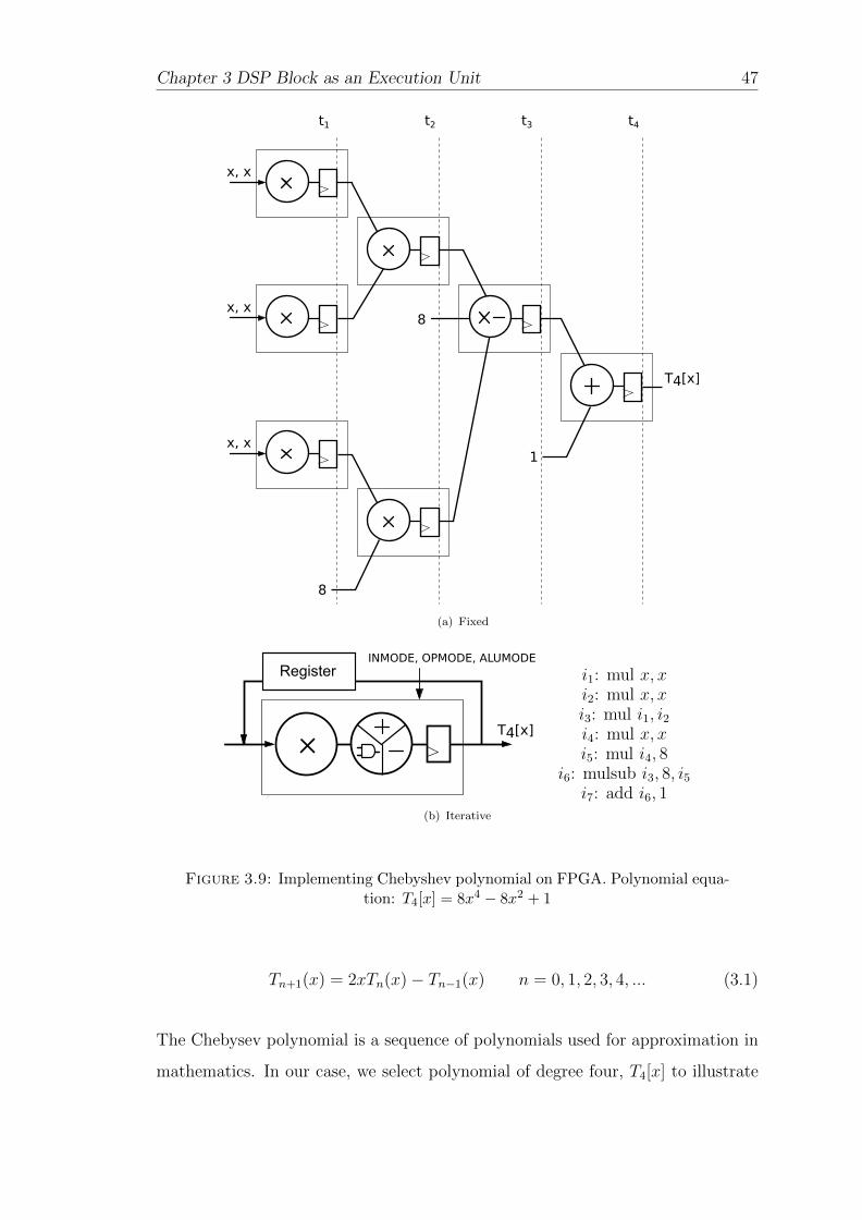
Chapter 3 DSP Block as an Execution Unit 47
x, x
x, x
x, x
8
8
T4[x]
1
t1 t2 t3 t4
(a) Fixed
RegisterINMODE, OPMODE, ALUMODE
T4[x]
i1: mul x,xi2: mul x,xi3: mul i1, i2i4: mul x,xi5: mul i4, 8
i6: mulsub i3, 8, i5i7: add i6, 1
(b) Iterative
Figure 3.9: Implementing Chebyshev polynomial on FPGA. Polynomial equa-tion: T4[x] = 8x4 − 8x2 + 1
Tn+1(x) = 2xTn(x)− Tn−1(x) n = 0, 1, 2, 3, 4, ... (3.1)
The Chebysev polynomial is a sequence of polynomials used for approximation in
mathematics. In our case, we select polynomial of degree four, T4[x] to illustrate

Chapter 3 DSP Block as an Execution Unit 48
Table 3.5: Comparing fixed and iterative Chebyshev polynomial implementa-tion.
Fixed Iterative
# DSP Blocks 7 1
Latency 4 7
our point. The polynomial is given as T4[x] = 8x4 − 8x2 + 1. This polynomial
degree is comprehensive enough to contain several different mathematical opera-
tions that are supported by the DSP block. To compute this equation, the DSP
blocks are constructed as shown in Figure 3.9(a). For operations that can be in-
dependently executed, they are constructed in parallel (i.e. multiply operations
at t1 and t2). The datapath is fixed and it reflects the order the mathematical
operations are performed. Each DSP block is configured to perform one mathe-
matical operation (multiply/add/multiply-subtract), and the values of INMODE,
OPMODE and ALUMODE are fixed throughout runtime. Multiply followed by
subtract operations are supported in the DSP, and these two operations are merged
and executed together in the same stage. For brevity, we pipeline the DSP block
at one-stage to simplify analysis. In this approach, the output of T4[x] is available
after 4 clock cyles, assuming a simple as-soon-as-possible (ASAP) scheduling. In
total, 7 DSP blocks are used to construct this computational circuit.
Figure 3.9(b) shows an alternate time-multiplexed, iterative approach to comput-
ing the Chebysev polynomial. We use a single DSP block for all the mathemati-
cal operations, also pipelined at one-stage latency for uniformity. In iteration i1
– i5, the DSP block performs multiply operation, then switches dynamically to
multiply-subtract at i6 and finally performs add at i7. In an iterative approach,
we need additional supporting hardware to store intermediate results and manage
the iteration sequence. In cases where the result of an iteration is not used im-
mediately, the value is placed temporarily in storage element known as a register
file. The control unit issues the correct control signals for every iteration, and also
supplies the correct inputs. One iteration takes one clock cycle, and the overall
latency for iterative computation is 7 clock cycles.

Chapter 3 DSP Block as an Execution Unit 49
Comparing these two approaches, a fixed datapath is faster, performing compu-
tation in fewer clock cycles. This design allows multiple independent operations
to execute concurrently. However, the operation of a DSP block is confined to
a single, fixed configuration, hence limiting the utilization of DSP in terms of
functionality. When configured in a iterative manner, we can perform up to three
operations per DSP block – or as many supported operations as possible, depend-
ing on the application. Furthermore, the iterative method is more flexible, as we
can reuse the circuit to execute different degrees of the Chebysev polynomial, by
changing the state machine control that manages the transition between iterations.
Additional hardware for control and storage may increase logic consumption, but
at the same time we save 7 DSP blocks, for use in other computational circuits.
Although there are different optimization opportunities for both the fixed and
iterative designs, we ignore these in the above example to simplify explanation.
This example is given purely to illustrate the difference between these two design
approaches. If we perform optimizations such as resource sharing, we could poten-
tially obtain a lower latency and DSP consumption for both (3 DSP blocks with
3 clock cycle latency).
3.6 Summary
In this chapter, we introduced the DSP48E1 and discussed its flexibility in support-
ing different arithmetic operations. The datapath can be easily manipulated to
switch between multiplication and non-multiplication operations during runtime.
We can configure the multiplier and ALU functionality, and balance the pipelines
to ensure correct computation through dynamic control signals and static param-
eter attributes. Lastly, we presented two approaches of performing mathematical
computations using the DSP block. In our case study, the iterative approach is
a viable alternative to a hardwired, fixed datapath. Comparatively, iterative also
minimizes DSP blocks usage but at the cost of 1.7× higher latency.

Chapter 4
iDEA: A DSP-based Processor
4.1 Introduction
In this chapter, we introduce iDEA: a 10-cycle, 32-bit soft processor that uses
a Xilinx DSP48E1 primitive as its execution unit. We first give an overview of
the processor architecture and the functional modules that make up the whole
processor. We discuss effective utilization of the DSP and BRAM primitives; as
execution unit, and instruction and data memory respectively. We show how to
use the irregular input widths of the DSP block with uniform 32-bit data. Finally,
we analyze the area, frequency and runtime of iDEA against the Xilinx Microblaze.
We also describe tools and benchmarks used for instruction count analysis.
The work presented in this chapter has been published in:
• H. Y. Cheah, F. Brosser, S. A. Fahmy, and D. L. Maskell, ”The iDEA
DSP Block Based Soft Processor for FPGAs”, in ACM Transactions on
Reconfigurable Technology and Systems (TRETS), vol. 7, no. 3, Article 19,
August 2014 [18].
• H. Y. Cheah, S. A. Fahmy, and D. L. Maskell, ”iDEA: A DSP Block Based
FPGA Soft Processor”, in Proceedings of the International Conference on
50

Chapter 4 iDEA: A DSP-based Processor 51
Field Programmable Technology (FPT), Seoul, Korea, December 2012, pp.
151–158 [19].
4.2 Processor Architecture
4.2.1 Overview
Recall that our key research question is to design an FPGA-optimized soft proces-
sor to be used as an alternative to an otherwise laborious and complex hardware
design. Although modern FPGAs offer high performance heterogeneous resources,
many soft processors suffer from not being fundamentally built around the FPGA
architecture. Most optimization aspects of embedded blocks are not utilized fully,
often deferring to the default options. Thus, to achieve our goal of designing a
fast, efficient soft processor architecture that fits closely to the low-level FPGA
target architecture, we are motivated to build a design from the ground up using
the FPGA hard primitives as the building blocks of major processor components.
The efficiency of a processor is largely determined by its instruction set architec-
ture [122]. For that reason, we chose a load-store RISC architecture for iDEA
based on its uniform instruction set. The RISC instruction set [123] consists of
small, highly optimized instructions designed to be executed efficiently regardless
of computation type. It has generous amount of registers to store intermediate
values between computations, which limits interactions with high latency memory.
Integer ALU operations and memory access operations are separated into differ-
ent class of instructions to maintain a simple decoding logic. A RISC compiler
is shown to produce more efficient code [124] because of the small number of in-
structions and efficient usage of registers. Scheduling of instructions is performed
statically in the compiler, instead of hardware. As the instruction set is simpler,
the processor has a straightforward decode logic and microarchitectural design.

Chapter 4 iDEA: A DSP-based Processor 52
Pipelining plays a significant role is the design of a RISC architecture. The pipeline
structure of a typical 5-cycle RISC is shown in Figure 4.1. With pipelining, dif-
ferent operations of an instruction can be separated into different stages: instruc-
tion fetch (IF), instruction decode (ID), instruction execute (EX), memory access
(MEM) and write-back (WB). During IF, instructions are retrieved sequentially
from the instruction memory. In the next cycle during ID, the fetched instruction
is decoded and appropriate values are assigned to the control signals. In the same
ID cycle, operands are fetched from the registers for execution. In EX, the ALU
performs arithmetic or logical operation on the operands. Alternately, the ALU
can be used to compute the effective address for memory access. In the case of
data memory store, data is stored in the MEM stage after EX. In the WB stage,
result from integer ALU operations or data memory read is stored back to the
register file.
IM Reg DM Reg
IF ID EX MEM WB
Figure 4.1: A RISC 5-cycle pipeline structure [1].
In the following sections, we present how the major components of iDEA are
constructed using FPGA primitives. Major functional units on the RISC pipeline
structure is shown in Figure 4.1. The units include instruction memory (IM),
register file (Reg), arithmetic logic unit (ALU) and data memory (DM).
4.2.2 Instruction and Data Memory
Instruction and data memory in iDEA are built using block RAMs (BRAMs).
They are synthesized into two separate RAMB36E1 primitives, with separate

Chapter 4 iDEA: A DSP-based Processor 53
memory spaces. The default BRAM synchronous read and write operations re-
quire only 1 clock cycle and the user has the option to enable an internal output
register to improve the clock-to-output timing of the read path. The internal out-
put register is located inside the BRAM primitive and if enabled, improves the
timing by 2.7× at the cost of an extra clock cycle of latency. Adding another
register in the logic fabric to register the output of the BRAM further improves
timing. We enable both the internal output register and logic output register for
the Instruction and Data Memory. The resulting latency of BRAM memory access
is 3 clock cycles.
Table 4.1: Maximum frequency of instruction and data memory in Virtex-6speed grade -2.
DescriptionMaximum Freq. (MHz)
Latency 2 Latency 3
CORE Generator 372 539
Inference (Read First Mode) 475 475
Inference (Write First Mode) 506 534
Inference (No Change Mode) 506 534
BRAM Virtex-6 Data Sheet 540
The way BRAMs are instantiated can affect their achievable frequency. Accord-
ing to the Virtex-6 FPGA Data Sheet [125], the highest frequency achievable by
a RAMB36E1/RAMB18E1 is 540 MHz. In Table 4.1, we show the frequencies we
were able to achieve for different design approach and register stages. At a latency
of two, a 512×32-bit memory, created using CORE Generator reaches a frequency
of only 372 MHz. CORE Generator is suitable for creating large memory struc-
tures, with more complex logic for address decoding, output muxing and other
additional features, but seems to be worse for small memory sizes.
Another method of instantiating block RAMs is through inference by the synthesis
tool. Memory is described behaviourally and the synthesis tool automatically
infers the required primitive. The resulting frequency of an inferred 512×32-
bit memory with a latency of two cycles, is 506 MHz. In order to achieve this

Chapter 4 iDEA: A DSP-based Processor 54
frequency, the memory must be described to infer No Change mode instead of
Read First or Write First. In more complex primitives like the DSP48E1, direct
instantiation is desirable as it provides full control of the features.
4.2.3 Register File
The register file makes use of the Xilinx LUT-based RAM32M primitive. This is
an efficient quad-port (3 read, 1 read/write) memory primitive that is implemented
using LUTs. The four ports are required to support two operand reads and one
write in each clock cycle. Block RAMs only provide two ports and are much larger
than required. To implement a 32×32-bit register file, 16 2-bit wide RAM23M
primitives are combined. Manual instantiation ensures only the required logic is
used. The RAM32M is an optimized collection of LUT resources, and a 32×32
register file built using 16 RAM32Ms consumes 64 LUTs, while relying on synthesis
inference resulted in usage of 128 LUTs.
Using a Block RAM for the register file may be beneficial as it would offer a
significantly higher register count. However, this would require a custom design
to facilitate the quad-port interface. In replication, an extra BRAM is needed
to support each additional read port, while the number of write ports remains
unchanged. If banking is used, data is divided across multiple memories, but each
read/write port can only access its own memory section. Similar to replication,
banking requires 2 BRAMs for a 3-read, 1-write register file.
Creating multi-ported memories for an arbitrary number of ports out of BRAMs is
possible, but entails both an area and speed overhead. In [98], an implementation
using Altera M9K BRAMs for a 2-write, 4-read multi-ported memory achieves
a clock frequency of 361 MHz, a 52.3% drop in frequency against a bare M9K
primitive. Hence, since we are targeting a design that is as close to the silicon
capabilities as possible, with as small an area as possible, we do not use BRAMs for
the register file, though this would be an option for more advanced architectures.
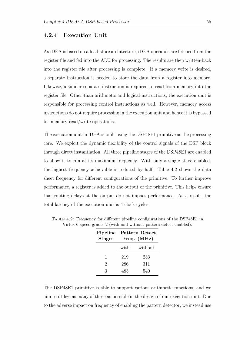
Chapter 4 iDEA: A DSP-based Processor 55
4.2.4 Execution Unit
As iDEA is based on a load-store architecture, iDEA operands are fetched from the
register file and fed into the ALU for processing. The results are then written-back
into the register file after processing is complete. If a memory write is desired,
a separate instruction is needed to store the data from a register into memory.
Likewise, a similar separate instruction is required to read from memory into the
register file. Other than arithmetic and logical instructions, the execution unit is
responsible for processing control instructions as well. However, memory access
instructions do not require processing in the execution unit and hence it is bypassed
for memory read/write operations.
The execution unit in iDEA is built using the DSP48E1 primitive as the processing
core. We exploit the dynamic flexibility of the control signals of the DSP block
through direct instantiation. All three pipeline stages of the DSP48E1 are enabled
to allow it to run at its maximum frequency. With only a single stage enabled,
the highest frequency achievable is reduced by half. Table 4.2 shows the data
sheet frequency for different configurations of the primitive. To further improve
performance, a register is added to the output of the primitive. This helps ensure
that routing delays at the output do not impact performance. As a result, the
total latency of the execution unit is 4 clock cycles.
Table 4.2: Frequency for different pipeline configurations of the DSP48E1 inVirtex-6 speed grade -2 (with and without pattern detect enabled).
PipelineStages
Pattern DetectFreq. (MHz)
with without
1 219 233
2 286 311
3 483 540
The DSP48E1 primitive is able to support various arithmetic functions, and we
aim to utilize as many of these as possible in the design of our execution unit. Due
to the adverse impact on frequency of enabling the pattern detector, we instead use

Chapter 4 iDEA: A DSP-based Processor 56
subtraction with a subsequent comparison implemented in LUTs for that purpose.
This also allows us to test for greater than and less than, in addition to equality.
DSP48E1 features that are relevant to iDEA functionality are:
• 25×18-bit multiplier
• 48-bit Arithmetic and Logic Unit (ALU) with add/subtract and bitwise logic
operations
• Ports A and B as separate inputs to the multiplier and concatenated input
to the ALU
• Port C as input to the ALU
• INMODE dynamic control signal for balanced pipelining when switching
between multiply and non-multiply operations
• OPMODE dynamic control signal for selecting operating modes
• ALUMODE dynamic control signal for selecting ALU modes
• optional input, pipeline, and output registers
Incorporating the D input and pre-adder would make the instruction format more
complex, likely requiring it to be widened, and would also require a more complex
register file design to support 4 simultaneous reads. Preliminary compiler analysis
on a set of complex benchmarks has shown that patterns of add-multiply-add/sub
instructions are very rare. Since we do not have access to intermediate stages of
the pipeline within the DSP block, we can only create a merged instruction when
three suitable operations are cascaded with no external dependencies. Hence, the
benefits of incorporating the D input and pre-adder into iDEA are far outweighed
by the resulting cost, and so we disable them.

Chapter 4 iDEA: A DSP-based Processor 57
4.2.5 Other Functional Units
All other functional units of the iDEA processor are implemented in LUTs. These
include the program counter, branch logic, control unit, input map and an adder
for memory address calculation. All the modules are combinational circuits except
for the program counter which is synchronous. These modules occupy minimal
LUT and register resources as the bulk of processor functionality is inside the
DSP48E1, which has a significant area and power advantage over a LUT-based
implementation of the equivalent functions.
4.2.6 Overall Architecture
InstructionMemory
RAMB36E1
Control Unit Register
FileRAM32M
Addr.Gen.
Input Map Execution Unit
DSP48E1
Data MemoryRAMB36E1
PC
Processor pipeline
Instruction Fetch Instruction Decode Instruction Execute
Internal pipeline
Branch
Figure 4.2: iDEA processor block diagram.
Using the primitives described in Section 4.2.2 – 4.2.4 as the major building blocks,
we construct a 32-bit, scalar load-store processor capable of executing a compre-
hensive range of general machine instructions called iDEA (DSP Extension Archi-
tecture). Only a single DSP48E1 is used for iDEA, with much of the processing for
arithmetic, logical operations and program control done within it. Apart from the
DSP48E1 for execution, other primitives are used for memory units: RAM32M
for the register file and RAMB36E1 for instruction and data memory. The overall

Chapter 4 iDEA: A DSP-based Processor 58
architecture is shown in Figure 4.2. Dark vertical bars represent processor stage
pipelines while light bars represent internal stage pipelines.
The processor functional units are split into the processor pipeline stages: instruc-
tion fetch (IF), instruction decode (ID) and instruction execute (EX), separated by
dark vertical bars as shown in Figure 4.2. Further internal pipelines (light vertical
bars) are enabled for stages that contain hard primitives. Although the ID stage
consists entirely of LUTs-implemented logic, we add an internal pipeline to im-
prove the propagation delay of this logic-congested stage. Memory access (MEM)
is located in the same stage as EX and the BRAM is pipelined at equal depth
as the DSP block. Since memory access instructions are separate from arithmetic
instructions, placing MEM and EX in the same stage does not affect functionality
of the processor. Conversely, a MEM stage before EX adds to a higher overall
pipeline depth (up to 3 extra stages).
The ID stage contains modules that perform auxiliary tasks such as generating
control signals, performing memory address calculations and mapping the right
operands to the DSP inputs. The control unit generates appropriate control sig-
nals for EX, WB and IF (branching select signals) based on the opcode of each
instruction. As iDEA’s pipeline structure does not allow the ALU to be used
for memory address calculations, we design an address generator to compute the
effective address instead. Lastly, the input map module assigns the operands
retrieved from the register file to the correct input ports, depending on the arith-
metic or logical operations. In-depth discussion on input mapping is presented in
Section 4.3.1.
4.3 Instruction Set Format and Design
The iDEA processor is designed to execute three types of instructions: data pro-
cessing, data transfer and program control. Instructions for these operations are
fixed at 32 bits, which fits comfortably into RAMB36E1 configuration as used for
the instruction memory. A subset of the iDEA instruction set is listed in Table A.1.

Chapter 4 iDEA: A DSP-based Processor 59
Though not as extensive as more advanced commercial processors, it is sufficient
to illustrate the functionality of iDEA as a general purpose processor. A uniform
32-bit instruction width is used. Unlike a typical execution unit that processes
only 2 input operands, our execution unit is capable of processing up to 3 input
operands and the instruction format is designed to cater for a third operand field
to reflect the extra processing capability as detailed in Table A.1.
Table 4.3: iDEA instruction set.
Instruction Assembly Operation
Arithmetic/ Logical
nop nop none
add add rd, ra, rb rd[31:0] = ra[31:0] + rb[31:0]
add rd, ra, #imm rd[31:0] = ra[31:0] + {16{#imm[15]},#imm[15:0]}sub sub rd, ra, rb rd[31:0] = ra[31:0] − rb[31:0]
sub rd, ra, #imm rd[31:0] = ra[31:0] − {16{#imm[15]},#imm[15:0]}mul mul rd, rb, rc rd[31:0] = rb[15:0] × rc[15:0]
mac mac rd, rb, rc, rp rd[31:0] = rb[15:0] × rc[15:0] + rp[31:0]
madd madd rd, ra, rb, rc rd[31:0] = ra[31:0] + (rb[15:0] × rc[15:0])
msub msub rd, ra, rb, rc rd[31:0] = ra[31:0] − (rb[15:0] × rc[15:0])
and and rd, ra, rb rd[31:0] = ra[31:0] and rb[31:0]
xor xor rd, ra, rb rd[31:0] = ra[31:0] xor rb[31:0]
or or rd, ra, rb rd[31:0] = ra[31:0] or rb[31:0]
nor nor rd, ra, rb rd[31:0] = ra[31:0] nor rb[31:0]
Data Transfer
lui lui rd, #imm rd[31:16] = {#imm[15:0], 16{0}}lw lw rd, [ra, rb] rd[31:0] = mem[ra[31:0] + rb[31:0]]
lw rd, [ra, #imm] rd[31:0] = mem[ra[31:0] + {16{#imm[15]}, #imm[15:0]}sw sw rd, [ra, rb] mem[ra[31:0] + rb[31:0]] = rd[31:0]
sw rd, [ra, #imm] mem[ra[31:0] + {16{#imm[15]}, #imm[15:0]} = rd[31:0]
Program Control
slt slt rd, ra, rb rd = 1 if ra[31:0] < rb[31:0]
slt rd, ra, #imm rd = 1 if ra[31:0] < {16{#imm[15]},#imm[15:0]}j j #target pc = #target
b{cond}* bcond ra, rb, #target (ra condition rb) pc = #target
*{cond} eq, gez, gtz, lez, ltz, bne
4.3.1 Input Mapping
Operands for processing are stored in the register file and the locations are ad-
dressed using the Ra, Rb, Rc and #imm fields in the instruction code. The width of
operands is 32 bits and immediate operands of lesser width are sign-extended to 32
bits. The input ports of the DSP48E1 have widths of 30 bits, 18 bits and 48 bits

Chapter 4 iDEA: A DSP-based Processor 60
Table 4.4: Port mapping for different arithmetic functions.
Assembly Operation Port A (30b) Port B (18b) Port C (48b)
add Rd, Ra, Rb C +A:B 16{Rb[31]}, Rb[31:18] Rb[17:0] 16{Ra[31]}, Ra[31:0]
add Rd, Ra, #imm C +A:B 30{1’b0} 2{imm[15]}, imm[15:0] 16{Ra[31]}, Ra[31:0]
sub Rd, Ra, Rb C −A:B 16{Rb[31]}, Rb[31:18] Rb[17:0] 16{Ra[31]}, Ra[31:0]
mul Rd, Rb, Rc C +A×B 15{Rb[15]}, Rb[15:0] 2{Rc[15]}, Rc[15:0] 48{1’b0}madd Rd, Ra, Rb, Rc C +A×B 15{Rb[15]}, Rb[15:0] 2{Rb[15]}, Rc[15:0] 16{Ra[31]}, Ra[31:0]
movl Rd, #imm C +A×B 30{1’b0} 18{1’b0} 32{1’b0}, imm[15:0]
for ports A, B and C respectively (Refer Figure 3.1); these widths are distinct and
not byte-multiples. To process 32-bit operands, data must be correctly applied to
these inputs.
The execution unit is designed to take two new 32-bit operands, addressed by Ra
and Rb, in each clock cycle. In the case of 2-operation, 3-operand instructions, a
third 32-bit operand, addressed by Rc is also used. Mapping a 32-bit operand to
the DSP48E1 input ports requires it to be split across corresponding input ports,
particularly for ports A and B, which are concatenated for ALU functions (A:B).
The data flow through the DSP48E1 can be represented as follows:
P = C + A : B (4.1)
and
P = C + A×B (4.2)
where P is the output port of DSP48E1. The “+” operation is performed by the
DSP48E1 ALU and can include add, subtract and logical functions. Port D is
excluded from the equation as it is disabled.
Equation 4.1 shows the flow for a 2-operand, single operation instruction. The
first operand, Ra, is mapped and sign-extended to the 48-bit port C. The second
32-bit operand, Rb, must be split across ports A and B; the least significant 18 bits
are assigned to port B and the most significant 14 bits sign extended to port A.
This is valid for operations that do not require a multiplier. Equation 4.2 shows a
3-operand, 2-operation instruction. Ra is mapped to port C, while Rb is assigned
to port A, and Rc to port B. The width of Rb and Rc is limited to 16 bits for

Chapter 4 iDEA: A DSP-based Processor 61
A1
B1
A2
B2
M P
= patterndetect
C
P
30
18
48
48
18
48
48
25
INMODE OPMODE ALUMODEA:B
RegisterFile
ControlUnit
OPCODE RA RBRD 0 0 0 0
Ra
Rb Op2
Op1
Op1[31:0]
Op1[17:0]
Op1[31:18]
Execution Unit
(a)
A1
B1
A2
B2
M P
= patterndetect
C
P
30
18
48
48
18
48
48
25
INMODE OPMODE ALUMODEA:B
RegisterFile
ControlUnit
OPCODE RA RBRD 0
C0
RC
Ra
Rb Op2
Op1
Op3[15:0]
Op2[15:0]
Op1[31:0]
RcOp3
Execution Unit
(b)
Figure 4.3: (a) 2-operand (b) 3-operand input map.
multiplication. In the case of multiply only, port C is set to zero. In multiply-add,
multiply-sub or multiply-acc, port C carries the third operand.
The DSP48E1 can be dynamically switched between operations defined by Equa-
tions 4.1 and 4.2 through the INMODE, OPMODE and ALUMODE control sig-
nals. Table 4.4 illustrates the port mappings for some common instructions while
Chapter 4 iDEA: A DSP-based Processor 62
Figure 4.3(a) and Figure 4.3(b) show how the fields in the instruction are mapped
to an operation in the DSP48E1 execution unit. As mentioned in Section 4.2.6, the
computation of base and offset addresses for data memory access is not performed
by the execution unit. Instead, we use a separate unit called memory address
adder and the DSP48E1 is bypassed for memory access instructions. This allows
memory instructions to complete in the same latency.
4.3.2 DSP Output
Multiplication and shift can be performed directly in the DSP84E1, using the built-
in multiplier. With the ALU that follows the multiplier, two consecutive arithmetic
operations on the same set of data can be performed, including multiply-add
and multiply-accumulate. The DSP48E1 primitive produces an output of 48 bits
through port P, regardless of the type of arithmetic operation; the least significant
32 are written back to the register file.
It is important to note, that the DSP48E1 multiplier width is only 25×18 bits. To
fully implement a 32×32 multiplier, three DSP48E1 primitives can be cascaded
together, but this triples the resource requirement for the benefit of only a single
instruction. Hence, we restrict multiplication to 16×16 bits, producing a 32-bit
result, which still fits the iDEA specification. A wider multiplication than 16 bits
would not be beneficial, since the result would have to be truncated to fit the
32-bit data format. For operations that involve the multiplier, data inputs are
limited to 16 bits, while for other operations they are 32 bits. If a wide multiply
is required, it can be executed as a series of 16-bit multiplications. For floating
point operations, we can use the compiler to translate them into a series of steps
that can be executed using the DSP48E1 primitive, as per the method in [126],
similar to the soft float approach in many compilers.

Chapter 4 iDEA: A DSP-based Processor 63
4.4 Hardware Implementation
In this section, we analyze the area and performance of iDEA at different pipeline
depths, and provide an at-a-glance comparison with MicroBlaze [8], a 32-bit com-
mercial soft processor from Xilinx. We choose MicroBlaze as it is freely avail-
able and easily supported by the Xilinx development toolkit. In Section 4.6.2,
we benchmark a few general purpose applications to demonstrate the functional-
ity of iDEA. All implementation and testing is performed on the Xilinx Virtex-6
XC6VLX240T-2 device as present on the Xilinx ML605 development board.
4.4.1 Area and Frequency Results
Table 4.5 shows the post-place-and-route implementation results for iDEA and
MicroBlaze. For iDEA, the implementation is performed using Xilinx ISE 14.5
while MicroBlaze is implemented using Xilinx Platform Studio (XPS) 14.5. The
XPS is an extension of the ISE design suite specifically provided for the design
of MicroBlaze processor-based systems. Both implementations include memory
subsystems and the processor core. A total of 4KB is allocated for instruction and
data memory for each of the processors.
As the Xilinx DSP48E1 and RAMB36E1 primitives used in iDEA are highly
pipelinable, we study the effect of varying the number of primitive pipeline stages
from 1–3. This translates to an overall processor pipeline depth of 4–10 stages.
As expected, a deeper pipeline yields a higher clock frequency. From the mini-
mum pipeline depth of 4 to a maximum pipeline depth of 10, the clock frequency
increases by 2.5× at a cost of 2.3× more registers and 1.3× more LUTs. The in-
crease in LUTs is lesser than registers as processor functionality does not change
with increasing depth.
In order to quantify the benefit of using the DSP48E1 in the manner we have,
we coded the exact behaviour of the DSP-based execution unit and implemented
it in the logic fabric. Table 4.5 shows a LUT-based equivalent (pipeline depth of

Chapter 4 iDEA: A DSP-based Processor 64
Table 4.5: Frequency and Area for iDEA and MicroBlaze.
Pipeline DepthFreq.
(MHz)Registers LUTs DSP48E1
iDEA
4 182 237 280 1
5 266 371 281 1
6 270 370 283 1
7 311 315 306 1
8 355 479 336 1
9 405 613 365 1
10 453 542 362 1
10 LUTs-only 169 792 878 1
MicroBlaze
3 189 276 630 3
5 211 518 897 3
10) occupies 1.5× more registers and 2.4× more LUTs compared to a DSP-based
iDEA. In addition to slice logic, the tool still synthesized a DSP block for the
16×16 multiplication. The LUT-based equivalent achieved a clock frequency of
169 MHz, just 37% of iDEA’s frequency. This shows that our design that takes
advantage of the low level capabilities of the DSP block is highly efficient.
The MicroBlaze results are presented purely to give a sense of relative scale, and
we do not claim that iDEA can replace MicroBlaze in all scenarios. To make the
comparison fairer, we configure the smallest possible MicroBlaze while keeping
all the basic functionality necessary to run applications. Extra peripherals and
features that are not available in iDEA, such as cache, memory management, and
the debug module are disabled. The multiplier is enabled and set to the minimum
configurable width of 32 bits. Other hardware like the barrel shifter, floating
point unit, integer divider and pattern comparator are disabled. Accordingly,
the MicroBlaze compiler does not generate instructions that utilize these disabled
features.
MicroBlaze can be configured with two different pipeline depths, 3 stages for an

Chapter 4 iDEA: A DSP-based Processor 65
area-optimized version or 5 stages for a performance-optimized version. The 5-
stage MicroBlaze uses 88% more registers and 42% more LUTs. MicroBlaze in-
cludes some additional fixed features such as special purpose registers, instruction
buffer, and bus interface, which contribute to the higher logic count. These Mi-
croBlaze features are not optional and cannot be disabled. MicroBlaze also sup-
ports a wider multiplication width of 32×32, resulting in the use of 3 DSP48E1
blocks instead of one. A 3-stage area-optimized MicroBlaze occupies 49% fewer
registers and 74% more LUTs than a 10-stage iDEA. A reduced 4-stage version
of iDEA would be on par with the 3-stage MicroBlaze in terms of frequency and
registers, but still consumes 56% fewer LUTs.
To confirm the portability of iDEA, we also implemented the design on the Xilinx
Artix-7, Kintex-7, and Virtex-7 families. The resource consumption and maximum
operating frequency post-place-and-route, shown in Table 4.6, are mostly in line
with the Virtex-6 results, with the low-cost Artix-7 exhibiting reduced frequency.
These results may improve slightly as tools mature, as is generally the case for
new devices.
Table 4.6: 10-stage iDEA in Artix-7, Kintex-7 and Virtex-7.
Resource Virtex-6 Artix-7 Kintex-7 Virtex-7
Slice Registers 542 541 537 541
Slice LUTs 362 454 451 450
RAMB36E1 2 2 2 2
DSP48E1 1 1 1 1
Freq (MHz) 453 453 504 504
4.5 Software Toolchain
Having built iDEA, we would now like to evaluate its performance for executing
programs. It is important to state that iDEA is, by definition, a lean processor
for which performance was not the primary goal. Additionally, as of now, there is
no optimized compiler for iDEA, so the results presented in this section are aimed

Chapter 4 iDEA: A DSP-based Processor 66
primarily at proving functionality and giving a relative performance measure. Only
with a custom compiler can we extract maximum performance and enable the use
of iDEA’s unique extra capabilities.
iDEA We gather experimental results using an instruction set simulator writ-
ten for iDEA. The simulator is written in Python to model the functionality of
the iDEA processor. Using the simulator, we obtain performance metrics such
as instruction count and number of clock cycles, as well as ensuring logical and
functional correctness. We chose an existing MIPS I compiler that supports an
instruction set similar to that of iDEA. The benchmark programs are written in
C and compiled to elf32-bigmips assembly code using the mips-gcc toolset. The
instructions generated must be translated to equivalent iDEA instructions. The
simulator consists of an assembly code converter and a pipeline simulator. The
complete toolchain from C program to simulator is illustrated in Figure 4.4.
Standard CCompiler
AssemblyConverter
Simulator*.c
logs, statis-tics, mem-ory state
*.asm *.asm
Figure 4.4: Simulator and toolchain flow.
MicroBlaze The instruction count and clock cycle count for MicroBlaze are ob-
tained by testbench profiling using an HDL simulator, as the Xilinx Platform
Studio (XPS) 14.5 does not provide an instruction set simulator for MicroBlaze.
MicroBlaze simulator is available in earlier XPS versions, but is already made
obsolete in the version used in this work. The testbench and simulation files for
MicroBlaze are automatically generated by XPS. In the testbench, we added a
module that tracks the instruction count in every clock cycle. The tracker is
started at the beginning of a program and terminates once it is complete. With
every valid instruction issued, the instruction counter is incremented. The start
and end signals are obtained from the instruction opcode in the disassembly file.
The C code is compiled using the C compiler from the Xilinx Software Develop-
ment Kit 14.5 (SDK), mb-gcc into an .elf executable. This can be viewed as a
disassembly file. From this, we locate when a computation starts and ends and

Chapter 4 iDEA: A DSP-based Processor 67
the corresponding program counter address. Once the tracker module encounters
these addresses, it starts and stops the count tracking accordingly.
4.5.1 Assembly Converter
The assembly converter takes as its input an elf32-bigmips format assembly file,
the standard assembly code format produced by mips-elf-gcc. By setting the ap-
propriate flags, -c -g -O, the compiler bypasses the linker, instead giving only the
assembly code. This assembly code is converted to the format used by the iDEA
simulator, and then processed to prepare for execution in the simulator. These
preparations include expanding pseudo-instructions found in the assembly code,
performing instruction substitutions where necessary to fit the iDEA instruction
set, NOP insertion and classification of instruction types for collation of statis-
tics. The simulator’s data memory is pre-loaded with the data specified in the
elf32-bigmips assembly code. Because the iDEA architecture does not currently
implement hardware stalling or data forwarding, dependencies have to be resolved
in software. The code is checked for dependencies and no-operation instructions
(NOPs) are inserted where necessary to avoid data hazards.
4.5.2 iDEA Simulator
The simulator can be configured to model a variable number of pipeline stages and
different pipeline configurations. All iDEA instructions that are used in the bench-
marks are supported by the simulator. The simulator models the iDEA pipeline
stage by stage and the execution of the instructions as they pass between stages.
The register file, data memory and instruction memory are modelled individually
as separate modules. The statistics collected during each simulation run are cycle
count, NOP count, simulation run time and core cycle count.
We manually insert the start and end tags in the assembly source code to define
where the computational cores of the programs start and end, with the purpose

Chapter 4 iDEA: A DSP-based Processor 68
of eliminating initialization instructions from the final cycle count. The results
presented in Section 4.6.2 are the core cycle counts.
4.5.3 Benchmarks
Seven benchmarks, briefly presented below, are used to evaluate performance.
The benchmarks are written in standard C with an internal self-checking loop to
verify correctness and reduce simulator complexity. The applications are funda-
mental loops; they are kernels of larger algorithms and often the core computation
loops of more extensive, practical applications. For example sorting algorithms are
commonly found in networking applications; fir and median filters are found in
digital signal processing applications; crc in storage devices and matrix multipli-
cation in linear algebra. We do not restrict our benchmarks to a specific domain,
rather keeping the benchmark suite general purpose to demonstrate the range of
applications that iDEA can support.
• bubble – bubble sort on an array of 50 random integers
• crc – 8-bit CRC on a random 50 byte message
• fib – calculating the 50 first Fibonacci numbers
• fir – an FIR filter using 5 taps on an array of 50 integers
• median – a median filter with a window size of 5, on an array of 50 integers
• mmult – matrix multiplication of two 5×5 integer matrices
• qsort – quick-sort on an array of 50 random integers
These benchmarks are sufficient to demonstrate the complete toolchain of iDEA
including compiler, simulator, and processor. We evaluate the benchmarks at
compiler optimization levels of O0–O3 for both mips-gcc and mb-gcc. Optimization
levels determine the efficiency of compiled code in terms of speed and size. The -O0
has no optimization performed and is a straightforward translation from source

Chapter 4 iDEA: A DSP-based Processor 69
program to output, while -O3 performs full optimization. We use the default
options defined for the optimization levels, both for iDEA and MicroBlaze, without
enabling extra compiler options.
4.6 Execution Results
4.6.1 NOPs and Pipeline Depth
A crucial question to answer is how to balance the number of pipeline stages with
the frequency of operation. Enabling extra pipeline stages in FPGA primitives
allows us to maximize operating frequency as demonstrated in Section 4.4, how-
ever, we must also consider how this impacts processor performance as a whole,
and the resulting cost in executing code. Figure 4.5 shows the frequency and wall
clock times for the benchmarks we tested at optimization level of -O3. The fre-
quency plot is based on the iDEA pipeline depths of 4–10 as previously shown in
Table 4.5. It is clear that 10 pipeline stages provides the highest performance in
terms of operating frequency.
However, this comes at a cost: since iDEA is a simple processor with no data
forwarding, we must insert no-operation instructions (NOPs) to overcome data
hazard between dependent instructions. Number of NOPs for each corresponding
pipeline depth is shown in Table 4.7. With a longer pipeline, more NOPs are
needed, which may impact program runtime. In Figure 4.5, the execution time
shows an increase from depths of 5–9, due to the higher number of NOPs at these
pipeline depths. Higher number of NOPs contribute to the higher number of total
instruction count, which minimizes the benefits of high frequency. At pipeline
depth of 10, however, the increase in NOPs is limited, allowing the high frequency
gain to result in decreased execution runtime.

Chapter 4 iDEA: A DSP-based Processor 70
50
60
70
80
90
Tim
e(u
s)
4 5 6 7 8 9 10
200
300
400
500
Pipeline Depth
Fre
quen
cy(M
Hz)
FrequencyExecution Time
Figure 4.5: Frequency and geomean wall clock time at various pipeline depths.
Table 4.7: Number of NOPs inserted between dependent instructions.
PipelineDepth
IF ID EX WB #NOPsNOPs
Increase
4 1 1 1 1 2 –
5 1 2 1 1 3 1.5×6 2 2 1 1 3 1.0×7 3 1 2 1 4 1.33×8 2 2 3 1 5 1.25×9 2 3 3 1 6 1.2×10 3 2 4 1 6 1.0×
4.6.2 Execution Time
With a compiler, we generate instruction code for a 10-cycle iDEA for the bench-
marks at different optimization levels. Figure 4.6 shows the total execution time of
both processors for all seven test applications (bubble, fib, fir, median, mmult,
qsort and crc), at four different optimization levels (O0, O1, O2, O3). Overall,
iDEA has a higher execution time compared to 5-cycle MicroBlaze due to the in-
sertion of NOPs to handle data hazards. Figure 4.7 shows the relative execution
time of iDEA with MicroBlaze normalized to 1 for each optimization level. Of
all the benchmarks, CRC is the only application that has faster execution time
on iDEA than MicroBlaze; despite a higher number of clock cycles, the improved
frequency of iDEA results in a lower execution time.

Chapter 4 iDEA: A DSP-based Processor 71
bubble crc fib fir median mmult qsort0
50
100
150
200
702.
14
189.
47
27.9
4
121.
41
101.
31
90.5
172.
93
154.
14
69.5
3
11.3
6 35.4 44
.82
23.1
4
74.5
1
161.
76
65.7
4
11.0
6 31.1
6
40.2
8
19.0
6
56.5
9
161.
76
62.8
10.8
6
6.65
34.2
7
3.01
56.5
9
411.
64
189.
45
9.19
67.1
4
56.8
4
40.2
9
91.4
8
128.
95
108.
57
2.56
24.0
7
21.5
2
16.8
6 40.7
8
92.1
5
104.
33
2.55 18
.18
18.7
5
14.1
9
28.9
8
92.1
5
104.
19
2.33
0.48
20.7
6
0.74
28.9
8
Exec
uti
onT
ime
[µS
]
iDEA -O0 iDEA -O1 iDEA -O2 iDEA -O3Microblaze -O0 Microblaze -O1 Microblaze -O2 Microblaze -O3
Figure 4.6: Comparison of execution time of iDEA and MicroBlaze at maxi-mum pipeline-depth configuration.
MicroBlaze
bubble crc fib fir median mmult qsort0
1
2
3
4
5
1.71
1
3.04
1.81
1.78 2.
25
1.89
1.2
0.64
4.44
1.47
2.08
1.37 1.
83
1.76
0.63
4.34
1.71 2.
15
1.34
1.95
1.76
0.6
4.66
13.8
5
1.65
4.07
1.95
Rat
ioof
Exec
uti
onT
ime -O0
-O1-O2-O3
Figure 4.7: Execution time of iDEA relative to MicroBlaze.
In most benchmarks, the NOP instructions make up the vast majority of the total
instructions executed — between 69.0% and 86.5%. This can be partially traced
to the register allocation process in the compiler, which strictly assigns register
usage based on its function (e.g. return values are only stored in registers v0 and
v1), resulting in many NOPs being inserted to resolve dependencies. Currently,
the same registers are often re-used for consecutive instructions which creates
dependencies that have to be resolved by NOP insertion or stalling. Restrictions
on register allocation prevents efficient use of registers, where a specific set of
registers are used repeatedly while some reserved registers are not utilized at all.
Chapter 4 iDEA: A DSP-based Processor 72
The effect of register re-use is particularly evident in fib, fir and mmult. At
optimization level -O3, the loop is unrolled to a repeated sequence of add and store
instructions without any branching in between. While the absence of branching
reduces the branch penalty, the consecutive dependency between the instructions
demands that NOPs be inserted causing an increase in overall execution time.
In order to maintain the leanness of iDEA, we initially avoided the addition of data
forwarding or stalling. However, noting the significant number of NOPs required
to resolve dependencies, we later added a lean data forwarding technique by using
the feedback path of the DSP block in Chapter 6. Further discussions on effect of
pipeline depth and data hazards are also presented in the same chapter.
4.6.3 Multiply-Add Instructions
With the availability of two arithmetic sub-components in iDEA (or three in the
DSP48E1 if the pre-adder is enabled), we can explore the possible benefits of com-
posite instructions, by combining several operations into a single instruction. For
example, two consecutive instructions mul r3, r2, r1; add r5, r4, r3 have a
read after write (RAW) dependency and NOPs have to be inserted to allow the
result of the first instruction to be written back to the register file before execution
of the second. By combining these into a single instruction mul-add r5, r1, r2,
r4, two instructions can be executed as one, reducing the number of useful instruc-
tions required to perform the same operations, and also removing the necessity for
NOPs in between.
The three operand multiply-accumulate instruction maps well to the DSP48E1
block and is supported by the iDEA instruction set. To explore the potential
performance improvement when using composite instructions, we examine the
fir and mmult benchmarks after modifying the code to use the madd instruction.
Currently, this modification is done manually, as the compiler does not support this
instruction. We manually identify the pattern mult r3, r1, r2; add r4, r4,

Chapter 4 iDEA: A DSP-based Processor 73
r3 and change it to madd r4, r1, r2. A compiler could automatically identify
the multiply-accumulate pattern and make use of the instruction.
No composite
fir mmult0
0.5
1
1.5
0.94
0.96
0.82 0.860.
93
0.84
Rat
ioof
Exec
uti
onT
ime
-O0-O1-O2
Figure 4.8: Relative execution time of benchmarks using composite instruc-tions
Figure 4.8 shows the relative performance when using these composite instruc-
tions compared to the standard compiler output (normalized to 1). We see that
the use of composite instructions in a 10-stage iDEA pipeline can indeed pro-
vide a significant performance improvement. Benchmark fir at -O1 shows the
best execution time improvement, 18%, while the -O0 optimization level for both
benchmarks shows only slight improvements; 6% and 4% for fir and mmult re-
spectively. The benchmarks that are shown here use computation kernels that
are relatively small, making the loop overhead more significant than the compu-
tations themselves, thus limiting the potential for performance savings. For more
complex benchmarks, there is a greater potential for performance improvement
resulting from the use of composite instructions. Our preliminary analysis shows
that it is possible to extract opportunities for composite instructions in common
embedded benchmark programs, not just programs from a specific domain such as
DSP processing or media processing. A full analysis on the feasibility of composite
instructions is presented in the following Chapter 5.

Chapter 4 iDEA: A DSP-based Processor 74
4.7 Summary
In this chapter we presented iDEA, an instruction set-based soft processor for
FPGAs built with a DSP48E1 primitive as the execution core. We harness the
strengths of the DSP48E1 primitive by dynamically manipulating its functionality
to build a load-store processor. This makes the DSP48E1 usable beyond just signal
processing applications.
As iDEA is designed to occupy minimal area, the logic is kept as simple as possible.
By precluding more complex features such as branch prediction, we are able to
minimize control complexity. The processor has a basic, yet comprehensive enough
instruction set for general purpose applications. We have shown that iDEA runs
at about double the frequency of MicroBlaze, while occupying around half the
area. iDEA can be implemented across the latest generation of Xilinx FPGAs,
achieving comparable performance on all devices.
We presented a set of seven small benchmark programs and evaluated the per-
formance of iDEA by using translated MIPS compiled C code. We showed that
even without a customized compiler, iDEA can offer commendable performance,
though it suffers significantly from the need for NOP insertion to overcome data
hazards. We also evaluated the potential benefits of iDEA’s composite instruc-
tions, motivating a more thorough LLVM-based analysis in Chapter 5. A method
to reduce the number of idle NOPs in the form of a DSP-internal forwarding path
is presented in Chapter 6.

Chapter 5
Composite Instruction Support in
iDEA
5.1 Introduction
In Chapter 4, we saw that the deep pipeline of iDEA leads to a high number of idle
cycles being required between dependent instructions. Deep pipelining enables our
processor design to operate at close to maximum frequency of the DSP block, but
suffer from decreased performance due to long dependency chains in the instruction
stream. We also showed how the DSP block can support composite operations,
which reduce these idle cycles, thereby increasing performance. In this chapter,
we explore the idea of identifying and supporting application-specific composite
instructions, derived from the DSP block architecture. The DSP block internally
supports multi-operation sequences that naturally match instruction sequences in
many programs. We explore how instruction sequences from C source programs
can be mapped into DSP block sub-components: the pre-adder, multiplier and
ALU, to form composite instructions. These instructions, executed using a com-
bination of these components, avoids dependency issues between instructions by
capturing the inter-instruction data within the composite instruction itself. In this
chapter, we evaluate the opportunities for such instructions, and their benefits.
75

Chapter 5 Composite Instruction Support in iDEA 76
5.2 Potential of Composite Instruction
mult
add
mult y, a, badd d, y, c
madd d, a, b, c
a b
c
d
a b c
d
Figure 5.1: Mapping a two-node subgraph to DSP block. Pre-adder is notdepicted.
Composite instructions are multi-operation instructions that can be executed in
a single iteration through the processor datapath. This is possible because of
the multiple sub-components in the DSP block that enables the processing of
different arithmetic operations. The purpose of composite instruction is to reduce
instruction count, thereby increasing speedup by introducing new instructions that
execute multiple arithmetic operations. By introducing composite instructions, we
extend the instruction set of our base processor. Composite instructions are not
necessarily application-specific, and they can be used across application domains.
Figure 5.1 shows the process of mapping and fusing a composite instruction.
A composite instruction is selected through the analysis of the dependence graph
of a program’s intermediate representation. High-level code is first compiled into
an intermediate representation (IR), formed of basic blocks. We retrieve data
dependence information from the basic blocks and apply composite pattern iden-
tification on the dependence graph. Selecting the final set of composite instruc-
tions involves finding a solution that maximizes the number of non-overlapping,
two-node instructions of a dependence graph. The selected nodes for a composite
instruction must agree with the arithmetic functionality and order of the sub-
components in the DSP block. The order of the sub-components is: pre-adder,
multiplier, then ALU. The pre-adder and multiplier can be bypassed, but the ALU

Chapter 5 Composite Instruction Support in iDEA 77
is utilized in all arithmetic operations including multiply. For the multiply opera-
tion, the ALU input multiplexers select multiplier results and pass them directly
to the DSP block output, without performing any operations. Legal combinations
of composite instructions are discussed in Section 5.6.
5.3 Related Work
The work in this chapter bears similarities with custom instruction synthesis in
two ways: instruction set extension and instruction pattern analysis. We review
work related to these aspects.
Research on extending the instruction set (ISA) of a microprocessor by analyzing
the behaviour of its target application is well established in the context of exten-
sible processors [127–132]. The instruction set of an extensible processor is cus-
tomizable by adding extra functional units to the datapath of the base processor.
The goal is to increase performance by tuning the ISA to be application-specific,
while satisfying the demands of shorter time to market expected of embedded ap-
plications. Notable commercial extensible processors are Tensilica Xtensa [133],
STMicroelectronics Lx [134], Synopsys ARC [135] and the Altera Nios soft pro-
cessor family [7].
The custom functional unit in an extensible processor execute specially-defined
instructions, known as custom instructions. Custom instructions are chosen by
profiling an application to identify and select instruction patterns that are most
profitable to an application, subject to constraints. Although analysis of can-
didates for custom instructions is normally done in the intermediate represen-
tation [129, 130, 132], there are cases where the analysis is done in the program
execution trace [131,136]. Analysis in the execution trace widens the search space
to include inter-basic block opportunities. However, inter-basic block custom in-
structions are very sensitive to changes in program flow and the search space is
potentially exponential. Our analysis to identify instruction patterns is done in
IR and we limit the analysis to within the boundaries of basic blocks.

Chapter 5 Composite Instruction Support in iDEA 78
Various constraints can be imposed when determining custom instructions such as
number of operands, number of custom instructions, and area. There are various
methods proposed to find the optimal number of operands for a custom instruc-
tion, by imposing limits of 2-input, 1-output [128] to multiple-input, multiple-
output [127]. The optimal number of operands is identified to be 4-input, 3-
output [131]. Although the DSP block can support up to 4-inputs and 1-output,
the primary microarchitectural constraint on iDEA is the set of legal operations
supported by the DSP sub-components, rather than number of operands. The
number of implementable custom instructions in most extensible processors is re-
stricted due to limited length of the opcode field. Taking this constraint into
consideration, [129] developed an algorithm that searches for the maximum appli-
cation speedup with a limited number of custom instructions.
Although custom instructions targetted at FPGAs are rare [137–139], existing
analysis techniques and heuristics are applicable. Work in [137] applied a minimum-
area logic covering derived from existing instruction mapping algorithms. The
techniques introduced improve execution speed, by minimizing area cost. Tech-
niques to effectively map custom instructions into FPGAs were further explored
in [138, 139]. The algorithm estimates the utilization of LUTs prior to actual
synthesis and implementation for rapid selection of FPGA custom instructions.
The work in [127–132,136–139] all shows how extending the instruction set through
custom instructions can result in considerable performance gain. However, cus-
tom instructions are implemented as an additional functional unit outside of the
main ALU, incurring extra hardware cost. Custom instructions are application-
specific; an implemented custom instruction may be beneficial in an application,
but not yield any performance increase for another application. In this chapter,
we determine composite instructions for iDEA using the same analysis as for cus-
tom instructions; instruction identification followed by instruction selection. We
limit the our pattern identification to within the basic blocks, and the number of
operands to 3-input, 1-output, and we do not consider overlapping patterns. We

Chapter 5 Composite Instruction Support in iDEA 79
compile our application to a standard intermediate representation, perform iden-
tification on the dependence graph, and select our composite instructions using a
linear optimization algorithm.
5.4 Intermediate Representation
We use the LLVM Compiler Infrastructure [140] as our analysis tool to identify
data dependency opportunities in our benchmarks. LLVM is a development in-
frastructure enabling users to build a compiler, and numerous tools are available
to assist compiler designers to develop, optimize and debug a compiler software.
One of the reasons LLVM gained widespread following is due to its modular, clean
separation between front-end and back-end, which makes it capable of supporting
many source languages and target architectures. The front-end of the compiler
is responsible for accepting and interpreting the input source program, while the
back-end translates the functionality into a target machine language.
Front-endSource
OptimizationIR
Back-endIR Target
Figure 5.2: Compiler flow.
LLVM generates an intermediate representation (IR) that encodes the program
as a series of basic blocks containing instructions. The LLVM IR is a linear IR,
with 3-address code instructions. Linear IRs look very similar to assembly code,
where the sequence of instructions executes in the order of appearance. They are
compact and easily readable by humans, and 3-address instructions map well into
the structure of many processors. Optimizations can be applied to the IR in order
to improve the final machine code generated by the back-end. Often optimizations
are performed with two end goals in mind: to produce code that executes faster
or occupies smaller memory space.

Chapter 5 Composite Instruction Support in iDEA 80
Table 5.1: A 3-address LLVM IR. The basic block shows the sequence ofinstructions to achieve multiply-add: load into register, perform operation, store
back to memory.
; <label >:6 ; preds = %2
%7 = load i32* %a, align 4
%8 = load i32* %b, align 4
%9 = mul nsw i32 %7, %8
store i32 %9, i32* %c, align 4
%10 = load i32* %c, align 4
%11 = load i32* %d, align 4
%12 = add nsw i32 %10, %11
store i32 %12, i32* %e, align 4
br label %13
LLVM IR provides high-level information crucial for analysis and transformations
of a program, while avoiding low-level machine-specific constraints; and allows ex-
tensive optimization at all stages, through optimization of the IR. Transformation
requires changing and re-writing the information contained in the IR, like dead
code elimination or loop unrolling. Analysis passes that do not alter the IR are
also supported. We use analysis passes for our investigations.
In intermediate representation, information on the control flow of a program is
expressed in the form of a basic block. A basic block consists of instructions
that execute consecutively until a terminator instruction is reached i.e., branch
or function return. A basic block has only one entry point and exit point, and a
terminator instruction is an exit point. The relationship between basic blocks in a
function is modelled in a control flow graph while the relationship between instruc-
tions in a basic block is the dependence graph. The control flow and dependence
of a multiply-add function are illustrated in Figure 5.3.
The interaction between instruction nodes in a dependence graph is constructed
using the def-use chain [141]. The chain analyses the flow of a value from its
definition point, to its use point. The definition point is where the value is created,
and use point is where the value is used, or consumed. There must not be any re-
definitions of the value in-between these two points. A definition can have several

Chapter 5 Composite Instruction Support in iDEA 81
%0: ... br label %2
%2:
%3 = load i32* %i, align 4 %4 = load i32* %n, align 4 %5 = icmp slt i32 %3, %4 br i1 %5, label %6, label %16
T F
%6:
%7 = load i32* %a, align 4 %8 = load i32* %b, align 4 %9 = mul nsw i32 %7, %8 store i32 %9, i32* %c, align 4 %10 = load i32* %c, align 4 %11 = load i32* %d, align 4 %12 = add nsw i32 %10, %11 store i32 %12, i32* %e, align 4 br label %13
%16:
ret i32 0
%13:
... br label %2
(a)
Basic Block %2 Basic Block %6
load
slt
load load
add
load
store
load
mul
load
store
(b)
Figure 5.3: (a) Control flow graph (b) Dependence graph for a multiply-addfunction.
uses and similarly, a use can have several definitions. However in the single static
assignment form (SSA) where the LLVM is based on, every given use can only
have a unique definition point, or reaching definition. We search for consecutive
dependent arithmetic operations in our benchmark programs by writing passes
Chapter 5 Composite Instruction Support in iDEA 82
that utilize the def-use chain. The passes iterate over the basic blocks, and identify
the dependencies of each instruction. We first identify all possible dependencies,
then narrow it to pairs that are supported by the DSP block. The pairs can be
overlapping with other pairs, and we use a SAT solver to select non-overlapping
pairs that can be combined to form a composite instructions.
5.5 SAT Non-Overlapping Analysis
While we can use LLVM dependency analysis to identify nodes for composite
instructions, this analysis reports all potential candidates that fulfill the condition
of dependent arithmetic operations, including nodes that may be overlapping with
one another. The def-use chain analyzes each node in a basic block; if the node is
an arithmetic node and the subsequent use is also an arithmetic node, then these
nodes are reported. As discussed earlier, a node may have several uses, as a node
may have several definitions. A node that has a few uses is multiply-reported by
the analysis tool.
We filter our overlapping candidates using a boolean satisfiability (SAT) solver. A
SAT solver takes as input the conflict graph of overlapping nodes and returns the
maximum number of independent fusable nodes. Overlapping fusable nodes of the
same basic block are modelled in the same conflict graph. We then formulate our
conflict graph into SAT expressions with the node as function variable and edge as
constraint. The nodes are vertices in the graph and edges represent dependency
between two nodes. The SAT solver indicates if a solution can be found, and
reports the name and number of fusable nodes. We can find a solution (SAT
satisfiable) for all our conflict graphs in SAT.
Boolean satisfiability (SAT) is commonly applied to a wide range of Boolean de-
cision problems in the field of circuit design [142], artifical intelligence [143] and
verification of hardware and software models [144, 145]. The goal of SAT is to
find variable assignments that satisfy all constraints of a Boolean expression (sat-
isfiable) or prove that no such assignments exist (not satisfiable). Although the

Chapter 5 Composite Instruction Support in iDEA 83
variables of SAT problems are Boolean-valued, non-Boolean variables can be easily
translated to SAT. We demonstrate how we translate our data-dependence graph
into a SAT expressions in the following subsection. As pseudo-Boolean (PB) con-
straints are more expressive and can represent a large number of propositional
clauses [146], they are often incorporated into SAT problems. The pseudo-Boolean
problem is also known as 0-1 integer linear programming [147], where the variables
can only assume integer value of 0 and 1. Another significant advantage of PB
constraints is the ability to model Boolean optimization problems, which allows
for new applications to be modelled and solved by SAT [148].
5.5.1 Pseudo-boolean Optimization
The satisfiability formula that best fits into our problem model is the pseudo-
boolean function. Given an objective function (conflict graph) and a set of con-
straints (edges between nodes), a pseudo-boolean solver iterates over all feasible
solutions until an optimum solution is found. The solution must satisfy each con-
straint and optimize (minimize) an objective function. An objective function is a
function of the variables (nodes or vertices) that we are trying to minimize. The
standard form of pseudo-boolean optimization (PBO) problem for an arbitrary
graph problem can be described as follows:
minimize∑v∈V
cvxv (5.1)
subject to xu + xv ≥ 1 for all {u, v} ∈ E (5.2)
xv ∈ {0, 1} for all v ∈ V (5.3)
where Equation (5.1) is the objection function and Equation (5.2) is the respective
inequality constraint. We use constraint variable xv for each vertex v ∈ V of the
graph. We are interested in finding the best combination of fusable nodes in our
conflict graph through these equations.
Chapter 5 Composite Instruction Support in iDEA 84
Given a graph G = (V ,E), where V is the set of vertices and E is the set of
edges between vertices. We find the optimum solution for graph G, by identifying
the minimum number of vertices U , where U ⊆ V , such that all the edges in G
are covered. For each pair of vertices {u, v} at least one vertex must be selected
as an element in the vertex cover U , where either one of u or v belongs to U .
This condition forms the constraint in Equation (5.2). If either one or both of the
vertices u or v are chosen, then the edge {u, v} ∈ E between them is covered. The
associated cost cv for each vertex is 1.
5.5.2 Constructing the Conflict Graph
We illustrate the steps of applying the pseudo-boolean formula to find the max-
imum independence set of fusable nodes using Figure 5.4. Figure 5.4 shows the
initial data-dependence graph (Gd) of arithmetic nodes from LLVM IR, obtained
by executing the optimizer analysis passes. All the nodes in the dependence graph
are eligible candidates for fusing; every pair of nodes connected by an edge can be
fused to form a single composite node. However, fusing of all potential nodes is
not possible since a single node cannot be fused twice. Fusing of a node which is
common with two others creates conflict, and only one pair can be chosen. We rep-
resent this relationship in a conflict graph (Gc), where two adjacent nodes {uc, vc}
are over-lapping nodes pairs {vd, vd} ∈ Gd. If {ud ∩ vd} 6= ∅, then we combine
{ud, vd} into vc for each vc ∈ Vc.
The conflict graph is the input to our pseudo-boolean optimization. We intend to
find the minimum vertex cover of our graph, such that all the edges are covered.
The vertex cover Uc, is a subset of Gc and the minimum number of vertices in Uc
is the optimal solution for a conflict graph. Edges represent conflict between two
nodes, and no adjacent nodes can be included in Uc as they are over-lapping.

Chapter 5 Composite Instruction Support in iDEA 85
1 1
1
2 2
2
3 3
3
4 4
4
5 5
5
x1
x1 x1
x2
x2 x3
x3
x4
x4
x4
(a) Data dependence graph
(c) Conflict graph
(b) Fusable candidate pairs
(d) Fusable nodes
Figure 5.4: Modelling composite nodes into SAT formula.
5.5.3 Applying the Pseudo-boolean Formula
We expand Equation (5.1) and (5.2) into the exact equations for our conflict graph
Gc in Figure 5.4. The nodes of the graph is the objective function while the edges
are the constraints. Based on these constraints, we are interested in finding the
maximum number of fusable nodes of a dependence graph Gd through its conflict
graph Gc by minimizing its objective function x1 + x2 + x3 + x4 subject to these
constraints:

Chapter 5 Composite Instruction Support in iDEA 86
Table 5.2: Objective function and constraints in OPB format for Sat4j solver.
* #variable= 4 #constraint= 4
* constraint is edges
min: +1 x1 +1 x2 +1 x3 +1 x4;
+1 x1 +1 x2 >= 1;
+1 x1 +1 x3 >= 1;
+1 x2 +1 x3 >= 1;
+1 x2 +1 x4 >= 1;
x1 + x2 ≥ 1
x1 + x3 ≥ 1
x2 + x3 ≥ 1
x2 + x4 ≥ 1
Table 5.2 shows how the objection function and constraints are expressed in a
pseudo-boolean optimization format (OPB) for processing by the SAT solver,
Sat4j. The SAT solver searches for an optimum solution that satisfies all con-
straint equations. We have two variables in a constraint, and each variable indi-
cates fusability. The minimum vertex cover for this graph is x1 = 0,x2 = 1,x3 = 1
and x4 = 0. Nodes represented by x1 = {v1, v2} and x4 = {v3, v5} are fusable. The
minimum vertex cover of Gc is the maximum independent set of Gd. By modelling
our dependence graph in the form of conflict graph, we ensure two conditions are
fulfilled: (a) maximum number of fusable nodes (b) fusable nodes do not overlap.
5.5.4 SAT Experimental Framework
Prior to analysis, we first convert the C source programs in to an intermediate
representation (IR) using LLVM Clang compiler front-end. The operations in an

Chapter 5 Composite Instruction Support in iDEA 87
mul
add
mul
add
mul mul
mul
add
mul
addmul
add
mul
addmul
add
mul
addmul
add mul
add
mul
add
mul
add
mul
add mul
addmul
add
mul
addmul
add
shl
addmul
add
mul
addmul
add
mul
add
add add
Figure 5.5: Overlapping dependent nodes in adpcm basic block.
IR are expressed closer to the target machine, however, they are neither language-
dependent or machine-dependent. Machine-independent, advanced compiler opti-
mizations are performed at this level. Graphically, IRs are commonly represented
as flow graphs.
The sequence of experimental steps is as follows:

Chapter 5 Composite Instruction Support in iDEA 88
Table 5.3: Dependent arithmetic operations of CHSTONE [2] benchmarks(LLVM intermediate representation).
BenchmarkTotalInst.
2-node 3-node
Occur. % Occur. %
adpcm 1,367 362 26.5 284 20.8
aes 2,259 99 4.4 23 1.0
blowfish 1,184 508 42.9 607 51.3
dfadd 683 41 6.0 10 1.5
dfdiv 506 69 13.6 34 6.7
dfmul 393 58 14.8 34 8.7
jpeg 2,070 176 8.5 87 4.2
mips 378 28 7.4 8 2.1
mpeg2 782 102 13.0 58 7.4
sha 405 79 19.5 49 12.1
1. Execute LLVM analysis pass to identify and report pairs of def-use nodes
2. Construct conflict graph from the analysis report
3. Formulate objective function and constraints into a SAT solver input format
4. Feed input file into SAT solver; output is a list of function variables that
maximizes the objective function. All SAT evaluations complete in under 7
minutes for all benchmarks.
SAT optimization is performed on conflict graphs rather than directly on depen-
dence graphs, as dependence graphs do not carry conflict information. Since this
is a study of composite opportunities in embedded applications, we assume the
data width is not bound by DSP block wordlength limitations.
5.6 Static Analysis of Dependent Instructions
Table 5.3 shows the total number of instructions and the respective 2-node and
3-node dependencies, obtained using LLVM static analyzer iterator routines. The

Chapter 5 Composite Instruction Support in iDEA 89
def-use chain lists all possible uses, or dependencies of a node. We limit the def-use
nodes to arithmetic operations, and the dependent use nodes must reside in the
same basic block as the def node. Fusing of inter-block nodes is not possible, as the
basic block of a dependent node may not be executed during runtime. In the case
of 3-node operations, the use-def is performed twice: once to find the dependency
of a first node, followed by dependency of the second node. A 3-node dependency
may include a 2-node dependency as well, depending on operation of the nodes. As
with 2-node dependencies, the nodes are limited to arithmetic operations and must
reside in the same basic block. A majority of the benchmarks show occurrences of
2-node dependent operations in the range of 13% – 20% of total instructions. The
highest occurrence is in blowfish, at 43%. Occurrence for 3-node instructions is
much lower, as there are fewer dependent arithmetic operations in a chain of three
nodes in the same basic block. Table 5.4 shows the most commonly occurring
node patterns and their occurrence frequency. Such patterns represent less than
9% of all arithmetic node patterns. We also observe there is a wide variety of
different node combinations. For our purposes, we are interested in combinations
that are legally supported by the DSP block. In later sections, we observe that
benchmarks with mul–add as the dominant pattern achieve the highest speedup.
Recall that DSP sub-components are pre-adder, followed by multiplier then the
ALU. Due to the extremely rare occurrence of legally fusable instructions (1.3%),
and hence limited profitability, we exclude 3-node operations from further anal-
ysis. This makes sense as 4-operand, 3-node instructions would require more
a complex register file design. As 3-node combinations are excluded, only two
sub-component combinations are required for composite instruction: pre-adder–
multiplier, pre-adder–ALU and multiplier–ALU. Depending on the order of arith-
metic components, legal first nodes are add/sub/mult, while second nodes are
mult/add/sub/logical (Refer Table 5.5). However, if a multiplier is used for the
first node, the second node cannot assume any logical operations due to the lim-
itations of the DSP block. Illegal instructions are combinations that cannot be
supported in the DSP block. Either an operation is not a possible function in
the DSP sub-components (i.e pre-adder cannot execute logical operations) or a

Chapter 5 Composite Instruction Support in iDEA 90
Table 5.4: CHSTONE benchmarks most frequently occurring node patterns.The nodes shl, ashr and lshr are shift left, arithmetic shift right and logical shift
right respectively.
Benchmark2-node 3-node
Pattern Occur. % Pattern Occur. %
adpcm mul–add 84 6.1 mul–add–add 67 4.9
aes shl–or 30 1.3 xor–xor–xor 7 0.3
blowfish xor–lshr 96 8.1 xor–xor–lshr 90 7.6
dfadd lshr–or 7 1.0 xor–and–or 1 0.1
dfdiv shl–or 9 1.8 sub–sub–sub 3 0.6
dfmul and–mul 8 2.0 shl–and–mul 4 1.0
gsm mul–add 50 4.1 mul–add–add 26 2.2
jpeg mul–add 36 1.7 mul–add–lshr 24 1.2
mips lshr–and 9 2.4 add–add–add 6 1.6
mpeg2 add–add 20 2.6 add–add–add 11 1.4
sha shl–or 17 4.2 add–add–add 10 2.5
Table 5.5: DSP sub-components of composite instructions.
Pre-adder–ALU Pre-adder–Mult Mult–ALU
add–add add–mult mult–addadd–sub sub–mult mult–subsub–addsub–sub
combination is not recognized by the decoding logic in ALU (there is no control
combination to select xor in the ALU if multiplier is used, thus mult–xor is illegal).
Of the listed patterns in Table 5.4, only add–add and mul–add are legal for two
nodes, while sub–shl–sub is legal for three nodes. The rest cannot be mapped to
the DSP block.
Table 5.6 shows the matrix of the eight possible instruction combinations and
their relative frequency. We find mul–add and add–add as the most common
pattern across all benchmarks, except for aes and blowfish. Benchmarks with
high occurrences of mul–add are adpcm, gsm and jpeg. Note that mul–add is
the only legal pattern for aes. While mul–add is highly concentrated among the
aforementioned benchmarks, occurrences for add–add are widely dispersed among

Chapter 5 Composite Instruction Support in iDEA 91
Table 5.6: Distribution of iDEA legally fusable nodes in CHSTONE bench-marks (in percentage %).
Benchmark add–add
add–sub
add–mul
sub–add
sub–sub
sub–mul
mul–add
mul–sub
adpcm 32.8 2.8 6.1 0 3.3 3.3 46.6 4.7
aes 0 0 0 0 0 0 100 0
blowfish 0 0 0 0 0 0 0 0
dfadd 0.9 1.4 1.4 0 0 0 0.9 0
dfdiv 3.8 0.9 0.4 0.4 2.8 0 1.4 1.9
dfmul 3.8 0.9 0.4 0 0 0 1.9 0.9
gsm 12.8 0 3.8 0 0 0.9 32.3 0.4
jpeg 5.7 4.7 18.5 3.8 3.8 0.9 18.1 0.9
mips 3.3 0 0.9 0 0 0 1.4 0
mpeg2 9.5 3.8 0.9 2.8 0 4.7 1.9 1.9
sha 7.1 0 0.4 0 0 0 1.9 0
dfdiv, dfmul, mips, mpeg2 and sha, with the highest occurrence in adpcm. The
least common pattern is are sub–mul, and among all benchmarks, it appears only
twice in gsm and 5 times in mpeg2.
Table 5.7 shows the number and percentage of overlapping and non-overlapping
legally fusable nodes. With the limitations imposed by the DSP block, the pool
of fusable nodes drops from a maximum percentage of 42.9% to 15.4% compared
to the total fusable 2-nodes originally reported in Table 5.3. All benchmarks show
drops of over half of the original, except for adpcm, gsm and jpeg. blowfish
suffers the most significant reduction, as none of its fusable nodes are suitable
for iDEA, even though blowfish has the highest percentage of initial fusable
instructions. It has high occurrence of dependencies between logical instructions,
which is illegal in iDEA. This pool contains overlapping instructions, and we apply
SAT optimization formula to isolate non-overlapping instructions and optimize the
number of DSP block feasible composite instruction sequences. The percentage
of non-overlapping fusable nodes is between 0.04% and 7.3% compared to 0.1%

Chapter 5 Composite Instruction Support in iDEA 92
Table 5.7: iDEA overlapping and non-overlapping nodes.
BenchmarkFusable Nodes
Overlapping %Non-
Overlapping%
adpcm 210 15.4 100 7.3
aes 4 0.18 1 0.04
blowfish 0 0 0 0
dfadd 17 2.5 16 0.9
dfdiv 27 5.3 16 3.2
dfmul 16 4.1 8 2.0
gsm 136 11.3 82 6.8
jpeg 149 7.2 59 2.8
mips 12 3.2 9 2.4
mpeg2 70 8.9 44 5.6
sha 26 6.4 19 4.7
and 15.3% overlapping ones. Benchmarks dfadd and dfmul show the sharpest
decrease in fusable instructions after SAT optimization. On closer inspection, these
benchmarks have a high number of def nodes with multiple uses. As SAT separates
non-overlapping nodes to form independent pairs for for fusing, the number of
fusable instructions drops. The benchmark with the lowest number of fusable
instruction is aes, with only one instruction feasible for fusing.
5.7 Dynamic Analysis of Composite Instructions
5.7.1 Dynamic Occurrence
Static analysis is performed on a benchmark to identify the potential for composite
instructions without executing the code. In static analysis, we can pre-determine
how many iDEA-feasible dependent nodes exist in a basic block prior to execution.
While a basic block may be profitable statically, with high occurrence of composite
instructions, that particular block may not be executed frequently during actual
runtime – or executed at all. Dynamic analysis reveals the basic blocks invoked

Chapter 5 Composite Instruction Support in iDEA 93
during execution, and the inherent opportunities in the invoked blocks, which
might otherwise not be discovered in static analysis.
In addition to identifying executed basic blocks, dynamic analysis records the
frequency of block execution at runtime. We use a dynamic translation tool, a
just-in-time (JIT) compiler, which executes the IR directly without compilation
to iDEA machine code. The JIT compiler dynamically compiles the IR while
executing it on the host machine. The IR is not machine specific, and the analysis
output is applicable independent of the execution platform. Prior to execution,
we instrument the IR bitcode with edge profiling markers. Edge profiling tracks
the entry and exit of each basic block, and reports on the execution frequency
based on the profiling information collected. We compute the dynamic occurrence
of composite instructions based on the execution frequency of the corresponding
basic blocks. Dynamic occurrence of non-overlapping fusable instructions in basic
blocks of selected benchmarks is displayed in Table 5.8.
Table 5.8: Frequency of fusable instructions in each basic block.
Benchmark
BasicBlock
ID
Fusable(Static)
BBExec.Freq
Total
adpcm 23 44 50 2,2002 31 50 1,5505 11 50 2207 4 50 200
dfmul 53 2 8 3271 1 8 16
jpeg 243 1 5,687 5,687249 1 96 96256 1 8,020 8,020271 1 317 317288 1 13,074 13,074
sha 14 1 2 236 2 5,140 10,28037 2 5,140 10,28038 2 5,140 10,28039 2 257 514

Chapter 5 Composite Instruction Support in iDEA 94
Benchmark adpcm exhibits the highest occurrence of fusable instructions in its
basic blocks. Nonetheless, as the basic blocks are executed less often (50 times
for each basic block) compared to jpeg (highest frequency 13,074), the resulting
total dynamic occurrence is less, although jpeg has considerably lower fusable
instruction count. jpeg has a very limited number of basic blocks with fusable
instructions (1 per basic block), and low static fusable instruction occurrence, but
it has the highest dynamic occurrence due to the execution frequency of these
blocks. Benchmark dfmul has both low basic block and low fusable instruction
count. Compared to other listed benchmarks, sha has the highest number of basic
blocks with fusable instructions, with high execution frequency, although less than
jpeg. Total dynamic occurrence for composite instructions of all benchmarks is
presented in Table 5.9.
Table 5.9: Dynamic composite nodes of CHSTONE benchmarks. Dynamicallyrun using JIT compiler
Benchmark
TotalDynamic
Inst.
CompositeNodes
%
adpcm 71,105 4,500 6.3
aes 30,596 0 0
blowfish 711,718 0 0
dfadd 3,530 36 1.0
dfdiv 2,070 88 4.3
dfmul 1,206 24 2.0
gsm 27,141 1,724 6.4
jpeg 3,738,920 27,194 0.7
mips 31,919 119 0.4
mpeg2 17,032 38 0.2
sha 990,907 31,356 3.2
Opportunities for composite instructions are lower dynamically. In static analysis,
there is potential for a composite instruction in aes, but dynamically the instruc-
tion is never executed as the control flow path of the basic block containing the
composite instruction is not taken. Although jpeg shows the highest dynamic oc-
currence of composite instructions as detailed in Table 5.8, jpeg is also the largest

Chapter 5 Composite Instruction Support in iDEA 95
benchmark, with over a million instruction nodes executed. As a percentage, dy-
namic occurrence of composite instructions in jpeg is 0.7% of total instructions,
lower than adpcm and gsm at 6%. Basic blocks with composite instructions are
executed more frequently in dfadd and dfdiv, hence the increase in dynamic oc-
currence. While dfadd and dfdiv observe an increase, the rest of the benchmarks
show a decrease from just 0.04% (aes) to 5.7% (mpeg2). Benchmark mpeg2 does
not profit much from composite instructions, despite a high percentage of op-
portunities statically. High static occurrence can be irrelevant if the composite
instructions are not executed often.
5.7.2 Speedup
Based on the composite potential exhibited in the IR, we extend our analysis
to the actual execution trace. We compile our C benchmarks using the LLVM
Clang/MIPS compiler and run the executable code produced using a cycle-accurate
simulator. The simulator produces a log of dynamically executed instructions,
which is the execution trace. From the execution trace, we identify instruction
dependencies and the corresponding NOPs required to resolve hazards. Recall that
composite instructions also allow us to remove NOPs between fused instructions.
Based on the composite occurrence obtained in IR, we determine the potential
savings in instruction count.
Figure 5.6 shows a speedup estimate for NOP windows of 5 to 14. Longer NOP
window corresponds to deeper pipeline depth of the processor as more NOPs are
required to resolve dependency between two instructions. As pipeline depth in-
creases, saved NOPs increases, which yields higher speedup. The steeper increase
in benchmarks like gsm, sha and adpcm suggests savings in consecutive dependen-
cies. As expected, benchmarks with high dynamic occurrence (gsm, sha, adpcm,
dfdiv) in the IR obtained the most significant speedups, although not necessarily
in the same performance order as in IR. For gsm, dynamic occurrence of composite
instructions is highest at 6.4% (Refer Table 5.9), which translates to a speedup of

Chapter 5 Composite Instruction Support in iDEA 96
5 6 7 8 9 10 11 12 13 141
1.05
1.1
1.15
1.2
1.25
# NOPs
Sp
eedup
adpcm aes blowfishdfadd dfdiv dfmulgsm jpeg mips
mpeg2 sha
Figure 5.6: Speedups resulting from composite instructions.
more than 1.2× in the execution trace. Benchmarks with limited dynamic compos-
ite occurrence (dfadd, dfmul, mips, mpeg2) in IR (between 0.2% to 2.0%), show
low speedup of less than 1.01×. Benchmarks aes and blowfish show no speedup
at all. The reason for no speedup differs. For blowfish, there are no legally fus-
able nodes of DSP block supported operations. As for aes, although there is an
opportunity to form a legally supported composite instruction, dynamically the
instruction is never executed.
5.8 Hardware Implementation
We implement our base processor and composite instructions on a Xilinx Virtex-6
XC6VLX240T-2 FPGA (ML605 platform) using Xilinx ISE 14.5 tools. We start
with a base processor with no composite instructions. To analyze the impact on
frequency and area, we change the number of composite instructions from 2, to 4,
to 8. From Table 5.4, we identify four instruction patterns that are most common
across all benchmarks for incremental implementation: mutt–add, add–add, add–
sub and mull–sub. The full list of composite instructions and their corresponding

Chapter 5 Composite Instruction Support in iDEA 97
A1
B1
A2
B2
M P
D
A
B
C C
AD
D
P
(a)
A1
B1
A2
B2
M P
D
A
B
C C
AD
D
P
(b)
Figure 5.7: Path for (a) single instructions (b) composite instructions.
DSP block sub-components are listed in Table 5.5. The implementation results for
the processor with and without composite instructions are shown in Table 5.10.
Table 5.10: Frequency and area consumption of base processor with and with-out composite instructions (Pipeline length = 11).
Metric BaseComposite
2 4 8
Frequency (MHz) 449 428 430 427Registers 721 826 815 813LUTs 475 469 475 462Slices 220 211 249 217
The pipeline length of our processor is set to 11 stages. Enabling the pre-adder
requires an additional output register to be added to maintain optimal frequency,

Chapter 5 Composite Instruction Support in iDEA 98
increasing the maximum pipeline stages of DSP block from 3 to 4. Figure 5.7 shows
the datapath comparison between composite instructions and single instructions.
Enabling the pre-adder register improves frequency by 32%, but at the cost of one
clock cycle latency. The extra pipeline stage in the DSP block increases the number
of registers required in the fabric. Control signals designed for the last stage in the
DSP have to be delayed by an additional clock cycle in order to arrive at the correct
final fourth stage. As a result, full implementation of all 8 composite instructions
increases register area by 1.12×. Implementing composite instructions introduces 2
new control signals, an additional third operand, and new usage of DSP block port
D. Changes in LUT consumption is minimal (<3%), and adding more instructions
may not cause an increase in LUT count. As we implement more instructions in the
control unit, we add extra cases in the Verilog case statement, while maintaining
the same number of control signals. No new architectural support or functional
units are added. The impact on LUTs is insignificant, and in some cases (composite
2 and 4), the synthesis tool is able to produce a more optimized implementation
compared to the base processor.
As the majority of CHSTONE benchmarks utilize less than 8 composite instruc-
tions, we also study the effect of composite instruction subsetting on hardware.
Composite instructions can be tuned to a particular application by implementing
instructions that are utilized, but this restricts the advantage only to that specific
application, sacrificing generality. An application-specific implementation of com-
posite instructions is in shown Figure 5.8, where only instructions specific to the
benchmark are implemented. As shown in Figure 5.9, number of instructions does
not result in major changes in register and LUT consumption. Although there are
distinct cases where a higher number of implemented instructions results in better
area and frequency performance, the largest difference in area consumption is rel-
atively small at 12.2% for registers and 5% for LUTs. Mean frequency across all
benchmarks is 432 MHz. Speedup for an 11-stage iDEA is shown in Figure 5.10.
A 1.2× in speedup is possible at the cost of 1.01× LUTs and 1.14× registers.
In cases where there are no opportunities for composite instructions (speedup =

Chapter 5 Composite Instruction Support in iDEA 99
adpcm
dfadd
dfdivdfm
ul
gsmjpeg
mips
mpeg2
sha02468 7
4
75 5
8
3
7
3
Benchmark
#C
omp
osit
eIn
stru
ctio
ns
Figure 5.8: Number of composite instructions implemented for each bench-mark
1.0×), implementing a processor with composite instructions comes at minimal
area cost.
adpcm
dfadd
dfdivdfm
ul
gsmjpeg
mips
mpeg2
sha0
200
400
600
800
Benchmark
Are
aU
nit
LUTs Registers
Figure 5.9: Resource utilization of individual CHSTONE benchmark hard-ware implementation
1.04×mean
adpcm
dfadd
dfdivdfm
ul
gsmjpeg
mips
mpeg2
sha0
0.5
1
1.07
1 1.02
1
1.2
1.01
1 1.01 1.1
Benchmark
Sp
eedup
Figure 5.10: Speedup of benchmarks in a 11-stage iDEA
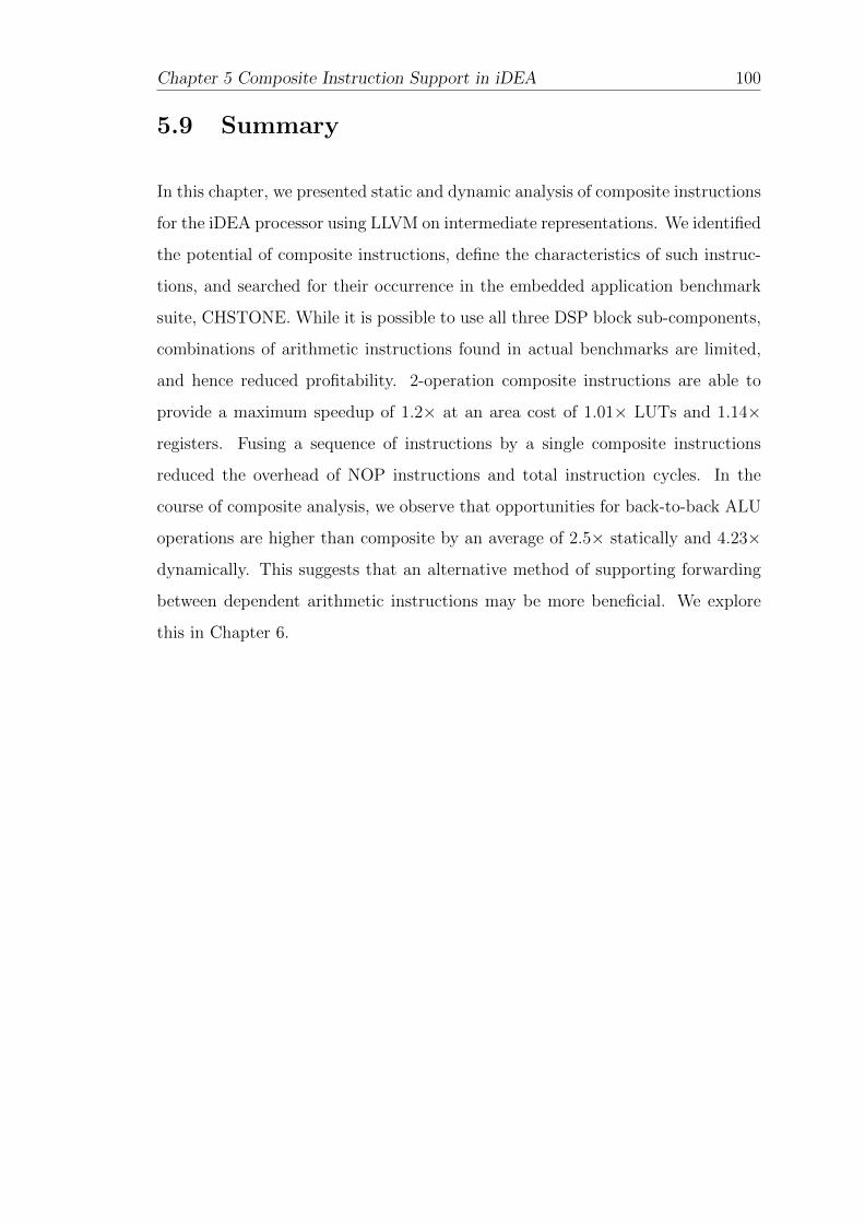
Chapter 5 Composite Instruction Support in iDEA 100
5.9 Summary
In this chapter, we presented static and dynamic analysis of composite instructions
for the iDEA processor using LLVM on intermediate representations. We identified
the potential of composite instructions, define the characteristics of such instruc-
tions, and searched for their occurrence in the embedded application benchmark
suite, CHSTONE. While it is possible to use all three DSP block sub-components,
combinations of arithmetic instructions found in actual benchmarks are limited,
and hence reduced profitability. 2-operation composite instructions are able to
provide a maximum speedup of 1.2× at an area cost of 1.01× LUTs and 1.14×
registers. Fusing a sequence of instructions by a single composite instructions
reduced the overhead of NOP instructions and total instruction cycles. In the
course of composite analysis, we observe that opportunities for back-to-back ALU
operations are higher than composite by an average of 2.5× statically and 4.23×
dynamically. This suggests that an alternative method of supporting forwarding
between dependent arithmetic instructions may be more beneficial. We explore
this in Chapter 6.

Chapter 6
Data Forwarding Using Loopback
Instructions
6.1 Introduction
In Chapter 3 and Chapter 4, we demonstrated how the flexibility of a DSP block
allows it to be leveraged as the execution unit of a general purpose processor.
However, as briefly discussed in Chapter 4, a deeply-pipelined, DSP block-based
scalar processor suffers significantly from the need to pad instructions with NOPs
to overcome data hazards. In this chapter, we perform a complete design space
exploration of a DSP block-based soft processor to understand the effect of pipeline
depth on frequency, area, and program runtime, noting the number of NOPs
required to resolve dependencies. We then present a restricted data forwarding
approach using a feedback path within the DSP block that allows for reduced NOP
padding.
The work presented in this chapter has previously appeared in:
• H. Y. Cheah, S. A. Fahmy, and N. Kapre, “On Data Forwarding in Deeply
Pipelined Soft Processors”, in Proceedings of the ACM/SIGDA International
101

Chapter 6 Data Forwarding Using Loopback Instructions 102
4 5 6 7 8 9 10 11 12 13 14 150
10 000
20 000
30 000
40 000
Pipeline Depth
Num
ber
ofN
OP
s
crc fib firmed mmul qsort
Figure 6.1: NOP counts as pipeline depth increases with no data forwarding.
Symposium on Field Programmable Gate Arrays (FPGA), Monterey, CA,
February 2015, pp. 181–189 [16].
• H. Y. Cheah, S. A. Fahmy, and N. Kapre “Analysis and Optimization of a
Deeply Pipelined FPGA Soft Processor”, in Proceedings of the International
Conference on Field Programmable Technology (FPT), Shanghai, China,
December 2014, pp. 235–238 [17].
6.2 Data Hazards in a Deeply Pipelined Soft Pro-
cessor
We have seen that deep pipelining of soft processor is necessary due to the pipeline
stages in the DSP block primitive. Even though this does result in higher fre-
quency, it increases the dependency window for data hazards, hence requiring
more NOPs for dependent instructions. A data hazard occurs when there is a
dependency between two instructions, and the overlap caused by pipelining would
affect the order the operands are accessed. Throughout this chapter, we use data
hazard to refer to read-after-write (RAW) hazards. RAW is the only type of haz-
ard observed in in-order, scalar processors. Figure 6.1 shows the rise in NOP

Chapter 6 Data Forwarding Using Loopback Instructions 103
7-Stage
IF IF ID EX EX EX WB
IF IF ID EX EX EX WB4 nops
8-Stage
IF IF ID EX EX EX EX WB
IF IF ID EX EX EX EX WB5 nops
9-Stage
IF IF IF ID ID EX EX EX WB
IF IF IF ID ID EX EX EX WB5 nops
Figure 6.2: Dependencies for pipeline depths of 7, 8 and 9 stages.
counts for a deeply-pipelined DSP block based soft processor, across a range of
benchmarks programs, as the pipeline depth is increased. We can see that the
NOPs become very significant as the pipeline depth increases. Figure 6.2 shows
pipeline depths of 7, 8 and 9 cycles, respectively, with fetch, decode, execute and
write back stages in each instruction pipeline and the number of NOPs required
to pad dependent instructions.
To achieve maximum frequency using a primitive like the DSP block, it must have
its multiple pipeline stages enabled. iDEA uses the DSP block as its execution
unit and a Block RAM as the instruction and data memory, and as a result, we
expect a long pipeline to be required to reach fabric frequency limits. By taking
a fine-grained approach to pipelining the remaining logic, we can ensure that we
balance delays to achieve high frequency. Since the pipeline stages in the DSP
block are fixed, arranging registers in different parts of the pipeline can have a
more pronounced impact on frequency.
To prevent a data hazard, an instruction dependent on the result of a previous
instruction must wait until the computed data is written back to the register
file before fetching operands. The second instruction can be fetched, but cannot
move to the decode stage (in which operands are fetched), until the instruction on
which it is dependent has written back its results. In the case of a 7-stage pipeline
with the pipeline configuration shown, 4 NOPs are required between dependent
instructions. Since there are many ways we can distribute processor pipeline cycles

Chapter 6 Data Forwarding Using Loopback Instructions 104
between the different stages, an increase in processor pipeline depth does not
always mean more NOPs are needed. Consider the 8 and 9-stage configurations in
Figure 6.2. Since the extra stage in the 9 cycle configuration is an IF stage, that can
be overlapped with a dependent instruction, no additional NOPs are required than
for the given 8 cycle configuration. This explains why the lines in Figure 6.1 do
not increase uniformly. However, due to the longer dependency window, a longer
pipeline depth with the same number of NOPs between consecutive dependent
instructions may still have a slightly higher total instruction count.
6.3 Related Work
A theoretical method for analyzing the effect of data dependencies on the perfor-
mance of in-order pipelines is presented in [149]. An optimal pipeline depth is
derived based on balancing pipeline depth and achieved frequency, with the help
of program trace statistics. A similar study for superscalar processors is presented
in [150]. Data dependency of sequential instructions can be resolved statically in
software or dynamically in hardware. Tomasulo’s algorithm allows instructions to
be executed out of order, where those not waiting for any dependencies are exe-
cuted earlier [151]. For dynamic resolution in hardware, extra functional units are
needed to handle the queuing of instructions and operands in reservation stations.
Additionally, handling out-of-order execution in hardware requires intricate haz-
ard detection and execution control. Synthesizing a basic Tomasulo scheduler [152]
on a Xilinx Virtex-6 yields an area consumption of 20× the size of a MicroBlaze,
and a frequency of only 84 MHz. This represents a significant overhead for a small
FPGA-based soft processor, and the overhead increases for deeper pipelines.
Data forwarding is a well-established technique in processor design, where results
from one stage of the pipeline can be accessed at a later stage sooner than would
normally be possible. This can increase performance by reducing the number of
NOP instructions required between dependent instructions. It has been explored
in the context of general soft processor design, VLIW embedded processors [153],

Chapter 6 Data Forwarding Using Loopback Instructions 105
as well as instruction set extensions in soft processors [154]. In each case, the
principle is to allow the result of an ALU computation to be accessed sooner than
would be possible in the case where write back must occur prior to execution of a
subsequent dependent instruction.
In this chapter, we show that the feedback path typically used for multiply-
accumulate operations allows us to implement an efficient forwarding scheme that
can significantly improve execution time in programs with dependencies, going be-
yond just multiply-add combinations. We compare this to an external forwarding
approach and the original design with no forwarding. Adding data forwarding to
iDEA decreases runtime by up to 25% across a range of small benchmarks, and
we expect similar gains in large benchmarks.
6.4 Managing Dependencies in Processor Pipelines
Data forwarding paths can help reduce the padding requirements between de-
pendent instructions, which are common in modern processors. However, a full
forwarding scheme typically allows forwarding from every succeeding stages of the
pipeline after the execute stage, and so can be costly since additional multiplexed
paths are required to facilitate this flexibility. With a longer pipeline, and more
possible forwarding paths, such an approach becomes infeasible for a lean, fast soft
processor. Some schemes provide forwarding paths that must then be exploited in
the assembly, while other dynamic approaches allow the processor to make these
decisions on the fly.
In our case, while dynamic forwarding, or even elaborate static forwarding would
be too complex, a restricted forwarding approach may be possible and could result
in a significant overall performance improvement. Rather than add a forwarding
path from every stage after the decode stage back to the execute stage inputs,
we can consider just a single path. In Table 6.1, we analyze the NOPs inserted
in more detail. Out of all the NOPs, we can see that a significant proportion
are between consecutive instructions with dependencies (4–30%). These could be

Chapter 6 Data Forwarding Using Loopback Instructions 106
Table 6.1: Dynamic cycle counts with 11-stage pipeline with % of NOPssavings.
BenchmarkTotalNOPs
ConsecutiveDependant
NOPs
ReducedConsecutiveDependant
NOPs
ReducedTotalNOPs
crc 22,808 7,200 (32%) 2,400 18,008 (−21%)
fib 4,144 816 (20%) 272 3,600 (−13%)
fir 46,416 5,400 (12%) 1,800 42,816 (−8%)
median 13,390 1,212 (9%) 404 12,582 (−6%)
qsort 28,443 1,272 (4%) 424 27,595 (−3%)
overcome by adding a single path allowing the result of an instruction to be used
as an operand in a subsequent instruction, avoiding the need for a writeback. We
propose adding a single forwarding path between the output of the execute stage,
and its input to allow this. Figure 6.4 shows how the addition of this path in a 9-
stage configuration would reduce the number of NOPs required before a subsequent
dependent instruction to just 2, compared to 5 in the case of no forwarding.
4 5 6 7 8 9 10 11 12 13 14 150
10
20
30
40
Pipeline Depth
%In
stru
ctio
nC
ount
Red
uct
ion
crc fib firmedian qsort
Figure 6.3: Reduced instruction count with data forwarding.
In Table 6.1, we show how the addition of this path reduces the number of NOPs
required to resolve such consecutive dependencies, and hence the reduction in

Chapter 6 Data Forwarding Using Loopback Instructions 107
IF IF IF ID ID EX EX EX WB
IF IF IF ID ID EX EX EX WB5 nops
(a) 9-Stage
IF IF IF ID ID EX EX EX WB
IF IF IF ID ID EX EX EX WB2 nops
(b) 9-Stage with External Forwarding
IF IF IF ID ID EX EX EX WB
IF IF IF ID ID EX EX EX WB
(c) 9-Stage with Internal Forwarding
Figure 6.4: Forwarding configurations, showing how subsequent instructioncan commence earlier in the pipeline.
overall NOPs required. As this fixed forwarding path is only valid for subsequent
dependencies, it does not eliminate NOPs entirely, and non-adjacent dependencies
are still subject to the same window. However, we can see a significant reduction
in the overall number of NOPs and hence, cycle count for execution of our bench-
marks across a range of pipeline depths. These savings are shown in Figure 6.3.
We can see significant savings of between 4 and 30% for the different benchmarks.
This depends on how often such chains of dependent instructions occur in the
assembly and how often they are executed.
6.5 Implementing Data Forwarding
In Figure 6.4 (a), we show the typical operation of an instruction pipeline without
data forwarding. In this case, a dependent instruction must wait for the previous
instruction to complete execution and the result to be written back to the register
file before commencing its decode stage. In this example, 5 clock cycles are wasted
to ensure the dependent instruction does not execute before its operand is ready.

Chapter 6 Data Forwarding Using Loopback Instructions 108
This penalty increases with the higher pipeline depths necessary for maximum
frequency operation on FPGAs.
6.5.1 External Data Forwarding
The naive approach to implementing data forwarding for such a processor would
be to pass the execution unit output back to its inputs. Since we cannot access
the internal stages of the DSP block from the fabric, we must pass the execution
unit output all the way back to the DSP block inputs. This external approach is
completely implemented in general purpose logic resources. In Figure 6.4 (b), this
is shown as the last execution stage forwarding its output to the first execution
stage of the next instruction, assuming the execute stage is 3 cycles long. This
still requires insertion of up to 2 NOPs between dependent instructions, depending
on how many pipeline stages are enabled for the DSP block (execution unit).
This feedback path also consumes fabric resources, and may impact achievable
frequency.
6.5.2 Proposed Internal Forwarding
Another possibility is to use the loopback path that is internal to the DSP block
to enable the result of a previous ALU operation to be ready as an operand in
the next cycle, eliminating the need to pad subsequent dependent instruction with
NOPs. The proposed loopback method is not a complete forwarding implementa-
tion as it does not support all instruction dependencies and only supports one-hop
dependencies. It still allows us to forward data when the immediate dependent
instruction is any ALU operation except a multiplication. Figure 6.4 (c) shows
the output of the execute stage being passed to the final cycle of the subsequent
instruction’s execute stage. In such a case, since the loopback path is built into the
DSP block, it does not affect achievable frequency or consume additional resource.

Chapter 6 Data Forwarding Using Loopback Instructions 109
Table 6.2: Opcode of loopback instructions
InstructionLoopback
Counterpart
Opcode Opcode
add 100000 add-lb 110000
and 100100 and-lb 110100
addi 001000 addi-lb 111000
ori 001101 ori-lb 111101
6.5.3 Instruction Set Modifications
We can identify loopback opportunities in software and a loopback indication can
be added to the encoded assembly instruction. We call these one-hop dependent
instructions that use a combination of multiply or ALU operation followed by
an ALU operation a loopback pair. For every arithmetic and logical instruction,
we add an equivalent loopback counterpart. The loopback instruction performs
the same operation as the original, except that it receives its operand from the
loopback path (i.e. previous output of the DSP block) instead of the register file.
As shown in Table 6.2, the loopback opcode is differentiated from the original
opcode by one bit difference for register arithmetic and two bit for immediate
instructions.
Moving loopback detection to the compilation flow keeps our hardware simple and
fast. In hardware loopback detection, circuitry is added at the end of execute,
memory access, and write back stages to compare the address of the destination
register in these stages and the address of source registers at the execute stage.
If the register addresses are the same, then the result is forwarded to the execute
stage. The cost of adding loopback detection for every pipeline stage after exe-
cute can be severe for deeply-pipelined processors, unnecessarily increasing area
consumption and delay. Instead, we opt for this one-size forwarding approach.

Chapter 6 Data Forwarding Using Loopback Instructions 110
A
B
FPGA Fabric
internal
P
DSP Block
external
Figure 6.5: Execution unit datapath showing internal loopback and externalforwarding paths.
6.6 DSP Block Loopback Support
Recall that the DSP block is composed of a multiplier and ALU along with regis-
ters and multiplexers that control configuration options. More recent DSP blocks
also contain a pre-adder allowing two inputs to be summed before entering the
multiplier. The ALU supports addition/subtraction and logic operations on wide
data. The required datapath configuration is set by a number of control inputs,
and these are dynamically programmable, which is the unique feature allowing use
of a DSP block as the execution unit in a processor [19].
When implementing digital filters using a DSP block, a multiply-accumulate oper-
ation is required, so the result of the final adder is fed back as one of its inputs in
the next stage using an internal loopback path, as shown in Figure 6.5. This path
is internal to the DSP block and cannot be accessed from the fabric, however the
decision on whether to use it as an ALU operand is determined by the OPMODE
control signal. The OPMODE control signal chooses the input to the ALU from
several sources: inputs to the DSP block, output of multiplier, or output of the
DSP block. When a loopback instruction is executed, the appropriate OPMODE
value instructs the DSP block to take one of its operands from the loopback path.
We take advantage of this path to implement data forwarding with minimal area
overhead.

Chapter 6 Data Forwarding Using Loopback Instructions 111
6.7 DSP ALU Multiplexers
A
B
M PA
B
C C
P
30
18
48
48
18
48
48
25
INMODEALUMODEOPMODE
X
Y
Z
Figure 6.6: Multiplexers selecting inputs from A, B, C and P.
The OPMODE control signal chooses the input to ALU using a set of pre-ALU
multiplexers. As shown in a detailed Figure 6.6, the output of the DSP block can
be fed back to the ALU through two paths: multiplexer X or Z. We use multiplexer
X to minimize changes to our existing decoder configurations. Irrespective of the
arithmetic operation performed, the feedback path is consistent for all loopback
instructions.
While using one feedback path simplifies control complexity, it incurs the con-
straint of using only instructions with dependent second operand as a loopback
instruction. Instructions with dependent first operand are not supported. To
maximize the pool of loopback instructions, we swap the position of dependent
first operand with the second operand. Addition and logical operations are com-
mutative, and hence the result is not affected by the order of inputs. Swapping
is applied to all dependent consecutive arithmetic instructions except subtraction,
which is non-commutative.

Chapter 6 Data Forwarding Using Loopback Instructions 112
Algorithm 1: Loopback analysis algorithm.Data: AssemblyResult: LoopbackAssembly<vector>w ← Number of pipeline stages − number of IF stages;for i ← 0 to size(Assembly) do
window ← 0;DestInstr ← Assembly[i];for j ← 1 to w-1 do
SrcInstr ← Assembly[i− j];if depends(SrcInstr,DestInstr) then
loopback ← true;depth ← j;break;
end
endfor j ← 0 to w-1 do
if loopback thenLoopbackAssembly.push back(Assembly[i] | LOOPBACK MASK) ;
endelse
LoopbackAssembly.push back(Assembly[i]);for k ← 0 to j-1 do
LoopbackAssembly.push back(NOP);end
end
end
end
6.8 NOP-Insertion Software Pass
Dependency analysis to identify loopback opportunities is done in the compiler’s
assembly. For dependencies that cannot be resolved with this forwarding path,
sufficient NOPs are inserted to overcome hazards. When a subsequent dependent
arithmetic operation follows its predecessor, it can be tagged as a loopback instruc-
tion, and no NOPs are required for this dependency. For the external forwarding
approach, the number of NOPs inserted between two dependent instructions de-
pends on the DSP block’s pipeline depth (the depth of the execute stage). We
call this the number of ALU NOPs. A summary of this analysis scheme is shown
in Algorithm 1. We analyze the generated assembly for loopback opportunities
with a simple linear-time heuristic. We scan the assembly line-by-line and mark
dependent instructions within the pipeline window. These instructions are then

Chapter 6 Data Forwarding Using Loopback Instructions 113
converted by the assembler to include a loopback indication flag in the instruction
encoding. We also insert an appropriate number of NOPs to take care of other
dependencies.
After NOPs are inserted in the appropriate locations in the instruction list, all
branch and jump targets are re-evaluated. Insertion of extra NOP instructions
modifies the instruction sequence, affecting the address of existing instructions.
Updating the target address of branch and jump instructions ensures that when
program control changes, the correct target instruction is fetched. Additionally,
branch and jump targets are checked for dependencies across program control
changes (i.e. branch is taken), and if necessary, may require additional NOPs to
be inserted.
6.9 Experiments
Hardware: We implement the modified design on a Xilinx Virtex-6 XC6VLX240T-
2 FPGA (ML605 platform) using Xilinx ISE 14.5 tools. We use area constraints to
help ensure high clock frequency and area-efficient implementation. We generate
various processor combinations to support pipeline depths from 4–15. We bench-
mark the performance of our processor using the instruction count when executing
embedded C benchmarks. Input test vectors are contained in the source files and
the computed output is checked against a hard-coded golden reference, thereby
simplifying verification. For experimental purposes, the pipeline depth is made
variable through a parameterizable shift register at the output of each processor
stage. During automated implementation runs in ISE, the shift register parame-
ter is incremented, increasing the pipeline depth. Based on the input parameter,
the number of shift registers are generated by a for loop statement in the HDL.
The default shift register size is 1. We enable retiming and register balancing to
exploit the extra registers in the datapath. With these options, the registers are
moved forward or backward in the logic circuit to improve timing. In addition to
register balancing, we enable shift register extraction options. In a design where

Chapter 6 Data Forwarding Using Loopback Instructions 114
the ratio of registers is high, and shift registers are abundant, this option helps
balance LUT and register usage. ISE synthesis and implementation options are
consistent throughout all the experimental runs.
Parametric Verilog
Constraints
XilinxISE
BenchmarkC code
LLVMMIPS
Area
Freq.
Cycles
LoopbackAnalysis
Functional Simulator
RTL SimulatorAssembler
FPGADriver
ML605Platform
In-System Execution
Figure 6.7: Experimental flow.
Compiler: We generate assembly code for the processor using the LLVM- MIPS
backend. We use a post-assembly pass to identify opportunities for data forward-
ing and modify the assembly accordingly, as discussed in Section 6.8. We verify
functional correctness of our modified assembly code using a customized simulator
for internal and external loopback, and run RTL ModelSim simulations of actual
hardware to validate different benchmarks. We repeat our validation experiments
for all pipeline depth combinations. We show a high-level view of our experimental
flow in Figure 6.7.
In-System Verification: Finally, we test our processor on the ML605 board for
sample benchmarks to demonstrate functional correctness in silicon. The commu-
nication between the host and FPGA is managed using the open source FPGA
interface framework in [155]. We verify correctness by comparing the data memory
contents at the end of functional and RTL simulation, and in-FPGA execution.

Chapter 6 Data Forwarding Using Loopback Instructions 115
4 5 6 7 8 9 10 11 12 13 14 15
200
250
300
350
400
450
500
Pipeline Depth
Fre
quen
cy(M
Hz)
Figure 6.8: Frequency of different pipeline combinations with internal loop-back.
6.9.1 Area and Frequency Analysis
Since the broad goal of iDEA is to maximize soft processor frequency while keep-
ing the processor small, we perform a design space exploration to help pick the
optimal combination of pipeline depths for the different stages. We vary the num-
ber of pipeline stages from 1–5 for each stage: fetch, decode, and execute, and the
resulting overall pipeline depth is 4–15 (the writeback stage is fixed at 1 cycle).
Impact of Pipelining: Figure 6.8 shows the frequency achieved for varying
pipeline depths between 4–15 for a design with internal loopback enabled. Each
depth configuration represents several processor combinations as we can distribute
these registers in different parts of the 4-stage pipeline. The line traces points that
achieve the maximum frequency for each pipeline depth. The optimal combination
of stages, that results in the highest frequency for each depth, is presented in
Table 6.3.
While frequency increases considerably up to 10 stages, beyond that, the increases
are modest. This is expected as we approach the raw fabric limits around 500 MHz.
For each overall pipeline depth, we have selected the combination of pipeline
stages that yields the highest frequency for all experiments. With an increased

Chapter 6 Data Forwarding Using Loopback Instructions 116
Table 6.3: Optimal combination of stages and associated NOPs at eachpipeline depth (WB = 1 in all cases)
Depth IF ID EX NOPs ALUNOPs
4 1 1 1 2 0
5 1 2 1 3 0
6 2 2 1 3 0
7 2 1 3 4 2
8 2 2 3 5 2
9 2 2 4 6 2
10 3 2 4 6 2
11 3 2 5 7 2
12 3 3 5 8 2
13 4 3 5 8 2
14 5 3 5 8 2
15 4 5 5 10 2
pipeline depth, we must now pad dependent instructions with more NOPs, so these
marginal frequency benefits can be meaningless in terms of wall clock time for an
executed program. In Figure 6.4, we illustrated how a dependent instruction must
wait for the previous result to be written back before its instruction decode stage.
This results in required insertion of 5 NOPs for that 8 stage pipeline configura-
tion. For each configuration, we determine the required number of NOPs to pad
dependent instructions, as detailed in Table 6.3. For external forwarding, when
the execute stage is 0 6 K 6 3 cycles, we need K − 1 NOPs between depen-
dent instructions, which we call ALU NOPs. When the execute stage depth is
larger than 3, the number of ALU NOPs required stays constant at 2, as the DSP
pipeline depth does not increase beyond 3 despite the increasing pipeline depth
for the execute stage.
Figure 6.9 shows the distribution of LUT and register consumption for all imple-
mented combinations. Register consumption is generally higher than LUT con-
sumption, and this becomes more pronounced in the higher frequency designs.
Figure 6.10 shows a comparison of resource consumption between the designs with
no forwarding, internal loopback, and external forwarding. External forwarding
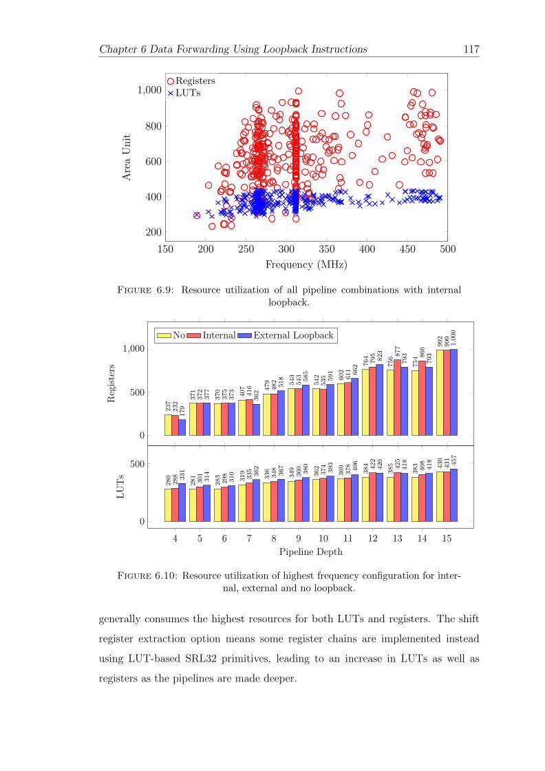
Chapter 6 Data Forwarding Using Loopback Instructions 117
150 200 250 300 350 400 450 500
200
400
600
800
1,000
Frequency (MHz)
Are
aU
nit
RegistersLUTs
Figure 6.9: Resource utilization of all pipeline combinations with internalloopback.
0
500
1,000
237
371
370
407 479 543
542 602
764
756
754
992
232
372
375
416 482 543
535 611
795 877
866
990
179
377
373
362
518 585
591 662
823
793
793
1,000
Reg
iste
rs
No Internal External Loopback
4 5 6 7 8 9 10 11 12 13 14 15
0
500
280
281
283 319
336
349
362
369
384
385
383 430
288
301
298 335
348
360
374
378 422
425
408
431
331
314
310 362
367
380
393
406
420
418
418 457
Pipeline Depth
LU
Ts
Figure 6.10: Resource utilization of highest frequency configuration for inter-nal, external and no loopback.
generally consumes the highest resources for both LUTs and registers. The shift
register extraction option means some register chains are implemented instead
using LUT-based SRL32 primitives, leading to an increase in LUTs as well as
registers as the pipelines are made deeper.

Chapter 6 Data Forwarding Using Loopback Instructions 118
4 5 6 7 8 9 10 11 12 13 14 15150
200
250
300
350
400
450
500
Pipeline Depth
Fre
quen
cy(M
Hz)
InternalExternal
Figure 6.11: Frequency with internal loopback and external forwarding.
Impact of Loopback: Implementing internal loopback forwarding proves to have
a minimal impact on area, of under 5%. External forwarding generally uses slightly
more resources, though the difference is not constant. External forwarding does
lag internal forwarding in terms of frequency for all pipeline combinations, as
shown in Figure 6.11, however, the difference diminishes as frequency saturates
at the higher pipeline depths. Though we must also consider the NOP penalty of
external forwarding over internal loopback.
6.9.2 Execution Analysis
Static Analysis: In Table 6.4, we show the percentage of occurrences of con-
secutive loopback instructions in each benchmark program. Programs that show
high potential are those that have multiple independent occurrences of loopback
pairs, or long chains of consecutive loopback pairs. Independent pairs of loopback
instructions are common in most programs, however for crc and fib, we can find
a chain of up to 3 and 4 consecutive loopback pairs respectively.
Dynamic Analysis: In Table 6.5, we show the actual execution cycle counts
without forwarding, with external forwarding, and with internal loopback, as well

Chapter 6 Data Forwarding Using Loopback Instructions 119
Table 6.4: Static cycle counts with and without loopback for a 10-cyclepipeline with % savings.
Benchmark
TotalInst.
Loopback
Inst. %
crc 32 3 9
fib 40 4 10
fir 121 1 0.8
median 132 11 8
mmult 332 3 0.9
qsort 144 10 7
Table 6.5: Dynamic cycle counts with and without loopback for a 10-cyclepipeline with % savings.
Benchmark
Loopback
Without External % Internal %
crc 28,426 22,426 21 20,026 29
fib 4,891 4,211 14 3,939 19
fir 2,983 2,733 8 2,633 11
median 1,5504 14,870 4 14,739 5
mmult 1,335 1,322 0.9 1,320 1
qsort 32,522 30,918 5 30,386 7
as the percentage of executed instructions that use the loopback capability. Al-
though fib offers the highest percentage of loopback occurrences in static analysis,
in actual execution, crc achieves the highest savings due to the longer loopback
chain, and the fact that the loopback-friendly code is run more frequently.
Internal Loopback: In Figure 6.12, we show the Instructions per Cycle (IPC)
savings for a loopback-enabled processor over the non-forwarding processor, as
we increase pipeline depth. Most benchmarks have IPC improvements between
5–30% except the mmult benchmark. For most benchmarks, we note resilient
improvements across pipeline depths. From Table 6.5 we can clearly correlate the
IPC improvements with the predicted savings.

Chapter 6 Data Forwarding Using Loopback Instructions 120
4 5 6 7 8 9 10 11 12 13 14 150
5
10
15
20
25
30
35
Pipeline Depth
%IP
CSav
ings
crc fib firmedian mmult qsort
Figure 6.12: IPC improvement when using internal DSP loopback.
4 5 6 7 8 9 10 11 12 13 14 150
5
10
15
20
25
30
35
Pipeline Depth
%IP
CSav
ings
crc fib firmedian mmult qsort
Figure 6.13: IPC improvement when using external loopback.
External Loopback: Figure 6.13 shows the same analysis for external forward-
ing. It is clear that external forwarding is not as improved as internal loopback,
since we do not totally eliminate NOPs in chains of supported loopback instruc-
tions. For pipeline depths of 4–6, the IPC savings for internal and external loop-
back are equal, since the execute stage is 1 cycle (refer to Table 6.3), and hence

Chapter 6 Data Forwarding Using Loopback Instructions 121
14
16
18
20
22
24
26
28
30
Tim
e(u
s)
4 5 6 7 8 9 10 11 12 13 14 15
200
250
300
350
400
450
500
Pipeline Depth
Fre
quen
cy(M
Hz)
FrequencyNo ForwardingInternal Loopback
Figure 6.14: Frequency and geomean wall clock time with and without internalloopback enabled.
14
16
18
20
22
24
26
28
30
Tim
e(u
s)
4 5 6 7 8 9 10 11 12 13 14 15
200
250
300
350
400
450
500
Pipeline Depth
Fre
quen
cy(M
Hz)
Frequency (Int)
Frequency (Ext)Internal LoopbackExternal Forwarding
Figure 6.15: Frequency and geomean wall clock time on designs incorporatinginternal loopback and external forwarding.
neither forwarding method requires NOPs between dependent instructions. As
a result of the extra NOP instructions, the IPC savings decline marginally in
Figure 6.13 and stay relatively low.
Impact of Internal Loopback on Wall-Clock Time Figure 6.14 shows nor-
malized wall-clock times for the different benchmarks. We expect wall-clock time

Chapter 6 Data Forwarding Using Loopback Instructions 122
to decrease as we increase pipeline depth up to a certain limit. At sufficiently
high pipeline depths, we expect the overhead of NOPs to cancel the diminishing
improvements in operating frequency. There is an anomalous peak at 9 stages
due to a more gradual frequency increase, visible in Figure 6.8, along with a con-
figuration with a steeper ALU NOP count increase as shown in Table 6.3. The
10-cycle pipeline design gives the lowest execution time for both internal loopback
and non-loopback. Such a long pipeline is only feasible when data forwarding is
implemented, and our proposed loopback approach is ideal in such a case, as we
can see from the average 25% improvement in runtime across these benchmarks.
Comparing External Forwarding and Internal Loopback Figure 6.15 shows
the maximum frequency and normalized wall clock times for for internal loopback
and external forwarding. As previously discussed, external forwarding results in
higher resource utilization and reduced frequency. At 4–6 cycle pipelines, the lower
operating frequency of the design for external forwarding results in a much higher
wall-clock time for the benchmarks. While the disparity between external and
internal execution time is significant at shallower pipeline depths, the gap closes
as depth increases. This is due to the saturation of frequency at pipeline depths
greater than 10 cycles and an increase in the insertion of ALU NOPs. The 10-cycle
pipeline configuration yields the lowest execution time for all three designs, with
internal loopback achieving the lowest execution time.
6.10 Summary
In this chapter, we expanded the role of the DSP block further by exploiting
the internal loopback path typically used for multiply accumulate operations as
a data forwarding path. This allows dependent ALU instructions to immediately
follow each other, eliminating the need for padding NOPs. Full forwarding can be
prohibitively complex for a lean soft processor, so we explored two approaches: an
external forwarding path around the DSP block execution unit in FPGA logic and
using the intrinsic loopback path within the DSP block primitive. We showed that

Chapter 6 Data Forwarding Using Loopback Instructions 123
internal loopback improves performance by 5% compared to external forwarding,
and up to 25% over no data forwarding. We also showed how the optimal pipeline
depth of 10 stages is selected for iDEA by performing a full design space exploration
on pipeline combinations and frequency, then choosing the combination with the
highest frequency and lowest execution time. The result is a processor that runs
at a frequency close to the fabric limit of 500 MHz, but without the significant
dependency overheads typical of such processors.

Chapter 7
Conclusions and Future Work
FPGAs are increasingly used to implement complex hardware designs in self-
contained embedded systems, but the complex and time-consuming design pro-
cess has proven to be a significant obstacle to wider adoption. Soft processors
can enable the design of overlay architectures that function as an intermediate
fabric for application mapping. Optimizing the soft processor, which is the basic
building block of an overlay, is therefore paramount to the design of high perfor-
mance overlay architectures. When soft processors are designed in a manner that
is device-agnostic, they consume significant area and run slowly. An architecture-
oriented soft processor design has the potential to offer an abstraction of the FPGA
architecture that does not entail significant area and performance overheads.
In this thesis, we showed how an application specific hard resource, the DSP block,
can be used as a key building block in the design of a lean, fast soft processor.
Being optimized for basic arithmetic operations, and most importantly, offering
dynamic programmability, makes the DSP block an idea enabler for such a design,
condensing a significant amount of functionality into an optimized hard block.
This means fewer general purpose resources are needed to build the remainder
of the processor and performance can be maximized. We showed that using the
DSP block as the key component in a soft processor enabled a design that could
run at close to the DSP block’s theoretical maximum frequency of 500MHz on
a Xilinx Virtex 6. We showed how using the DSP block only through inference
124

Chapter 7 Conclusions and Future Work 125
in synthesis failed to offer similar benefits. Most important to this achievement
are the dynamically programmable control inputs that enable the DSP block to
be used in a flexible manner to support a range of instructions, changeable on a
cycle-by-cycle basis, rather than just for multiplication as is typical when inferred
in synthesis.
We detailed the design of the iDEA soft processor and evaluated its capabili-
ties and performance with C microbenchmarks and the CHSTONE suite, using a
cycle-accurate simulator and hardware RTL simulations, along with validation on
an FPGA. We learnt that one drawback of using primitives like the DSP block is
the long processor pipeline they require to reach maximum frequency. This results
in long dependency windows that must typically be overcome using empty idle in-
structions (NOPs), and hence longer runtimes. These longer pipelines also result in
increasing register usage, with minimal additional LUT usage. We demonstrated
two ways to overcome this problem. In the first we showed that the DSP block’s
ability to support composite instructions could help reduce this effect by chain-
ing together supported subsequent dependent instructions into single composite
instructions. However, given the limited number of supported pairs, the benefits
were inconsistent across benchmarks, with a mean 4% improvement in runtime.
An alternative solution, exploiting the feedback path in the DSP block as a data
forwarding path, offered more substantial improvements of 25% in runtime over
no forwarding. We also explored the concept of instruction set subsetting, where
only a portion of the overall instruction set is enabled, as required for a particular
application. We found that this had minimal impact on area, as the decoding
logic is of minimal size and most of the resources are used to implement the deep
pipeline. The design of iDEA has demonstrated the more widespread applicability
of flexible DSP blocks in general purpose computing, with a compact, lean design
that comes close to the performance limits of the FPGA fabric. We are confident
that this important contribution can enable a range of future research on soft
overlay architectures for FPGAs.
In this thesis, we have made the following contributions:

Chapter 7 Conclusions and Future Work 126
1. The iDEA FPGA Soft Processor – A DSP block based soft processor was
designed, implemented, and mapped to a Xilinx Virtex-6 XC6VLX240T-2
FPGA. The processor leverages the DSP48E1 to support standard arithmetic
instructions, as well as other instructions suited to the primitive’s DSP roots,
focusing on using as little fabric logic as possible. We tested our processor
on the ML605 board to demonstrate functional correctness.
2. Parameterized Customizable Hardware Design – To take advantage
of the FPGA programmable fabric, we used a parameterized design to allow
finer control over pipeline depth, DSP block functionality (e.g. pre-adder),
memory size and instruction set. This allows the iDEA architecture to be
tailored to requirements. A bit mask can be used to disable unneeded in-
structions, reducing area overheads.
3. Design Space Exploration – To study the performance cost of pipelining
in soft processors, we performed a full design space exploration of iDEA to
examine the effect of pipeline depth on frequency, area and execution time.
To achieve this, the pipeline depth was made variable through a parameter-
ized shift register at the output of each processor stage, allowing iDEA to
be configured with depths from 4 – 15 stages, and we showed an achievable
frequency of 500 MHz at pipeline depth of 10 stages onwards.
4. Pseudo-Boolean Satisfiability Model – We developed a SAT-based pseudo-
boolean optimization to identify the subset of feasible instruction pairs that
can be combined into composite instructions while considering instruction
dependencies. Using this approach, we isolated instructions that are fusable
while at the same time maximizing the number of composite instructions
sequences.
5. Restricted Data Forwarding Approach – To address the long depen-
dency chains due to iDEA’s deep pipeline, we explored the possible benefits
of a restricted forwarding approach. We showed that the feedback path typ-
ically used for multiply-accumulate operations in DSP blocks can be used to
implement a more efficient forwarding scheme that can significantly improve

Chapter 7 Conclusions and Future Work 127
performance of programs with dependencies. The result was an increase in
effective IPC, and 5 – 30% (mean 25%) improvement in wall clock time com-
pared to no forwarding and a 5% improvement when compared to external
forwarding.
In conclusion, a soft processor that fully exploits the capabilities of the underly-
ing hardware offers much improved performance and area. By taking advantage
of the dynamic programmability features of the DSP block, we designed a fast,
tiny soft processor with extensible composite functionality and data forwarding.
Using the optimized arithmetic DSP block as the execution unit minimizes the
use of fabric logic. Other features of the DSP block that aided in the design
of iDEA are the arithmetic sub-components (i.e. pre-adder, multiplier) and the
multiply-accumulate feedback path. By designing a soft processor around the DSP
architecture, we obtained a design that could run close to the DSP block maximum
frequency of 500MHz.
7.1 Future Work
Our work was intended to propose a new soft processor that offers the performance
and area benefits of an architecture-centric design, while taking advantage of the
generally unused dynamic programmability of the DSP block. A single processor,
however, does not offer us best use of a whole FPGA, nor performance comparable
with a custom hardware design. A key direction for future work is to see how such
a processor can be incorporated into a higher level parallel system architecture.
We have identified a number of possibilities.
1. Chaining of DSP blocks – Although the current design method of using
only one DSP block has proven to be functionally sufficient, cascading two
DSP blocks could possibly create more opportunities for composite instruc-
tions. Current composite instructions allow fusing of arithmetic operations
such as add, subtract and multiply in a single instruction, but chaining two

Chapter 7 Conclusions and Future Work 128
DSP blocks together as an execution unit extends the set further to include
logical operations. Cascading of two DSP blocks comes at no extra cost, as
the cascade path is a part of the primitive itself. However, cascading may
require modifications to the pipeline to accommodate the second DSP block.
2. IR Transformation – Our IR analysis shows promising potential for form-
ing composite and loopback instructions. However, the analysis is limited
to identification of possible candidates. Transformations could be applied
at the IR stage to re-arrange the sequence of instructions to expose more
feasible candidates for fusing or forwarding, thereby increasing performance
further.
3. Tiling of multiple iDEA processors – As iDEA is designed to occupy
minimal logic with only one DSP block per processor, a single Virtex-6 240T
could potentially host as many as 400 iDEA processors (excluding commu-
nication and interconnect overheads). A parallel array of these lightweight
soft processor could offer a feasible architecture for compute-intensive paral-
lel tasks. iDEA could be applied to a variety of FPGA overlay approaches.

Appendices
129
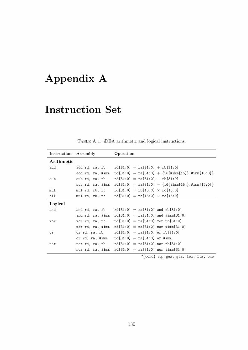
Appendix A
Instruction Set
Table A.1: iDEA arithmetic and logical instructions.
Instruction Assembly Operation
Arithmetic
add add rd, ra, rb rd[31:0] = ra[31:0] + rb[31:0]
add rd, ra, #imm rd[31:0] = ra[31:0] + {16{#imm[15]},#imm[15:0]}sub sub rd, ra, rb rd[31:0] = ra[31:0] − rb[31:0]
sub rd, ra, #imm rd[31:0] = ra[31:0] − {16{#imm[15]},#imm[15:0]}mul mul rd, rb, rc rd[31:0] = rb[15:0] × rc[15:0]
sll mul rd, rb, rc rd[31:0] = rb[15:0] × rc[15:0]
Logical
and and rd, ra, rb rd[31:0] = ra[31:0] and rb[31:0]
and rd, ra, #imm rd[31:0] = ra[31:0] and #imm[31:0]
xor xor rd, ra, rb rd[31:0] = ra[31:0] xor rb[31:0]
xor rd, ra, #imm rd[31:0] = ra[31:0] xor #imm[31:0]
or or rd, ra, rb rd[31:0] = ra[31:0] or rb[31:0]
or rd, ra, #imm rd[31:0] = ra[31:0] or #imm
nor nor rd, ra, rb rd[31:0] = ra[31:0] nor rb[31:0]
nor rd, ra, #imm rd[31:0] = ra[31:0] nor #imm[31:0]
*{cond} eq, gez, gtz, lez, ltz, bne
130
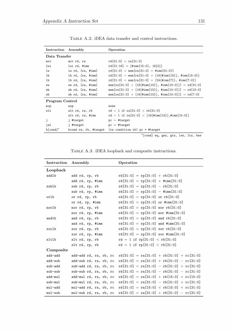
Appendix A Instruction Set 131
Table A.2: iDEA data transfer and control instructions.
Instruction Assembly Operation
Data Transfer
mov mov rd, ra rd[31:0] = ra[31:0]
lui lui rd, #imm rd[31:16] = {#imm[15:0], 16{0}}lw lw rd, [ra, #imm] rd[31:0] = mem[ra[31:0] + #imm[31:0]]
lh lh rd, [ra, #imm] rd[31:0] = mem[ra[31:0] + {16{#imm[15]}, #imm[15:0]}lb lb rd, [ra, #imm] rd[31:0] = mem[ra[31:0] + {24{#imm[7]}, #imm[7:0]}sw sw rd, [ra, #imm] mem[ra[31:0] + {16{#imm[15]}, #imm[15:0]}] = rd[31:0]
sh sh rd, [ra, #imm] mem[ra[31:0] + {16{#imm[15]}, #imm[15:0]}] = rd[15:0]
sb sb rd, [ra, #imm] mem[ra[31:0] + {16{#imm[15]}, #imm[15:0]}] = rd[7:0]
Program Control
nop nop none
slt slt rd, ra, rb rd = 1 if ra[31:0] < rb[31:0]
slt rd, ra, #imm rd = 1 if ra[31:0] < {16{#imm[15]},#imm[15:0]}j j #target pc = #target
jal j #target pc = #target
b{cond}* bcond ra, rb, #target (ra condition rb) pc = #target
*{cond} eq, gez, gtz, lez, ltz, bne
Table A.3: iDEA loopback and composite instructions.
Instruction Assembly Operation
Loopback
addlb add rd, rp, rb rd[31:0] = rp[31:0] + rb[31:0]
add rd, rp, #imm rd[31:0] = rp[31:0] + #imm[31:0]
sublb sub rd, rp, rb rd[31:0] = rp[31:0] − rb[31:0]
sub rd, rp, #imm rd[31:0] = rp[31:0] − #imm[31:0]
orlb or rd, rp, rb rd[31:0] = rp[31:0] or rb[31:0]
or rd, rp, #imm rd[31:0] = rp[31:0] or #imm[31:0]
norlb nor rd, rp, rb rd[31:0] = rp[31:0] nor rb[31:0]
nor rd, rp, #imm rd[31:0] = rp[31:0] nor #imm[31:0]
andlb and rd, rp, rb rd[31:0] = rp[31:0] and rb[31:0]
and rd, rp, #imm rd[31:0] = rp[31:0] and #imm[31:0]
xorlb xor rd, rp, rb rd[31:0] = rp[31:0] xor rb[31:0]
xor rd, rp, #imm rd[31:0] = rp[31:0] xor #imm[31:0]
sltlb slt rd, rp, rb rd = 1 if rp[31:0] < rb[31:0]
slt rd, rp, rb rd = 1 if rp[31:0] < rb[31:0]
Composite
add-add add-add rd, ra, rb, rc rd[31:0] = ra[31:0] + rb[31:0] + rc[31:0]
add-sub add-sub rd, ra, rb, rc rd[31:0] = ra[31:0] + rb[31:0] − rc[31:0]
sub-add sub-add rd, ra, rb, rc rd[31:0] = ra[31:0] − rb[31:0] + rc[31:0]
sub-sub sub-sub rd, ra, rb, rc rd[31:0] = ra[31:0] − rb[31:0] − rc[31:0]
add-mul add-mul rd, ra, rb, rc rd[31:0] = ra[31:0] + rb[15:0] × rc[15:0]
sub-mul sub-mul rd, ra, rb, rc rd[31:0] = ra[31:0] − rb[31:0] + rc[31:0]
mul-add mul-add rd, ra, rb, rc rd[31:0] = ra[15:0] × rb[15:0] + rc[31:0]
mul-sub mul-sub rd, ra, rb, rc rd[31:0] = ra[31:0] + rb[31:0] − rc[31:0]
Appendix B
DSP Configurations
132

Appendix B DSP Configurations 133
Table B.1: DSP configurations in iDEA.
Operation INMODE OPMODE ALUMODE
ADD 00000 0110011 0000
ADDLB 00000 0110010 0000
ADDU 00000 0110011 0000
ADDULB 00000 0110010 0000
AND 00000 0110011 1100
ANDLB 00000 0110010 1100
MULT 10001 0000101 0000
MULTU 10001 0000101 0000
MFHI 00000 0110011 0000
MFLO 00000 0110011 0000
MTHI 00000 0110011 0000
MTLO 00000 0110011 0000
NOR 00000 0111011 1110
NORLB 00000 0111010 1110
OR 00000 0111011 1100
ORLB 00000 0111010 1100
SLL 10001 0000101 0000
SLLV 10001 0000101 0000
SLT 00000 0110011 0011
SLTLB 00000 0110010 0011
SLTU 00000 0110011 0011
SLTULB 00000 0110010 0011
SRL 10001 0000101 0000
SRA 10001 0000101 0000
SRAV 10001 0000101 0000
SRLV 10001 0000101 0000
SUB 00000 0110011 0011
SUBLB 00000 0110011 0011
SUBU 00000 0110011 0011
SUBULB 00000 0110011 0011
XOR 00000 0110011 0100
XORLB 00000 0110010 0100
ADDI 00000 0110011 0000
ADDILB 00000 0110010 0000
ADDIU 00000 0110011 0000
ADDIULB 00000 0110010 0000
ANDI 00000 0110011 1100
ANDILB 00000 0110010 1100
BEQ 00000 0110011 0011
BGEZ 00000 0110000 0011
BGTZ 00000 0110000 0011
BLEZ 00000 0110000 0011
BNE 00000 0110011 0011
LUI 00000 0000011 0000
ORI 00000 0111011 1100
ORILB 00000 0111010 1100
SLTI 00000 0110011 0011
SLTILB 00000 0110010 0011
SLTIU 00000 0110011 0011
SLTIULB 00000 0110010 0011
XORI 00000 0110011 0100
XORILB 00000 0110010 0100
JAL 00000 0110011 0000

Bibliography
[1] J. L. Hennessy and D. A. Patterson, Computer Architecture: A Quantitative
Approach. Morgan Kaufmann, 1990.
[2] Y. Hara, H. Tomiyama, S. Honda, and H. Takada, “Proposal and quantita-
tive analysis of the CHStone benchmark program suite for practical C-based
high-level synthesis,” in Journal of Information Processing, 2009.
[3] G. Stitt and J. Coole, “Intermediate Fabrics: Virtual Architectures for Near-
Instant FPGA Compilation,” Embedded Systems Letters, IEEE, vol. 3, no. 3,
pp. 81–84, 2011.
[4] A. K. Jain, D. L. Maskell, and S. A. Fahmy, “Throughput oriented FPGA
overlays using DSP blocks,” in Proceedings of the Design, Automation and
Test in Europe Conference (DATE), pp. 1628–1633, 2016.
[5] A. K. Jain, D. L. Maskell, and S. A. Fahmy, “Efficient overlay architecture
based on DSP blocks,” in Proceedings of the IEEE International Symposium
on Field Programmable Custom Computing Machines (FCCM), pp. 25–28,
2015.
[6] A. K. Jain, X. Li, S. A. Fahmy, and D. L. Maskell, “Adapting the DySER
architecture with DSP blocks as an overlay for the Xilinx Zynq,” ACM
SIGARCH Computer Architecture News, vol. 43, no. 4, pp. 28–33, 2015.
[7] Altera Corp., Nios II Processor Design, 2011.
[8] Xilinx Inc., UG984: MicroBlaze Processor Reference Guide, 2014.
134

BIBLIOGRAPHY 135
[9] K. Vipin and S. A. Fahmy, “A high speed open source controller for FPGA
partial reconfiguration,” in Proceedings of the International Conference on
Field-Programmable Technology, pp. 61–66, 2012.
[10] N. Kapre and A. DeHon, “VLIW-SCORE: Beyond C for sequential control of
SPICE FPGA acceleration,” in Proceedings of the International Conference
on Field Programmable Technology, Dec. 2011.
[11] Aeroflex Gaisler, GRLIB IP Library User’s Manual, 2012.
[12] Xilinx Inc., UG369: Virtex-6 FPGA DSP48E1 Slice User Guide, 2011.
[13] F. De Dinechin and B. Pasca, “Designing Custom Arithmetic Data Paths
with FloPoCo,” IEEE Design & Test of Computers, vol. 28, no. 4, pp. 18–27,
2011.
[14] S. Xu, S. A. Fahmy, and I. V. McLoughlin, “Square-rich fixed point polyno-
mial evaluation on FPGAs,” in Proceedings of International Symposium on
Field Programmable Gate Arrays, 2014.
[15] B. Ronak and S. A. Fahmy, “Mapping for maximum performance on FPGA
DSP blocks,” IEEE Transactions on Computer Aided Design of Integrated
Circuits and Systems, vol. 35, no. 4, pp. 573–585, 2016.
[16] H. Y. Cheah, S. A. Fahmy, and N. Kapre, “On Data Forwarding in Deeply
Pipelined Soft Processors,” in Proceedings of the International Symposium
on Field-Programmable Gate Arrays, pp. 181–189, ACM, 2015.
[17] H. Y. Cheah, S. A. Fahmy, and N. Kapre, “Analysis and Optimization of a
Deeply Pipelined FPGA Soft Processor,” in Proceedings of the International
Conference on Field Programmable Technology, pp. 235–238, 2014.
[18] H. Y. Cheah, F. Brosser, S. A. Fahmy, and D. L. Maskell, “The iDEA DSP
block based soft processor for FPGAs,” ACM Transactions on Reconfigurable
Technology and Systems, vol. 7, no. 3, p. 19, 2014.
BIBLIOGRAPHY 136
[19] H. Y. Cheah, S. A. Fahmy, and D. L. Maskell, “iDEA: A DSP block based
FPGA soft processor,” in Proceedings of the International Conference on
Field Programmable Technology, pp. 151–158, Dec. 2012.
[20] H. Y. Cheah, S. A. Fahmy, D. L. Maskell, and C. Kulkarni, “A Lean FPGA
Soft Processor Built Using a DSP Block,” in Proceedings of International
Symposium on Field Programmable Gate Arrays, pp. 237–240, 2012.
[21] V. Betz and J. Rose, “FPGA Routing Architecture: Segmentation and
Buffering to Optimize Speed and Density,” in Proceedings of the Interna-
tional Symposium on Field Programmable Gate Arrays, pp. 59–68, ACM,
1999.
[22] V. Betz, J. Rose, and A. Marquardt, Architecture and CAD for Deep-
submicron FPGAs. Kluwer Academic Publishers, 1999.
[23] I. Kuon and J. Rose, “Measuring the Gap between FPGAs and ASICs,”
in IEEE Transactions on Computer-Aided Design of Integrated Circuits and
Systems, vol. 26, pp. 203–215, IEEE, 2007.
[24] Xilinx Inc., 7 Series FPGAs Memory Resources, 2014.
[25] P. Yiannacouras, FPGA-Based Soft Vector Processors. PhD thesis, Citeseer,
2009.
[26] A. K. Jones, R. Raymond, I. S. Kourtev, J. Fazekas, D. Kusic, J. Foster,
S. Boddie, and A. Muaydh, “A 64-way VLIW/SIMD FPGA Architecture
and Design Flow,” in Proceedings of the IEEE International Conference on
Electronics, Circuits and Systems, pp. 499–502, IEEE, 2004.
[27] A. K. Jones, R. Hoare, D. Kusic, J. Fazekas, and J. Foster, “An FPGA-based
VLIW Processor with Custom Hardware Execution,” in Proceedings of the
International Symposium on Field-Programmable Gate Arrays, pp. 107–117,
2005.

BIBLIOGRAPHY 137
[28] S. Wong, T. V. As, and G. Brown, “ρ-VEX: A Reconfigurable and Exten-
sible Softcore VLIW Processor,” in Proceedings of the International Field
Programmable Technology, pp. 369–372, IEEE, 2008.
[29] P. Yiannacouras, J. G. Steffan, and J. Rose, “Fine-grain Performance Scaling
of Soft Vector Processors,” in Proceedings of the International Conference
on Compilers, Architecture, and Synthesis for Embedded Systems, CASES
’09, (New York, NY, USA), pp. 97–106, ACM, 2009.
[30] Xilinx Inc., UG011: PowerPC Processor Reference Guide, 2010.
[31] Xilinx Inc., UG019: Programming ARM TrustZone Architecture on the Xil-
inx Zynq-7000 All Programmable SoC, 2014.
[32] Altera Inc., Stratix 10 Device Overview, 2015.
[33] Capital Microelectronics, CME-M7 Family FPGA Data Sheet, 2016.
[34] M. Graphics, “Modelsim,” 2007.
[35] J. Bergeron, Writing Testbenches: Functional Verification of HDL Models.
Springer Science & Business Media, 2012.
[36] S. L. Lu, P. Yiannacouras, R. Kassa, M. Konow, and T. Suh, “An FPGA-
based Pentium R© in a Complete Desktop System,” in Proceedings of the 2007
ACM/SIGDA 15th International Symposium on Field Programmable Gate
Arrays, pp. 53–59, ACM, 2007.
[37] G. Schelle, J. Collins, E. Schuchman, P. Wang, X. Zou, G. Chinya, R. Plate,
T. Mattner, F. Olbrich, and P. Hammarlund, “Intel Nehalem Proces-
sor Core Made FPGA Synthesizable,” in Proceedings of the 18th Annual
ACM/SIGDA International Symposium on Field Programmable Gate Ar-
rays, pp. 3–12, ACM, 2010.
[38] P. H. Wang, J. D. Collins, C. T. Weaver, B. Kuttana, S. Salamian, G. N.
Chinya, E. Schuchman, O. Schilling, T. Doil, S. Steibl, and H. Wang, “Intel
Atom Processor Core Made FPGA-Synthesizable,” in Proceedings of Inter-
national Symposium on Field Programmable Gate Arrays, Feb. 2009.

BIBLIOGRAPHY 138
[39] P. Yiannacouras, J. G. Steffan, and J. Rose, “Application-Specific Cus-
tomization of Soft Processor Microarchitecture,” in Proceedings of Interna-
tional Symposium on Field Programmable Gate Arrays, pp. 201–210, 2006.
[40] J. J. Soh and N. Kapre, “Comparing Soft and Hard Vector Processing in
FPGA-Based Embedded Systems,” in Proceedings of the International Con-
ference on Field Programmable Logic and Applications, pp. 1–7, IEEE, 2014.
[41] G. Hegde and N. Kapre, “Energy-Efficient Acceleration of OpenCV Saliency
Computation using Soft Vector Processors,” in Proceedings of the Inter-
national Symposium on Field-Programmable Custom Computing Machines,
IEEE, 2015.
[42] J. Cong, B. Liu, S. Neuendorffer, J. Noguera, K. Vissers, and Z. Zhang,
“High-level Synthesis for FPGAs: From Prototyping to Deployment,” IEEE
Transactions on Computer-Aided Design of Integrated Circuits and Systems,
vol. 30, no. 4, pp. 473–491, 2011.
[43] ARM Ltd., Cortex-M1 Processor, 2011.
[44] A. C. [Online], “MP32 Processor Brings the MIPS Ecosystem to Cus-
tom Embedded Systems.” http://www.altera.com/devices/processor/
mips/mp32/proc-mp32.html, Jul. 2012.
[45] A. C. [Online], “Freescale V1 ColdFire Processor.” http://www.altera.
com/devices/processor/freescale/coldfire-v1/m-fre-coldfire-v1.
html, Jul. 2012.
[46] Lattice Semiconductor Corp., LatticeMico32 Processor Reference Manual,
2009.
[47] O. [Online], “OpenSPARC.” http://www.opensparc.net/, Jul. 2012.
[48] Z. C. [Online], “Zylin CPU.” http://opensource.zylin.com/zpu.htm, Jul.
2012.
[49] O. [Online], “OpenRISC.” http://openrisc.net/, Jan. 2012.

BIBLIOGRAPHY 139
[50] S. R. [Online], “Plasma.” http://opencores.org/project,plasma, Jun.
2012.
[51] C. S. [Online], “Amber ARM-Compatible Core.” http://opencores.org/
project,amber, Jun. 2012.
[52] R. Jia, C. Y. Lin, Z. Guo, R. Chen, F. Wang, T. Gao, and H. Yang, “A
Survey of Open Source Processors for FPGAs,” in Proceedings of the Inter-
national Conference on Field Programmable Logic and Applications, pp. 1–6,
IEEE, 2014.
[53] P. Yiannacouras, J. Rose, and J. G. Steffan, “The Microarchitecture of
FPGA-Based Soft Processors,” in Proceedings of the International Con-
ference on Compilers, Architectures and Synthesis for Embedded Systems,
pp. 202–212, ACM, 2005.
[54] P. Metzgen, “A High Performance 32-bit ALU for Programmable Logic,”
in Proceedings of the International Symposium on Field Programmable Gate
Arrays, pp. 61–70, ACM, 2004.
[55] H. Wong, V. Betz, and J. Rose, “Comparing FPGA vs. Custom CMOS and
the Impact on Processor Microarchitecture,” in Proceedings of the Inter-
national Symposium on Field programmable Gate Arrays, pp. 5–14, ACM,
2011.
[56] A. Severance and G. F. Lemieux, “Embedded Supercomputing in FPGAs
with the VectorBlox MXP Matrix Processor,” in Proceedings of Interna-
tional Conference on Hardware/Software Codesign and System Synthesis,
CODES+ISSS ’13, pp. 6:1–6:10, 2013.
[57] F. Plavec, B. Fort, Z. Vranesic, and S. D. Brown, “Experiences with Soft-
Core Processor Design,” in Proceedings of International Parallel and Dis-
tributed Processing Symposium, p. 167b, Apr. 2005.

BIBLIOGRAPHY 140
[58] T. Kranenburg and R. van Leuken, “MB-LITE: A robust, light-weight soft-
core implementation of the microblaze architecture,” in Proceedings of De-
sign, Automation Test in Europe Conference, pp. 997–1000, Mar. 2010.
[59] L. Barthe, L. V. Cargnini, P. Benoit, and L. Torres, “The SecretBlaze: A
configurable and cost-effective open-source soft-core processor,” in Proceed-
ings of the International Symposium on Parallel and Distributed Processing
Workshops, pp. 310–313, May 2011.
[60] J. Bowman, “J1: A Small Forth CPU Core for FPGAs,” in EuroForth 2010,
Sept. 2010.
[61] M. Schoeberl, “Leros: A Tiny Microcontroller for FPGAs,” in Proceedings of
the International Conference on Field Programmable Logic and Applications,
pp. 10–14, Sept. 2011.
[62] G. Hempel and C. Hochberger, “A Resource Optimized Processor Core for
FPGA-based SoCs,” in Euromicro Conference on Digital System Design Ar-
chitectures, Methods and Tools, pp. 51–58, 2007.
[63] W. Puffitsch and M. Schoeberl, “picoJava-II in an FPGA,” in Proceedings
of the International Workshop on Java Technologies for Real-time and Em-
bedded Systems, Sept. 2007.
[64] M. Schoeberl, “Design and Implementation of an Efficient Stack Machine,”
in Proceedings of IEEE International Parallel and Distributed Processing
Symposium, p. 159b, Apr. 2005.
[65] M. Schoeberl, “A Time Predictable Java Processor,” in Proceedings of the
Design, Automation and Test in Europe, Mar. 2006.
[66] T. Lindholm, F. Yellin, G. Bracha, and A. Buckley, The Java Virtual Ma-
chine Specification. Pearson Education, 2014.
[67] M. Schoeberl, “JOP: A Java Optimized Processor,” in On The Move to
Meaningful Internet Systems 2003: OTM 2003 Workshops, pp. 346–359,
Springer, 2003.

BIBLIOGRAPHY 141
[68] J. Robinson, S. Vafaee, J. Scobbie, M. Ritche, and J. Rose, “The Super-
small Soft Processor,” in Proceedings of IEEE International Parallel and
Distributed Processing Symposium, pp. 3–8, Mar. 2010.
[69] C. E. LaForest and J. G. Steffan, “Octavo: an FPGA-centric processor fam-
ily,” in Proceedings of the International Symposium on Field Programmable
Gate Arrays, pp. 219–228, Feb. 2012.
[70] T. Ungerer, B. Robic, and J. Silc, “A Survey of Processors with Explicit
Multithreading,” ACM Computer Survey, vol. 35, pp. 29–63, Mar. 2003.
[71] R. Dimond, O. Mencer, and W. Luk, “CUSTARD – A Customisable
Threaded FPGA Soft Processor and Tools,” in Proceedings of International
Conference on Field Programmable Logic and Applications, 2005.
[72] R. Dimond, O. Mencer, and W. Luk, “Application-Specific Customisation
of Multi-Threaded Soft Processors,” IEE Proceedings-Computers and Digital
Techniques, vol. 153, no. 3, pp. 173–180, 2006.
[73] B. Fort, D. Capalija, Z. Vranesic, and S. Brown, “A Multithreaded Soft Pro-
cessor for SoPC Area Reduction,” in Proceedings of the IEEE International
Symposium on Field-Programmable Custom Computing Machines, pp. 131–
142, 2006.
[74] M. Labrecque and J. G. Steffan, “Improving Pipelined Soft Processors with
Multithreading,” in Proceedings of the International Conference on Field
Programmable Logic and Applications, pp. 210–215, Aug 2007.
[75] R. Moussali, N. Ghanem, and M. A. R. Saghir, “Supporting Multithreading
in Configurable Soft Processor Cores,” in Proceedings of the International
Conference on Compilers, Architecture, and Synthesis for Embedded Sys-
tems, pp. 155–159, 2007.
[76] R. Moussali, N. Ghanem, and M. A. R. Saghir, “Microarchitectural Enhance-
ments for Configurable Multi-Threaded Soft Processors,” in Proceedings of

BIBLIOGRAPHY 142
the International Conference on Field Programmable Logic and Applications,
pp. 782–785, Aug 2007.
[77] M. R. Guthaus, J. S. Ringenberg, D. Ernst, T. M. Austin, T. Mudge, and
R. B. Brown, “MiBench: A Free, Commercially Representative Embed-
ded Benchmark Suite,” in Workload Characterization, 2001. WWC-4. 2001
IEEE International Workshop on, pp. 3–14, IEEE, 2001.
[78] M. Labrecque and J. G. Steffan, “Fast Critical Sections via Thread Schedul-
ing for FPGA-Based Multithreaded Processors,” in Proceedings of the Inter-
national Conference on Field Programmable Logic and Applications, pp. 18–
25, Aug 2009.
[79] M. Labrecque, P. Yiannacouras, and J. G. Steffan, “Scaling Soft Proces-
sor Systems,” in Proceedings of the International Symposium on Field-
Programmable Custom Computing Machines, pp. 195–205, 2008.
[80] P. Yiannacouras, J. G. Steffan, and J. Rose, “Data Parallel FPGA Work-
loads: Software versus hardware,” in Proceedings of the International Con-
ference on Field Programmable Logic and Applications, pp. 51–58, Aug 2009.
[81] J. Yu, G. Lemieux, and C. Eagleston, “Vector Processing as a Soft-core
CPU Accelerator,” in Proceedings of International Symposium on Field Pro-
grammable Gate Arrays, pp. 222–232, Feb. 2008.
[82] J. Yu, C. Eagleston, C. H. Chou, M. Perreault, and G. Lemieux, “Vector
Processing As a Soft Processor Accelerator,” ACM Transactions on Recon-
figurable Technology Systems, vol. 2, pp. 12:1–12:34, June 2009.
[83] C. Kozyrakis and D. Patterson, “Scalable, Vector Processors for Embedded
Systems,” IEEE Micro, Nov.–Dec. 2003.
[84] C. H. Chou, “VIPERS II A Soft-core Vector Processor with Single-copy Data
Scratchpad Memory,” Master’s thesis, University of British Columbia, 2010.
[85] P. Yiannacouras, J. G. Steffan, and J. Rose, “VESPA: Portable, scalable,
and flexible FPGA-based vector processors,” in Proceedings of International

BIBLIOGRAPHY 143
Conference on Compilers, Architecture and Synthesis for Embedded Systems,
pp. 61–70, 2008.
[86] C. H. Chou, A. Severance, A. D. Brant, Z. Liu, S. Sant, and G. Lemieux,
“VEGAS: Soft Vector Processor with Scratchpad Memory,” in Proceedings
of International Symposium on Field Programmable Gate Arrays, pp. 15–24,
2011.
[87] A. Severance and G. Lemieux, “VENICE: A Compact Vector Processor
for FPGA Applications,” in Proceedings of the International Conference on
Field-Programmable Technology, pp. 261–268, Dec 2012.
[88] L. Zhiduo, A. Severance, G. F. Lemieux, and S. Singh, “Accelerator Compiler
for the VENICE Vector Processor,” in Proceedings of the International Sym-
posium on Field Programmable Gate Arrays, pp. 229–232, Online]. Available:
http://doi.acm.org/10.1145/2145694.2145732, 2012.
[89] A. Severance, J. Edwards, H. Omidian, and G. Lemieux, “Soft Vector Pro-
cessors with Streaming Pipelines,” in Proceedings of the International Sym-
posium on Field-programmable Gate Arrays, FPGA ’14, (New York, NY,
USA), pp. 117–126, ACM, 2014.
[90] A. Severance, J. Edwards, and G. F. Lemieux, “Wavefront Skipping Using
BRAMs for Conditional Algorithms on Vector Processors,” in Proceedings
of the International Symposium on Field-Programmable Gate Arrays, FPGA
’15, (New York, NY, USA), pp. 171–180, ACM, 2015.
[91] J. A. Fisher, Very Long Instruction Word Architectures and the ELI-512,
vol. 11. ACM, 1983.
[92] C. Iseli and E. Sanchez, “Spyder: A Reconfigurable VLIW Processor Using
FPGAs,” in Proceedings of IEEE Workshop on FPGAs for Custom Com-
puting Machines, pp. 17–24, IEEE, 1993.
BIBLIOGRAPHY 144
[93] A. Lodi, M. Toma, and F. Campi, “A Pipelined Configurable Gate Array
for Embedded Processors,” in Proceedings of the International Symposium
on Field Programmable Gate Arrays, pp. 21–30, ACM, 2003.
[94] W. W. S. Chu, R. G. Dimond, S. Perrott, S. P. Seng, and W. Luk, “Cus-
tomisable EPIC Processor: Architecture and Tools,” in Proceedings of the
Conference on Design, Automation and Test in Europe, p. 30236, IEEE
Computer Society, 2004.
[95] M. A. R. Saghir, M. El-Majzoub, and P. Akl, “Datapath and ISA Cus-
tomization for Soft VLIW Processors,” in Proceedings of the International
Conference on Reconfigurable Computing and FPGAs, pp. 1–10, Sept 2006.
[96] M. Koester, W. Luk, and G. Brown, “A Hardware Compilation Flow for
Instance-Specific VLIW Cores,” in Proceedings of the International Confer-
ence on Field Programmable Logic and Applications, pp. 619–622, IEEE,
2008.
[97] M. A. R. Saghir, M. E. Majzoub, and P. Akl, “Customizing the Datapath
and ISE of Soft VLIW Processors,” in Proceedings of the IEEE International
Conference on Reconfigurable Computing and FPGA, pp. 1–10, Sept. 2006.
[98] C. E. LaForest and J. G. Steffan, “Efficient multi-ported memories
for FPGAs,” in Proceedings of the International Symposium on Field-
Programmable Gate Arrays, 2010.
[99] M. Purnaprajna and P. Ienne, “Making Wide-Issue VLIW Processors Viable
on FPGAs,” ACM Transactions on Architecture and Code Optimization,
vol. 8, no. 4, p. 33, 2012.
[100] J. Cong, G. Han, and W. Jiang, “Synthesis of an Application-Specific Soft
Multiprocessor System,” in Proceedings of the International Symposium on
Field Programmable Gate Arrays, pp. 99–107, ACM, 2007.

BIBLIOGRAPHY 145
[101] Y. Jin, N. Satish, K. Ravindran, and K. Keutzer, “An Automated Explo-
ration Framework for FPGA-Based Soft Multiprocessor Systems,” in Pro-
ceedings of the International Conference on Hardware/Software Codesign
and System Synthesis, pp. 273–278, ACM, 2005.
[102] D. Unnikrishnan, Z. Jia, and R. Tessier, “Application Specific Customization
and Scalability of Soft Multiprocessors,” in Proceedings of the IEEE Sym-
posium on Field Programmable Custom Computing Machines, pp. 123–130,
April 2009.
[103] K. Ravindran, N. Satish, Y. Jin, and K. Keutzer, “An FPGA-based Soft
Multiprocessor System for IPv4 Packet Forwarding,” in Proceedings of the
International Conference on Field Programmable Logic and Applications,
pp. 487–492, IEEE, 2005.
[104] D. Capalija and T. S. Abdelrahman, “An Architecture for Exploiting Coarse-
Grain Parallelism on FPGAs,” in Proceedings of the International Confer-
ence on Field-Programmable Technology, pp. 285–291, IEEE, 2009.
[105] D. Capalija and T. S. Abdelrahman, “Microarchitecture of a Coarse-Grain
Out-of-Order Superscalar Processor,” IEEE Transactions on Parallel and
Distributed Systems, vol. 24, no. 2, pp. 392–405, 2013.
[106] S. R. Chalamalasetti, S. Purohit, M. Margala, and W. Vanderbauwhede,
“MORA – An Architecture and Programming Model for a Resource Efficient
Coarse Grained Reconfigurable Processor,” in Proceedings of the NASA/ESA
Conference on Adaptive Hardware and Systems, pp. 389–396, 2009.
[107] W. Vanderbauwhede, M. Margala, S. R. Chalamalasetti, and S. Purohit, “A
C++-Embedded Domain-Specific Language for Programming the MORA
Soft Processor Array,” in Proceedings of the IEEE International Conference
on Application-specific Systems Architectures and Processors, pp. 141–148,
IEEE, 2010.
[108] I. Lebedev, S. Cheng, A. Doupnik, J. Martin, C. Fletcher, D. Burke, M. Lin,
and J. Wawrzynek, “MARC: A Many-Core Approach to Reconfigurable

BIBLIOGRAPHY 146
Computing,” in Proceedings of the International Conference on Reconfig-
urable Computing and FPGAs, pp. 7–12, Dec. 2010.
[109] M. A. Kinsy, M. Pellauer, and S. Devadas, “Heracles: Fully Synthesizable
Parameterized MIPs-Based Multicore System,” in Proceedings of the Inter-
national Conference on Field Programmable Logic and Applications, pp. 356–
362, IEEE, 2011.
[110] M. A. Kinsy, M. Pellauer, and S. Devadas, “Heracles: A Tool for Fast RTL-
Based Design Space Exploration of Multicore Processors,” in Proceedings of
the International Symposium on Field Programmable Gate Arrays, pp. 125–
134, ACM, 2013.
[111] E. Matthews, N. C. Doyle, and L. Shannon, “Design Space Exploration of
L1 Data Caches for FPGA-Based Multiprocessor Systems,” in Proceedings of
the International Symposium on Field-Programmable Gate Arrays, pp. 156–
159, ACM, 2015.
[112] E. Matthews, L. Shannon, and A. Fedorova, “Polyblaze: From One to Many
Bringing the Microblaze Into the Multicore Era with Linux SMP Support,”
in Proceedings of the International Conference on Field Programmable Logic
and Applications, pp. 224–230, IEEE, 2012.
[113] J. Cho, H. Chang, and W. Sung, “An FPGA based SIMD Processor with a
Vector Memory Unit,” in Proceedings of IEEE International Symposium on
Circuits and Systems, p. 4 pp., May. 2006.
[114] M. Milford and J. McAllister, “An ultra-fine processor for FPGA DSP chip
multiprocessors,” in Proceedings of the Conference Record of the Asilomar
Conference on Signals, Systems and Computers, pp. 226 –230, 2009.
[115] X. Chu and J. McAllister, “FPGA based soft-core SIMD processing: A
MIMO-OFDM fixed-complexity sphere decoder case study,” in Proceedings
of International Conference on Field Programmable Technology, pp. 479–484,
2010.

BIBLIOGRAPHY 147
[116] Xilinx Inc., Virtex-II Pro and Virtex-II Pro X Platform FPGAs: Introduc-
tion and Overview, 2011.
[117] Xilinx Inc., UltraScale Architecture DSP Slice, 2015.
[118] Xilinx Inc., UG431: XtremeDSP DSP48A for Spartan-3A DSP FPGAs,
2008.
[119] Xilinx Inc., UG389: Spartan-6 FPGA DSP48A1 Slice User Guide, 2014.
[120] Xilinx Inc., UG073: XtremeDSP for Virtex-4 FPGAs, 2008.
[121] Xilinx Inc., UG193: Virtex-5 FPGA XtremeDSP Design Considerations,
2012.
[122] E. Blem, J. Menon, T. Vijayaraghavan, and K. Sankaralingam, “ISA Wars:
Understanding the Relevance of ISA being RISC or CISC to Performance,
Power, and Energy on Modern Architectures,” ACM Transactions on Com-
puter Systems, vol. 33, no. 1, p. 3, 2015.
[123] D. Patterson and D. Ditzel, “The Case for the Reduced Instruction Set
Computer,” ACM SIGARCH Computer Architecture News, vol. 8, no. 6,
pp. 25–33, 1980.
[124] L. Torczon and K. Cooper, Engineering A Compiler. San Francisco, CA,
USA: Morgan Kaufmann Publishers Inc., 2nd ed., 2011.
[125] Xilinx Inc., Virtex-6 FPGA Data Sheet: DC and Switching Characteristics,
2012.
[126] F. Brosser, H. Y. Cheah, and S. A. Fahmy, “Iterative floating point compu-
tation using FPGA DSP blocks,” in Proceedings of the International Con-
ference on Field Programmable Logic and Applications, 2013.
[127] L. Pozzi, M. Vuletic, and P. Ienne, “Automatic Topology-Based Identifica-
tion of Instruction-Set Extensions for Embedded Processors,” in Proceedings
of the Design, Automation and Test in Europe Conference and Exhibition,
2002.

BIBLIOGRAPHY 148
[128] D. Goodwin and D. Petkov, “Automatic Generation of Application Specific
Processors,” in Proceedings of the International Conference on Compilers,
Architecture and Synthesis for Embedded Systems, pp. 137–147, 2003.
[129] K. Atasu, L. Pozzi, and P. Lenne, “Automatic Application-Specific
Instruction-Set Extensions Under Microarchitectural Constraints,” Interna-
tional Journal of Parallel Programming, vol. 31, pp. 411–428, 2003.
[130] P. Yu and T. Mitra, “Scalable Custom Instructions Identification for
Instruction-Set Extensible Processors,” pp. 69–78, 2004.
[131] P. Yu and T. Mitra, “Characterizing Embedded Applications for Instruction-
Set Extensible Processors,” in Proceedings of the Design and Automation
Conference, pp. 723–728, 2004.
[132] P. Bonzini and L. Pozzi, “Code Transformation Strategies for Extensible
Embedded Processors,” in Proceedings of the International Conference on
Compilers, Architecture and Synthesis for Embedded Systems, CASES ’06,
pp. 242–252, 2006.
[133] R. E. Gonzalez, “Xtensa: A Configurable and Extensible Processor,” IEEE
Micro, vol. 20, pp. 60–70, Mar 2000.
[134] P. Faraboschi, G. Brown, J. Fisher, G. Desoll, and F. Homewood, “Lx:
A Technology Platform for Customizable VLIW Embedded Processing,”
in Proceedings of the International Symposium on Computer Architecture,
pp. 203–213, June 2000.
[135] Synopsys Corporation, DesignWare Processor IP Portfolio, 2015.
[136] M. Amold and H. Corporaal, “Designing Domain-Specific Processors,” in
Proceedings of the International Symposium on Hardware/Software Code-
sign, pp. 61–66, 2001.
[137] J. Cong, Y. Fan, G. Han, and Z. Zhang, “Application-Specific Instruction
Generation for Configurable Processor Architectures,” Proceeding of the In-
ternational Symposium on Field Programmable Gate Arrays, p. 183, 2004.

BIBLIOGRAPHY 149
[138] S. K. Lam, T. Srikanthan, and C. T. Clarke, “Architecture-Aware Technique
for Mapping Area-Time Efficient Custom Instructions onto FPGAs,” IEEE
Transactions on Computers, pp. 1–14, 2009.
[139] S. K. Lam and T. Srikanthan, “Rapid Design of Area-Efficient Custom In-
structions for Reconfigurable Embedded Processing,” Journal of Systems
Architecture, vol. 55, pp. 1–14, Jan. 2009.
[140] L. [Online], “The LLVM Compiler Infrastructure.” http://llvm.org/, May.
2012.
[141] L. [Online], “Iterating Over the Instruction in a Basic
Block.” http://llvm.org/docs/ProgrammersManual.html#
iterating-over-the-instruction-in-a-basicblock, Aug. 2015.
[142] P. Stephan, R. K. Brayton, and A. L. Sangiovanni-Vincentelli, “Combina-
tional Test Generation Using Satisfiability,” Computer-Aided Design of Inte-
grated Circuits and Systems, IEEE Transactions on, vol. 15, no. 9, pp. 1167–
1176, 1996.
[143] H. A. Kautz and B. Selman, “Planning as Satisfiability,” in ECAI, vol. 92,
pp. 359–363, Citeseer, 1992.
[144] M. N. Velev and R. E. Bryant, “Effective Use of Boolean Satisfiability Proce-
dures in the Formal Verification of Superscalar and VlIW Microprocessors,”
Journal of Symbolic Computation, vol. 35, no. 2, pp. 73–106, 2003.
[145] D. Jackson and M. Vaziri, “Finding Bugs with a Constraint solver,” in ACM
SIGSOFT Software Engineering Notes, vol. 25, pp. 14–25, ACM, 2000.
[146] F. A. Aloul, A. Ramani, K. A. Sakallah, and I. L. Markov, “Solution and
Optimization of Systems of Pseudo-Boolean Constraints,” Computers, IEEE
Transactions on, vol. 56, no. 10, pp. 1415–1424, 2007.
[147] N. Een and N. Sorensson, “Translating Pseudo-Boolean Constraints into
SAT,” Journal on Satisfiability, Boolean Modeling and Computation, vol. 2,
pp. 1–26, 2006.

BIBLIOGRAPHY 150
[148] F. A. Aloul, “Search Techniques for SAT-based Boolean Optimization,”
Journal of the Franklin Institute, vol. 343, no. 4, pp. 436–447, 2006.
[149] P. G. Emma and E. S. Davidson, “Characterization of Branch and Data De-
pendencies in Programs for Evaluating Pipeline Performance,” IEEE Trans-
actions on Computers, vol. 36, pp. 859–875, 1987.
[150] A. Hartstein and T. R. Puzak, “The Optimum Pipeline Depth for a Micro-
processor,” ACM Sigarch Computer Architecture News, vol. 30, pp. 7–13,
2002.
[151] R. E. Tomasulo, “An Efficient Algorithm for Exploiting Multiple Arithmetic
Units,” IBM Journal of Research and Development, vol. 11, no. 1, pp. 25–33,
1967.
[152] S. Beyer, C. Jacobi, D. Kroning, D. Leinenbach, and W. J. Paul, “Putting
It All Together – Formal Verification of the VAMP,” International Journal
on Software Tools for Technology Transfer, vol. 8, pp. 411–430, 2006.
[153] M. Sami, D. Sciuto, C. Silvano, V. Zaccaria, and R. Zafalom, “Exploiting
data forwarding to reduce the power budget of VLIW embedded processors,”
in Proceedings of Design, Automation and Test in Europe, pp. 252–257, 2001.
[154] R. Jayaseelan, H. Liu, and T. Mitra, “Exploiting Forwarding to Improve
Data Bandwidth of Instruction-Set Extensions,” in Proceedings of the Design
Automation Conference, pp. 43–48, 2006.
[155] K. Vipin, S. Shreejith, D. Gunasekara, S. A. Fahmy, and N. Kapre, “System-
Level FPGA Device Driver with High-Level Synthesis Support,” in Pro-
ceedings of the International Conference on Field Programmable Technology,
pp. 128–135, Dec. 2013.