the henryk niewodnicza ski institute of nuclear physics … · institute of nuclear physics ul....
TRANSCRIPT

The Henryk Niewodniczański INSTITUTE OF NUCLEAR PHYSICS
ul. Radzikowskiego 152, 31-342 Kraków, Poland
www.ifj.edu.pl/reports/2007.html Kraków, October 2007
RAPORT NR 2000/PS
NANO-SCALE INTERFACE MODIFICATION OF
THE Co/Cu SYSTEM: METALLIC SURFACE MODIFIERS IN THE GROWTH OF SMOOTH THIN
FILMS Marta Wolny-Marszałek
(habilitation thesis - rozprawa habilitacyjna)

3
ABSTRACT
This review is a collection of twelve original papers concerning growth and interface modification in the Co/Cu system. Most of this research has been carried out in the Laboratory of Surface and Thin Film Physics at the Institute of Nuclear Physics. The Laboratory was created by the author of this review in 1996 in strong collaboration with the Institute of Nuclear Physics Wilhelms-Universität in Münster, Germany and the Institute of Applied Physics Ukrainian Academy of Science in Sumy, Ukraine. The big international team worked under the leadership of Dr Marta Marszałek, initially developing a multicomponent ultrahigh vacuum setup for thin film preparation and analysis, and next accompanying her in studies of the structural, magnetic and magnetotransport properties of Co/Cu multilayers.
Systems that exhibit giant magnetoresistance effect have been receiving intensive attentions over recent years since they are possible candidates for applications in ultrahigh-density data storage and magnetoelectronic devices. The focus of this research is the growth of magnetic Co/Cu multilayers modified by using metallic surface modifiers called surfactants. The different approaches have been used. Surfactant metals were introduced once into growth process as a buffer layer or they were deposited sequentially at each interface of Co/Cu multilayers. The growth was performed by molecular beam epitaxy technique which allows to tailor carefully deposition conditions. The results showed that two approaches gave different results. Surfactant buffer layers resulted in loss of layered character of multilayers being a kind of an intermediate cluster-like phase combined with a layered area. Small amount of surfactants introduced at each interface lead to well-ordered structures with small roughness and smoother interfaces than in the case of pure Co/Cu multilayers. Despite of the differences, in both cases the improvement of magnetoresistance value was observed.
The atomic scale study of Co growth on Cu(111) surface in the presence of In surfactant demonstrated that surfactant facilitates layer-by-layer growth of cobalt on Cu(111). The surfactant effect of indium is connected to a reduction in the cobalt surface diffusion rate (with increased energy barrier) and therefore lowered ratio of Ehrlich-Schwoebel barrier to surface diffusion barrier.

4
Table of contents
Index of symbols and abbreviations 6
1. Introduction 7
1.1. Preface 7
1.2. Motivation and goals of the studies 9
2. Important aspects of low-dimensional structure fabrication 13
2.1. Magnetoresistance effect – a new way into future electronics 13
2.2. Thin film fabrication 15
2.3. Thermodynamic and kinetic aspects of thin film growth 18
2.4. Modification of thin film growth 21
3. Sample preparation and experimental methods 23
3.1. UHV setup for thin film preparation and analysis 23
3.2. Sample preparation 25
3.3. Experimental methods 25
3.3.1. Auger Electron Spectroscopy 25
3.3.2. Electron Diffraction methods – Low Energy Electron Diffraction and Medium Energy Electron Diffraction
26
3.3.3. X-ray Diffraction and X-ray Reflectometry 27
3.3.4. Scanning Probe Microscopy 27
3.3.5. Magnetotransport measurements 28
4. Modifications of thin film growth in the Co-Cu system 30
4.1. Unmodified and seeded growth of Co/Cu multilayers 30
4.1.1. Growth of Co/Cu multilayers directly on Si(100) substrates
30
4.1.2. Growth of Co/Cu multilayers on different buffer layers 31
4.2. Surfactants applied in the growth of Co/Cu multilayers 33
4.2.1. Studies of the growth of Pb and In buffer layers 33
4.2.2. Growth of Co/Cu multilayers on In and Pb buffer layers 34
4.2.3. Indium at the interface of [Co/Cu]N multilayers 37
4.2.4. Application of other surfactants in the growth of Co/Cu multilayers – the Bi and Pb cases
39
4.3. Growth of Co on the Cu(111) surface in the presence of In surfactant
42
4.3.1. Growth of In on the Cu(111) surface 42

5
4.3.2. Growth of Co on In predeposited on the Cu(111) surface 44
4.4. Energetic barriers in the Co-Cu system 45
5. Summary and perspectives 48
References 51

6
Index of symbols and abbreviations:
λ mean-free-path of electrons h roughness exponent r distance between peaks on rough surfaces Λ period of oscillation of bilinear interlayer exchange coupling
energy θ half of the detector angle in x-ray diffractometry
ρ resistivity σrms root-mean-square (rms) roughness T temperature t thickness ω sample angle in x-ray diffractometry x sample surface displacement from the sample rotation axis in x-
ray diffractometry ζ lateral (spatial) correlation length AES Auger Electron Spectroscopy AF Anti-Ferromagnetic AMR Anisotropic Magneto-Resistance CIP Current-In-Plane ES Ehrlich-Schwoebel barrier FM Ferro-Magnetic GMR Giant Magneto-Resistance IMFP Inelastic Mean Free Path LEED Low Energy Elektron Diffraction MBE Molecular Beam Epitaxy MEED Medium Energy Elektron Diffraction PVD Physical Vapor Deposition RFA Retarding Field Analyser RMS Root Mean Square SFM Scanning Force Microscopy SPM Scanning Probe Microscopy STM Scanning Tunneling Microscopy TEM Transmission Electron Microscopy UHV Ultra High Vacuum XRD X-Ray Diffraction XRR X-Ray Reflectometry

7
1. Introduction
1.1. Preface
This review is a collection of twelve original papers concerning growth and interface modification in the Co/Cu system. Most of this research has been carried out in the Laboratory of Surface and Thin Film Physics at the Institute of Nuclear Physics. The Laboratory was created by the author of this review in 1996 in strong collaboration with the Institute of Nuclear Physics Westfälische Wilhelms-Universität in Münster, Germany and the Institute of Applied Physics Ukrainian Academy of Science in Sumy, Ukraine. The big international team worked under the leadership of Dr Marta Marszałek, initially developing a multicomponent ultrahigh vacuum setup for thin film preparation and analysis, and next accompanying her in studies of the structural, magnetic and magnetotransport properties of Co/Cu multilayers.
The following papers are included in this habilitation thesis:
M-1. M. Marszałek, J. Jaworski, J. Prokop, Zb. Stachura, V. Voznyi, B. Sulkio-Cleff, „The Evaporation System for Thin Film Deposition in Ultrahigh Vacuum”, Prace Naukowe Politechniki Warszawskiej, Elektronika, z.123 (1999)191-195.
M-2. M. Marszałek, J. Jaworski, H. Wider, G. Schatz, “Growth types and surface topography of Co, Cu and Co/Cu multilayers studied by AES and STM/SFM”, Vacuum 72 (2004) 97-101.
M-3. M. Marszałek, J. Jaworski, A. Michalik, J. Prokop, Z. Stachura, V. Voznyi, O. Bölling, B. Sulkio-Cleff, “Structural and magnetoresistive properties of Co/Cu multilayers”, J. Magn. Magn. Mat. 226-230(2001)1735.
M-4. M. Marszałek, “Quantitative Analysis of AFM Data in Materials Science: Case study of Pb and In Surfaces”, In : “Science, technology and education of microscopy: An overview”, Ed. A. Mendez-Vilas Formatex., Madrid 2003, Spain, pp. 52-59.
M-5. M. Marszałek, J. Jaworski, J. Lekki, K. Marszałek, Z. Stachura, V. Voznyi, O. Bolling, B. Sulkio-Cleff, "Characterization of Co/Cu multilayers growth by scanning probe microscopy", Surf. Sci. 507-510(2002)346-350.
M-6. M. Marszałek, J. Jaworski,M. Kąc,W. Tokman, K. Marszałek, O. Bölling, B. Sulkio-Cleff, ”Characterization by SFM of Co/Cu multilayers grown on an In buffer”, Surf. Sci. 566-568 (2004) 137-142.
M-7. M. Marszałek, J. Jaworski, M. Kąc, V. Tokman, K. Marszałek, B. Sulkio-Cleff, „Influence of a Pb buffer layer on structural and magnetotransport properties of Co/Cu multilayers”, Vacuum 74 (2004) 287-291.
M-8. M. Marszałek, J. Jaworski, Z. Stachura, V. Voznyi, O. Bölling, B. Sulkio-Cleff, "Influence of the roughness of the buffer layer on the magnetoresistance of Co/Cu multilayers", phys.stat.sol. (a) 189(2002)653-658.

8
M-9. M. Marszałek, O. Bölling, J. Jaworski, M. Kąc, R. Kruk, V. Tokman, B. Sulkio-Cleff, “Magnetotransport and magnetic properties of Co/Cu multilayers under the influence of In surfactant”, phys. stat.sol. (c) 1 (2004) 3239-3243.
M-10. M. Marszalek, A. Polit, V. Tokman, Y. Zabila, I. Protsenko, „The Effect of Surfactants on the Growth of Co/Cu Multilayers”, Surf. Sci. 601 (2007) 4454-4458.
M-11. H. Wider, V. Gimple, W. Evenson, G. Schatz, J. Jaworski, J. Prokop and M. Marszałek, “Surface alloying of indium on Cu(111)”, J. Phys. Cond. Matt. 15 (2003) 1909-1919.
M-12. H. Wider, V. Gimple, W. Evenson, G. Schatz, J. Jaworski and M. Marszałek, “Cobalt growth on Cu(111) in the presence of indium surfactant”, J. Appl. Phys. 95 (2004) 5837-5842.
My contribution to the problems discussed below was essential, but since the experimental work is usually a result of team work, the research reviewed in this work were also obtained with the efforts of many people from different research institutions, beside of already mentioned, also from Faculty of Physics, University of Konstanz, Germany and Brigham Young University in Provo, USA.
I want to acknowledge all of them.
Prof. Andrzej Hrynkiewicz – my teacher and master. Your skills in dealing with people and not only with science indicated me the way of solving problems in difficult moments of my life.
Dr. Zbigniew Stachura and Dr. Bernd Sulkio-Cleff – my sincere thanks for encouraging me to start the difficult task of building new laboratory and starting a new field in physics, for inspiring, guiding, and supporting me in the past years. Without this support, I would not have been at the place where I am now.
Prof. Jan Styczeń – I would like to thank for patient supervising my activities and for his interest in the many directions of my research.
Prof. Gunter Schatz and Prof. Bill Evenson – my Konstanz teammate, for continuous interest, support and friendship. Teaching me the importance of being critical in what I do and convincing me that “impossible is possible” was your greatest success.
Dr. hab. Wojtek Kwiatek – my friend and boss who gave me lots of valuable advice and help, and permanently insisted on writing this work.
I’ve been lucky to have wonderful collaborators and students.
Dr. Jacek Jaworski - without whose presence in the group many of the samples and measurements could not have been made. His always good mood was one of the most important ingredients in the cohesion of our group.
Dr. Małgosia Kąc – my right hand who set the standard in our community on punctuality and composure and was always helpful (even when not asked).
I have great memories and I enjoyed talking to Dr. Olaf Bölling.

9
In the last years I had a lot of interaction with people from Ukraine. I want to thank to Dr. Vitaliy Voznyy, Mgr Valery Tokman and Mgr Yevhen Zabila for a fruitful collaboration.
I am grateful to my Polish collaborators : Mgr Alex Polit, Dr. Robert Kruk, and all my diploma students for the very useful discussions.
Thank you all.
Finally, I would like to thank my family for their love, understanding, encouragement and support, which made this work possible.
1.2. Motivation and goals of the studies
In the late eighties of the last century a Giant MagnetoResistance effect (GMR) was discovered in magnetic multilayers which contain alternate layers of a magnetic element and a non-magnetic element, such as noble metals or chromium. These films were ultrathin, on the order of a few atomic layers each. It has been found [Gru86] that, for a given thickness of the nonmagnetic film, the magnetisations of the magnetic layers point in opposite directions. The interlayer coupling responsible for this anti-alignment is called antiferromagnetic. It was reported [Bai88] that the electrical resistivity of an antiferromagnetically coupled Fe/Cr superlattice dropped when a sufficiently high magnetic field was applied. GMR has been interpreted in terms of spin-dependent scattering from its very first experimental observation. For parallel alignment of the two layer magnetizations, those electrons transmitted strongly through one ferromagnetic layer are transmitted strongly through the other, leading to a lowered overall electrical resistance. For antiparallel magnetization, strong scattering will take place in either one of the layers for both spins. By changing the relative magnetization of alternate layers from parallel to antiparallel, a very large room-temperature change in the resistance may be produced. Although GMR was first observed in antiferromagnetically coupled multilayers, it is not restricted to multilayers with antiferromagnetic interlayer coupling. In general, it is possible in any structure in which an applied field can change the relative orientation of the magnetic moments of small magnetic objects embedded in a non-magnetic medium. These small objects can be layers, clusters or grains.
GMR has recently received extensive attention due to its great potential in the field of magnetic sensors, high-density read-out heads and other magnetic storage technologies. One of the most promising candidate materials for magnetic storage devices is Co/Cu multilayers [Par91] because of the very large GMR effect even at room temperature [Mar99]. However, a wide variation of results for Co/Cu multilayers has been observed, indicating sensitivity of magnetic and transport properties to preparation conditions [Per97, Emm96]. In order to achieve a proper understanding of the deposition parameters and to be able to control the structure and morphology of the growing films the sample preparation should be examined carefully.
In the growth of thin films, a proper understanding of the elementary processes that are involved, in particular those that drive the growth of well-defined, smooth, flat surfaces and interfaces, is nowadays desirable for

10
technological applications. The growth mode of films is determined by a combination of experimental parameters like the deposition rate and the orientation and temperature of the substrate, as well as by a number of fundamental energy parameters of the deposited material. The single most important material parameter that is involved in the growth process is the adatom diffusion barrier. If, at given temperature and deposition flux the ratio of the adatom diffusion coefficient to the deposition flux is sufficiently large, deposited adatoms will not form stable nuclei and will only attach to steps. In this case new layers will start to grow only when the underlying layer has almost completely filled, and the film growth process always proceeds in a smooth layer-by-layer way. However, additional barriers to interlayer transport are present, like the Ehrlich-Schwoebel barrier (ES) [Ehr66, Sch66], that an adatom has to overcome to diffuse down a surface step (see Fig. 1.1). It is already known [Vil91] that the presence of an ES barrier can lead to a growth instability, i.e. rough growth on an initially flat terrace. A high Ehrlich-Schwoebel barrier hinders the interlayer mass transport so that newly deposited adatoms cannot diffuse down when they have landed on top of an island. As a result, the density of adatoms on top of islands will be higher than on the terrace below, leading to the nucleation of new islands on top of existing ones. This process leads to the 3-dimensional growth of films.
Fig. 1. 1. Illustration of the Ehrlich-Schwoebel barrier. Atoms on the upper terrace experience an extra barrier ES when trying to cross the step. EA is the extra adsorption energy that adatoms experience when they approach a step from the lower terrace.
One promising approach that has been used to induce 2-dimensional growth in conditions not favorable for it, is through the use of surface modifiers known as surfactants. Low-surface-energy elements are used as surfactants, so that they can continuously segregate to the surface during deposition and no impurities are introduced into the growing film. Recently numerous reports of layer-by-layer growth with the presence of surfactants have appeared [Veg95, Ege96, Cam96, Arm98, Cam99, Pri00], and also theoretical models have been proposed to explain the observed results [Zha94, Mey96]. The added surfactant alters the kinetics and thermodynamics of growth, leading to multilayers of higher quality [Ber96]. Peterson et al .[Pet03a] compared the effect of Pb, In, and Ag on the roughness of Co/Cu multilayers using x-ray specular reflectivity and diffuse scattering. It was concluded that Ag can suppress interdiffusion and In, on the other hand, seems to act more like a nucleation enhancer, while Pb shows an evidence of both sorts of action. Yang et al. [ Yan01] found that Ag can sufficiently reduce the layer coupling so that the GMR increases by an order of magnitude. At the same time, transmission electron microscopy (TEM) studies also showed that the presence of Ag gives rise to smoother interfaces, with fewer pinholes. Egelhoff et al. [Ege97] explored the role of oxygen as a surfactant in Co/Cu multilayers. They showed that

11
addition of oxygen increases GMR and decreases ferromagnetic coupling between magnetic layers and the sheet resistance of the multilayer. Larson et al. [Lar03] showed by three-dimensional atom probe that oxygen reduces the intermixing of interfaces as well as conformal roughness. The oxygen floats primarily to the growing surface and is incorporated at grain boundaries.
Fig.1.2 GMR effect for Co/Cu multilayers as a function of nonmagnetic Cu film thickness for films prepared by magnetron sputtering and by MBE or evaporation method [Par95].
The presented review describes the studies of the Co-Cu system deposited with the addition of various surfactants in polycrystalline and epitaxial growth. Attention was focused on growth morphology and the mechanism of surfactant growth modification in Co/Cu multilayers. The effect of surfactant-assisted growth on magnetotransport measurements was also investigated. However, in MBE-grown systems this effect is small in comparison to that in sputtered films, as shown in Fig. 1.2. Therefore the observed influence of surfactant-assisted growth on the GMR value is not very large, although a positive effect has been observed. On the other hand, multilayers grown by MBE are very good systems for studying the mechanisms of growth at an atomic scale, due to low deposition rates.
The morphology of growth was examined by Auger electron spectroscopy (AES). The structure of Co/Cu multilayers deposited on Si wafers was studied as a function of surfactant position at the interface by X-ray Reflectometry (XRR) and Scanning Force Microscopy (SFM). Magnetoresistance (MR) measurements were carried out at room temperature using a standard four-probe dc method with current in the plane of the sample. Cobalt layer growth on Cu(111) was investigated as a function of an intermediate indium layer thickness by an in situ combination of

12
medium-electron energy diffraction (MEED), scanning tunneling microscopy (STM), and Auger electron spectroscopy (AES).
This work includes five chapters. In Chapter 2 some related background knowledge is summarized, including giant magnetoresistance effect, nucleation and growth of thin films, and surfactant-assisted growth. Chapter 3 covers the experimental methods, including growth, structural and magnetotransport characterizations. Results and discussion are presented in Chapter 4. Chapter 4.1 covers the unmodified and seeded growth of Co/Cu multilayers. The results of island size distribution and lateral ordering were mainly extracted from AFM study. Chapter 4.2 shows the structural information of surfactant buffer layers and multi-layered samples deposited on these buffers together with magnetotransport properties. The introduction of very thin layer of surfactant at the multilayer interface to grow smooth films is also discussed. The results of Co growth on Cu(111) in the presence of In surfactant are presented in Chapter 4.3. Chapter 5 summarizes the work and shows perspectives of the research. The presented results have been published mostly in international journals and supplemented with unpublished results and recent measurements performed with the help of a new X-ray diffractometer in our Institute.
These investigations have confirmed importance of interface roughness upon the magnetotransport of GMR multilayers. They reveal that the structure of the interfaces in metal multialyers can be varied by small additions of surfactants which can be used to manipulate the energy barriers that fundamentally control atomic assembly during vapor deposition. They provide a potentially powerful means for controlling the structure of thin film multilayers which will be of significant importance to create more sensitive magnetic field sensors and higher density magnetic random access memory.
13
2. Important aspects of low-dimensional structure fabrication
2.1. Magnetoresistance effect – a new way into future electronics
Materials with reduced dimensions, including thin films, wires, and small particles, have attracted intensive research interest, in past decades due to their novel and enhanced physical properties. Since the introduction of the first magnetic hard disk drive into a computer by IBM in the fifties of the last century [Noy57], many efforts have been concentrated on the study of magnetic thin films because of their key role in magnetic recording and storage media (e.g., ultrahigh density magnetic recording and magnetic random access memories (MRAM) [Pri95], and magnetic sensors in giant magnetoresistance devices [vdB96, Ful00]. In recent magnetism-based and magneto-electronic devices, nanometer dimensions have already been reached [Bar05, Bod07].
The emergence of these novel properties is a direct result of size confinement. For example, when the size of magnetic materials is reduced and becomes comparable or smaller than certain characteristic length scales new phenomena appear, such as single domain states [Wor06], or superparamagnetic relaxation [Nee49, Bro63]. When the separation between magnetic nanostructures is reduced below the spin diffusion length, spin-polarized scattering/tunneling and giant magnetoresistivity can be observed [Gru86].
A giant magnetoresistance effect discovered in the late eighties of the last century in magnetic multilayers is of particular interest. This effect appears in systems that contain alternate layers of a magnetic element (mostly 3d transition elements) and a non-magnetic element, such as noble metals or chromium. These films are ultrathin, on the order of a few atomic layers each. It has been found [Par91] that for a given thickness of the nonmagnetic film the magnetizations of the magnetic layers point in opposite directions. The interlayer coupling responsible for this anti-alignment is called antiferromagnetic. It was first reported by Grünberg [Gru86] that the electrical resistivity of an antiferromagnetically coupled Fe/Cr superlattice dropped when a sufficiently high magnetic field was applied.
GMR has been interpreted in terms of spin-dependent scattering from its very first experimental observation. For parallel alignment of the two layer magnetizations, the electrons transmitted strongly through one ferromagnetic layer are transmitted strongly through the other, leading to a lowered overall resistance. For antiparallel magnetization, strong scattering will take place in either one of the layers for both spins. By changing the relative magnetization of alternate layers from parallel to antiparallel, a very large room-temperature change in the resistance may be produced (Fig. 1.3).

14
Fig. 1.3. MR curve measured from a Co/Cu multilayer showing the field dependence of the GMR effect and magnetization directions in the ferromagnetic layers [from Gru00].
Parkin et al. [Par91a], was the first to publish results on the oscillatory nature
of the GMR effect and exchange interlayer coupling in different magnetic multilayers. The oscillatory period of the GMR effect is defined as the change in spacer layer thickness that results in the switch from ferromagnetic to antiferromagnetic exchange interlayer coupling in a magnetic multilayer. Observance of the GMR effect allowed one to easily determine the oscillatory period of the exchange coupling. In the case of Cu, the 1st antiferromagnetic maximum was found at 1 nm, the 2nd at 2.2 nm and the 3rd at 3.5 nm, as seen in Figure 1.4.
Fig. 1.4. Dependence of MR on Cu spacer layer thickness for a family of Co/Cu multilayers [from Par91a].
The term “giant” was introduced by Binasch et al. [Bin89], to describe the difference in the resistance change caused by the GMR effect when comparing the size of the effect to the well-known Anisotropic Magnetoresistance (AMR). These discoveries started a field of new research in the area of magnetoresistance effects such as GMR, Colossal MagnetoResistance (CMR) [Sun98] and Tunnel MagnetoResistance (TMR) [Moo96], and led to the creation of a new research field – magnetoelectronics. The field of magnetoelectronics utilizes the fundamental properties of electrons to induce a variation in the electrical resistance due to a change of the applied magnetic field. The first technological application of the

15
GMR effect was the use of spin valves [Die91], a special type of magnetic multilayers, in the read heads of Hard-Disk Drives (HDD). The inherently larger size of the effect and sensitivity at zero field of a spin valve read head, compared to AMR read heads, allowed for a dramatic increase in the storage density from 1 Gbit/in2 in 1995 to 230 Gbit/in2 (present) [Inf07].
GMR-technology is also widely used for sensor applications in the automotive industry. Typical applications are wheel speed sensors for the Anti-locking Brake System (ABS), speed and position sensors for engine control, and incremental angular encoders for various other applications.
The mechanism responsible for GMR is spin-dependent scattering which can be separated into two independent contributions, bulk and interface scattering [Lev95]. Interface scattering consists again of two contributions: the first arising from differences in band structure of adjacent layers at the interfaces, and the second due to the diffusive exchange of atoms at the interfaces. The constituents of multilayers are made of different materials, therefore their conduction bands are in general different, and this mismatch causes scattering of electrons traveling from one layer to another. Moreover, since the bands in transition metals are spin-dependent, then the mismatch at the ferromagnetic-nonmagnetic interfaces results in spin-dependent scattering. The contribution related to atom migration from the original host layer to the neighboring layer is assigned to interfacial roughness which acts as an effective scattering potential for itinerant electrons. The bulk scattering is due to lattice imperfections and impurity atoms present inside the bulk of the constitutive layers and its contribution to the GMR effect is usually small. It was proven [Lev95] that interface scattering is the main source of GMR in systems with magnetic layers made of iron or cobalt. Although GMR was first observed in antiferromagnetically coupled multilayers, it is not restricted to multilayers with antiferromagnetic interlayer coupling. In general it is possible in any structure in which an applied field can change the relative orientation of the magnetic moments of small magnetic objects embedded in a non-magnetic medium. These small objects can be layers, clusters or grains.
Theoretical studies of the Fermi bandgap structure of the interface in ferromagnetic-nonmagnetic multilayers have predicted the highest GMR effects to be in the Co/Cu and Fe/Cr systems [Coe96]. These results were experimentally confirmed by GMR values as high as 65 % and 220 % observed in the Co/Cu system [Par91b] and the Fe/Cr system [Sch94], respectively.
2.2. Thin film fabrication
The recent development of new techniques in growth and characterization of samples, together with the availability of ultra-high vacuum (UHV) instruments, has allowed the production of high quality films with good control of both their structure and composition. Magnetic properties of two-dimensional films can be drastically different from those in three dimensional systems and are deeply related to the structural and morphological properties of the films as well as to film-substrate interactions. One of the main goals of the research on ultrathin films is therefore to find a direct correlation between structural and magnetic properties at the atomic

16
scale. The majority of experiments performed recently show that the observed phenomena are often specific for a particular combination of film and substrate, and general principles cannot be defined. Moreover, in some cases the published results are partly contradictory, indicating that subtle deviations in the preparation conditions or substrate quality can cause significant changes in the structure or magnetism. A deeper understanding of such a relationship is not only of basic interest but would allow tailoring of the magnetic properties of more complex structures for application in new devices. Being able to control the quality of multilayers (defect free, smooth interfaces) with well-defined magnetic properties represents the challenge for present and future efforts in the field of nanoscale magnetism. Artificially built multilayers can be obtained by proper choices of the film/substrate system and growth conditions. However, despite considerable progress and numerous results on ultrathin films during the last decades, a full and general understanding of the correlation between structure, morphology and magnetic properties has not yet been achieved.
One of the best examples of the complexity of this correlation is represented by the multilayered Co/Cu system, because of the wide variation of results, indicating high sensitivity of magnetic and transport properties to the preparation conditions [Emm96, Per97]. The most important unsolved problem on a fundamental level is how to control the morphology control of individual layers during growth of a polycrystalline multilayered stack.
The most common method of thin film fabrication is physical vapor deposition (PVD). This is a technique where physical processes, such as evaporation, sublimation or ionic impingement on a target, facilitate the transfer of atoms from a solid or molten source onto a substrate. The deposition is normally carried out in a vacuum chamber to enable control of the vapor composition. Many variations of the basic vapor deposition methods have been developed in order to balance various requirements of film purity, structural quality, rate of growth, temperature constraints and other factors, but the two most widely used PVD methods are evaporation and sputtering. Figure 2.1 schematically illustrates the basic features of evaporative deposition. In this process, thermal energy is supplied to a source from which atoms are evaporated for deposition onto a substrate. The vapor source configuration is intended to concentrate heat near the source material and to avoid heating the surroundings. Heating the source material can be accomplished by any of several methods. The simplest is resistance heating of a wire or stripe of refractory metal to which the material to be evaporated is attached. Larger volumes of source material can be heated in crucibles of refractory metals, oxides or carbon by resistance heating, high frequency induction heating, or electron beam evaporation. The evaporated atoms travel through reduced background pressure p in the evaporation chamber and condense on the growth surface. The deposition rate R of the film is commonly defined by the number of atoms arriving at the substrate per unit area of the substrate per unit time or by the time required to deposit a full atomic layer of film material. The deposition rate is a function of the travel distance from the source to the substrate, the angle of impingement onto the substrate surface, the substrate temperature Ts, and the base pressure p. If the source material (such as Cr, Fe, Mo, Si and Ti) undergoes sublimation, sufficiently large vapor pressures may be obtained below its melting temperature so that a solid

17
source could be employed for evaporative deposition. On the other hand, for most metals in which a sufficiently large vapor pressure (» 10−3 torr, or 0.13 Pa) cannot be achieved at or below the melting temperature, so the source is heated to a liquid state to achieve proper deposition conditions.
Fig.2.1. Basic processes during film growth [from Sav02].
Evaporation is a thermal process where the atoms of the deposited material arrive at the substrate surface with low kinetic energy. Therefore, it is well suited for epitaxial growth of films. Molecular beam epitaxy (MBE) is an example of an evaporative method. This growth technique can provide film materials of extraordinarily good crystalline quality which are ideal for research purposes. However, the rate of growth is very low compared to other methods, which makes it of limited use for commercial purposes. In MBE, the deposition of a thin film can be accurately controlled at the atomic level in ultra-high vacuum ( 10−8 Pa). A single crystalline substrate placed in the ultra-high vacuum chamber has to be properly cleaned by sputtering with a low energy ion beam to remove surface contamination. The next step is a high temperature annealing to relax any damage done to the substrate during preparation. The substrate is then cooled to the growth temperature, and growth is started by directing atomic beams of the film material toward the surface of the substrate. For polycrystalline films, evaporative deposition leads to highly textured films for which the grain size is typically greater than that of the other PVD films. There is enormous variation in the microstructures of films formed by deposition of atoms on the surfaces of substrates from vapors. Final structures can range from single crystal films, through polycrystalline films with columnar grains, to amorphous films. For ultrathin metallic films, growth conditions are very important and usually have a big impact on the structural and magnetic properties of the film. Manipulating film growth by detailed control of growth conditions during film fabrication is the most effective way of changing the film properties in the desired way.

18
2.3. Thermodynamic and kinetic aspects of thin film growth
Controlling growth morphology is a challenge which requires knowledge of both thermodynamics and kinetics. We first discuss the classical thermodynamic approach to thin film growth which led to the definition of the so-called growth modes. We then present the kinetic description of growth in which film morphology is the result of the microscopic path taken by the system during growth.
Three stages of film formation processes can be identified in general in the dependence on mutual energy relations, although there are no clear boundaries for transitions from one stage to another. A thermodynamic condition for the growth mode [Bau58] neglects the strain energy of the film. It says that at equilibrium conditions the growth of the film is determined by the following relationship between the surface free energy of the substrate, σs, the interface σI and the deposited film, σf:
∆σ = σf + σι − σs
If ∆σ≤0, the adatoms are more strongly bound to the substrate than among themselves, and the film will wet the substrate, extending across it. In this situation, layer-by-layer growth is the most favorable. For the condition ∆σ≥0, binding between deposited atoms is stronger than to the substrate, and one usually gets island growth.
Therefore three growth modes are observed:
- for ∆σ≤0, Frank-van der Merve growth, defined by the sequential growth of atomic layers. Adatoms are more likely to attach to the substrate surface than to other film material surfaces. Once small stable clusters of adatoms form on the surface, other adatoms tend to attach to the cluster at its edge where they can bond with both substrate and film atoms. The growth of the next layer starts only after the previous layer is completed. This is called layer-by-layer growth and results in the formation of atomically smooth, plane films.
- ∆σ≥0, Volmer-Weber growth, defined as the growth of three-dimensional islands on the substrate. Film growth proceeds by the growth of islands until they coalescence; the nuclei or grains develop into three-dimensional hillocks before they join together and form continuous films.
- ∆σ≅0, Stranski-Krastanov growth, observed for systems that initially grow layer-by-layer, and after a few monolayers evolve in into three-dimensional objects. This type of growth is a mixture of above-mentioned types in which the initial tendency to two-dimensional growth is broken and followed by the subsequent development of island structures. In this mode, the film material tends to prefer attachment to the growth surface rather than formation of clusters on the growth surface. After formation of a few monolayers of film, subsequent adatoms tend to gather into clusters more than to continue planar growth. The occurrence of this mode is most likely when the first few layers of film material are heavily strained due to the constraints of the substrate.

19
Fig. 2.2. Illustration of the three major modes of epitaxial growth.
The knowledge of surface free energy and interfacial energy for the relevant materials is crucial for film growth. Experimental determination of surface free energy and interfacial energy is very difficult, and only a few experiments, like surface tension measurements on liquids or direct quantitative cleavage, allow it, but the reported error bars are as large as 30%.
Numerous theoretical models have been proposed for calculation of surface free energy and interface energy based on easily measurable quantities like heat of sublimation or the internal free enthalpy of atomization. Recently, calculations based on the jellium model, the embedded-atom model, and ab initio first principles models have been carried out However, the results of these various methods spread over a broad range of values. Data on surface free energies for magnetic and noble metals from experimental and theoretical works are collected in [Gay84]. Metals with magnetic properties always have surface free energies larger than those of noble metals, due to their partially filled d shell. Surface free energy depends not only on the kind of material, but also on the surface crystallographic orientation. As a rule, surface free energy for a given metal increases with decreasing distance between atomic layers, since in this case more or stronger bonds are present. The experimental values of surface free energy, however, do not show any dependence on surface crystallographic orientation, since the experimental quantities measured, e.g. heat of vaporization, are not orientation-dependent. The determination of interfacial energy is even more difficult, and at present only a few calculated values are known, mostly for metal-ceramic/semiconductor interfaces.
The classification of growth modes is only applicable for growth conditions close to thermodynamic equilibrium, i.e., at high substrate temperature and low deposition rate. However, in equilibrium, condensation and desorption, decay and binding of 2D clusters all have equal rates. Thus net growth requires being away from equilibrium. The degree to which one is away from equilibrium is determined by supersaturation during growth. At high supersaturation the morphology is influenced by kinetics rather than by thermodynamics and depends on the route taken by the system through the various reaction paths available during growth.
The morphology of film formation is determined by the relative values of the various energies involved in the process which determines the eventual structure of the film. The important factor in film growth is the ratio of the diffusion barrier Ed to the thermal energy. If Ed is large compared to the thermal energy, then surface mobility of adatoms is very low, and they stay where they arrive on the substrate surface. For fabrication of films, it is important that Ed be smaller than the thermal energy so that adatoms are able to diffuse and to occupy available equilibrium sites in the growing film lattice. This requires the substrate temperature and/or the

20
degree of supersaturation of the vapor to be high enough to ensure such mobility. The other important factor is the possibility that deposited atoms will bond to the substrate versus their tendency to bond to other, less well-bound, atoms of film material.
Usually the film surface has some distribution of surface defects (steps, grain boundaries, dislocations) which are trapping sites for adatoms. If the diffusion distance is large compared to the distance between defects, then adatoms decorate these defects, but the random walk motion of adatoms can be disturbed when adatoms encounter a descending step because an additional potential barrier can appear at the step edge. This is explained by the fact that the adatom has to pass through a position with a smaller number of nearest neighbours, i.e. aa smaller number of bonds, which affects diffusion and crystal growth. The presence of this potential barrier, called the Ehrlich-Schwoebel barrier [Sch66], can lead to a growth instability, i.e. rough growth on an initially flat terrace. A high Ehrlich-Schwoebel barrier hinders interlayer mass transport so that newly deposited adatoms cannot diffuse down when they have landed on top of an island. As a result, the density of adatoms on top of islands will be higher than on the terrace below, leading to the nucleation of new islands on top of existing ones. This process leads to 3-dimensional growth of films.
Fig. 2.3. Schematic presentation of diffusion processes at the surface step.
If the distance between defects is large compared to the diffusion distance, then migrating adatoms have the potential for lowering the energy of the system by binding together to form clusters. There is some minimum cluster size necessary for formation of a stable nucleus, resulting from energy reduction per atom associated with the phase change from a two-dimensional gas of adatoms on the surface to a completely condensed surface layer. This can be explained by the difference of energy of edge atoms with respect to atoms sitting inside the cluster. In consequence, clusters smaller than a certain size are unstable and that they tend to disagglomerate, whereas clusters larger than this size tend to grow, driven by a corresponding reduction in free energy. It is necessary for film growth that either nuclei formed by such processes are able to grow and coalescence into islands or that a sufficient number of surface defects are available to serve as sites of nucleation.

21
In many cases, however, the desired film morphology is metastable, motivating an interest in kinetics as the only means of controlling growth. For example, in multilayers if material A perfectly wets material B, then a layer of material B will not be wetting the underlying A; it thus has to be stabilized in a 2D film by kinetics. Also, materials that are miscible will exhibit exchange, rendering the interface rough and ill defined. The final film morphology in the kinetic growth regime is determined by the hierarchy of activation barriers which define the rates of atomic displacements, as compared to the deposition rate, which is the only parameter that introduces time.
2.4. Modification of thin film growth
Periodic monolayer oscillations of surface roughness, observed, for example by diffraction techniques appear when the film grows from nuclei which stay 2D during their growth until they coalesce. This implies that all atoms deposited on top of the islands can descend. In this layer-by-layer growth the roughness has its maximum (and the reflected intensity its minimum) just before island coalescence and a minimum when an integer layer is completed. After the first layer nuclei have reached a certain size, atoms deposited on top can no longer descend quickly enough, leading to the critical monomer density on top of the island for second layer nucleation. A possible reason of surface kinetic roughening is the presence of the Ehrlich-Schwoebel barrier, Es. A necessary condition for layer-by-layer growth is that every atom deposited on top of an island can reach the edge and step down before having the chance to create a stable cluster on top of the island with other atoms. If there is a small extra barrier for edge descent, the system grows three-dimensionally. Additionally, in heteroepitaxy, there are layer-dependent mobilities resulting from layer-dependent surface structure and/or strain, which both have a strong effect on energy barriers. The mobility on top of the growing layer can be reduced by strain effects which inhibit layer-by-layer growth, even in the absence of an extra barrier for interlayer mass transport. The concept of layer-dependent mobilities shows new ways of promoting layer-by-layer growth [Ros93]. Interlayer mass transport can be enhanced if the mobility on top of the growing layer is increased with respect to the layer below. This increases the number of times an atom visits the descending step and thus the number of its attempts to descend. In practice, variation of the mobilities on subsequent layers is achieved indirectly by variation of external parameters with monolayer period. The island density can be increased by brief ion bombardment during the initial nucleation phase of each layer, or it can be decreased by lowering deposition temperature during the initial nucleation phase. One can also directly reduce the value of the energy barrier by suitable additives, surface energy modifiers, also called surfactants. A requirement of a surfactant is that it float up onto the surface of the growing layer. Although surfactant-promoted growth has been the subject of intense research, the exact way that surfactants work is still controversial, and is certainly also system specific.
Since it was first suggested and experimentally demonstrated that adsorbate layers that float or segregate out to the surface during overlayer growth may be able to favorably alter epitaxial growth, surfactants have been successfully used to grow epitaxial films of metals [Ste88, Ste88a, Poe91, Ros93, Kal93, Li94, Cam94,

22
Cam96] and semiconductors [Cop89, Tho91, Hor91, Iwa91, Ost92, Hor93, Hor94]. More recently, surfactants were also shown to favorably alter elementary deposition steps in polycrystalline multilayers [Ege96, Ege96a, Ege97, Cho97, Cho00, Yan01]. It is now widely accepted that, at the initial stage of deposition, surfactants help reduce the probability of growing 3-dimensional-type structures, and hence increase the number of 2-D type structures [Hum89, Tho91]. These initial 2-D type structures favor an eventual layer-by-layer mode. Whereas it has been shown that surfactants can be used to gain control over the growth of smooth interfaces, this is only a first step toward the goal of atomically engineered layered structures. The technological application of surfactant-promoted growth is limited by the difficulty of removing the floating adsorbed overlayer from the deposited film after growth is completed.
Soft metals with large atomic volume tend to exhibit rapid surface diffusion and low surface free energy, properties that favor their floating out to the surface during overlayer growth, and smoothing an otherwise rough surface. The large atomic volume favors the floating out process, since the incorporation of a large atom in a small lattice costs a great deal of energy in the form of lattice strain. Examples include Pb, In, Hg, Sb, Ag, As, Sn, etc. The effect of the surfactants In, Pb and Bi is presented in this work, while the results of other surfactant species, such as Au, Pb, Hg, Sn, etc. were previously reported elsewhere [Ege96, Ege96a, Ege97, Cho97, Cho00, Yan01].

23
3. Sample preparation and experimental methods
The experimental methods used for thin film and surface studies used in this work [AES, LEED, MEED, STM, AFM] are well described in the literature [Sea90, Lut01, Bin82a, Bin82b, Spr04] therefore we will briefly characterize them, spending more time spending on the description of the UHV setup which was originally designed and constructed in our Institute, as the starting point for our modern materials science studies.
3.1. UHV setup for thin film preparation and analysis
All the multilayered samples studied in this work have been prepared inside an ultrahigh vacuum setup designed and constructed in the Institute of Nuclear Physics Polish Academy of Sciences in Kraków during last years of the last century. This system is characterized by a very compact design which allows easy handling of the samples as well as a series of in-situ measurements that will be described in detail in the following sections. Technical details can be found in papers [Jaw98] and M-1.
A photo of setup and the preparation chamber is presented in Fig 3.1 where all principal tools are clearly visible: a load-lock chamber, a LEED/Auger spectrometer, an evaporation stage, an ion gun, a quartz microbalance, the manipulator and the sample holder, and the pumping stage. In order to reach the UHV regime (10-9÷10-11 mbar) several pumping stages are necessary.
Fig. 3.1. A photo of ultrahigh vacuum setup (left) and the preparation chamber (right) used in experiments described in this work.
Pre-vacuum is obtained using a pumping stage made of a turbomolecular pump and a rotary pump; this system is capable of reaching a pressure of about 10-6 mbar in a couple of hours. Then an ion pump coupled with a Ti-sublimation pump is used to reach a pressure of about 10-8 mbar, typically overnight. At this
24
point a bake-out is necessary to reach lower levels of vacuum; during this process the whole chamber is heated up to a temperature of about 100 ÷ 120°C for an entire day (or more if necessary) in order to remove water vapor and other gases from all inner walls of the chamber. After that the system is cooled down and the pressure finally reaches the UHV regime. This procedure is very time consuming, and it is necessary to reduce as much as possible the number of times it is needed. For this reason the use of a fast load-lock chamber, to introduce and extract samples without breaking the vacuum, is so important. Thereby the pressure remains below 5 10-10 mbar without heating the system.
The fabrication and in-situ analysis of thin films generates the need for moving the sample from one ultra-high vacuum location to another. Also the possibility of changing the sample orientation, for example tilting around some axis is necessary. For these aims we use the rotating linear rack and pinion (RLRP) transporter originally designed and built in our laboratory.
In general, the device mounted on a standard CF flange consists of a stainless steel probe which moves axially in vacuum. The motion for the rack-and-pinion linear transporter is provided by a small rotary feedthrough that terminates in a pinion gear moving a rack attached to the probe. An additional shaft assembly driven by a rotary drive provides a rotary motion. The whole device is made of stainless steel. Also rotary ball bearings of stainless steel have been used, except for linear bearings made from PEEK material. The rotary feedthrough, also designed in our laboratory, follows general principles of bellows-sealed rotary drives. The rotating linear rack-and-pinion transporter has a wide range of linear travel of 620 mm in relation to its mounting flange and continous 360o rotation. It is bakeable up to 250oC.
Two such transporters have been designed for our ultra-high vacuum setup. One RLRP is used for transporting samples from the load-lock chamer to the preparation chamber. In this case the rotation of the probe is used to move the sample holder up and down. The other transporter is used in the preparation chamber as a manipulator for substrates and the calibrating quartz monitor during film deposition.
The evaporation system consists of a water cooled copper block that contains four thermal sources – evaporators [Mar99a]. It is installed on aa vertical flange (CF 150) of the preparation chamber in the ultrahigh vacuum setup. The evaporation is of vertical geometry, i.e. the sample is aligned horizontally. In order to ensure film homogeneity a possibility to change the distance between the sample and vapor source from 80 mm up to 200 mm has been provided. A special mechanical construction for controlling the movement and the position of the shutter has been designed. The Maltese cross-like shutter permits switching between different vapor sources and locates the shutter in a precise position without any additional blocking mechanism. The heart of the evaporator is an alumina crucible electrically heated with tantalum wire. Additionally, molybdenum and ceramic (boron nitride) shields are put around each crucible in order to avoid heat losses.
The mass of deposited metal and its evaporation rate are controlled during deposition by a monitoring quartz sensor mounted below and to the side of the substrate holder so the crystal does not receive the same deposition rate as the

25
sample. The correlation between crystal mass and resonant frequency is not, therefore, direct, and a tooling factor correction has to be determined. For this a reference quartz oscillator is mounted on the back side of a rotatable substrate holder. The determination of tooling factor is performed by metal evaporation in one process on both monitoring and reference quartz crystals.
The UHV setup is equipped also with an Auger electron spectrometer (AES) combined with a low energy electron diffractometer (LEED). The reverse view LEED optics (OCI Vacuum Microengineering) used to perform the structural characterization of the samples is a typical four-grid system. The electron gun has a LaB6 filament placed inside a Wehnelt cylinder and followed by a system of electrostatic lenses. Changing the potential of both the Wehnelt and the electrostatic lenses allows focusing the incident electron beam and adjusting its energy in a wide range (20÷3000 eV). Measurements done in Germany were performed with a help of a spectrometer with a Cylindrical Mirror Analyzer (CMA) as an electron detector and analyzer. The construction of the electron optics for this spectrometer is different from our instrument. Details can be found in [Fill98].
In a LEED experiment the elastically scattered electrons are selected using a suppressor voltage and finally accelerated, by a system of high tension grids, toward a fluorescent screen where they are registered. The same system is used as an electron energy analyzer to perform Auger electron spectroscopy (AES) measurements. This is done by using a retarding voltage (with frequency ω) on two of the inner grids and a lock-in amplifier tuned to the same frequency.
3.2. Sample preparation
All Co/Cu MLs were prepared by alternating thermal evaporation of high-purity metals on (100) oriented Si substrates. The Si(100) wafers, covered with native SiO2, were ultrasonically cleaned in organic solvents and rinsed in deionized water. The substrates were mounted on the stainless steel holder by stainless steel strips over the corners of the substrates. The pressure was kept below 5 10-8 mbar during evaporation. The deposition rates and layer thicknesses were controlled by calibrated quartz microbalances located close to the substrate position. The deposition rates were 0.005 – 0.03 nm/s for Cu and Co and 0.2 nm/s for In, Pb, Bi, respectively. The thicknesses of Co (1 nm) and Cu (2 nm) correspond to the second maximum of the oscillating thickness dependence of magnetoresistance.
In the studies of Co growth on Cu(111) the single crystal of Cu(111) was used, prior to deposition it was cleaned by Ar sputtering and annealed 2 h at 600 K.
3.3. Experimental methods
3.3.1. Auger Electron Spectroscopy
The Auger effect is an atomic non-radiative emission process, mediated by the electrostatic interaction. When an atom is irradiated by either high energy photons or electrons, with subsequent core hole formation, it rearranges its electronic structure such that the deep initial hole in the core level is filled by an electron from one of the outer shells. This transition may be accompanied by the emission of a characteristic X-ray photon or alternatively, the de-excitation process

26
might be a radiationless Auger transition. In this latter case, the excess energy is transferred to another electron that is ejected from the atom with a well-defined kinetic energy, directly related to the differences in the energy levels of the particular emitting atom. In a typical AES experiment, a primary beam of electrons with energy of a few keV (3.0 keV in our setup) is focused on the sample surface while the backscattered electrons are collected and analysed for energy.
A typical Auger spectrum contains a number of peaks at very precise values of energy, corresponding to the de-excitation processes activated. Therefore, this technique is very sensitive to the various elements, as each element has its own, easy identifiable, Auger peaks.
3.3.2. Electron Diffraction methods – Low Energy Electron Diffraction and Medium Energy Electron Diffraction
Elastic scattering of low energy electrons is one of the most effective and versatile methods for studying the structural properties of surfaces. This technique is applied both to check the crystallographic quality of freshly prepared surfaces and to obtain information about atomic surface structure. The common electron-based diffraction techniques are LEED and MEED.
The experimental set-up for a LEED experiment consists of a gun, which produces an electron beam with primary energy in the range of 20÷300 eV. This beam is focused on the sample surface, and the elastically scattered electrons produce a diffraction pattern that is visualized on a fluorescent screen. It is important to underline that the electron mean free path is not greater than a few angstroms in this range of energies. This means that only those electrons which do not penetrate for more than a couple of atomic layers below the surface can contribute to the diffraction pattern.
The observation of a LEED pattern allows the determination of the symmetry and size of the surface unit cell. As with all surface diffraction techniques, the analysis is based on the surface reciprocal lattice. A LEED pattern will be observed over a very wide range of electron energies and geometries and thus we do not need to use techniques such as the Laue or Debye-Scherrer methods to produce a diffraction pattern.
The MEED technique is very similar to the better-known RHEED (Reflection High-Energy Electron Diffraction), except for the lower energy of the incident electron beam, typically in the range 2-5 keV. Its usage is also similar: due to the higher energy of the electrons, grazing incidence is normally used to minimize their penetration into the sample and enhance the probe’s surface sensitivity. The grazing angle geometry of MEED means that the observed image often consists of streaks, rather than spots as seen in a LEED image. Registration of intensity changes in these streaks provides information about the deposition process and the film thickness. During growth, using the Auger electron gun and the fluorescent screen, the image of the whole screen is taken by a CCD camera, which is connected to a computer. The intensity of the diffracted spots on the screen is recorded by the computer during evaporation as a function of deposition time.

27
The amplitude and average intensity level of the MEED oscillations serve as measures of the epitaxial growth quality. The presence of pronounced MEED oscillations indicate layer-by-layer growth, and one oscillation period is equal to the time needed to grow a single atomic layer. (Local minima correspond to half-monolayer coverages with larger electron scattering from the specular beam direction). If there is no layer-by-layer growth, the oscillations do not appear.
3.3.3. X-ray Reflectometry
X-Ray Reflectometry (XRR) is a well-known, nondestructive method sensitive only to the vertical structure of the multilayers averaged over horizontal dimensions of sample surface, and can provide information about the thicknesses, electronic densities of layers and the roughnesses characterized by the standard deviation of the height fluctuations of the interfaces [Hua93, dBo95]. In XRR the measurement of the reflected X-ray is made in the low angle regime (usually 2Θ<10°). The continuous change of the beam angle in this geometry leads to the appearance of interference maxima and minima in the X-ray diffraction pattern. The X-ray beam in the low angle regime is very sensitive to layer thickness and interface roughness as long as the X-ray scattering vector is always perpendicular to the surface. The increase in surface and interface roughness gives a lower reflectivity and smearing and broadening of the fringes.
XRR measurements were performed with the Philips X’Pert MRD Pro diffractometer. Cu Kα radiation operated at 40 kV and 30 mA was converted to a parallel beam by an X-ray lens with aperture diameter of approximately 5 mm. The size of the beam was restricted by crossed slits to 10 mm x 5 mm for all measurements to avoid instrumental perturbations. The detailed analysis of experimental data was done with simulation program REFLECTIVITY of Panalytical which applies the Parratt formalism for reflectivity [Par54]. The software allows the fitting of thickness t, rms roughness σrms and density d for groups or individual adjacent layers.
3.3.4. Scanning Probe Microscopy
The STM was developed by G. Binnig and H. Rohrer at an IBM Research Lab in Zurich, Switzerland during the late 1970s and early 1980s [Bin82a, Bin82b]. The key component of the STM is an extremely sharp needle or tip, usually made from a metal such as tungsten, nickel or gold.
The tip is mounted on a piezo-electric element that controls its position in three dimensions. Piezo-electric materials contract or expand when a voltage is applied to them, so the movements induced by the voltage may be smaller than a tenth of a nanometer. When the tip is at a distance of the order of one nanometer above the sample surface, the electron clouds of the atoms in the tip begin to overlap with those of the atoms in the surface of the sample. When a voltage is applied, electrons tunnel across the gap due to quantum effects, creating a small but detectable current that is exponentially dependent on the distance between the tip and the surface. Since the current increases rapidly as the distance decreases, very small changes in the position of the tip can be detected.
28
To generate an image, the tip is moved back and forth across the sample at very small intervals. As the needle scans the surface, its height is continually adjusted to keep the tunneling current constant, rising to glide over bumps and dropping down into hollows. These adjustments are used to generate a sort of atomic-scale topographic map of the surface.
Despite its capabilities, the STM also has very real limitations. Since its operation depends on the flow of current, it can only be used to image conducting materials. While it probes the electron cloud structure of the surface with great precision, it cannot distinguish well, if at all, between atoms of different elements within a compound material.
To overcome some of these limitations, Binnig, along with C. Quate and C. Gerber [Bin86], developed a modified version of the STM that did not rely on electron flow – the Atomic Force Microscope. Like all other scanning probe microscopes, the AFM press a sharp tip on the end of a cantilever which bends in response to the force between the tip and the sample.
Images are again generated by scanning the tip across the surface while adjusting the height to maintain a constant force of contact. As with the STM, these movements are used to build up a sort of atomic-scale topographic map of the surface.
The results for Co/Cu multilayers presented in this work were obtained with an Atomic Force Microscope working in ambient atmosphere, designed and constructed by IFJ PAN. A detailed description of this device can be found in [Lek96a, Lek96].
Studies of epitaxial growth of Co on the Cu(111) surface were performed with an STM manufactured by RHK, attached to the UHV-chamber MEDUSA at University of Konstanz, Germany.
3.3.5. Magnetotransport measurements
Magnetoresistance measurements were performed with a small setup also built by IFJ PAN. The samples are placed in a holder between the poles of a water cooled electromagnet capable of generating magnetic fields up to 10 kOe (≈1Tesla), driven by a unipolar power supply. A mechanical switch changes the polarity of the magnetic field. A custom-built 4-point probe sample holder is used for resistance measurements, which eliminates the need for solder joints. The sample stage supplies four connections with the sample through gold plated pin contacts. The resistance is measured by applying a constant current along one edge of the sample and measuring the voltage drop across the other parallel edge. A home built sourcemeter provides the current (optionally 10µA, 100µA 1mA, 10mA) through the sample via two of the four contacts. An HP3401A multimeter measures the voltage drop along the other two contacts. The magnetic field value is controlled by Hall magnetic field meter HTM-11S. For exceptionally small samples a two point probe measurement can be also carried out. The geometry of the probe head and magnet poles allows for magnetoresistance measurements in parallel, transverse and perpendicular orientations of current and magnetic field. The measurements are performed at room temperature. The extension of the device with a small vacuum

29
chamber cooled by liquid nitrogen and a small heater allows the measurement of magnetoresistance in the temperature range from 90 K to 300 K.
The measurement is automated using a computer in the LabView programming environment [Mar05]. The communication between the computer and the instruments takes place with Signal Oriented Measurement Commands through the GPIB interface (HP 34401A voltmeter) and RS232 interface (magnetic field meter). The program records the voltage on the sample at discrete intervals throughout a sweep from the magnetic saturation field in one direction through to saturation in the opposite direction, and the value of the magnetic field for each measurement point is registered.

30
4. Modifications of thin film growth in Co-Cu system
The growth of thin films is always a complex problem, and this complexity is particularly strong in the case of Co/Cu multilayer growth. This comes from the conditions for surface energies of the system that have to be fulfilled to obtain flat, smooth film interfaces or surfaces.
Since the surface free energy of Cu (2300 mJ/m2) is lower than that Co (2700 mJ/m2) [Gay82] the Co atoms agglomerate rather than wet the Cu surface during multilayer fabrication. In addition, the Cu atoms segregate out onto Co, giving rise to intermixing across the interface. The final result is a multilayer with rough, diffuse and intermixed interfaces.
4.1. Unmodified and seeded growth of Co/Cu multilayers
4.1.1. Growth of Co/Cu multilayers directly on Si(100) substrate
Experiment : The growth of Co on Cu and Cu on Co are described in paper M-2. The growth mode was investigated in-situ during the deposition of each
element with Auger Electron Spectroscopy. In-situ measurement requires a special geometry, allowing for the simultaneous deposition of the film and registration of Auger spectra. To accelerate the process of spectrum acquisition, a peak-to-peak technique was used.
Peak-to-peak intensities of AES peaks, from the substrate and the adsorbate layer, were measured during deposition of Cu on Co, and vice versa, as shown in Fig. 4.1.
Fig. 4.1. Growth of Cu on Co (top panel) and Co on Cu (bottom panel). Cu and Co Auger electron intensity dependence on Co/Cu coverage [from M-2].
Discussion of results : Deposition of Co onto the Cu film exhibits a continuous, slow change of slope of the intensity curves, as is characteristic for island film growth. After deposition of Cu on Co, the evolution of the Cu surface indicated three stages of growth. Stage I corresponds to the cobalt surface being fully covered by the copper layer; stage II is attributed to the Cu layer being partially covered by islands; and stage III corresponds to the Cu surface being covered only by islands. It is then seen that the first monolayer of Cu grows in a layered mode, and then from the second layer the growth of islands starts, ending with a fully three-dimensional surface. The images of the surface of
0.2 0.4 0.6 0.8 1.00.0
0.2
0.4
0.6
0.8
1.0
0.2
0.4
0.6
0.8
1.00.4 0.8 1.2 1.6 2.0
part IIpart I Co Cu
Co thickness [nm]
Nor
mal
ized
inte
nsity
Co Cu
part I part II part III
Cu thickness [nm]

31
deposited films taken with Scanning Tunneling Microscope showed Cu islands with average diameter 38 nm and average height 1.9 nm, and larger but lower Co islands (average diameter 48 nm).
Quantitative analysis of these results demonstrated that the mode of growth remains the same for the next deposited Co films as for the first one; the average size of the Co islands did not change only the average island height increased slightly. That suggests that deposition of the next Co layers leads to roughening of the system surface. Our results obtained for the growth of Co/Cu layers on Si confirmed the thermodynamic predictions for growth of Cu on Co, i.e. relatively smooth interfaces, whereas the growth of Co on Cu is strongly perturbed, leading to rough interfaces, and Co roughness increases when depositing the next Cu films.
4.1.2. Growth of Co/Cu multilayers on different buffer layers
The concept of seeded deposition using a predeposited buffer layer that controls the crystal orientation and produces sharp interfaces, has been known to be a useful method for thin films and multilayer devices [Par91, Mod94, Kuch98], and for this reason, it can be applicable to cases where interface structure plays an important role. Due to lack of detailed interpretations of seeded deposition, selection of seed layers has been an empirical process. An interpretation of these results has focused on lattice mismatch between the seed layer and the substrate. However, not all reports can be interpreted simply by lattice mismatch. Recently, a mechanism of seeded epitaxy has been discussed [Kam05], and it has been proposed that the adhesion energy between the seed layer and the substrate was more important than the lattice mismatch between them. The unfilled d-shell metals were useful for seeded epitaxy on metal oxide substrates, because the d-electrons achieved orbital hybridization with the oxygen 2p electrons located in the surface of the substrate, which strengthened the adhesion energy between the metal and the substrate [Koh93, Pac96, Schö92].
From the beginning of GMR investigations, most researchers noticed the influence of a buffer layer on the structure of GMR multilayers [Par91,Yam93, Jim93, Nak94, Tom92, She97]. Some researchers [Yam93, Jim93, Nak94] systematically studied different buffer layers with different crystalline structure as a way to control the crystalline orientation of the layers in multilayers. In general buffer layers improved the flatness of the interfaces and induced good-quality structure of the Co layer in Co/Cu multilayers. These reduced the coercivity of the system and enlarged the differences of the magnetic behavior between the cobalt layers, which enhanced the MR ratio and the sensitivity in the buffered Co/Cu system.
Experiment : The Co/Cu multilayers deposited on a Si(100) substrate covered prior to multilayer evaporation with Ag, Cu, In, Bi and Pb buffer layers of thickness 5 nm were studied. The structures of surface and interface were investigated with XRR and AFM. The magnetoresistance was measured at room temperature.
Results and discussion: The XRR measurements of the samples show well defined Kiessig fringes, but Bragg superlattice reflections were observed only for samples deposited on Cu and Ag buffer layers. The disappearance of superlattice

32
peaks for samples on In and Bi buffers indicates the lack of multilayer periodicity resulting from larger interface roughness between system components. Indeed, samples on Cu and Ag buffers showed interfacial roughness below 1 nm, whereas samples deposited on Bi and In buffers exhibited larger roughness (2-3 nm). These values of roughness have been confirmed by AFM measurements. The grain size estimated from AFM images was smaller for samples on Cu and Ag buffers (about 15 nm) than for samples on other buffers (approx. 20-40 nm).
The GMR effect presented in Figs. 4.2 and 4.3 has been observed for all samples. One can see that the use of buffer layers increases the GMR effect, and this increase is larger for Bi, In and Pb However, the field at which the resistance saturates is smaller for Cu and Ag buffers than for In and Pb buffers.
Fig. 4.2. GMR ratio ∆R/R for [CoCu]20 multilayers deposited on different buffer layers of 5 nm of thicknes son a Si(100) substrate. Inset shows the value of MR at B=0 for different buffer layers. Solid lines to guide the eye [taken from M-3].
Fig. 4.3. GMR ratio ∆R/R for [CoCu]20 multilayers deposited on different buffer layers of 5 nm of thickness on a float glass substrate. Inset shows the value of MR at B=0 for different buffer layers. Solid lines to guide the eye [unpublished].
Since the thickness of single layers is of the similar magnitude to the interfacial roughness in our samples the observed value of the GMR effect corresponds to the lack of film periodicity and the creation of magnetic bridges between Co layers, resulting in direct ferromagnetic coupling of magnetic films. However, the interesting increase of GMR value for samples deposited on Pb accompanied by poor structural quality of the layers shows that the use of Pb, known as a good surfactant, as a buffer layer can be beneficial in the growth of Co/Cu multilayers.
-1000 -500 0 500 10000.0
0.5
1.0
1.5
2.0
2.5
3.0
3.5
0
1
2
3
4
∆R/R
min [%
]
B [mT]
Type of buffer Pb no buffer In Ag Bi Cu
Pb no In Ag Bi Cu
GM
R [%
]
buffer
-1000 -500 0 500 10000.0
0.5
1.0
1.5
2.0
2.5
0
1
2
3
4 Type of buffer Pb no buffer In Ag Bi
∆R/R
min [%
]
B [mT]
Pb no In Ag Bi
GM
R [%
] buffer
33
4.2. Surfactants applied in growth of Co/Cu multilayers
4.2.1. Studies of the growth of Pb and In buffer layers
The studies next focused on growth processes of buffer layers using materials which are known to have surfactant properties. Initial studies concentrated on the growth mode and surface morphology of In and Pb buffer films deposited on a Si(100) substrate.
Experiment: The In and Pb buffer films were prepared on Si(100) substrates in a broad range of thicknesses (from 5 nm to 50 nm). The precise analysis of the structure of In and Pb buffer films measured by atomic force microscopy (AFM) was reported in M-4. Although AFM in our setup cannot be applied in situ during growth, information obtained from this microscope is valuable and helpful in characterizing surface properties.
Results and discussion : The AFM images of the top surface were taken and analysed in the classical description by the height distribution function p(h) and its moments [Zha01]. The most frequently used height distribution is a Gaussian distribution, although different rough surfaces can have different height distributions. The following statistical parameters were determined : average surface roughness, root-mean-square roughness (rms roughness), the surface skewness and, the surface kurtosis. However, because surface roughness is very often influenced by the lateral distance over which it is measured second-order statistics, including the auto-correlation function and the height-height correlation function, were also applied for image quantification. The information obtained this way is more detailed and independent of the observation length scale (image size). This method allows one to determine the scaling exponents α and β which depend predominantly on the mechanism of film growth, and determine universality classes of growth driven by various mechanisms. The exponent α, the roughness exponent, is a measure of local surface roughness, whereas the β exponent determines the growth rate of the surface roughness σrms. On the basis of dynamic scaling theory, various growth models were deduced [Fam86] that derive specific values of the scaling exponents characteristic of particular growth processes.
A summary of parameters characterizing the surface of Pb and In buffer layers is shown in Fig. 4.4.
The values of the scaling exponents β determined from the dependence of σrms(d) were equal to 0.98(20) and 0.78(14) for Pb and In, respectively. The data presented here are well described by scaling laws. However, the values of the scaling exponents differ substantially from the theoretical predictions of growth theories. Many previous investigations of one-component growth mechanisms are based on the Kardar–Parisi–Zhang (KPZ) universality class [Kar86]. In previous experimental studies of the deposition of thin films, the scaling exponents of metals were found to be 0.22 < β < 0.56 [He92, Ern94]. Studies using thermal evaporation sources gave approximately consistent scaling exponents of β ≈ 0.25 for iron [Che91, He92] and silver [Tho94]. Nevertheless, the values of the β exponent obtained here are much above the scaling exponents for sputter-deposited gold and molybdenum films [You93, Wan98] which are substantially larger than 0.25, the

34
value predicted by the KPZ equation. Models including surface pinning and shadowing may lead to values of β larger than 0.5 [Jen91]. It is then seen that the quantity β is strongly dependent on film deposition techniques. Comparison of the results of the thermally evaporated films to studies based on the KPZ equation indicates that the description of experimental growth of such systems may require additional mechanisms beyond the KPZ equation.
Fig. 4.4. The plot of the root-mean roughness, σrms (top), average island size, 2rc (middle), and roughness exponent, α, as a function of film thickness for In and Pb layers. Dashed lines in the top panel are the results of a fit to the formula σ ∼ tβ [figure taken form M-4].
From the observed film morphologies and the scaling parameter values, we cannot determine a single mechanism governing the surface roughening process, indicating a complex growth process.
4.2.2. Growth of Co/Cu multilayers on In and Pb buffer layers
Experiment : We prepared Co/Cu multilayers deposited on buffer layers of In and Pb metals. The surface structure of [Co(10 Å)/Cu(20 Å)]20 multilayers with Pb and In underlayers of thickness dPb= 50, 100, 200 and 300 Å grown on silicon (100) or for Pb underlayers also on float glass (a Cu layer terminated the system in all multilayers) was investigated by AFM (paper M-5, M-6, M-7). The influence of the Pb buffer layer on the magnetotransport properties of the Co/Cu multilayers was also studied. The results are described in papers M-7, M-8, and compared with unpublished data for an In buffer. In this case, the Pb buffer deposition was performed on Si(100) and on glass. However, in Fig. 4.6 and in papers M-7, M-8 it is shown that the substrate influences neither the parameters which characterize the surface nor the value of MR.
Results and discussion: In Fig. 4.5 AFM images for [Co(10 Å)/Cu(20 Å)]20 multilayers deposited on In/Si(100), Pb/glass, and Pb/Si(100) substrates with buffer layer thicknesses 5, 10, 20 and 30 nm are presented.
0
20
40
60σ rm
s[nm
] Pb In
0
100
200
300
400
500
600
isla
nd s
ize
[nm
]
0 10 20 30 40 50 600.0
0.2
0.4
0.6
0.8
α e
xpon
ent
thickness [nm]

35
Fig. 4.5. AFM images of [Co(10 Å)/Cu(20 Å)]20 multilayers deposited on In/Si(100) (left panel), Pb/glass (middle panel) and Pb/Si(100) (right panel) as a function of buffer thickness (5, 10, 20 and 30 nm from top to bottom) [ figure compiled from data presented in M-6, M-7 and M-5].
The buffer film morphology has been observed as a set of continuous islands that become larger and more irregular as the film thickness increases. The observed morphology of the (Co/Cu)20 multilayers deposited on underlayers with thickness dX (X= In, Pb) was very similar to that of the buffer layers. For detailed quantitative structure analysis, the height-height variance function and height-height correlation
function were obtained to quantify surface characteristics [Bar95]. As in the previous chapter the rms roughness given by σrms(t) as a function of deposition time t (which is usually proportional to the amount of deposited material), the correlation length ξ(t), the island radius on the film surface, and the growth exponents α and β were determined (Fig. 4.6).
The β exponents for buffer layers are surprising. For Pb they approach closer the value predicted for thermal evaporation by the KPZ equation, being 0.46(20) and 0.43(13) for buffers deposited on Si and glass, respectively. For In buffers, the value of β exponent is even larger, reaching 0.64(20).
The fact that the experimental values of the scaling exponents are so far from the nonlinear equation prediction has often been explained for epitaxial growth by the existence of the Ehrlich-Schwoebel barrier. If this barrier is a dominant mechanism governing the growth, islands should not follow the scaling laws.
The data are well described by scaling laws; however, the values of the scaling exponents differ much from the theoretical predictions. Due to the observed film morphologies and scaling parameter values we cannot exclude that in the early stages of film growth the Ehrlich-Schwoebel barrier plays significant role, but it is not the only mechanism governing the surface roughening process, indicating a complex growth process.

36
Fig. 4.6. The plot of the root-mean-square roughness, σrms (top), average island size, 2rc (middle), and roughness exponent, α, as a function of film thickness for In and Pb layers. Lines in the top panel are the results of fits to the formula σ ∼ tβ , lines in the bottom panel are only to guide the eye [ figure compiled from data presented in M-5, M-6 and M-7 and unpublished data].
The structure of Co/Cu multilayers as a function of buffer thickness studied with low-angle X-ray reflectivity showed the layered structure with very large roughness and broken periodicity (Figs. 4.7. and 4.8.). These results were in good agreement with AFM investigations which showed the topography of samples deposited on a buffer was a set of continuous islands that became larger as the buffer thickness increased.
103
105
0.5 1.0 1.5 2.0 2.5
102
104
a in
tens
ity [a
rb. u
.]
c
2θ
b
Fig. 4.7. X-ray reflectivity spectra of [Co/Cu]20 multilayers deposited on Pb buffer as a function of buffer thickness: a) 5 nm, b) 10 nm, c) 20 nm [from M-7].
106
108
1010
0.5 1.0 1.5 2.0 2.5
101
103
105
a in
tens
ity [a
rb. u
.]
c
2θ
b
Fig. 4.8. X-ray reflectivity spectra of [Co/Cu]20 multilayers deposited on In buffer as a function of buffer thickness: a) 5 nm, b) 10 nm, c) 20 nm [unpublished].
0
10
20
30
0
100
200
300
400
0 10 20 300.0
0.2
0.4
0.6
0.8
In Pb on Si Pb on glass
σ rms [
nm]
isla
nd s
ize
[nm
]
roug
hnes
s ex
pone
nt α
buffer thickness [nm]

37
The evolution of the amount of Pb in Co/Cu multilayers after deposition of 5, 10 and 15 Co/Cu bilayers was observed with Auger Electron Spectroscopy. The Pb peak has been seen in spectra even after deposition of 15 Co/Cu bilayers.
-1.0 -0.5 0.0 0.5 1.00.0
0.5
1.0
1.5
2.0
2.5
3.0
3.5
0 10 20 300
1
2
3
4
GM
R [
%]
B[T]
5 nm 10 nm 20 nm 30 nm G
MR
[%]
dPb [nm]
Fig. 4.9a. GMR effect in [Co/Cu]20 multilayers deposited on Pb buffer layer for different Pb thicknesses. Inset shows the GMR value at B=0 [from M-8].
-1.0 -0.5 0.0 0.5 1.00.0
0.5
1.0
1.5
2.0
2.5
3.0
3.5
0 10 20 300
1
2
3
4
GM
R [
%]
B[T]
5 nm 10 nm 20 nm 30 nm G
MR
[%]
dPb [nm]
Fig.4.9b. GMR effect in [Co/Cu]20 multilayers deposited on In buffer layer for different In thicknesses. Inset shows the GMR value at B=0 [unpublished].
The value of magnetoresistance, shown in Fig. 4.9a, for Co/Cu multilayers deposited on a Pb buffer was larger in comparison to MR for multilayers deposited on glass, but did not show significant dependence on buffer thickness. A similar dependence of MR on thickness was observed for the multilayers deposited on an In buffer (Fig. 4. 9b), but MR values were very close to those obtained directly on glass.
Structural analysis indicated that the Pb buffer has broken the superlattice periodicity, inducing relatively large roughness in the Co/Cu interfaces, weakly dependent on buffer thickness. This effect was accompanied by a continuous rise of island size leading to growth of the system with large flat terraces. Significant segregation of Pb to the multilayer surface has been observed. Therefore, we can expect that Co/Cu multilayers lost their layered character and became a kind of intermediate cluster-like phase combined with a layered area. However, the influence on the value of magnetoresistance was advantageous – the GMR value for Co/Cu multilayers deposited on a Pb buffer was increased over that of a system deposited on glass.
4.2.3. Indium at the interface of [Co/Cu]N multilayers
Experiment: Studies were performed of structure and magnetotransport properties of Co/Cu multilayers as a function of In surfactant position and amount at the bilayer interface. In was introduced in a very small amount (about 0.06 nm) either at each interface ([CoCuIn]N) or at each second interface of Co/Cu bilayers ([CoCuInCoCu]N).
Results and discussion: The structure of Co/Cu multilayers as a function of added indium has been studied using low-angle X-ray reflectivity. The spectra of

38
Co/Cu multilayers with In introduced at different interfaces showed that the bilayer thickness is conserved through the whole sample. In contrast to pure Co/Cu multilayers, the roughness for the two cases with indium is low, and of similar magnitude. We have found that added In leads to well-ordered structures with small roughness and smoother interfaces than in the case of pure Co/Cu samples.
The topography of sample surfaces measured with SFM confirmed these results, as illustrated in Fig. 4.10, and revealed that the roughness is of the order of a few Å, reaching the largest value for the [CoCu]20 sample. The average size of the islands observed on the surface was about 20 nm for multilayers with indium, and about 30 nm for the pure Co/Cu system. On large length scales the films with indium are very smooth.
5 10 15 200.0
0.5
1.0
1.5
2.0
2.5
5 10 15 200
10
20
30
40
σ rms [
nm]
number of repetitions N
[CoCu]N
[CoCuIn]N
[CoCuInCoCu]N/2
Cor
elat
ion
leng
th ξ
Fig. 4.10. The roughness σrms and correlation length ξ, corresponding to island size, for [CoCuIn]20 and [CoCuInCoCu]10 multilayers in comparison with [CoCu]20 as a function of [Co/Cu] bilayers repetition [unpublished figure made from results of M-9].
Auger spectra taken after subsequent steps of multilayer evaporation showed that indium is present on the surface after depositing up to 4 nm of Co and Cu.
Systematic studies of the structure of Co/Cu multilayers with In deposited at the bilayer interface showed that indium smoothes the interfaces between Co and Cu, leading to the creation of flat interfaces and films with homogeneous thicknesses. In contrast, the roughness of pure Co/Cu multilayer interfaces is significantly larger and the periodicity of the bilayer stack is not well conserved.
The presence of indium on the surface of subsequently deposited films indicates that indium tends to segregate to the surface during deposition. This segregation appears beneficial since it maintains a high concentration of In on the surface. A high In surface concentration and a high In surface mobility increase the possibility of In attachment to step edges and reduce the Ehrlich-Schwoebel barrier, facilitating diffusion of deposited atoms. This has the effect of supresssing island growth and results in flat films and smooth interfaces.
The magnetoresistance ratio of Co/Cu multilayers prepared with In increased about a factor of two but this result does not fully reflect the significant improvement of film quality. One possible reason could be that not all indium atoms introduced into the multilayers segregate to the surface; it is possible that some of

39
them remain at interfaces, and influence electron transport. The other explanation could be that the magnetic boundary does not follow the chemical boundary, and in consequence not all atoms of the magnetic material follow the applied field. This result indicates that the role of chemical roughness is not predominant in the system studied here and is not equivalent to the role of magnetic roughness.
4.2.4. Application of other surfactants in the growth of Co/Cu
multilayers – the Bi and Pb cases
Experiment : The effect on the interface structure of multilayers of a pre-deposited ultrathin film of Bi and Pb surfactants introduced into Co/Cu multilayers has been studied with Auger Electron Spectroscopy. Auger spectra were taken after subsequent steps of evaporation of Co and Cu, and also after evaporation of surfactants. For Bi and Pb surfactants it was possible to register the low energy Auger transitions together wit low energy Auger transitions for Co and Cu. This was beneficial for studying the surfactant behavior, because the low energy Auger transitions are strongly surface sensitive: an effective mean penetration depth is of the order of 0.5 nm [Jab02], limiting the observation depth to 2-3 atomic monolayers.
Results and discussion : From the first surfactant layer deposition, the Bi/Pb surfactant peak was always visible in spectra measured after the deposition of Co and Cu, and the surfactant amplitude increased with the number of trilayer repetitions. Since only electrons from the first few Å suffer no energy loss this dependence indicates that the surfactants have continued to migrate close to the surface during deposition. Figure 4.11 shows a comparison of the Co, Cu and surfactant concentration dependence on total multilayer thickness for [Co/Cu/Pb]N and [Co/Cu/Bi]N multilayers.
0 5 10 15 20 25 300.0
0.2
0.4
0.6
0.8
1.0
1.2
1.4
Cu Cu Cu Cu Cu Cu Cu Cu Cu Cu
Co Co Co Co Co Co Co Co Co Co
Con
tribu
tion
[%]
Thickness of multilayer [nm]
N =10 N=5 Co Co Cu Cu Bi Bi
0 5 10 15 20 25 300.0
0.2
0.4
0.6
0.8
1.0
1.2
1.4 N =10 N=5 Co Co Cu Cu Pb Pb
Cu Cu Cu Cu Cu Cu Cu Cu Cu Cu
Co Co Co Co Co Co Co Co Co Co
Con
tribu
tion
[%]
Thickness of multilayer [nm]
Fig. 4.11. Comparison of concentration profiles of [Co/Cu/Bi]N and [Co/Cu/Pb]N samples calculated from Auger spectra taken after deposition of each metal. The shadowed boxes show the multilayer structure indicating the Co position. The lines are drawn to guide the eye [figure drawn from data of M-10].
Concentration of surfactant measured at each stage of deposition increased with the number of deposited [Co/Cu/surfactant] trilayers up to a coverage of about 15 nm, corresponding to 5 trilayers, at which point the surfactant concentration

40
saturated. The experiments done on samples with only 5 [Co/Cu/surfactant] trilayers demonstrated only the initial rise of the surfactant concentration on the Co and Cu surfaces, in full quantitative accord with the data for samples with 10 [Co/Cu/surfactant] trilayers, confirming the reproducibility of the segregation processes.It is seen that the segregation effect is a little stronger in case of Pb in comparison to Bi. These results show that the surfactant already segregates to the surface of Co/Cu multilayers during the deposition process.
X-ray reflectivity spectra of [Co/Cu/surfactant]N multilayers with Bi and Pb showed that the multilayer with surfactant had roughness (Fig.4.12) of the order of 1–2ML, but the multilayer without a surfactant had much larger roughness and strongly mixed interfaces. We have found that added surfactants lead to well-ordered structures with small roughness (a few Å) and smoother interfaces than in the case of pure Co/Cu samples.
Fig. 4.12. The rms roughness σrms for [Co/Cu]10 multilayers, with and without surfactant, as a function of film position in multilayer systems, according to the model described in M-10.
The specular XRR curves give no information on how roughness is correlated. Determination of the degree of roughness correlation requires looking at the diffuse scattering. Scans made in the slightly offset Qz direction show the diffuse scattering resulting from correlated interfaces. For fully uncorrelated interfaces, the diffuse scattering along the Qz direction is featureless and much lower in intensity than the specular scattering. For fully correlated interfacial roughness, the diffuse scattering is an exponentially modulated copy of the specular scattering. The replication of finite thickness oscillations in the offset scans and the diffuse scattering in the vicinity of the superlattice Bragg peaks with essentially the same shape as in specular scans is indicative of the increased layer-to-layer correlation of the roughness of the films.
0.0
0.5
1.0
1.5
roug
hnes
s [n
m]
Pb Bi no surfactant
Co1 Cu1 Co2-9 Cu2-9 Co10 alloy

41
0.5 1.0 1.5
[Co1Cu
2Pb
0.06]
10
θ [deg]
[Co1Cu
2Bi
0.06]
10
[Co1Cu
2]
10
102
103
104
105
106
107
108
Fig. 4.13. The x-ray specular reflectivity and off-specular reflectivity scans (dotted lines) of [Co/Cu]10 multilayers prepared with and without surfactants. All spectra are drawn in the same logarithmic scale. For the clarity of the figure the scale is only marked for the top two lines [unpublished].
Specular and offset (offset angle ∆ϖ = + 0.1o) scans of Co/Cu multilayers shown in Fig. 4.13 exhibit the replication of the features from specular to diffuse for Co/Cu multilayers prepared with Pb and In. However, the reference Co/Cu system without surfactant shows no replication. The presence of the Bragg peak due to coherent scattering, as well as visible finite thickness fringes clearly indicate a high degree of conformality and interface roughness replication in the surfactant-mediated Co/Cu multilayers.
The structure of Co/Cu multilayers with Bi and Pb surfactants deposited at the bilayer interface demonstrated that the use of surfactants in the growth process smoothes the interfaces between Co and Cu and increases the layer-to-layer correlation, leading to the creation of flatter interfaces and films with homogeneous thicknesses. In contrast, the roughness of pure Co/Cu multilayer interfaces is significantly larger, and the periodicity of the bilayer stack is not well conserved. The conformal nature of the roughness in surfactant-assisted Co/Cu multilayers was confirmed by the presence of coherent scattering in the diffuse spectra.
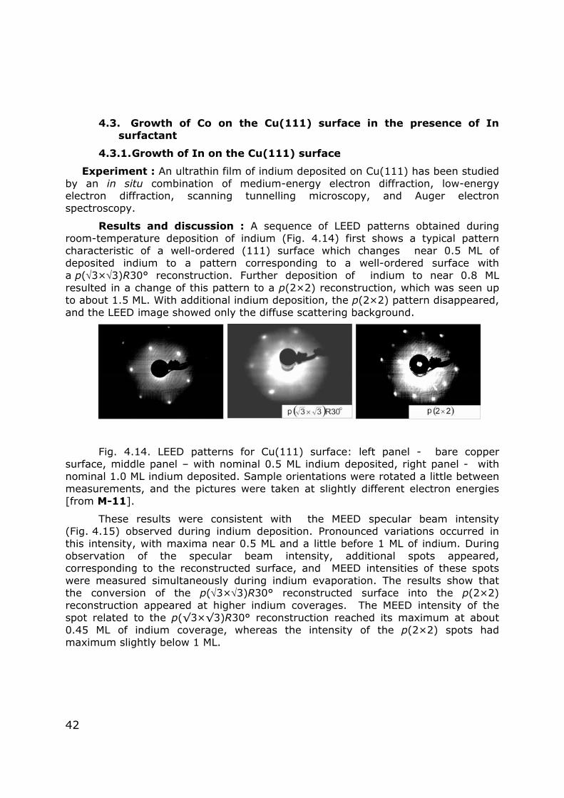
42
4.3. Growth of Co on the Cu(111) surface in the presence of In surfactant
4.3.1. Growth of In on the Cu(111) surface
Experiment : An ultrathin film of indium deposited on Cu(111) has been studied by an in situ combination of medium-energy electron diffraction, low-energy electron diffraction, scanning tunnelling microscopy, and Auger electron spectroscopy.
Results and discussion : A sequence of LEED patterns obtained during room-temperature deposition of indium (Fig. 4.14) first shows a typical pattern characteristic of a well-ordered (111) surface which changes near 0.5 ML of deposited indium to a pattern corresponding to a well-ordered surface with a p(√3×√3)R30° reconstruction. Further deposition of indium to near 0.8 ML resulted in a change of this pattern to a p(2×2) reconstruction, which was seen up to about 1.5 ML. With additional indium deposition, the p(2×2) pattern disappeared, and the LEED image showed only the diffuse scattering background.
Fig. 4.14. LEED patterns for Cu(111) surface: left panel - bare copper surface, middle panel – with nominal 0.5 ML indium deposited, right panel - with nominal 1.0 ML indium deposited. Sample orientations were rotated a little between measurements, and the pictures were taken at slightly different electron energies [from M-11].
These results were consistent with the MEED specular beam intensity (Fig. 4.15) observed during indium deposition. Pronounced variations occurred in this intensity, with maxima near 0.5 ML and a little before 1 ML of indium. During observation of the specular beam intensity, additional spots appeared, corresponding to the reconstructed surface, and MEED intensities of these spots were measured simultaneously during indium evaporation. The results show that the conversion of the p(√3×√3)R30° reconstructed surface into the p(2×2) reconstruction appeared at higher indium coverages. The MEED intensity of the spot related to the p(√3×√3)R30° reconstruction reached its maximum at about 0.45 ML of indium coverage, whereas the intensity of the p(2×2) spots had maximum slightly below 1 ML.

43
0 1 2 3
50
100
150
200
ME
ED
-Inte
nsiy
[arb
.u.]
nominal In-coverage [ML]
p(2x2)
mirror reflex
background
p(√3x√3)
Fig. 4.15. MEED intensities: marked specular intensity during evaporation of indium onto Cu(111) (mirror reflection), p(√3×√3)R30° superstructure reflection intensity (intensity beyond the dip at 0.8 ML is at background), p(2×2) superstructure reflection intensity (intensity before 0.7 ML is at background) [from M-11].
Detailed discussion of these results together with measurements of the lattice constant expansion, AES peak-to-peak intensities, and STM images of the surface development at successive stages of indium deposition is given in paper M-11. These results are interpreted as the formation of new metastable intermetallic phases, Cu2In and Cu3In, created in the deposition of indium on the Cu(111) surface.
We have observed the formation of two surface alloys by deposition of indium on Cu(111): Cu2In and Cu3In. Indium enters the Cu(111) surface substitutionally, and with more indium deposition there is copper-indium interdiffusion in the first few layers. Indium seems to prefer to be surrounded by copper, as is seen in both alloy structures (Fig. 4.16) and seems to trap other indium atoms weakly in the second neighbour position [Kla89, CDW95, Bre94, Bre92, Bre92a, Bre93].
Fig. 4.16. Schematic representation of (a) the p(√3×√3)R30° and (b) the p(2×2) real space structures [from M-11].
The difference of atomic radii of the two system components favours the creation of surface alloys with a surplus of copper because indium’s larger size forces exchanges between atoms that will lead to a smaller lattice expansion. There is no obvious transition path from Cu2In to Cu3In with increasing indium deposition. Rather, the data suggest that Cu2In reaches its maximum coverage, and then more

44
indium deposition favours diffusion of indium atoms into deeper layers (or equivalently, diffusion of copper up through the deposited indium). With initial deposition of indium, Cu2In begins to form in the surface layer, with approximately full coverage at 0.4-0.5 ML indium. Then, additional indium first piles up briefly while copper diffuses upwards to form Cu3In. Cu3In forms in the first several layers, and only with the addition of more than 3-4 ML indium is a pure indium surface coverage achieved.
4.3.2. Growth of Co on In predeposited on the Cu(111) surface
Experiment : Cobalt layer growth on Cu(111) was investigated as a function of an intermediate indium layer by an in situ combination of medium energy electron diffraction (MEED), scanning tunneling microscopy (STM), and Auger electron spectroscopy (AES).
Results and measurement : The morphology of growth and the nucleation behavior were examined. The evolution of the MEED intensities at several points in the extended reflection spots measured simultaneously during cobalt evaporation (Fig. 4.17), showed oscillations, indicative of layer-by-layer growth.
Fig. 4.17. MEED intensities at selected points in the reflection spots (where MEED oscillations were observed) for 0.66 ML, 1 ML and 3 ML pre-deposited indium [from M-12].
0 200 400 600 800 1000
-0.005
0.000
0.005
0 2 4 6 8 10
In
Co
Cu
Inte
nsity
[a.u
.]
energy [eV]
ptp
[a.u
.]
Co coverage [ML]
CoLMMCuLMM
InMNN
Fig. 4.18. Auger spectra with 0.5 ML pre-deposited indium before (upper curve) and after (lower curve) deposition of 12 ML-Co. Peak-to-peak intensities measured during deposition of cobalt on a sample with 0.1 ML pre-deposited indium for cobalt 716 eV, indium 404 eV, and copper 920 eV Auger electrons (right panel) [from M-12].
0 5 10 15 20 25
1.0
1.5
1 ML In
3 ML In
0.66 ML In
Inte
nsity
[a.u
.]
Co coverage [ML]

45
AES measurements shown in Fig. 4.18 as a function of cobalt coverage with 0.5 ML pre-deposited indium indicate that indium, but not copper, is still visible even after depositing cobalt to a coverage of 12 ML. The presence of indium on the cobalt surface was also confirmed by peak-to-peak intensity of 404 eV indium Auger electrons which decreased slowly after the first few monolayers of cobalt deposition in an approximately linear manner.
We have observed a surfactant effect of pre-deposited indium that facilitates layer-by-layer growth of cobalt on Cu(111). The pre-deposited indium enters the Cu(111) surface substitutionally as Cu2In or Cu3In, depending on indium coverage. Cobalt atoms that are subsequently deposited exchange sites with indium atoms in the surface alloy and form well-defined layers, while indium segregates to the surface as more cobalt is deposited.
Fig. 4.19. Summary schematic diagram for conditions resulting in layer-by-layer growth in the presence of pre-deposited indium, 3D-growth, and an “intermediate phase” of island growth at low cobalt coverage are also observed [from M-12].
The effect of indium on the cobalt growth mode in this system is summarized schematically in Fig. 4.19, showing regions of layer-by-layer growth in the presence of pre-deposited indium, 3D-growth, and an “intermediate phase” of island growth at low cobalt coverage. This figure is consistent with our data but is not to be taken quantitatively because of inadequate information about sample-to-sample variation. Relatively low coverage of pre-deposited indium acts as a surfactant, facilitating layer-by-layer growth of cobalt on Cu(111) up to 12-24 ML-Co. After deposition of sufficient cobalt (perhaps a few tens of ML), 3D island growth was observed, as shown in the upper region of the figure. The “intermediate phase” region corresponds to an absence of MEED oscillations with non-periodic changes of spot intensity, characteristic of an island growth mode for the deposited film.
4.4. Energetic barriers in the Co-Cu system
STM images of the surface development as cobalt is deposited, both with and without the presence of indium, showed that with 0.33 ML pre-deposited indium (Fig. 4.20) cobalt forms randomly-positioned islands which grow with higher concentration and fill the surface more evenly than for cobalt surface without pre-deposited In.
The surfactant effect of indium is connected to a reduction in the cobalt surface diffusion rate (with increased energy barrier) and therefore lowered ratio of
0 1 2 3 4 5 60
30
Intermediate phase
Layer-by-layer growth
3D-growth
Co-
cove
rage
[ML]
In-coverage [ML]

46
ES barrier to surface diffusion barrier. These indium-mediated changes in energy relations increase the probability for deposited cobalt atoms to move off an island and enlarge it laterally instead of growing up (3D growth). Indium segregates to the surface by site exchange with cobalt during cobalt deposition. However, this segregation is at less than 100% efficiency, and as the cobalt thickness increases the surfactant effect diminishes until a 3D growth mode begins again.
Fig. 4.20. STM images of surface development as cobalt is deposited, without pre-deposited indium and with 0.33 ML pre-deposited indium for different cobalt coverages as indicated on the labels [figure drawn from results of M-12].
Estimation of the surface diffusion barrier Ed for Co adatoms on the Cu(111) surface can be based on the island density. This increases with increasing deposition rate and decreasing diffusivity on the surface. Island density N depends on the size I of the critical nucleus, defined as the island size at a given temperature that becomes stable upon capture of one extra adatom. Classical nucleation theory based on a rate-equation approach predicts the island density N before island coalescence as [Ven84]:
⎟⎟⎠
⎞⎜⎜⎝
⎛++
⎟⎟⎠
⎞⎜⎜⎝
⎛≈
+
kTiiEEFN di
ii
)2(exp
2
0ν,
where F is the deposition rate, I the number of atoms of the critical nucleus, Ei the binding energy of the atoms within the critical nucleus, Ed the surface diffusion energy barrier, and T the substrate temperature. Since we did not measured any temperature dependence it is only possible to determine the change of the diffusion energy barrier from the ratio of Co island density on clean Cu(111) surfaces to the island density on In precovered Cu(111) surfaces.
For the same total amount of deposited cobalt, the smaller island size on the Cu2In surface is accompanied by increased island density. On the pure copper surface we found 380(55) islands/(100nm)2, while on the Cu2In surface we found 880(65) islands/(100nm)2. There are two possible interpretations of this higher island density: decreased cobalt diffusion or stress-limited island sizes due to the large size mismatch for cobalt on the Cu2In surface alloy. However, the second mechanism would result in more vertical growth, i.e. piling up of cobalt on the islands, while diffusion-limited islands would be both small diameter and lower in

47
height. Our STM observations are consistent only with the diffusion-limited scenario. Therefore, we conclude that cobalt diffusion is inhibited by the pre-deposited indium, and it is possible to deduce the increase of the diffusion energy barrier using Venables’s rate equation model for the kinetics [Ven87, Ven94]. Here we make the reasonable assumptions that the critical cluster size is a dimer and that the evaporation parameters and diffusivity prefactor, D0, are the same for the two deposition surfaces. Then from the ratio of the island densities we find that pre-deposited indium increases the activation energy for cobalt surface diffusion by about 0.06 eV. Prieto et al. found a surface diffusion barrier of 0.19 eV for cobalt atoms on Cu(111) [Pri00a]. So the presence of indium increases the activation energy for cobalt surface diffusion to approximately 0.25 eV.
Fig. 4.21. SFM image of 500x500 nm2 of the surface of : a) [CoCuIn]20, b) [CoCuInCoCu]10, c) [CoCu]20 from M-9].
The size of islands on [Co/Cu]20 multilayer surface prepared with and without pre-deposited indium was estimated from AFM images presented in Fig. 4.21 , and as for heteroepitaxial growth of Co on Cu(111), the island density for surfactant mediated multilayers is more than 2 orders of magnitude larger than for growth of pure Co-Cu system. Using the theory based on a rate-equation approach the activation energy for cobalt surface diffusion estimated from the island size which corresponds to the observed island density increased in the presence of a surfactant by about 0.05 eV. Although obtained at conditions different from the usual conditions of epitaxial growth, this result is in a very good agreement with the values obtained for In mediated growth of Co on Cu(111).

48
5. Summary and perspectives
The most important results of the attached papers:
1. Determination of the growth type in polycrystalline Co/Cu layers grown on Si(100) substrate and the experimental confirmation of the difference between growth of Co on Cu and Cu on Co.
2. Modification of structure and magnetotransport properties of Co/Cu multilayers by using buffer layers of different metals (noble metals vs. surfactant metals) resulted in significant increase of the GMR effect for multilayers deposited on surfactant buffers with simultaneous loss of multilayer periodicity.
3. Systematic studies of buffer layers of Pb and In surfactant metals showed different types of growth. A smoother interface was obtained for indium than for a lead buffer. The data were well described by scaling laws but the values of the scaling exponents differed substantially from the theoretical predictions of growth theories, indicating that the description of experimental growth of such systems may require additional mechanisms beyond the KPZ equation.
4. Surface morphology of [Co/Cu] multilayers deposited on Pb and In buffers is well described by scaling laws. However, the values of the scaling exponents differ much from the theoretical predictions of the nonlinear equation. Due to the observed film morphologies and scaling parameter values we cannot exclude that in the early stages of film growth the Ehrlich-Schwoebel barrier plays a significant role, but this is not the only mechanism governing the surface roughening process. Structural analysis of [Co/Cu] multilayers deposited on Pb and In buffers indicated that the buffers have broken the superlattice periodicity, inducing relatively large roughness of Co/Cu interfaces weakly dependent on buffer thickness. This effect was accompanied by the continuous rise of island size leading to the growth of system with a large flat terraces. The significant segregation of Pb to the multilayer surfaces of has been observed, indicating that Co/Cu multilayers lost their layered character and became a kind of intermediate cluster-like phase combined with a layered area. However, the influence on the magnetoresistance was advantageous – an increase of GMR value was observed for Co/Cu multilayers deposited on a Pb buffer in comparison to the system deposited on glass.
5. Systematic studies of the structure of Co/Cu multilayers with In deposited at the bilayer interface showed that indium smoothes the interfaces between Co and Cu, leading to the creation of flat interfaces and films with homogeneous thicknesses. In contrast, the roughness of pure Co/Cu multilayer interfaces is significantly greater, and the periodicity of the bilayer stack is not well conserved. The presence of indium on the surface of subsequently deposited films indicates that indium tends to segregate to the surface during deposition. This segregation appears beneficial since it maintains a high concentration of In on the surface. A high In surface
49
concentration and a high In surface mobility increase the possibility of In attachment to step edges, and reduce the Ehrlich-Schwoebel barrier, facilitating diffusion of deposited atoms. This has the effect of supressing island growth and results in flat films and smooth interfaces. The magnetoresistance ratio of Co/Cu multilayers prepared with In increased about a factor of two, but this result does not fully reflect the significant improvement of film quality.
6. Studies of low energy Auger electron from Pb and Bi surfactants at the interface of [Co/Cu] multilayers showed that concentration of surfactants measured at each stage of deposition initially increased with the number of deposited layers up to a coverage of about 15 nm at which point the surfactant concentration saturated. The experiments done on samples with different number of layer repetition confirmed the reproducibility of the segregation processes. It is seen that the segregation effect is a little stronger for Pb as compared to Bi. These results show that the surfactant already segregates to the surface of Co/Cu multilayers during the deposition process. Additional surfactants induced the creation of well-ordered structures with roughness of the order of a few Å and interfaces smoother than in the case of pure Co/Cu samples. A high degree of conformality and interface roughness replication in the surfactant mediated Co/Cu multilayers was observed. The correlated vertical roughness σc estimated from the ratio of the integrated specular and diffuse components of x-ray spectra was smaller for reference Co/Cu than for surfactant assisted Co/Cu multilayers.
7. Studies of Co/Cu multilayers with Bi and Pb surfactants deposited at the bilayer interface demonstrated that the use of surfactants in growth smoothes the interfaces between Co and Cu, and increases the layer-to-layer correlation, leading to the creation of flatter interfaces and films with homogeneous thicknesses. In contrast, the roughness of pure Co/Cu multilayer interfaces is significantly larger, and the periodicity of the bilayer stack is not well conserved.
8. The formation of two surface alloys by deposition of indium on Cu(111): Cu2In and Cu3In has been observed. Indium enters the Cu(111) surface substitutionally, and with more indium deposition there is copper-indium interdiffusion in the first few layers. Indium seems to prefer to be surrounded by copper, as is seen in both alloy structures and seems to trap other indiums weakly in the second neighbour position.
9. A surfactant effect of pre-deposited indium facilitates layer-by-layer growth of cobalt on Cu(111). The pre-deposited indium enters the Cu(111) surface substitutionally as Cu2In or Cu3In, depending on indium coverage. Cobalt atoms that are subsequently deposited exchange sites with indium atoms in the surface alloy and form well-defined layers, while indium segregates to the surface as more cobalt is deposited.
10. The effect of indium on the cobalt growth mode resulted in a qualitative phase diagram, showing regions of layer-by-layer growth in the presence of pre-deposited indium, 3D-growth, and an “intermediate phase” of island growth at low cobalt coverage. This diagram is drawn from experimental data
50
but is not to be taken quantitatively because of inadequate information about sample-to-sample variation.
11. The surfactant effect of indium is connected to a reduction in the cobalt surface diffusion rate (with increased energy barrier) and therefore a lowered ratio of the ES barrier to the surface diffusion barrier. It was found that cobalt diffusion is inhibited by the pre-deposited indium, which increases the activation energy for cobalt surface diffusion by about 0.06 eV.
12. A similar result was obtained for [Co/Cu] multilayers deposited with In at interface. The activation energy for cobalt surface diffusion increased in the presence of the surfactant by about 0.05 eV. Although this result was obtained at conditions different from the usual conditions for epitaxial growth, a very good agreement with the values obtained for In-mediated growth of Co on Cu(111) is seen.
Finally, the increase of the surface diffusion barrier entails a decreased influence of the Ehrlich-Schwoebel (ES) barrier that inhibits atoms moving over an edge from one terrace to a lower one. (This is simply due to the fact that the step-diffusion energy barrier is just the sum of the surface diffusion barrier and the ES barrier, and assuming that the effects of indium are not localized in steps.) The ES barrier is an important factor in driving 3D vs. 2D growth, because with the ES barrier being relatively high compared to the surface diffusion barrier atoms have difficulty moving over edges to extend a terrace into a smooth layer. Both smaller average island size, which increases the attempt frequency for leaving an island surface, and increased probability for a cobalt atom to step down from an island (i.e. reduced ratio of the ES barrier to the surface diffusion barrier) cause greater mass transport between layers, thereby promoting 2D-growth.
It has been shown that the deposition of low levels of certain metals remarkably affect the film composition and structure. The similar effect was also observed for non metallic additives . While the surfactants used in this work are chemically quite different the common result of their application is the significant improvement of the multilayer structure and transport properties. Understanding the mechanism by which surfactant influence the film growth is important because it may provide a new route to control thin film deposition processes and enable better atomic engineering of film structure and resulting physical properties. However, the mechanisms by which metal atoms and non metallic additives control film growth can be quite different due to their chemical properties. Our increased understanding of the factors that control atomic diffusion opens up the possibility to develop novel procedures to achieve the desired degree of perfection in polycrystalline and epitaxial multilayers, and therefore further studies in this field are desired.
51
References: [Arm98] P. Armour, C.M. Emmerson, T.-H. Shen , S.D. Evans, B.D. Rainford,
Thin Solid Films 318, 172 (1998).
[Bai88] N.M.Baibich, J. M. Broto, A. Fert, F. Nguyen Van Dau, F. Petroff, P. Eitenne, G. Creuset, A. Friederich, and J. Chazelas, Phys.Rev.Lett. 61, 2472 (1988).
[Bar05] Johannes V. Barth, Giovanni Costantini, Klaus Kern, Nature 437, 671 (2005).
[Bar95] A.–L. Barabasi and H. Stanley, Fractal Concepts in Surface Growth, Cambridge University Press, Cambridge, England, 1995.
[Bau58] E. Bauer, Z. Kristallogr. 110, 372 (1958).
[Ber96] E. Bertel and N. Memmel, Appl. Phys. A 63, 523 (1996).
[Bin82a] G. Binnig, H. Rohrer, C. Gerber, and E. Weibel, Appl. Phys. Lett. 40, 178 (1982).
[Bin82b] G. Binnig, H. Rohrer, C. Gerber, and E.Weibel, Phys. Rev. Lett. 49, 57 (1982).
[Bin86] G. Binnig, C. F. Quate, C. Gerber, Phys. Rev. Lett. 56, 930 (1986).
[Bin89] G. Binash, P. grunberg, F. Saurenbach and W. Zinn, Phys. Rev. B 39, 4828 (1989).
[Bod07] M. Bode, M. Heide, K. von Bergmann, P. Ferriani, S. Heinze, G. Bihlmayer, A. Kubetzka, O. Pietzsch, S. Blügel, R. Wiesendanger, Nature 447, 190 (2007).
[Bre92] M. Breeman and D. O. Boerma, Phys. Rev. B 46, 1703 (1992).
[Bre92a] M. Breeman, G. Dorenbos, and D. O. Boerma Nucl.Instr. and Meth. B 64, 64 (1992).
[Bre93] M. Breeman and D. O. Boerma, Surf. Sci. 287/288, 881 (1993). [Bre94] M. Breeman, G. T. Barkema, and D. O. Boerma, Phys. Rev. B 49, 4871
(1994).
[Bro63] W. F. Brown, Phys. Rev. 130, 1677 (1963).
[Cam94] J. Camarero, L. Spendeler, G. Schmidt, K. Heinz, J. J. de Miguel, and R. Miranda, Phys. Rev. Lett. 73, 2448 (1994).
[Cam96] J. Camarero, T. Graf, J. J. de Miguel, and R. Miranda, W. Kuch, M. Zharnikov, A. Dittschar, C. M. Schneider, and J. Kirschner, Phys. Rev. Lett. 76, 4428 (1996).
[Cam98] J. Camarero, J. Ferron, V. Cros, L. Gomez, A. Vázquez de Parga, J. M. Gallego, J. E. Prieto, J. J. de Miguel, and R. Miranda, Phys. Rev. Lett. 81, 850 (1998).

52
[Cam99] J. Camarero, V.Cros, M.J. Capitan, J. Alvarez, S. Ferrer, M.A. Nino, J.E.
Prieto, L.Gomez, J. Ferron, A.L. Vazquez de Parga, J.M. Gallego, J.J. de Miguel, R. Miranda, Appl. Phys. A 69, 553 (1999).
[CDW95] C. DeW Van Siclen, Phys. Rev. B 51, 7796 (1995).
[Che91] J. Chevier, V. Le Thanh, R. Buys and J. Derrien, Europhys. Lett. 16, 737 (1991).
[Cho00] H. D. Chopra, E. J. Repetski, H. J. Brown, P. J. Chen, L. J. Swartzendruber, and W. F. Egelhoff, Jr., Acta Mater. 48, 3501 (2000).
[Cho69] K. L. Chopra, Thin film phenomena. McGraw-Hill Book Company, 1969.
[Cho97] H. D. Chopra, B. J. Hockey, P. J. Chen, W. F. Egelhoff, Jr., M. Wuttig, and S. Z. Hua, Phys. Rev. B 55, 8390 (1997).
[Coe96] R. Coehoorn, J. Magn. Magn. Mater. 159, 551 (1996).
[Cop89] M. Copel, M. C. Reuter, E. Kraxiras, and R. M. Tromp, Phys. Rev. Lett. 63, 632 (1989).
[dBo95] D. K. G. de Boer , A. J. G Leenaers and W. W. van den Hoogenhof, Phil. Res. Mat. Ana. 3, 5 (1995).
[Die91] B. Dieny, V. S. Speriosu, S. S. P. Parkin, B. A. Gurney, D. R. Wilhoit, and D. Mauri, Phys. Rev. B 43, 1297 (1991).
[Ege96] W. F. Egelhoff, Jr., P. J. Chen, C. J. Powell, M. D. Stiles, and R. D. McMichael, J. Appl. Phys. 79, 2491 (1996).
[Ege96a] W.F. Egelhoff, Jr., P.J. Chen, C.J. Powell, M.D. Stiles, R.D. McMichael, C.L. Lin, J.M. Sivertsen, J.H. Judy, K. Takano, A. E. Berkowitz, J. Appl. Phys. 80, 5183 (1996).
[Ege97] W. F. Egelhoff, Jr., P. J. Chen, C. J. Powell, M. D. Stiles, R. D. McMichael, J. H. Judy, K. Takano, and A. E. Berkowitz, J. Appl. Phys. 82, 6142 (1997).
[Ehr66] G. Ehrlich, F. G. Hudda, J. Chem. Phys. 44, 1039 (1966).
[Emm96] C. M. Emmerson, T.-H. Shen, J. Magn. Magn. Mat. 156, 15 (1996).
[Ern94] H.-J. Ernst, F. Fabre, R. Folkerts and J. Lapujoulade, Phys. Rev. Lett. 72, 112 (1994).
[Fam85] F. Family and T. Vicsek, J. Phys. A: Math. Gen. 18, L75 (1985).
[Fam86] F. Family, J. Phys. A 19, L441 (1986) ; F. Family and T. Vicsek, J. Phys. A 18, L75 (1985); M. Kardar, G. Parisi, Y.-C. Zhang, Phys. Rev. Lett. 56, 889 (1986); M. Kardar, J. O. Indekeu, Phys. Rev. Lett. 65, 662 (1990).
[Fer00] J. Ferron, L. Gomez, J. M. Gallego, J. Camarero, J. E. Prieto, V. Cros, A.L. Vazquez de Parga, J.J. de Miguel, R.,Miranda, Surf. Sci. 459, 135 (2000).

53
[Fill98] Filleböck Georg, „Selbstorganisierte Nanostrukturen. Diffusion und Agglomeration von Adatomen auf der anisotropen Pd(110)-Oberfläche“, PhD thesis, Universität Konstanz, 1998.
[Ful00] E. E. Fullerton, D. T. Margulies, M. E. Schabes, M. Carey, G. Gurney, A. Moser, M. Best, G. Zelter, K. Rubin, H. Rosen and M. Doerner, Appl. Phys. Lett. 77, 3806 (2000).
[Gay84] J. G. Gay, J. R. Smith, R. Richter, F. J. Arlinghaus, and R. H. Wagoner, J. Vac. Sci. Technol. A 2, 931 (1984).; L. Z. Mezey and J. Giber, Jpn. J. Appl. Phys.21, 15 (1982).
[Gru86] P.Grünberg, R. Schreiber, Y. Pang, M. B. Brodsky und H. Sowers, Phys.Rev. Lett. 57, 2442 (1986).
[He92] Y.-L. He, H.-N. Yang, T.-M. Lu and G.-C. Wang, Phys. Rev. Lett. 69, 3770 (1992).
[Hor91] M. Horn von Hoegen, F. K. Legoues, M. Copel, M. C. Reuter, Phys. Rev. Lett. 67, 1130 (1991).
[Hor93] M. Horn von Hoegen, M. Pook, A. Al Falou, B. H. Muller, and M. Henzler, Surf. Sci. 284, 53 (1993).
[Hor94] M. Horn von Hoegen, B. H. Muller, A. Al Falou, and M. Henzler, Phys. Rev. Lett. 71, 3170 (1994).
[Hua93] T. C. Huang R. Gilles and G. Will, Thin Solid Films 230, 99 (1993).
[Hum89] C. Humphreys, Nature 341, 689 (1989).
[Inf07] http://www.infoworld.com/article/05/04/04/HN1tbdesktopdrives_1.html
[Iwa91] S. Iwanari and K. Takayanagi, Jpn. J. Appl. Phys. 130, L1978 (1991).
[Jab02] A. Jabłoński, C.J. Powell, Surface Science Report, 47, 33 (2002).
[Jaw99] J. Jaworski, M. Marszałek, J. Prokop, Z. Stachura, V. Voznyi, B. Cleff, Proc. Of Polish Vacuum Society Congress, Cracow, Poland, 25-30 May (1998), p. 141.
[Jen91] M. H. Jensen and I. Procaccia J. Physique 1, 1139 (1991).
[Jim93] M. Jimbo, T. Kanda, S. Goto, S. Tsunashima, S. Uchiyama, J. Magn. Magn. Mat. 126 422 (1993).
[Kal93] K. Kalki, M. Schick, G. Ceballos, and K. Wandelt, Thin Solid Films 228, 36 (1993).
[Kam05] M. Kamiko, H. Mizunoa, H. Chihayaa, J. Xub, I. Kojimab, R. Yamamoto, Solid State Communications 134, 803 (2005).
[Kar86] M. Kardar, G. Parisi and Y.-C. Zhang, Phys. Rev. Lett. 56, 889 (1986).
[Kla89] T. Klas, R. Fink, G. Krausch, R. Platzer, J. Voigt, R. Wesche, and G. Schatz, Surf. Sci. 216, 270 (1989).
[Koh93] M. Kohyama, R. Yamamoto, Bimonthly J. Inst. Indust. Sci.,Univ. Tokyo 45, 723 (1993).

54
[Kuch98] W. Kuch, A.C. Marley, S.S.P. Parkin, J. Appl. Phys. 83, 4709 (1998).
[Lar03] D. J. Larson, A. K. Petford-Long, A. Cerezo, S. P. Bozeman, A. Morrone, Y. Q. Ma, A. Georgalakis, and P. H. Clifton, Phys. Rev. B 67, 144420 (2003).
[Lek96] J. Lekki, M. Lekka, H. Romano, B. Cleff, Z. Stachura, Acta Physica Polonica A 89 (1996).
[Lek96a] Janusz Lekki, “Scanning Force Microscopy Studies of Implanted Silicon”, PhD thesis, Kraków 1996.
[Lev95] P.M. Levy, J. Magn. Magn. Mater. 140-144, 485 (1995).
[Li94] D. Li, M. Freitag, J. Pearson, Z. Q. Qui, and S. D. Bader, J. Appl. Phys. 76, 6425 (1994).
[Lut01] H. Lüth, Solid Surfaces, Interfaces and Thin Films, Berlin, Springer, 2001.
[Mar05] K.Marszałek, S. Kray, M.Marszałek, Zeszyty Naukowe Politechniki Warszawskiej 153, 121 (2005).
[Mar99] C. H. Marrows, N. Wiser, B. J. Hickey, T. P. A. Hase, B. K. Tanner, J. Phys.:Condens. Matter 11, 81 (1999).
[Mar99a] M. Marszałek, J. Jaworski, J. Prokop, Zb. Stachura, V. Voznyi, B. Sulkio-Cleff, Prace Naukowe Politechniki Warszawskiej, Elektronika 123, 191 (1999).
[Mey96] J. A. Meyer, H. A. van der Vegt, J. Vrijmoeth, E. Vlieg, R. J. Behm, Surf. Sci. 355, L375 (1996).
[Mod94] A.R. Modak, D.J. Smith, S.S.P. Parkin, Phys. Rev. B 50, 4232 (1994).
[Moo96] J. S. Moodera, L. R. Kinder, T. M. Wong, and R. Meservey, J. Appl. Phys. 79, 4724 (1996).
[Nak94] R. Nakatani, K. Hoshino, S. Noguchi, Y. Sugita, Jpn. J. Appl. Phys. 33, 133 (1994).
[Nee49] L. Neel, Ann. Geophys. 5, 99 (1949); Compt. Rend. Acad. Sci. 228, 664 (1949).
[Noy57] T. Noyes, W. E. Dickinson, IBM Journal of Research and Development 1, 72 (1957).
[Ost92] H. J. Osten, J. Klatt, G. Lippert, E. Bugiel, and S. Hinrich, Appl. Phys. Lett. 60, 2522 (1992).
[Pac96] G. Pacchioni, N. Rosch, J. Chem. Phys. 104, 7329 (1996).
[Par54] L. G. Parratt, Phys. Rev. 95, 359 (1954).
[Par91] S.S. Parkin, Z.G. Li, D.J. Smith, Appl. Phys. Lett. 58, 2710 (1991).
[Par91a] S.S.P.Parkin, R.Bhadra, K.P.Roche, Phys. Rev. Lett 66, 2152 (1991).
[Par95] S. S. P. Parkin, Annu. Rev. Mater. Sci. 25, 357 (1995).

55
[Per97] N. Persat, H. A. M. van der Berg, A. Dinia, J. Magn. Magn. Mat. 165, 446 (1997).
[Pet03] B. L. Peterson, R. L. White, and B. M. Clemens, Physica B 336, 145 (2003).
[Pet03a] B. L. Peterson, R. L. White, and B. M. Clemens, Physica B 336, 157 (2003).
[Poe91] B. Poelsema, R. Kunkel, N. Nagel, A. F. Becker, G. Rosenfeld, L. K. Verheij, and G. Comsa, Appl. Phys. A 53, 369 (1991).
[Pri00] J.E. Prieto, Ch. Rath, K. Heinz, R. Miranda, Surf. Sci. 454–456, 736 (2000).
[Pri00] J. E. Prieto, J. de la Figuera, R. Miranda, Phys. Rev. B 62, 2126(2000).
[Pri95] G. Prinz, Physics Today 48, 58 (1995).
[Ros93] G. Rosenfeld, R. Servaty, C. Telchert, B. Poelsema, and G. Comsa, Phys. Rev. Lett. 71, 895 (1993).
[Sav02] D. E. Savage, and M. G. Lagally, Nature 416, 498 (2002).
[Sch66] R. J. Schwoebel, E. J. Shipsey, J. Appl. Phys. 37, 3682 (1966).
[Sch94] R. Schad, C.D. Potter, P. Belien, G. Verbanck, V.V. Moshchalkov, Y. Bruynseraede, Appl. Phys. Lett. 64, 3500 (1994).
[Schö92] U. Schönberger, O.K. Andersen, M. Methfessel, Acta Metall. Mater. 40, S1 (1992).
[Sea90] In : Practical surface analysis. Vol. 1 : Auger and X-ray photoelectron spectroscopy, eds. D. Briggs and M. P. Seah, Chichester, England, Wiley, 1990.
[She97] H.L. Shen, Q.W. Shen, J.S. Yan, D.F. Shen, S.C. Zou, J. Funct. Mater. Devices 3, 229 (1997).
[Spr04] Springer Handbook of Nanotechnology, ed. Bharat Bhushan, Spinger-Verlag, Berlin Heidelberg New York, 2004.
[Ste88] D. A. Steigerwald and W. F. Egelhoff, Jr., Phys. Rev. Lett. 60, 2558 (1988).
[Ste88a] D. A. Steigerwald, I. Jacobs, and W. F. Egelhoff, Jr., Surf. Sci. 202, 472 (1988).
[Sun98] J. R. Sun, G. H. Rao, B. G. Shen, H. K. Wong, Appl. Phys. Lett. 73, 2998 (1998).
[Tho91] J. M. C. Thornton, A. A. Williams, J. E. Macdonald, R. G. van Silfhout, J. F. van der Veen, M. Finney, and C. Norris, J. Vac. Sci. Technol. B 9, 2146 (1991).
[Tho94] C. Thompson, G. Palasantzas, Y. P. Feng, S. K. Sinha and J. Krim, Phys. Rev. B 49, 4902 (1994).

56
[Tom92] M.E. Tomlison, R.J. Pollard, D.G. Lord, P.J. Grundy, J. Magn. Magn. Mat.
111, 79 (1992).
[vdB96] H. A. M. van der Berg, W. Clemens, G. Gieres, G. Rupp, W Schelter and M. Vieth, IEEE Trans. Magn. 32, 4624 (1996).
[Veg95] H.A. van der Vegt, M. Breeman, S. Ferrer, V.H. Etgens, X. Torrells, P. Fajardo, E. Vlieg, Phys. Rev. B 51, 14806 (1995).
[Ven84] J. A. Venables, G. D. T. Spiller, and M. Handbücken, Rep. Prog. Phys. 47, 399 (1984).
[Ven87] J. A. Venables, Phys. Rev. B 36, 4153 (1987).
[Ven94] J. A. Venables, Surf. Sci. 299/300, 798 (1994).
[Vil91] J. Villain, J. Phys. I 1, 19 (1991).
[Wan98] Jun Wang, Gang Li, Ping Yang, Mingqi Cui, Xiaomung Jiang, Bing Dong and Hong Liu, Europhys. Lett.42, 283 (1998).
[Wor06] D. C. Worledge, IBM Journal of Research and Development 50, 69 (2006).
[Yam93] H. Yamamoto, Y. Motomura, T. Anno, T. Shinjo, J. Magn. Magn. Mat. 126, 437 (1993).
[Yan01] D. X. Yang, B. Shashishekar, H. D. Chopra, P. J. Chen, and W. F. Egelhoff, J. Appl. Phys. 89, 7121 (2001).
[You93] H. You, R. P. Chiarello, H.-K. Kim and K. G. Vandervoort, Phys. Rev. Lett. 70, 2900 (1993).
[Zha01] Y. Zhao, G. – Ch. Wang and T. M. Lu, Characterization of amorphous and crystalline rough surfaces: principles and applications, (Experimental methods in the physical sciences, vol. 37, Academic Press 2001).
[Zha94] Z. Zhang, M. G. Lagally, Phys. Rev. Lett. 72, 693 (1994).