the hashemite university faculty of engineering
TRANSCRIPT

The Hashemite University
Faculty of Engineering Electrical Engineering Department
(Fundamentals of Electrical Circuits Lab) Lab manual
Laboratory (110409260)
Perquisites :( 110102103 & 110406229)
Experiments:
1. Lab. Equipment Familiarization
2. Measurement on DC Circuit
3. Techniques of Circuit Analysis (I)
4. Techniques of Circuit Analysis (II)
5. The Function Generator & Oscilloscope.
6. Basic Laws on AC Circuits (I).
7. Basic Laws on AC Circuits (II).

GENERAL LABORATORY RULES AND SAFETY RULES
Be PUNCTUAL for your laboratory session.
Foods, Drinks and smoking are not allowed.
Open- toed shoes are not allowed.
The lab timetable must be strictly followed. Prior permission from the lab supervisor must be obtained if
any change is to be made.
Respect the laboratory and its other user. Noise must be kept to a minimum.
Workspace must be kept clean and tidy at all time. Points might be taken off on student / group who fail to
follow this.
Handle all apparatus with care.
All students are liable for any damage to equipment due to their own negligence.
Students are strictly PROHIBITED from taken out any items from the laboratory without permission from
the lab Supervisor.
Do not work alone.
Report any injuries to your instructor immediately.
Know where the main lab power switch is located and how to turn off the power.
In the event of a fire:
De-energize the circuit
Notify the instructor immediately (he or she may use an appropriate fire extinguisher)
Remove all fuels (such as paper), if possible
Administer first aid
Call Campus Public Safety Dept. if necessary. (Pull the fire alarm, evacuate the building and call from
outside the building, if appropriate).
Make connections to a de-energized circuit only. When in doubt, do not power-up without the instructor’s
inspection.
Do not change the circuit with the power on. This can damage the components and create a safety hazard.
Do not rely on fuses, relays, circuit breakers, interlock devices or other protective devices to protect you or
your circuit.
Turn off power to all equipment when finished.
Many electrical components are hot when functioning – be careful.
Do not bypass the protective third prong on an electrical plug. Use a properly grounded adapter when
plugging into a two-prong outlet (check the outlet for proper grounding).
Report defective equipment or components to your instructor immediately. Please do not return defective
components to the Technical Support Center. (Your instructor will tag defective equipment with the nature
of the problem along with the date).
Pay particular attention to the polarity of polarized capacitors.
If a component burns, avoid breathing the fumes. They could be toxic.
Use only one hand at a time in any high-voltage circuit – prevent putting your body in the circuit.
Avoid wearing loose or floppy clothing around moving machinery. Wear safety glasses.
Do not attempt to pull someone from a “live” circuit. Turn the power off if possible. Otherwise, remove
the person with a nonconducting object.

GRADING POLICY
The total mark for this lab is distributed as follows:
Lab Report + Prelab + Quizzes + attendance 40%
Mid-term Exam 20%
Final 40%

Laboratory Report Guidelines
Effective technical communication and documentation are essential skills for an engineer. Technical
documentation can take on different forms depending on the needs of the audience. However, some common
principles can be applied to all forms of technical documentation. Consideration of these principles is essential
to ensure effective communication of the information that the audience needs. A few guidelines will be
considered here to write effective lab reports.
The following guidelines are suggested for preparing to write:
Define the Audience and It’s Needs
Establish a Purpose for Writing
Determine the Type of Documentation to be Written
Follow an Acceptable Format
Use Proper Spelling, Grammar, and Technique
Defining the Audience The audience for your report is a professor or technical assistant. They are familiar with the lab material and
need to make an assessment of your understanding of the work completed in preparation for and during the lab
session.
Establish the Purpose The purpose of writing for this lab is to provide an opportunity to develop technical writing skills, and
demonstrate understanding of the lab material. As a student, this process of organizing and writing technical
documentation is a valuable tool. Write the type of documentation that you can keep as a reference for future
use.
Determining the Documentation Type The type of documentation written for these labs will be lab reports. Depending on the nature of the lab, these
reports can be formal reports, informal reports, or status reports.
Following the Proper Format The overall structure of the each type of report is shown below.
Formal Reports Title Page
Objectives
Introduction
Methodology/Theory
Analysis/Results
Conclusion
Attached Files (Outputs, Plots, Schematics, etc.)
Informal Reports Title Page
Introduction
Analysis/Summary
Conclusion
Attached Files (Outputs, Plots, Schematics, etc.)
Status Reports Introduction
Analysis/Summary
Attached Files (Outputs, Plots, Schematics, etc.)
A brief description of each section of the reports is provided below. Use the descriptions as an outline of what
should be included in the report.
Title Page: The title page should include, in the following order, the course number, the title of the
experiment, your name, your lab partners name, the TA or professors leading the lab section, and the date the
report was submitted.
Objectives: The abstract should be a very concise, clear, and complete summary of the experiment. Do not
include specific details or references to figures, etc. The abstract should be written after completing the lab
report, and should be written in less technological terms that can be easily read and understood by a variety of
individuals with different backgrounds.
Introduction: The introduction should discuss the purpose or objective of the lab experiment. It should also
include a brief summary of the processes or procedures used in performing the lab experiment. Related history
of the subject under investigation in the lab may also be included when appropriate. The introduction should be
relatively short.
Methodology/Theory: The section on methodology or theory should discuss the experiment performed in lab.
Theoretical development associated with design procedures should be discussed, particularly in the cases where
it influences the choices you make in completing the lab experiment. This includes the work done in prelab,
simulation, and hardware. The methodology presented should be sufficiently complete for someone reading the
report to reproduce the experiment and verify the results.
Analysis/Results: The final data collected or measured should be placed in the results section. This would
apply specifically to data or measurements associated with the purpose and design specifications of the
experiment. Diagrams, numerical data organized in tables, etc. should be placed in this section, and any
pertinent analysis (but not concluding remarks) should be included. Any intermediate results that were used to
obtain the final results of the experiment do not need to be included in the report.
Summary: The summary section is for informal and status reports only. This section is a brief combination of
the methodology/theory and analysis/results sections. One brief statement of what was done in the experiment
and another brief statement summarizing the results (along with the pertinent figures, numerical data, etc.) is
all that is necessary for the summary.
Conclusion: The conclusion should respond to the goals and objectives discussed in the introduction of the
report. A general discussion of how well the experiment did (or did not) fulfill its objectives should be
presented without getting personal. Applications using the results from the experiment, or a forecast of future
events that relate to the work done in the experiment may also be included.
Attached Files: Any supporting documents, outputs, figures, etc. that are not included directly in the report
should be placed at the end of the report.
Using Proper Spelling, Grammar, and Technique
Lab reports should be proofread for proper spelling and grammar. Use the spell check features of the word
processor, and proofread. You may also want to have someone else proofread your work.
Proper technique is essential for documenting what was accomplished in the lab and for establishing the tone of
the report. Several examples of poor technique, which should be avoided, are listed below.

The lab report is not a personal experience. Do not discuss how you feel it about the experiment. Your
grade will not be based on how interesting you found the experiment, how satisfied you were personally
with the results, or how frustrated you became when things did not work properly or in a timely manner.
The lab report should not document the procedure or specific steps followed in completing the
experiment. For example, it is not necessary to explain how a circuit was wired and how components
were placed on a breadboard, or how the equipment was plugged in and measurements were made, etc.
The only exception would be when a specific procedure required to obtain the desired result is not
intuitively obvious.
Avoid using anthropomorphisms (applying human feelings or actions to inanimate objects).
Do not talk about yourself in the third person. Document what was done without using “I,” “we,” “the
student,” etc.
Use good judgment when adding detail to your reports. Do not include unnecessary or obvious information. If
there is more than one way to do something (e.g. collecting data), then add detail that describes your choice
(e.g. what piece of equipment, or what measurement function, etc. was used in collecting the data).
Additional guidelines that should be followed are listed below.
All reports must be typed, using easy to read fonts. Clip-art images, color backgrounds and borders are
inappropriate for a technical report
Figures, schematics, plots, and equations should be labeled and numbered so that they can be referred to in
the report. Inline equations are not acceptable. Equations should be separated from the text, and centered
in the page. Plot axes should have appropriate labels that clearly identify what is being represented. When
possible, equations, schematics, figures, etc. should be placed in the body of the report near the text that
first refers to them. Only include items in the appendix if they are supplementary items or if they cannot be
easily included in the body of the report.
Data that is not presented in a graph format should be organized in tables and must be identified by
appropriate title, row/column heading, and units.
Each student must submit an individual report based on individual effort. Even though partners work
together in the laboratory, each student must submit their own report.

Experiment 1
Lab. Equipment Familiarization 1.1 Objective To introduce the Multimeter, the breadboard, the power supply, resistors and their color code.
To learn to properly use the lab instruments and the correct method of measuring electrical quantities with
each instrument.
1.2 Basic Information The Digital Multimeter [DMM]
This devise is used to measure values of electrical quantities; such as voltage, current, resistance, etc.
The DMM is easy to use, and necessary for all electronics labs.
UVoltage Measurement.
Turn on the Multimeter. Using the rotary selector switch, select the voltage function [VDC]. Select the
AUTO range mode by making a long press on the range button. Insert the positive (+) lead (normally red) in the
voltage socket and the negative (-) lead (normally black) in the common socket. Place the red probe on the
higher voltage point and the black probe on the lower voltage point. The DMM will display the voltage drop
between the probe tips.
Voltage Measurement between any two points is made in parallel with the components between those two
points. If the probes are reversed the reading will be negative of the original value. A Voltmeter has very large
internal resistance, which is considered as open circuit (O.C.) during calculations.
UCurrent Measurement.
Turn on the DMM and select the current function. Place the positive (+) probe in the current socket and
the negative (-) one in the common socket. Select AUTO range mode. Connect the tips of the probes in series
with the component through which the current is being measured. A positive reading will indicate current
direction from the positive (+) to the negative (-) probes.
Current Measurement through a component is made in series with that component. An Ammeter has
very small internal resistance, which is treated as short circuit (S.C.) during calculations. Figure 1.1 shows the
connection of the DMM as a Voltmeter and an Ammeter.
Fig.1.1: DMM Connection
Important Note: Always disconnect the probes of the DMM from the circuit before changing the selector
switch from current to voltage or vise versa. Failing to do so will damage the DMM. Switching off the meter
without disconnecting the probes is insufficient for protecting the DMM. Connecting the Multimeter in an
incorrect way, or choosing the wrong selection of switches, may result in personal injury, damage to the
Multimeter and/or the lab equipment. Observe and obey safety rules and instructions at all times. If in doubt
ask your instructor.
UResistance Measurement
The ohmmeter part of a Multimeter is basically a Voltmeter and Ammeter. A built-in voltage source is
connected across the resistor to be measured and an Ammeter measures the current flow. The resistance value is
the ratio of voltage to current flow. Resistance should never be measured while it is connected in a circuit. To
measure the resistance of a component: switch off the power from the circuit. Disconnect the component from
R1
R2E
A
V
+
-
Red
Black
Red Black
I

the circuit. Switch the Multimeter to measure resistance, and select the AUTO range mode. Touch the probe tips
to the end of the ends of the component, and read the value displayed.
The Breadboard
The breadboard is a tool for effecting connections between electronic components without the need for
soldering. It consists of groups of rows and columns of socket (called busses) connected together in a
systematic way. It enables the attachment of components such as resistors, capacitors, transistors and wiring in
a versatile manner. The breadboard consists of two main parts. The thinner one, which has two long rows of
sockets that are connected together. The larger unit consists of columns of 5 sockets that are connected
together. The figure below shows the two parts, and how the elements are connected. The leads of any
component or wire are inserted into the sockets to effect the interconnection desired. The long busses of the thin
part are used for power distribution to the various parts of the circuit under test.
Fig.1.2: The Breadboard
The Power Supply
The DC power supply is used to generate a constant voltage (CV) or a constant current (CI). That is, it
may be used as a DC voltage source or as a DC current to drive the circuit under test. The unit in the lab has
two supplies: output 1 and output 2. Both outputs are variable voltage/current supplies. The variable supplies
can be used independently to achieve positive or negative output.
Obtaining a Certain Voltage from the Variable Power Supply
1. Switch the power on and make sure the output switch is made off.
2. Reduce the current and voltage knobs to minimum.
3. Switch on the output switch. [OUTPUT ON lamp turns on]
4. Increase the current knob until the CV (constant voltage) lamp turns on.
5. Increase the voltage knob up to the desired value using the coarse and fine voltage control.
6. If the CV lamp turns off after connecting the circuit under test, make sure there are no shorts in the
circuit. Then increase the current knob until CV turns on again.
Obtaining a Certain Current from the Variable Power Supply
1. Switch the power on and make sure the output switch is made off.
2. Reduce the current and voltage knobs to minimum.
3. Switch on the output switch. [OUTPUT ON lamp turns on]
4. Short the output leads of the supply. (Notice CV lamp turns off and CC lamp turns on).
5. Increase the current knob up to the desired value.
6. If the CC lamp turns off after connecting the circuit under test, increase the voltage knob until CC turns
on again. If it does not turn on this means the circuit is open.

Resistors.
The flow of charge through any material encounters an opposing force due to collisions between the
electrons and atoms in the material. This converts electrical energy into heat, and the force encountered is
called resistance. Resistors are manufactured to a specific amount of resistance. They are used in circuits for
many purposes, such as providing voltage drops and limiting current flow. The relative size of a resistor varies
with its wattage (power) rating, since a larger size sustains higher current and heat dissipation. To identify the
value of a resistor, the color code has been devised. Four or five color bands are printed on the end of the
resistor (see Table1.1).The bands are always read from the end that has the band closest to it. The first and
second bands represent the first and second digits. The third band indicates the power of 10 multiplied by the
first two digits (i.e. the number of zeros that follow the second digit). The fourth band is the tolerance, with
which the resistor was manufactured.
To reduce the cost of manufacturing resistors, only certain Preferred Values are available commercially.
Resistors are manufactured as multiples of 10 of these preferred values. They are:
1.0 2.0 3.3 5.6 8.2
1.2 2.2 3.9 6.2 9.1
1.5 2.7 4.7 6.8
1.8 3.0 5.1 7.5
All in ohm
Resistors are manufactured in fixed wattage (power rating), mainly: 1/8, 1/4, 1/2, 1, 2 Watts, etc. This is
identified by size, or printed on the component. Note that the size of a resistor is related to its current carrying
capacity. Since large currents mean higher temperatures, a larger surface is needed for the heat to be dissipated,
hence a large resistor size resistor indicates a high power rating.
1 2 3 4
Fig. 1.3: The Color Band in the Resistor
Color Bands 1 & 2 Band 3 Band 4
Black 0 1 -
Brown 1 10 1%
Red 2 100 2%
Orange 3 1k -
Yellow 4 10k -
Green 5 100k 0.5%
Blue 6 1M 0.25%
Violet 7 - 0.1%
Gray 8 - -
White 9 - -
Gold - 0.1 5%
Silver - 0.01 10%
No color - - 20%
Table.1.1: Color Code for Resistance

1.3 Equipment
Digital Multimeter (DMM), Power Supply (PS)
1.4 Procedure
1. Use the DMM to measure the resistance of the five resistors provided.
2. Read the color code of these resistors. Tabulate your results.
3. Compare your measurements with the actual values. Do the actual values lie within tolerance? Show
your calculations.
4. Holding one probe between the thumb and forefinger of each hand, measure and record the value of
your body resistance between your hands.
5. Setup your DC PS to 3.0 volts. Measure this with your DMM.
6. Repeat step 5 for 8.0 and 6.0 volts.
7. Are the values on the display equal to the DMM reading? Why?
8. Place the resistor R = 1.5 Kon the breadboard. Setup the PS to 5.0 volts and connect it to the resistor
as shown below in Fig.1.4.
9. Measure the voltage across, and the current through the resistor. Do these values match with what you
expect theoretically? Explain.
10. How much power is this resistor dissipating
Fig.
1.4: Simple Circuit Connection
E R

RIV (2-.1)
Experiment 2
Measurements on DC Circuits
2.1 Objectives
The objective of this experiment is to analyze simple resistive circuits in DC. The circuits considered here are:
resistors in series, resistors in parallel, series- parallel combination, voltage divider, current divider, and delta
combination. This experiment will allow the experimental verification of the theoretical analysis.
2.2 Equipment and Instruments
Power Supply ( PS), Digital Multimeter ( DMM) and Breadboard
2.3 Basic Information
The theoretical analysis of the circuits under study is based on Ohm’s and Kirchhoff’s laws. The main
equations relating the electrical parameters of each circuit are presented next.
1. Ohm’s law: The voltage V ( in volts, V) across a resistor is directly proportional to the current I (in
amperes, A) flowing through it. The constant of proportionality is the resistance R (in ohms, Ω).
2. Resistors in series: (See Figure 2-1)
The current through N elements in series is the same for all of them.
NS IIII ..........21 (2-2)
The voltage across the Ith element is RiIi. The sum of the voltages across each element is equal to the
Voltage applied to the entire Series combination.
1 2
1
........N
s N i
i
V V V V V
(2-3)
Equation 2-3 is formulated from Kirchhoff’s voltage law.
The equivalent resistance of the series combination is the sum of the individual resistances.
1 2 3
1
.......N
eq N i
i
R R R R R R
(2-4)
3. Resistors in parallel: (See Figure 2-2).
The voltage across N elements is the same for all of them.
1 2 ........s NV V V V (2-5)
The current through the ith element is Vi/Ri . The sum of the currents through each element is equal to
the current provided to the entire parallel combination.
1 21
.......N
s iNi
I I I I I
(2-6)
Equation 2-6 is formulated from Kirchhoff’s current law.

The reciprocal of the equivalent resistance of the parallel combination is the sum of the reciprocal of the
individual resistances.
11 2
1 1 1 1 1.........
N
ieq N iR R R R R
(2-7)
4. Series- Parallel combination: An example of a series- parallel combination circuit is shown in Figure 2-4.
The analysis of this type of circuit is accomplished by substituting the series (or parallel) combinations by their
equivalent resistances, such that the circuit is transformed into a pure parallel (or series) circuit. Once the
electrical parameters ( voltages and / or currents ) have been determined for the equivalent resistances, the
voltages and/or currents for the individual resistors in series or parallel combinations can be obtained by using
these parameters as Vs and Is for the corresponding combination.
5. Voltage divider: From Equation 2-3. A series circuit with two resistors will divide the applied voltage Vs
in to two voltages V1 and Vo across each resistor. Notice that Vo is the output of the voltage divider (See
Figure 2-4), as it is referenced to ground. The proportion in which the input is divided is given by
2
1 2
. sout
R VV
R R
(2-8)
In order for this circuit to operate as a voltage divider, the output current Io must be zero
or very small Compared with the current through R2.
6. Current divider: (See Figure 2-5). From Equation 2-6, a parallel circuit with two resistors will divide
the applied current Is in to two currents I1 and IL through each resistor. The proportion in which the input
current Is divided is given by:
2
3
2 3
. sR II
R R
(2-9)
2.4 Procedure
This part of experiment requires assembling the resistive circuits presented in figures from 1 to 5 and measuring
data from all of them.
1. Resistors in series: Assemble the circuit in Figure 2-1 with N=3 and the components values shown in
table 2-1. Take measurements to complete the entries corresponding to the experimental values.
Fig( 2-2): Resistors in series.
Parameter 1R 2R 3R eqR sV
1RV 2RV 3RV sI
Units KΩ V mA
Theoretical 1.0 2.2 5.6 10
Experimental
%Error
Table 2-1: Resistors in series

2. Resistors in parallel: Assemble the circuit in Fig (2-3) with N=3 and the component values shown in
table 2-2. Take measurements to complete the entries corresponding to the experimental values.
Fig (2-3): Resistors in parallel.
Parameter 1R 2R 3R eqR sV
1RI 2RI 3RI
Units KΩ V mA
Theoretical 1.0 2.2 5.6 10
Experimental
%Error
Table 2-2: Resistors in parallel
3. Series-parallel combination: Assemble the circuit in figure 2-3 with the component values shown in
table 2-3. Use Vs=10V. Take measurements to complete the entries corresponding to the experimental
values. Notice that the resistor experimental values can be taken from the previous measurements in
table 2-1 and table 2-2. Measure the voltage across each resistor and use Ohm’s law (Equation 2-1) and
the resistor experimental values to determine the experimental values of IRi ,I=1,2,……4.
Fig 2-4: Series-parallel combination.
Parameter Unit Theor Exper %Error Param Unit Theor Exper %Error
1R
KΩ
1.0 1RI
mA
2R 2.2 2RI
3R 5.6 3RI
4R 8.2 4RI
caR sI
abV V Vbc V
Table 2-3: Resistors in series-parallel combination
C

4. Voltage and Current divider: Assemble the circuit in Fig 2-4 with the component values shown in
table 2-4. Take measurements to complete the entries corresponding to the experimental values.
Fig(2-5): Voltage and Current divider
Parameter 1R 2R 3R sV oV sI 1I 2I
Units KΩ V mA
Theoretical 2.2 1.5 0.75 10
Experimental
%Error
Table 2-4: Voltage and current divider
2.5 Analysis
This section is intended for the analysis and comparison of the experimental and theoretical Results. Answer all
the questions.
a. Calculate the percentage error between the measured and the theoretical data and complete all
the corresponding entries in Tables 2-1 through 2-5. The percentage error is given by:
% 100%mth
th
d derror
d
Where thd and md are the theoretical and measured data respectively.
b. From the above results, discuss the possible causes of error.
c. From the results of the series- parallel combination circuit select the true statements:
(a) 4321 RRRRS IIIII , (b) bcSab VVV , (c) 4321 RRRRs IIIII
d. In the last circuit, Figure 2-5, the resistors are connected in what we call Δ connection .Using
mesh analysis can you solve this circuit?. but we can solve this circuit in much easier way by
using another technique called delta to star transformation, by using this method find Is?

Experiment 3
Techniques of Circuit Analysis (1)
(Nodal, Mesh, Superposition)
3.1 Objectives The objective of this experiment is to analyze resistive circuits in DC, employing the node-voltage
method, the mesh-current method, superposition method. Experimental results will allow the
verification of the theoretical analysis.
3.2 Basic Information In Experiment 2 the analysis of simple circuits was carried out by Kirchhoff’s laws and Ohm’s laws.
This approach can be used for all circuits. However, for circuits with more elements and structurally
more complicated a systematic approach is preferable. The techniques of circuit analysis studied here
provide an aid in the analysis of more complex circuits.
3.3 Techniques of Circuit Analysis The purpose of circuit analysis is to determine the current in each branch can be defined as a single
path in the network, composed of one simple element and the node at each end of that element - where
the current is unknown. The formulation of b independent equations with these currents as variables is
achieved by applying Kirchhoff’s laws. In a circuit with n nodes, n -1 equations are formulated by
applying Kirchhoff’s current law (KCL) to any set of n -1 nodes and the remainder b – (n -1) equations
can be written by applying Kirchhoff’s voltage law (KVL) to that number of meshes in the circuit. In
general, ne ≤ n and be ≤ b, where ne and be are the number of essential nodes and essential branches.
Therefore, the formulation of the independent equations is achieved in terms of essential nodes and
branches. However, by introducing new variables (node voltages and mesh current), the circuit can be
described with just ne – 1 equations or just be – (ne -1) equations. A brief description of each method is
presented next.
3.3.1 Node-Voltage Method The node-voltage method permits the description of a circuit in terms of ne – 1 equations. Figure 3-1
shows a circuit suitable for the analysis with the node-voltage method. In this circuit three essential
nodes can be identified (ne 3), therefore two (ne -1) node-voltage equations describe the circuit. To
select the set of ne -1 nodes to perform the analysis, one of the essential nodes is selected as a reference
node. If there is a ground node, it is usually most convenient to select it as the reference node,
otherwise the node with the most branches is chosen. The equations are then written by applying KCL
to each non reference node expressing the branch currents in terms of the node voltages. Once the
equation system is solved and the node voltages are known, all the branch currents can be calculated.
3.3.2 Mesh-Current Method The mesh-current method permits the description of a circuit in terms of b – (ne -1) equations.
Figure 3-2 shows a circuit suitable for analysis with the mesh-current method. In this circuit five
essential nodes (ne 5) and eight essential branches (be = 8) can be identified, therefore b – (ne -1) four
mesh-current equations describe the circuit. The equations are formulated by applying KVL to each
mesh, expressing the voltages across the elements on the mesh currents. Once the equation system is
solved and the mesh currents are known, all the branch currents (and any other parameter of interest)
can be calculated.
3.3.3 Techniques of Linear Circuit Analysis The previous two techniques hold for all types of circuits in general, but there are some techniques
that can only applied to only specific circuits not for all circuits, linear circuits are one of this type of
circuits. Let us define a linear element as a passive element that has a linear voltage-current
relationship. By a “Linear voltage-current relationship” we simply mean that multiplication of current
through the element by a constant K results in the multiplication of the voltage a cross the element by
the same constant K. We must also define a linear dependent source as a dependent current or voltage
source whose output current or source is proportional only to the first power of a specified current or

voltage variable in the circuit or to the sum of such quantities. We must define also a Linear circuit as a
circuit composed entirely of independent sources, linear dependent sources, and linear elements.
The Superposition Principle
Some circuits have more than one current or voltage source. Superposition theorem defines a method to
determine the currents and voltages in such a circuit. This is done by considering each source at a time,
while all other sources are replaced by their internal resistances. The superposition theorem states:
Current (or voltage) in any given branch of a multiple-source linear circuit can be found by determining
the currents (or voltages) in a particular branch, produced by each source acting alone, with all other
sources replaced by their internal resistances. The total current (or voltage) in the branch is the algebraic
sum of the individual source currents ( or voltages) in that branch.
The steps in applying the theorem are as follows:
1. Choose one source at a time, and replace all other voltages sources with a short circuit (R=0),
and all other current sources with an open circuit(R=∞).
2. Determine the currents and voltages required.
3. Repeat steps 1 & 2 for each source in the circuit.
4. The total current or voltage in a branch is the algebraic sum of the individual source currents or
voltages in that branch.
3.4 Procedure
This part of experiment requires assembling the resistive circuits presented in the previous section and
measuring data from all of them.
1. Node-Voltage Method.
a. Assemble the circuit in Figure 3-1 with the component values shown in Table 3-1.
Figure 3-1: Simple Circuit to Apply Nodal Analysis
Parameter Unit Theoretical Experimental %Error
R1
KΩ
4.7
R2 1.5
R3 1.8
R4 3.3
R5 1.0
R6 2.2
R7 6.8
V V 10
Table 3-1: Results of the Measured Resistances

b. Measure the voltage and current across and through each resistance respectively
Parameter Unit Theoretical Experimental %Error
VAF FF
KΩ
V
VAB
VAC
VAD
VAE
VBC
VCD
VDE
I1
I2
I3
I4
I5
I6
I7
I8
mA
I9
Table 3-2: Results of Nodal Analysis
2. Mesh-Current Method.
a. Assemble the circuit in Figure 3-2 with the component values shown in Table 3-3.
Figure 3-2: Simple Circuit to Apply Mesh an Superposition Techniques
Parameter Unit Theoretical Experimental %Error
R1
KΩ
2.2
R2 3.3
R3 4.7
R4 6.8
R5 5.6
R6 8.2
V1
V
10
V2 5
Table 3-3: Results of the Measured Resistances

b. Measure the voltage and current across and through each resistance respectively.
Parameter Unit Theoretical Experimental %Error
VAD FF
KΩ
V
VDF
VBE
VEG
VCD
VBG
VFA
mA
I1
I2
I3
I4
IDC
IAD
IDF
Table 3- 4: Results of Mesh Analysis
3. Superposition.
Determine the experimental values in circuit Figure 3-2 by using superposition
a. Replace V1 with a short circuit, keep V2 ON, Take measurements to complete the entries
corresponding to the experimental values in table 3-5. Be careful to follow the passive sign
convention. b. Replace V2 with a short circuit, keep V1 ON, Take measurements to complete the entries
corresponding to the experimental values in table 3-6.
Parameter Unit Theoretical Experimental %Error
V'AD FF
KΩ
V
V'DF
V'BE
V'EG
V'CD
V'BG
V'FA
mA
I'1
I'2
I'3
I'4
I'DC
I'AD
I'DF
Table 3- 5: Results of Superposition When Removing V1

Parameter Unit Theoretical Experimental %Error
V"AD FF
KΩ
V
V"DF
V"BE
V"EG
V"CD
V"BG
V"FA
mA
I"1
I"2
I"3
I"4
I"DC
I"AD
I"DF
Table 3-6: Results of Superposition When Removing V2
3.5 Analysis
1. From your results in table 3-2, prove that KCL holds true. Write anodal equation at each node, do
the summation. For your equations, choose Current going out of the node. Each node should sum to 0.
2. From your results in table 3-4, prove that KVL holds true. Write a loop (mesh) equation for each
loop. Do summation. Each mesh should sum up to 0.
3. From your results in tables 3-4, 3-5 and 3-6, prove that superposition holds true. The summation of each
voltage and each current in table 3-5, with its corresponding in table 3-6, should be equal to the corresponding
values in table 3-4.
4. The Ammeter readings that you observe in the experiment, was a mesh current of a branch current?
Justify your answer?

Experiment 4
Techniques of Circuit Analysis (2)
(Thevnin, Norton and Maximum Power Transfer).
4.1 Objectives
The objective of this experiment is to simplify resistive circuits in DC employing the Thevenin and Norton
equivalents. Experimental results will allow the verification of the theoretical analysis. Also to verify the
maximum power transfer theorem, this will lead us to learn about some types of variable resistors such as
decade resistance box and potentiometers.
4.2 Basic Information
In experiment 2 was demonstrated the use of series-parallel reductions of resistive circuits in order to simplify
the circuit analysis. In this experiment, Thevenin and Norton equivalent circuits are discussed as additional
methods to simplify the circuit analysis.
4.2.1 Thevenin's Theorem
Any linear network may, with respect to a pair of terminals. be replaced by an equivalent
voltage source VTh ( equal to the open circuit voltage) in series with a resistance RTh seen between
these terminals. The theorem presents a very useful method for simplifying complex circuits. We must
realize that the equivalency is with respect to a selected pair of terminals. We replace the original
circuit lying on one side of a pair of terminals by its equivalent Thevenin voltage source and
resistance. To evaluate VTh and RTh follow the steps:
1. Open-circuit the terminals to which the Thevenin equivalent is desired. In other words disconnect
all of the circuitry that will not be replaced by the equivalent circuit.
2. RTh is the total resistance at the open-circuit terminals, when all voltages sources are replaced by
short circuits, and open circuits replace all current sources.
3. VTh is the voltage a cross the open-circuited terminals.
4. Replace the original circuitry by its Thevenin equivalent circuit, with the Thevenin terminals
occupying the same position as the original terminals. The external circuit removed in step 1 may
now be reconnected.
4.2.2 Norton's Theorem
Any linear network may, with respect to a pair of terminals, be replaced by a current source IN (equal
to the short- circuit current) in parallel with the resistance RTh seen between the two terminals. Similar
to Thevenin's Theorem, we are presented with a simple method of reducing a more complex circuit to
a simpler one. The difference lies in converting the reduced circuit to a current source instead of a
voltage source, with the equivalent resistance in parallel rather than in series. To evaluate IN and RN
follow the steps:
1. Follow the procedure in step 1 of Thevenin's equivalents.
2. RN =RTh calculated in step 2 above.
3. IN is the short circuit current passing through the terminals?
4. Replace the original circuitry by its Norton equivalent circuit, with the Norton terminals occupying
the same position as the original terminals. The external circuit removed in step 1 may now be
reconnected.

4.2.3 Maximum Power Transfer Theory
An independent voltage source in series with a resistance Rs, or an independent current source
in parallel with a resistance Rs, delivers maximum power to a load resistance RL when Rs = RL .
The maximum power delivered, in this case, is
2
max 4th
th
VP
R (4-1)
4.3 Procedure 1. Thevenin and Norton Equivalents:
a. Assemble the circuit in Figure 4-6 with the component values
shown in Table 4-1. (RL is 10 KΩ potentiometer (Pot), in this
section there is no need to connect this Pot. in the circuit.
Fig. 4-6: Simple Circuit to Measure Thevenin Equivalent
Parameter Unit Theoretical Experimental %Error
1R
KΩ
1.0
2R 1.5
3R 1.0
4R 3.3
5R 2.2
6R 1.0
thR
1sV
V
12
2sV 5
thV
scI mA
Table 4-1: Results of Thevenin Equivalent

b. thV Measurement:
to measure OCV , disconnect RL, and measure VAB, Where thV = OCV = ABV .
c. Isc Measurement:
to measure Isc place, A-B terminals should be Shorted by the Ammeter. (Connect the Ammeter
across A- B Terminals).
d. Rth Measurement:
to measure Rth, short sources Vs1, Vs2 and Connect the Ohmmeter across terminals A-B.
2. Maximum Power Transfer:
a. Set the pot. To 1KΩ, reconnect it in the circuit, Measure the voltage across the pot. Calculate the
power dissipated by the pot.
b. Increase the pot. Resistance in steps as illustrated in Table 4-2
c. Take measurements corresponding to the entries in the table.
Table 4-2: Results of the Measured LV and P
4.4 Analysis
1. Plot on graph paper, a graph of the power dissipated in the pot. vs. its resistance.
Indicate the point of maximum power on the graph.
2. Calculate the Thevenin's equivalent circuit that can be seen from Points A,B. Calculate MAXP .
3. Show whether the maximum power transfer theorem holds for this circuit or not.
4. Explain, in your words, the effect of load on the voltage relationships in a voltage divider circuit.
LR (KΩ) LV (V) RL
VLP
2
mW
Theor. Exper. %Error Theor. Exper. %Error Theor. Exper. %Error
0.22
0.33
2.2
1
3.3
4.7
47
100

Experiment 5
The Function Generator and Oscilloscope
5.1 Objectives:
To introduce time varying and periodic signals.
To introduce the Function Generator as lab tool
To introduce the Cathode Ray Oscilloscope as a lab tool.
5.2 Basic Information:
5.2.1 Time varying and periodic signals:
Time varying signals are signals whose values change with time f = f(t) [Fig 5.1].
t
f(t)
Fig 5.1: Varying Signal
Examples of such signals include:
- The ramp signal f(t) = t .
- The sinusoidal signal f(t) = A sin( t).
- The exponential signal f(t) = te .
An important subset of time varying signals is the set of periodic signals [Fig. 5.2], defined by the equation:
f(t)=f(t+T)
Where T is the period of the signal.
T
t
f(t) f(t)
t TT
Fig. 5.2: Set of Periodic Signals Fig. 5.3: Common Periodic Signal
A common periodic signal is the square wave [Fig 5.3], defined by the equation:
n
n
TntunTtuAtf ))](()([)( (5-1)
Where is the width, if the pulse T is the period, and u(t) is the unit step function.

5.2.2 The Sinusoidal Signals:
An important periodic signal is the sinusoidal signal.
)sin()( tAtf (5-2)
In studying this signal several important parameters can be identified. Given the signal
)2sin()sin()( ftAtAtV (5-3)
Where:
A : The amplitude of the signal, also known as the peak voltage V Bp.
: the radian frequency measured in rad / sec.
f : The frequency measured in Hz. B
VBp-p : 2A, the peak to peak voltage.
T : The period, equal to the reciprocal of the frequency.
: The phase angle of the signal.
Another important parameter of the sinusoidal signal is the RMS value, which stands for the RMS. It is
calculated by the formula:
2
AVRMS
The RMS value is defined as the effective value of the sinusoidal signal, equal to the DC signal would deliver
the same power if applied to the same resistor.
For RMS value for v is given in equation (5-4)
0
0
2 2
cos( )
1cos ( )
m
t T
rms m
t
v V t
V V t dtT
(5-4)
The RMS values for the triangle and the square wave are:
3
AVRMS , for triangle wave.
AVRMS , for square wave.
Where A is the peak voltage.
t
V(t)
A
-A
Fig. 5.4: The Sinusoidal Signal

5.2.3 The Function Generator (FG):
The function generator is an instrument that delivers a choice of different waveforms, with adjustable
frequency over a wide range. The most common waveforms are: sine, triangle and square.
The value of the current is controlled by the frequency control circuit, the constant current ids fed to an
integration circuit, the output of which is a triangular signal. A comparator uses the triangular wave to supply
a sine wave. While the sine shaping circuit converts the triangular wave into a sinusoidal signal. Through a
selector the amplifier provides the output signal.
Fig. 5.5: Front View of a FG
The following table describes the controls and indicators of the FG used in lab.
COUNTER DISPLAY Display the frequency of the internally generated waveform
RANGE switch Select output frequency range. Seven ranges from 1Hz to 10 MHz, for
example if the 100 KHz range is selected, the output frequency can be
adjusted from 10 KHz to 100 KHz.
FREQUENCY
CONTROL
Sets the desired frequency within the range selected. This is done by
setting both the CAORSE and FINE controls.
FUNCTION switch Selects Sine, Square or triangle waveform as OUTPUT jack
OUTPUT LEVEL
control
Controls the Peak-to-Peak amplitude of the signal at the output jack.
-20 dB switch For amplitude attenuation at –20 dB level.
OUTPUT jack The output signal.
TTL/CMOS jack A square (TTL/CMOS) wave and it depends on the position of the
CMOS LEVEL switch.
DC OFFSET control This control is enabled by the DC OFFSET switch.
DUTY CYCLE control Enabled by the DUTY CYCLE switch and by rotating this dial the duty
cycle of the main signal is adjusted
GATE LED Indicates when the frequency counter display is updated. When selecting
any of the RANGE switches. The LED will flash number of times
depending on the selected range. As the LED turns off , the display is
updated.
Table 5.1: Controls and Indicators
5.2.4 The Cathode Ray Oscilloscope (CRO):
The CRO displays the amplitude of the electrical signals, on screen, as a function of time. The horizontal axis
of the CRO is deflected at a constant time rate. While the vertical axis is deflected in response to the
amplitude of an input signal. The heart of the oscilloscope [ Fig. 5.6] is the cathode ray tube (CRT). The CRT
generates an electron beam, accelerates the beam to high velocity, and deflects it to create the image. The
oscilloscope has a time base generator which supplies the correct voltage to the CRT to deflect the beam ( a
spot on the screen) horizontally, at a constant time rate. The signal under study is fed to the vertical amplifier,
to increase its amplitude, and then to the CRT to deflect the beam vertically. To synchronize the horizontal
and vertical deflections, a triggering circuit is used.
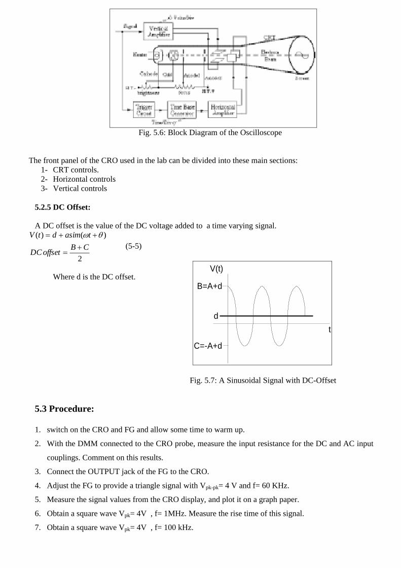
Fig. 5.6: Block Diagram of the Oscilloscope
The front panel of the CRO used in the lab can be divided into these main sections:
1- CRT controls.
2- Horizontal controls
3- Vertical controls
5.2.5 DC Offset:
A DC offset is the value of the DC voltage added to a time varying signal.
2
)()(
CBoffsetDC
tasimdtV
(5-5)
Where d is the DC offset.
5.3 Procedure:
1. switch on the CRO and FG and allow some time to warm up.
2. With the DMM connected to the CRO probe, measure the input resistance for the DC and AC input
couplings. Comment on this results.
3. Connect the OUTPUT jack of the FG to the CRO.
4. Adjust the FG to provide a triangle signal with Vpk-pk= 4 V and f= 60 KHz.
5. Measure the signal values from the CRO display, and plot it on a graph paper.
6. Obtain a square wave Vpk= 4V , f= 1MHz. Measure the rise time of this signal.
7. Obtain a square wave Vpk= 4V , f= 100 kHz.
t
V(t)
B=A+d
C=-A+d
d
Fig. 5.7: A Sinusoidal Signal with DC-Offset

8. Use dual mode to compare OUTPUT and TTL/CMOS outputs in amplitude, frequency, waveform ,
phase. Plot both signals in one graph paper using the same time scale.
9. Use the ADD function of the oscilloscope to get OUTPUT +TTL/CMOS. Set both channels to the
same volts/div scale. Plot the resulting waveform.
10. Invert CH2 and get OUTPUT -TTL/CMOS, Plot the resulting waveform.
11. Obtain a sine wave with Vpk-pk= 8 V, f = 15KHz. Press the DC OFFSET button, increase the dc
offset until the sine wave starts to be distorted.
12. Measure from the CRO the maximum value of DC offset at which an undistorted output is possible.
Set the DMM to measure a DC voltage and measure the OUTPUT jack. Compare with the CRO
results.

Experiment 6
Basic Laws onAC Circuits(I)
6.1 Objectives - To introduce time varying and periodic signals.
- To implement Ohm Law, KVL, KCL for AC circuits.
6.2 Basic information
The Voltage-Current Characteristic of a Resistor
For a resistor, the relation between current and voltage is linear. It is given by Ohm’s law:
)()( tiRtv
This relation does not change for the sinusoidal signal or any other signal. Therefore the Ohm’s law
can be expressed in the phasor form as following:
V = R I mm IRV
Clearly the voltage amplitude is merely the current amplitude multiplied by the constant R. A resistor
does not introduce phase shift between the voltage across and the current through it. Furthermore the
above relationships are independent of the frequency of the sinusoidal signal.
6.3 Equipment FG, CRO, DMM, and several of components.
6.4 Procedure 6.4.1 Part A
1. Use the FG to generate a sinusoidal with amplitude of 10Vp-p, and frequency of 1.5KHz.
2. Implement the circuit in (figure 6.1) Check the source signal after connection.
3. Use the DMM to measure the current in the circuit I(t). Don’t forget to switch the DMM to AC.
4. Observe and recorder the signal of CH1 on the CRT (oscilloscope).
5. Calculate the current in the circuit, its frequency and peak voltage across the resistor.
6. Write down the formulas for V(t), and I(t) as a function of time.
( ) sin( )mV t V t ( ) sin( )mI t I t πf
7 Plot the signal V(t) and I(t) on the same graph paper using the same time scale.
8 Calculate Irms and compare this with the value measured by the ammeter. Calculate Vrms
from the CRO display of V(t).
9 Verify that Ohm Law holds for RMS values.
10 Change the frequency of V(t) to 15KHz, repeat steps 2 till 9. Is Ohm Law frequency dependent?
Figure 6.1

6.4.2 Part B
1 Generate V(t), a sinusoidal signal with Vp = 2V, ω = 15.7Krad/s.
2 Assemble the circuit in (fig 6.2). Where R1 =1.8KΩ, R2 = 1KΩ, R3 = 750Ω. Check and adjust, if
necessary, the source signal after connection.
3 Use the CRT to display the signals V1(t), V2(t), V3(t), and draw them underneath each other on one
sheet of graph paper using the same scale.
Important note: V1(t) cant be measured by placing the CRT probes directly across R1, as this will
ground the resistors R2 and R3, invert CH2 display and add CH2 to CH1 to get CH1 – CH2 = V1(t).
4 Show that KVL applies to the time functions of voltages in this circuit.
5 Calculate the current in each one of the resistors. Dose KCL apply? Show that from your calculations.
6 Measure the RMS values of all currents and voltages in the circuit.
7 Calculate the above RMS value and compare with the measurements. Show that KVL & KCL apply
to the RMS values.
Figure 6.2

Experiment 7
Basic Laws on AC Circuits(II)
7.1 Objective 1. To introduce time varying and periodic signals.
2. To investigate the voltage-current relationship, and its dependence on frequency for resistors,
capacitors, and inductors.
3. To implement Ohm’s law, KVL and KCL for AC circuits.
7.2 Basic Information
7.2.1 The Voltage-Current Characteristic of a Capacitor
For a capacitor, the relation between current and voltage is:
dttiC
tv )(1
)(
This relation does not change for the sinusoidal signal or any other signal. For sinusoidal signals, the
phasor form is given by:
V = CJ
1I
The voltage amplitude is the current amplitude divided by the constant C and the radian frequency .
Therefore, the voltage amplitude is inversely related to the frequency. In addition the current leads the
voltage by an angle of 090 .
7.2.2 The Voltage-Current Characteristic of an Inductor
For an inductor, the relation between current and voltage is:
)()( tidt
dLtv
This relation does not change for the sinusoidal signal or any other signal. For sinusoidal signals, the
phasor form is given by:
V = Lj I
The voltage amplitude is the current amplitude multiplied by the constant L and the radian frequency
. Therefore, the voltage amplitude is directly related to the frequency. In addition, the current lags
the voltage by an angle of 090 .
7.2.3 Applaying KVL and
KVL and KCL are applicable to AC signals the same way they are for DC signals:
a- KVL: the algebraic sum of the voltages around any closed path in a circuit is zero.
00
N
i
iV
Where N is the number of drop voltages around any closed loop.
b- KCL: the algebraic sum of the currents around entering any node is zero.
00
N
i
iI
Where N is the number of entering currents through any node.
7.2.4 Measuring Current with CRO

To study the voltage-current characteristic of any component Z, it is necessary to observe both the
voltage across and the current through this component. Since CROs display voltage only, an indirect
method must be used to display current.
By placing a resistor R in series with the component Z(see figure7.1)the voltage drop across the
resistor will be directly related to the current in Z, and this voltage can be observed on the CRO. By
dividing the value of this voltage by the resistance value of R, we get a measure of the current in Z.
The resistor R must be small to limit the voltage across it, and its power rating should be considered
carefully to sustain the current in the circuit.
Figure7.1 Measuring Current with CRO.
7.2.5 Measuring Phase Shift with CRO
To measure the phase shift between two signals (see figure7.2) with the same shape and the same frequency.
Observe the following procedure:
1. Connect the two signals to the two channels of the CRO. They must both have the same ground level.
2. Choose one of the signals as the reference.
3. Measure the number of horizontal divisions for one full cycle of the reference signal ( the distance B ).
4. Measure the number of horizontal divisions between two corresponding points of the wave forms (the
distance A).
5. The phase shift is given by the formula:
Figure7.2 Measuring Phase Shift with CRO.
7.3 Equipments

FG, CRO, DMM, and various components.
7.4 Procedure
7.4.1 Part A
1. Use the FG to generate a sinusoid of 8 PKPKV at 500 Hz.
2. Implement the circuit in figure7.4. Check the source signal after assembly.
3. Observe and record the signals of CH1 and CH2. Measure the amplitude and the phase shift of the
current..
4. Plot the signals v(t) and i(t) on the same graph paper.
5. Change the frequency of v(t) to 5 KHz and repeat steps 2 till 4
Parameter Unit Calculated value Measured value % error
I (500 Hz) A
I (500 Hz) o
I (5 KHz) A
I (5 KHz) o
7.4.2 Part B
1. Use the FG to generate a sinusoid of 8 PKPKV at 500 Hz.
2. Implement the circuit in figure 7.5. Check the source signal after assembly.
3. Observe and record the signals of CH1 and CH2. Measure the amplitude and the phase shift of the
current..
4. Plot the signals v(t) and i(t) on the same graph paper.
5. Change the frequency of v(t) to 5 KHz and repeat steps 2 till 4.
Parameter Unit Calculated value Measured value % error
I (500 Hz) A
I (500 Hz) o
I (5 KHz) A
I (5 KHz) o
7.4.3 Part C
Figure 7.4: Circuit of Part B.
V(t)
R210ohm
CH1
CH2
GND
C1 1uF
Figure 7.5 :Circuit of Part C.

1. Use the FG to generate a sinusoid of 8 PKPKV at 5 KHz.
2. Measure the resistance of the inductor, add this resistance to the value of R2. Assemble the circuit in
figure 6. Check the source signal after connecting.
3. Repeat the steps 3 till 5 of part B.
Parameter Unit Calculated value Measured value % error
I (500 Hz) A
I (500 Hz) o
I (5 KHz) A
I (5 KHz) o
7.5 Calculations and Questions:
Part A:
Note: Answer questions for both frequencies 500 Hz and 5 KHz.
For the circuit shown in figure 7.4:
1. Calculate the amplitude of the current I .
2. Calculate the angle of the current I .
3. Write v(t) and i(t) as functions of time. Is there a phase shift between v(t) and i(t)?
4. Verify (using obtained results) that Ohm’s law holds in pharos form.
6. Is the relation between current and voltage in this circuit affected by changes in frequency?
Part B:
For the circuit shown in figure 7.5:
Note: Answer questions for both frequencies 500 Hz and 5 KHz.
1. Calculate the amplitude of the current I .
2. Calculate the angle of the current I .
3. Write v(t) and i(t) as functions of time. Is there a phase shift between v(t) and i(t)?
4. Verify (using obtained results) that Ohm’s law holds in phasor form.
5. Is the relation between current and voltage in this circuit affected by changes in frequency? How?
Part C:
For the circuit shown in figure 7.6:
Note: Answer questions for both frequencies 500 Hz and 5 KHz.
1. Calculate the amplitude of the current I .
2. Calculate the angle of the current I .
3. Write v(t) and i(t) as functions of time. Is there a phase shift between v(t) and i(t)?
4. Verify (using obtained results) that Ohm’s law holds in phasor form.
5. Is the relation between current and voltage in this circuit affected by changes in frequency? How?
Figure 7.6: Circuit of Part D