the gbt a single link for timing, trigger, slow control and daq in experiments a. marchioro...
TRANSCRIPT

The GBT
A single link for Timing, Trigger, Slow Control and DAQ in experiments
A. Marchioro CERN/PH-MIC

A. M. GBT2
Project Participants
CERN: PH-MIC & ED & ATE INFN: Bari, Bologna, Torino IN2P3: Marseille
A. M. GBT3
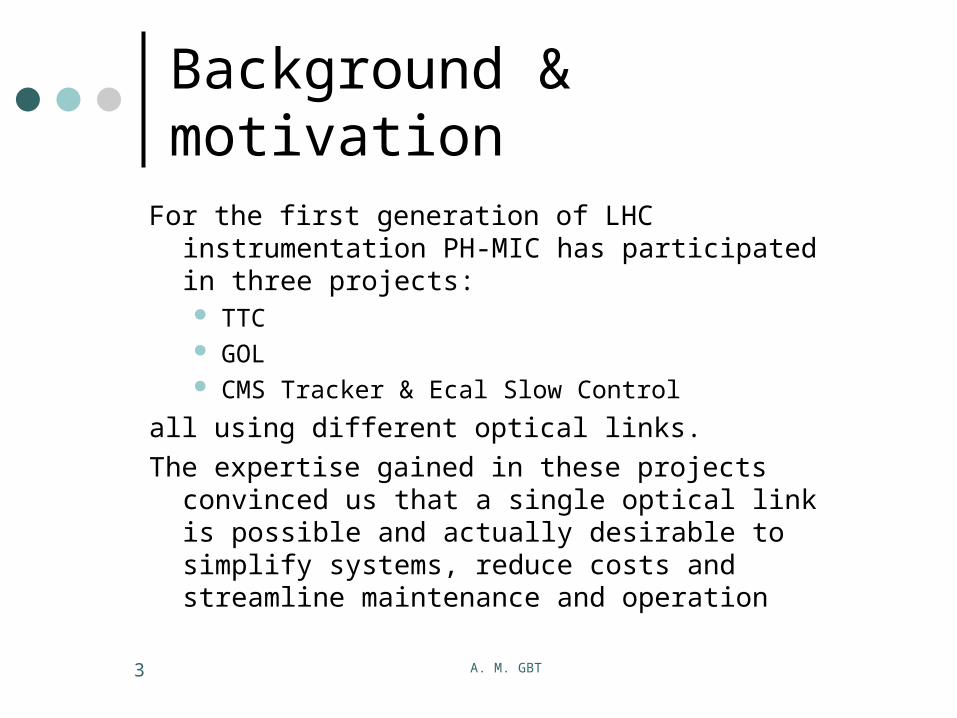
Background & motivation
For the first generation of LHC instrumentation PH-MIC has participated in three projects: TTC GOL CMS Tracker & Ecal Slow Control
all using different optical links. The expertise gained in these projects
convinced us that a single optical link is possible and actually desirable to simplify systems, reduce costs and streamline maintenance and operation

A. M. GBT4
Rationale Cost of optical transmission system is largely
dominated by the opto components (and their installation) and NOT by the electronic components
Cost changes moderately when increasing speed Therefore: increasing design cost of electronic
components has small if any impact on overall system cost but can lead to many advantages in terms of: functionality overall cost reduction compatibility with industrial standards simplification of long term maintenance reduction of number of links

A. M. GBT5
Outline
General Aim of the ProjectArchitectureProposed TTC functionality
Some details on proposed Error Correction
Proposal for interface to Slow Control Progress & Plans

A. M. GBT6
General aim
Embedded Electronics Counting Room
GBT GBT
Timing & Trigger
Slow Control
DAQ Path
Timing & Trigger
DAQ Path
Slow Control
GBT GBT
Timing & Trigger
Slow Control
DAQ Path
Timing & Trigger
DAQ Path
Slow Control

A. M. GBT7
General aim++
Embedded Electronics Counting Room
GBT
8-16channelsGBT-like
FPGA
Timing & Trigger
Slow Control
DAQ Path
Timing & Trigger
DAQ Path
Slow Control
…

A. M. GBT8
Architectural Options
… …
Straightforward P2P Architecture +Technology
PON Derived Architecture +Technology
A. M. GBT9
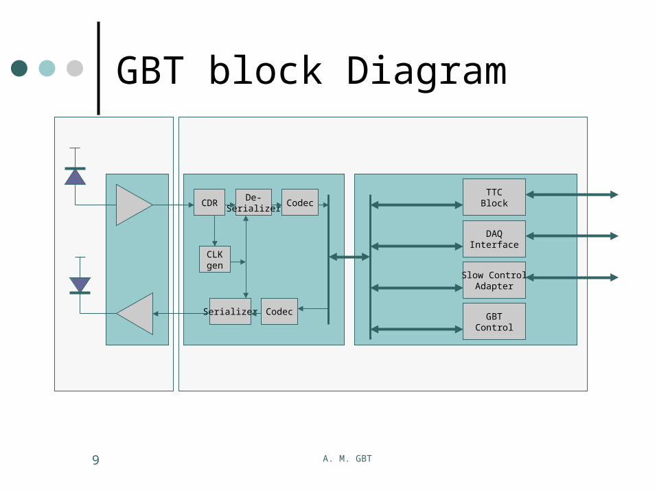
GBT block Diagram
CDRDe-
SerializerCodec
Serializer Codec
TTCBlock
DAQInterface
Slow ControlAdapter
GBTControl
CLKgen

A. M. GBT10
TTC Functionality
40 MHz clock & skew
Generator
Arbitrary 8 bit function
generator4K deep
GBT Clock
TriggerDecoder
GBT internal data bus
Clock40<3:0>
Trigger<7:0>
AuxTrigger<7:0>
If the SLHC will finally run @ 20 MHZ, a function will be provided to gate the 40 MHz in a programmable manner
Embedded GBT Counting Room GBT
TriggerEncoder
Trigger<7:0>
40 MHz clock
Generator
Serializer

Error Correction in GBT

A. M. GBT12
Objective for FEC Correct burst errors in link
Generated on the p.i.n. diode Generated by particles hitting receiving PLL
or any other circuitry causing momentary phase error
Generated in the receiver S/P register (which cannot be triplicated)
Do this with minimal latency Excludes certain FEC methods
Achieve good efficiency Merge nicely with line-coding
A. M. GBT13
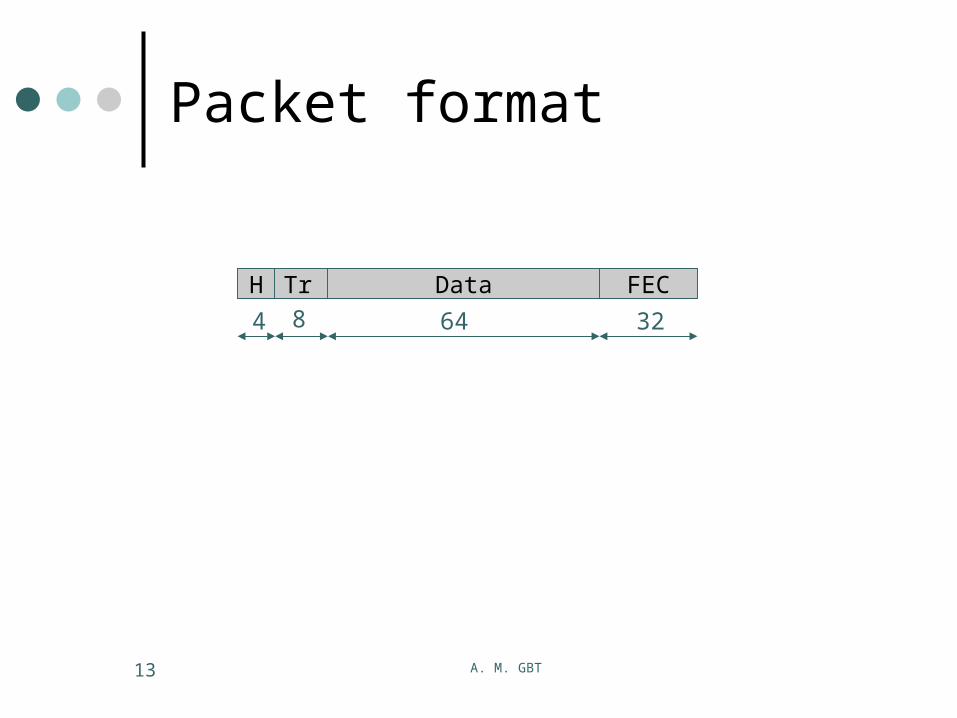
Packet format
Data FECTrH
648 324

A. M. GBT14
Coding proposed Fully FEC coded
64 data bits, 8 trigger bits -> Total user bits 72 Not coded
4 header bits -> Total 76 bits RS(15,11) with symbols of 4 bits Coding/Decoding latency: one 25 ns cycle Interleaving: 2 Error correction capability:
2Interleaving x 2RS = 4 symbols, i.e. 16 bits Total bits used: 108 (= 76 + 32) Code efficiency: 73.3% Line speed @ 40 MHz/word = 4.32 Gbit/s
Problem : does not match nicely with FPGAs, changes are likely,other similar schemes under evaluation
Interface to Slow Control

A. M. GBT16
Slow Control Architecture
GBT GBT
Timing & Trigger
Slow Control
DAQ Path
Timing & Trigger
DAQ Path
Slow Control

A. M. GBT17
Two Chips Solution
GBT GBT
Timing & Trigger
DAQ Path
Timing & Trigger
DAQ Path
Slow Control
GBTSCA
User Buses
100 Mb EthernetUser Buses:- I2C- Single-wire- Parallel bus- JTAG- Memory- Monitoring 12b ADC

A. M. GBT18
802.3-TX Interface Detail
Protocol between GBT and SCA same as between MAC and PHY Several versions
exists (only pin count changes)
• MII, RMII, SMII,…
GBT looks like the “PHY” to the slow control system It carries the
Ethernet protocol across
GBT
GBTSCA
(R/S)MII Interface

A. M. GBT19
GBT-SCA
802.3MAC
Controller
NodeController
I2CMasters
JTAGController
ParallelBus
MemoryBus
…Monitoring
ADC

A. M. GBT20
User-side buses
16 x I2C master with extended addressing capability
Simple memory bus: Non-multiplexed, 16 address, 8 data, RW
4 x Parallel ports: 8 bit wide, programmable bi-directional
1 x JTAG: master 1 x Single wire protocol (as in Dallas serial
chips) 12/14 bit Double Ramp ADC used for local
monitoring with 8 muxed inputs On chip Thermal Sensor readable from ADC

A. M. GBT21
User side ports
Each bus adapter is seen under the same philosophy of a “port”
Slow control system sends “commands” to ports
Buffering is foreseen for one command per port
Ports acknowledge operation by replying with an ACK
Same model applied successfully to CMS tracker and Ecal slow control system (more than 5,000 chips in operation)

A. M. GBT22
Why 100 Mb Ethernet?
Well documented and extremely popular standard
Easy to connect to PC (requires PHY interface only) GBT to PC GBT-SCA to PC
Easy protocol implementation GBT will transparently carry the 802.3 protocol
Development of GBT and GBT-SCA can go on in parallel with a minimum of interference
Almost ‘all-digital’ chip for the GBT-SCA

A. M. GBT23
Progress
Overall architecture: P2P vs. Mixed P2P+Passive Optical Distribution
are being evaluated Transceiver blocks are defined to sufficient
level to allow design to start for: Clock and Data Recovery Circuit TransImpedance Amplifier Laser Driver Full Coded
First version of FEC chip was presented at LECC 2006

A. M. GBT24
Plans
Phased approach is very likely By end of 2007
Converge on Final System Architecture and technology choice
Full front end Serializer demonstrator submitted in 130nm
Modeling of complete Slow Control Chip well advanced

Spare slides

A. M. GBT26
Line coding
Line balancing obtained by: Scrambler with 263-1 polynomial generator
(removes low freq. components) RS coding
(code is systematic, i.e. spectrum-in ~ spectrum-out)
Timing & Trigger
DAQ Path
Slow Control
ScramblerRS
EncoderSerializer

A. M. GBT27
Protocol for Slow Control
Each GBT-SCA is seen as an Ethernet node The users sends commands (in a class of
predefined commands) to the node controller These are dispatched to the relative ports (e.g. I2C) The ports performs the action (typically a read or a
write) The port provides the answer back to the node
controller The Node controller sends a reply back to the
Ethernet address who has generated the command If we are more aggressive we could thing of
implementing a mini web-server in each GBT-SCA (don’t laugh, commercial chips like this do exist!)