the future of semiconductor industry - a foundry's · pdf filethe future of semiconductor...
TRANSCRIPT

Proprietary& Confidential
© 2007 TSMC, Ltd
The Future of Semiconductor Industry– A Foundry's Perspective –
Dr. F.C. TsengVice Chairman
TSMCJanuary 24, 2008

Proprietary& Confidential
© 2007 TSMC, Ltd
2
Outline
Semiconductor Market OutlookChallenges and Solutions
EconomicTechnology
Summary

Proprietary& Confidential
© 2007 TSMC, Ltd
3
Year
-40%
-20%
0%
20%
40%
60%
Gro
wth 16% 21%
5% ~8%
‘70 ‘75 ‘80 ‘85 ‘90 ‘95 ‘00 ‘05 ‘10 ‘15
Source: SIA
Year Growth
’07 +4%
’02 +1%
’03 +18%
’04 +28%
’05 +7%
’06 +9%
’08E +7~9%
Semiconductor Market Will Continue to Grow

Proprietary& Confidential
© 2007 TSMC, Ltd
4
12.6%
28.8%
18.8%
19.5%
20.9%
13.5%
27.2%
16.4%
16.3%
‘05 ‘10E
Increasing semiconductor penetration in electronics
ConsumerElectronics
Data Processing
Communications
‘01
Source: WSTS, IC Insights, TSMC estimates
Steady Market Expansion
Year

Proprietary& Confidential
© 2007 TSMC, Ltd
5
Increasing Semiconductor Content in Systems– Functionalities and performance
$77B$95B
?
HD
LCD
FHD
LCD
u LCD
$33B
$61B
?
2.5G
3G 4G?
$98B
Com
pact
Luxury
Intelligent
1.3x 1.8x 10x
LCD MobileHeadset
Automotive
Source: Gartner, iSuppli, Strategy Analytics
$1,025B

Proprietary& Confidential
© 2007 TSMC, Ltd
6
New Applications as Growth DriversU
nits
/ En
d U
ser
Year‘70 ‘80 ‘90 ‘00 ‘10
1
100
1/100
1/10000
Minicomputer
PC
Mainframe
ConsumerElectronics
(3C Convergence)
Proprietary& Confidential
© 2007 TSMC, Ltd
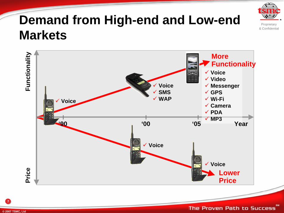
7
Func
tiona
lity
‘90 ‘‘00 ‘05
VoiceSMSWAPVoice
Pric
e
Voice
VoiceLowerPrice
Demand from High-end and Low-end Markets
VoiceVideoMessengerGPSWi-FiCameraPDAMP3
MoreFunctionality
Year

Proprietary& Confidential
© 2007 TSMC, Ltd
8
In Search of A PC to Serve “The Next Billion”
INTEL“ClassMate”
One Laptop Per Child“XO”
ASUS“Eee”
The low-cost PCs for the developing nations:

Proprietary& Confidential
© 2007 TSMC, Ltd
9
Growth Opportunities are Global
Source: “The fortune at the bottom of the pyramid” by C. K. Prahalad, and IMF
Developing(Base of the Pyramid)
Emerging
Population (millions)
800
1,500
4,000Basic functions
Feature-rich & connected
Product FocusPr
ice/ F
eatu
re/
Perfo
rman
ce
Spec
trum
Advanced

Proprietary& Confidential
© 2007 TSMC, Ltd
10
-5
5
15
25
35
45
55
65
Plenty of Opportunity Ahead
Source: US Census Bureau; IC-Insights; TSMC estimates
10
11
Wor
ld P
opul
atio
n (B
illio
n)
Sem
i $ /
Pers
on
5
6
7
8
9
‘80 ‘85 ‘90 ‘95 ‘00 ‘05 ‘10
US Semi / Person = ~$250245
255
265
China & India Semi / Person = ~$20
4
Worldwide average semiconductor $ per personWorld Population

Proprietary& Confidential
© 2007 TSMC, Ltd
11
Outline
Semiconductor Market OutlookChallenges and Solutions
EconomicTechnology
Summary

Proprietary& Confidential
© 2007 TSMC, Ltd
12
Challenges
Economic
1. Huge CapEx2. ROI Risk – Process3. ROI Risk – Product
Technology
4. Nanometer Manufacturing5. Nanometer Design6. Design Complexity
Proprietary& Confidential
© 2007 TSMC, Ltd
13
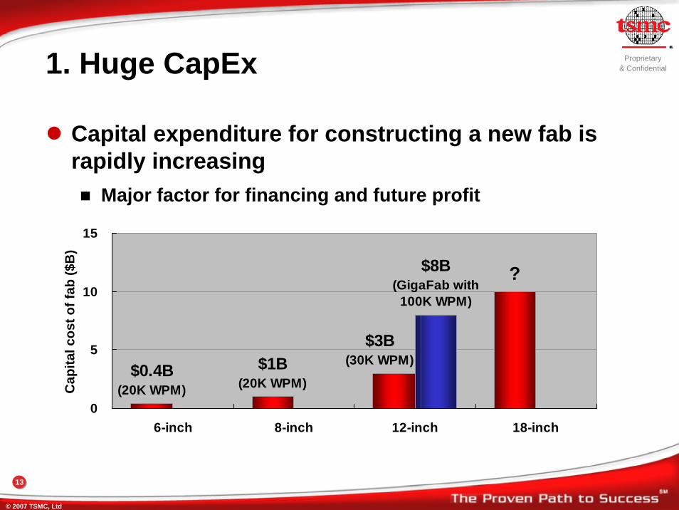
1. Huge CapEx
Capital expenditure for constructing a new fab is rapidly increasing
Major factor for financing and future profit
$0.4B(20K WPM)
$1B(20K WPM)
$3B(30K WPM)
?$8B(GigaFab with
100K WPM)
0
5
10
15
6-inch 8-inch 12-inch 18-inch
Cap
ital c
ost o
f fab
($B
)

Proprietary& Confidential
© 2007 TSMC, Ltd
14
PastPast
OEM
Distribution
Solution – Foundry Based Business Model
Many IDMs are changing to either fab-lite of fablessA wide variety of consolidation and collaboration are inevitable
FutureFuture
Assembly& Test
Design Service
IP Vendor Fabless
PresentPresent
Manufacturer
Product
Design Product Focused
IDM
IDM Getting Fab-lite Assembly
& Test
Foundry
IP Vendor
Fabless
Few IDMs
Few Foundries
Few IDMs & Foundries,Many Fabless
VerticallyIntegrated
IDMs in Transition,Fabless Getting Bigger
Proprietary& Confidential
© 2007 TSMC, Ltd
15
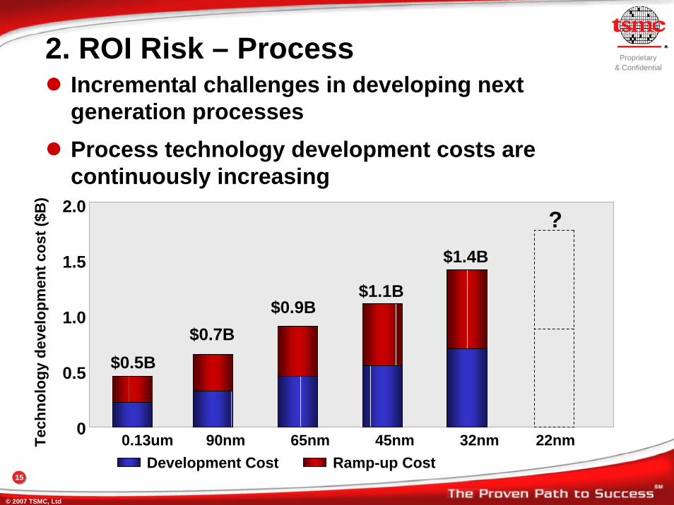
2. ROI Risk – ProcessIncremental challenges in developing next generation processesProcess technology development costs are continuously increasing
22nm0.13um 90nm
$0.5B$0.7B
65nm
$0.9B
45nm
$1.1B
32nm
$1.4B
Ramp-up CostDevelopment Cost
Tech
nolo
gy d
evel
opm
ent c
ost (
$B)
0.5
0
1.0
1.5
2.0 ?
Proprietary& Confidential
© 2007 TSMC, Ltd
16
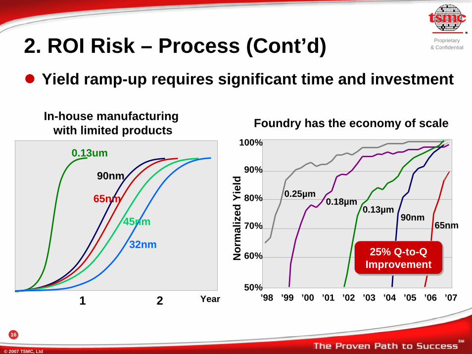
2. ROI Risk – Process (Cont’d)Yield ramp-up requires significant time and investment
50%
60%
70%
80%
90%
’98 ’99 ’00 ’01 ’02 ’03 ’04 ’05 ’06 ’07
Nor
mal
ized
Yie
ld
0.25µm0.18µm
0.13µm90nm
65nm
25% Q-to-QImprovement25% Q-to-Q
Improvement
100%
1 2 Year
0.13um
45nm
90nm
32nm
65nm
In-house manufacturing with limited products Foundry has the economy of scale

Proprietary& Confidential
© 2007 TSMC, Ltd
17
Solution I – Technology Alliance
Collaboration is required to overcame ever –increasing financial as well as technical challenges
IMEC
Matsushita

Proprietary& Confidential
© 2007 TSMC, Ltd
18
Solution II – Collaboration among Foundry, IP/EDA Vendors, And Design Service Suppliers
Standardization of IP & EDA tools
IDM
IP & EDADesign Service
Foundries

Proprietary& Confidential
© 2007 TSMC, Ltd
19
3. ROI Risks - ProductDesign complexity and cost increase rapidlyShort time to market
0.13um 90nm 65nm 45nm
10
20
30
40 80
60
40
209M$9.2M
16M
$18M
27M$48M
Gat
e C
ount
(M)
Des
ign
Cos
t ($M
)
Design CostGate Count
40M$70M
Proprietary& Confidential
© 2007 TSMC, Ltd
20
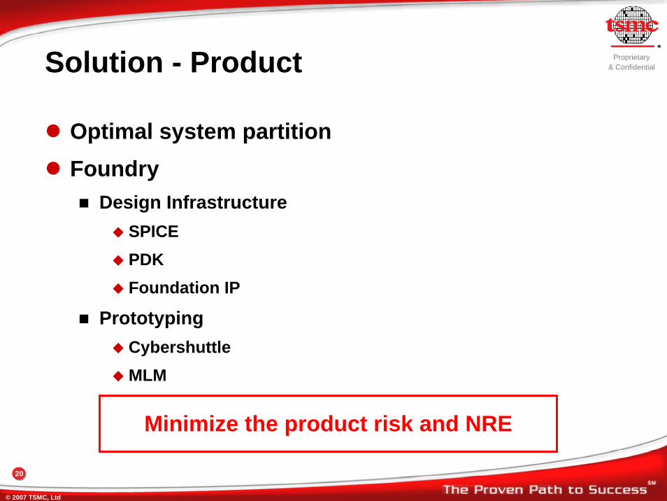
Solution - Product
Optimal system partitionFoundry
Design InfrastructureSPICEPDKFoundation IP
PrototypingCybershuttle MLM
Minimize the product risk and NRE

Proprietary& Confidential
© 2007 TSMC, Ltd
21
4. Nanometer Manufacturing
New materials and device structureHigh-K gate dielectric Metal gate3D FINFETLow-K Interconnect
New EDA solutions for technology modeling and advanced lithography

Proprietary& Confidential
© 2007 TSMC, Ltd
22
Solution – Technology Modeling / Advanced Lithography
Secure accurate SPICE modeling
Modeling in new material, 3D device and equipment / topographyPolarization, OPC, double exposure and mask 3D effects
Accuracy
Systematiceffect
Randomeffect
STIWPEStrained silicon effectOPC
Corner modelStatistical model
Collaborate with EDA vendors to achieve seamless interfacing hierarchy

Proprietary& Confidential
© 2007 TSMC, Ltd
23
5. Design for Nanometer
Increasing systematic / parameter / random yield loss due to process variation
Physical patterning effects, open and short, etc.Chemical and mechanical impact, planarity, antenna effect, and via opens, etc.Timing, signal integrity and voltage drop
Increasing leakage (quantity, source, variation)
Proprietary& Confidential
© 2007 TSMC, Ltd
24
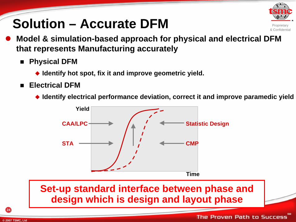
Solution – Accurate DFMModel & simulation-based approach for physical and electrical DFM that represents Manufacturing accurately
Physical DFMIdentify hot spot, fix it and improve geometric yield.
Electrical DFMIdentify electrical performance deviation, correct it and improve paramedic yield
Statistic Design
Time
CAA/LPC
STA CMP
Yield
Set-up standard interface between phase and design which is design and layout phase

Proprietary& Confidential
© 2007 TSMC, Ltd
25
Solution – DFM Ecosystem
Foundry to set up DFM ecosystem and open license DUF to reduce costStandard interface between the design infrastructure and manufacturing
EDA Alliance IP/Lib Alliance TSMC TSMC/GUC +DCA Alliance
TSMC DFM Compliance Initiative
Example:
Proprietary& Confidential
© 2007 TSMC, Ltd
26
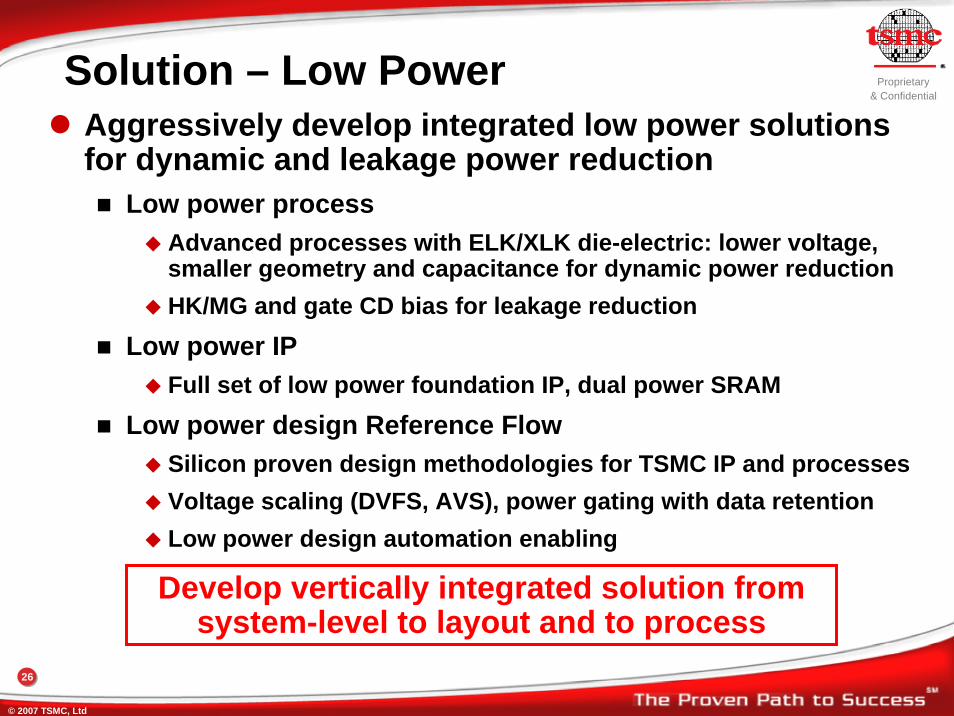
Solution – Low PowerAggressively develop integrated low power solutions for dynamic and leakage power reduction
Low power processAdvanced processes with ELK/XLK die-electric: lower voltage, smaller geometry and capacitance for dynamic power reductionHK/MG and gate CD bias for leakage reduction
Low power IPFull set of low power foundation IP, dual power SRAM
Low power design Reference Flow Silicon proven design methodologies for TSMC IP and processesVoltage scaling (DVFS, AVS), power gating with data retention Low power design automation enabling
Develop vertically integrated solution from system-level to layout and to process

Proprietary& Confidential
© 2007 TSMC, Ltd
27
6. Design ComplexityIncreased design complexity causes longer time-to-market and requires significant effort for verification and software design
‘95 ‘00 ‘05 ‘10 ‘15 ‘20
Moore’s Law
Mobile Multimedia DeviceCommunication Device
Current Design Productivity
VGA
D1
HD
Full HD
2G
3G
4G
Year
Com
plex
ity

Proprietary& Confidential
© 2007 TSMC, Ltd
28
ElectronicSystem Level (ESL)
Main Stream
ICE
AMBA Multi-layer AHBAMBA Multi-layer AHB
AMBA APBAMBA APB
APB BridgeAPB
Bridge
GPIOGPIOPWMPWM KBMOUSE
KBMOUSE WDTWDT I2CI2CDAI
(I2S)DAI (I2S) TimerTimer RTCRTC UARTUARTSSISSI
StaticMemory
Controller
StaticMemory
Controller
DirectMemoryAccess
DirectMemoryAccess
VectorInterrupt
Controller
VectorInterrupt
Controller
LocalMemory
Controller
LocalMemory
Controller
SDRAMController
(4-CH)
SDRAMController
(4-CH)
GPrimeGPrime PlatformPlatform
CPUCPU
Network
Architecture ExplorationSoftware ProfilingHardware ProfilingPower Estimation
Main Stream vs.ESL Co-development Environment
Proprietary& Confidential
© 2007 TSMC, Ltd
29
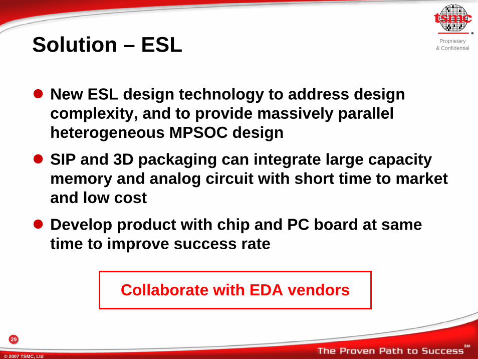
Solution – ESL
New ESL design technology to address design complexity, and to provide massively parallel heterogeneous MPSOC designSIP and 3D packaging can integrate large capacity memory and analog circuit with short time to market and low costDevelop product with chip and PC board at same time to improve success rate
Collaborate with EDA vendors

Proprietary& Confidential
© 2007 TSMC, Ltd
30
Summary
Semiconductor market growth will continue but moderate Future growth opportunities will be global but bifurcateHigh ROI risks in design, fab, and technology could be alleviated with the integrated foundry modelClose collaboration is required between EDA vendors, foundry and IC companies
Proprietary& Confidential
© 2007 TSMC, Ltd
www.tsmc.com
Thank You