the future of data storage technologies · the future of data storage technologies sadik c. esener...
TRANSCRIPT

International Technology Research Institute World Technology (WTEC) Division
WTEC Panel Report on
The Future of Data Storage Technologies
Sadik C. Esener (Panel Co-Chair)Mark H. Kryder (Panel Co-Chair)William D. DoyleMarvin KeshnerMasud MansuripurDavid A. Thompson
June 1999
International Technology Research InstituteR.D. Shelton, Director
Geoffrey M. Holdridge, WTEC Division Director and ITRI Series Editor
4501 North Charles StreetBaltimore, Maryland 21210-2699
WTEC Panel on the Future of Data Storage Technologies
Sponsored by the National Science Foundation, Defense Advanced Research Projects Agencyand National Institute of Standards and Technology of the United States government.
Dr. Sadik C. Esener (Co-Chair)Prof. of Electrical and Computer Engineering & Material SciencesDept. of Electrical & Computer EngineeringUniversity of California, San Diego9500 Gilman DriveLa Jolla, CA 92093-0407
Dr. Mark H. Kryder (Co-Chair)Director, Data Storage Systems CenterCarnegie Mellon UniversityRoberts Engineering Hall, Rm. 348Pittsburgh, PA 15213-3890
Dr. William D. DoyleDirector, MINT CenterUniversity of AlabamaBox 870209Tuscaloosa, AL 35487-0209
Dr. Marvin KeshnerDirector, Information Storage LaboratoryHewlett-Packard Laboratories1501 Page Mill RoadPalo Alto, CA 94304-1126
Dr. Masud MansuripurOptical Science CenterUniversity of ArizonaTucson, AZ 85721
Dr. David A. ThompsonIBM FellowResearch DivisionInternational Business Machines CorporationAlmaden Research CenterMail Stop K01/802650 Harry RoadSan Jose, CA 95120-6099
INTERNATIONAL TECHNOLOGY RESEARCH INSTITUTEWorld Technology (WTEC) Division
WTEC at Loyola College (previously known as the Japanese Technology Evaluation Center, JTEC) provides assessmentsof foreign research and development in selected technologies under a cooperative agreement with the National ScienceFoundation (NSF). Loyola’s International Technology Research Institute (ITRI), R.D. Shelton, Director, is the umbrellaorganization for WTEC. Elbert Marsh, Deputy Assistant Director for Engineering at NSF’s Engineering Directorate, isNSF Program Director for WTEC. Several other U.S. government agencies provide support for the program through NSF.
WTEC’s mission is to inform U.S. scientists, engineers, and policymakers of global trends in science and technology in amanner that is timely, credible, relevant, efficient, and useful. WTEC’s role is central to the government’s effort tomeasure its performance in science and technology. Panels of typically six technical experts conduct WTEC assessments.Panelists are leading authorities in their field, technically active, and knowledgeable about U.S. and foreign researchprograms. As part of the assessment process, panels visit and carry out extensive discussions with foreign scientists andengineers in their labs.
The ITRI staff at Loyola College helps select topics, recruits expert panelists, arranges study visits to foreign laboratories,organizes workshop presentations, and finally, edits and disseminates the final reports.
Dr. R.D. Shelton Mr. Geoff Holdridge Dr. George GamotaITRI Director WTEC Division Director ITRI Associate DirectorLoyola College Loyola College 17 Solomon Pierce RoadBaltimore, MD 21210 Baltimore, MD 21210 Lexington, MA 02173

WTEC Panel on
The Future of Data Storage Technologies
FINAL REPORT
June 1999
Sadik C. Esener (Panel Co-Chair)Mark H. Kryder (Panel Co-Chair)William D. DoyleMarvin KeshnerMasud MansuripurDavid A. Thompson
ISBN 1-883712-53-xThis document was sponsored by the National Science Foundation (NSF), Defense Advanced Research Projects Agency(DARPA) and National Institute of Standards and Technology (NIST) of the U.S. government under NSF CooperativeAgreement ENG-9707092, awarded to the International Technology Research Institute at Loyola College in Maryland. Thegovernment has certain rights to this material. Any opinions, findings, and conclusions or recommendations expressed in thismaterial are those of the authors and do not necessarily reflect the views of the United States government, the authors’ parentinstitutions, or Loyola College.

ABSTRACT
This report reviews the status of Japanese high-density data storage technology, manufacturing and R&D incomparison to that in the United States. It covers various optical data storage technologies, magnetic hard diskdrives, and magnetic tape drives, as well as the emerging long-term data storage technology alternatives.Information sources used in the study include literature review, site visits in Japan, and a review of the draft reportby panelists, site visit hosts, and study sponsors. It also includes information obtained from presentations from U.S.panelists and Japanese counterparts given at a workshop that took place in Tokyo prior to the site visits. Theorganizations chosen for site visits were those that have established a leadership role in some important aspect ofdata storage technology. In all, the panelists visited 15 Japanese institutions including 5 companies and onegovernment organization involved in optical data storage only, 4 companies focused on magnetic data storage only,and 5 companies that are heavily involved in both magnetic and optical data storage. The panel found that Japanclearly leads in optical data storage and magnetic tape drives, both countries are competitive in magnetic hard diskdrives, and researchers in both countries are clearly aware of future challenges in data storage technologies for thenext decade. Both the United States and Japan put significant emphasis on long-range alternative data storagetechniques. There are clear possibilities for Japan to surpass the United States in the hard disk drive segment andopportunities for the United States to catch up in optical data storage. Japanese government funding in data storagein general appears to far outstrip comparable government funding in the United States. In optical data storage, withJapan being in a comfortable leading position, most R&D funding is derived from industrial sources, although newlarge government programs in this area are being started. However, there is substantial present government andindustrial support for R&D in magnetic hard disk drives where Japan trails the United States.
International Technology Research Institute (ITRI)
R. D. Shelton, Principal Investigator, ITRI DirectorGeorge Mackiw, Deputy ITRI Director
George Gamota, ITRI Associate DirectorJ. Brad Mooney, TTEC Division Director
Robert Margenthaler, BD Division Director
World Technology (WTEC) Division
Geoffrey M. Holdridge, WTEC Division DirectorBobby A. Williams, Financial Officer
Aminah Grefer, Editorial AssistantCatrina M. Foley, Administrative Assistant
Christopher McClintick, Head of Publications SectionRoan E. Horning, Professional Assistant, Web Administrator
Michael Stone, LINUX Systems AdministratorSarah Mayne, Student Assistant
Gerald Whitman, Japan Advance ContractorHiroshi Morishita, WTEC Japan Representative
Copyright 1999 by Loyola College in Maryland except where otherwise noted. This work relates to NSF Cooperative AgreementENG-9707092. The U.S. government retains a nonexclusive and nontransferable license to exercise all exclusive rights provided bycopyright. The ISBN number for this report is 1-883712-53-x. This report is distributed by the National Technical InformationService (NTIS) of the U.S. Department of Commerce as NTIS report PB99-144214 . A list of available WTEC reports is included onthe inside back cover of this report. Recent reports are posted on the Internet at http://itri.loyola.edu.
i
FOREWORD
Timely information on scientific and engineering developments occurring in laboratories around the worldprovides a critical input to maintaining the economic and technological strength of the United States.Moreover, sharing this information quickly with other countries can greatly enhance the productivity ofscientists and engineers. These are some of the reasons why the National Science Foundation (NSF) hasbeen involved in funding science and technology assessments comparing the United States and foreigncountries since the early 1980s. A substantial number of these studies have been conducted by the WorldTechnology Evaluation Center (WTEC) Division, managed by Loyola College through a cooperativeagreement with the National Science Foundation.
The purpose of the WTEC activity is to assess research and development efforts in other countries in specificareas of technology, to compare these efforts and their results to U.S. research in the same areas, and toidentify opportunities for international collaboration in precompetitive research.
Many U.S. organizations support substantial data gathering and analysis efforts focusing on nations such asJapan. But often the results of these studies are not widely available. At the same time, government andprivately sponsored studies that are in the public domain tend to be “input” studies. They enumerate inputsto the research and development process, such as monetary expenditures, personnel data, and facilities, butdo not provide an assessment of the quality or quantity of the outputs obtained. Studies of the outputs of theresearch and development process are more difficult to perform because they require a subjective analysisperformed by individuals who are experts in the relevant scientific and technical fields. The NSF staffincludes professionals with expertise in a wide range of disciplines. These individuals provide the expertiseneeded to assemble panels of experts who can perform competent, unbiased reviews of research anddevelopment activities. Specific technologies such as telecommunications, biotechnology, andnanotechnology are selected for study by government agencies that have an interest in obtaining the resultsof an assessment and are able to contribute to its funding. A typical WTEC assessment is sponsored byseveral agencies.
In the first few years of this activity, most of the studies focused on Japan, reflecting interest in that nation'sgrowing economic prowess. The program was then called JTEC (Japanese Technology Evaluation Center).Beginning in 1990, we began to broaden the geographic focus of the studies. As interest in the EuropeanCommunity (now the European Union) grew, we added Europe as an area of study. With the breakup of theformer Soviet Union, we began organizing visits to previously restricted research sites opening up there.Most recently, studies have begun to focus also on emerging science and technology capabilities in Asiancountries such as the People's Republic of China.
In the past several years, we also have begun to substantially expand our efforts to disseminate information.Attendance at WTEC workshops (in which panels present preliminary findings) has increased, especiallyindustry participation. Representatives of U.S. industry now routinely number 50% or more of the totalattendance, with a broad cross-section of government and academic representatives making up theremainder. Publications by WTEC panel members based on our studies have increased, as have the numberof presentations by panelists at professional society meetings.
The WTEC program will continue to evolve in response to changing conditions. New global informationnetworks and electronic information management systems provide opportunities to improve both the contentand timeliness of WTEC reports. We are now disseminating the results of WTEC studies via the Internet.Twenty-six of the most recent WTEC final reports are now available on the World Wide Web(http://itri.loyola.edu) or via anonymous FTP (ftp.wtec.loyola.edu/pub/). Viewgraphs from several recentworkshops are also on the Web server.
Forewordii
As we seek to refine the WTEC activity, improving the methodology and enhancing the impact, programorganizers and participants will continue to operate from the same basic premise that has been behind theprogram from its inception, i.e., that improved awareness of international developments can significantlyenhance the scope and effectiveness of international collaboration and thus benefit the United States and allits international partners in collaborative research and development efforts.
Paul J. HererNational Science Foundation

iii
TABLE OF CONTENTS
Foreword............................................................................................................................................................. iTable of Contents.............................................................................................................................................. iiiList of Figures.................................................................................................................................................... vList of Tables .................................................................................................................................................... vi
Executive Summary....................................................................................................................................... vii
1. Introduction Optical StorageSadik C. Esener
Optical Recording Technology and Applications ............................................................................... 1Optical Storage Market........................................................................................................................ 5Summary of Technology Status .......................................................................................................... 7Long-Term Outlook ............................................................................................................................ 8
2. Introduction Magnetic Recording TechnologyMark H. Kryder
Introduction ....................................................................................................................................... 11Magnetic Disk Drive Applications and Markets ............................................................................... 12Magnetic Disk Drive Technology Status ..........................................................................................13Magnetic Tape Drive Applications and Markets............................................................................... 15Magnetic Tape Drive Technology Status ..........................................................................................17
3. Magnetic Disk TechnologiesDavid A. Thompson
Introduction ....................................................................................................................................... 19Long Term Strategies ........................................................................................................................ 22Conclusions ....................................................................................................................................... 26References ......................................................................................................................................... 27
4. Magnetic Tape StorageWilliam D. Doyle
Background ....................................................................................................................................... 29Future Tape Technology ................................................................................................................... 30Head Technology .............................................................................................................................. 31Electronics ......................................................................................................................................... 31New Media ........................................................................................................................................ 32Head-Media Interface........................................................................................................................ 33Critical Issues .................................................................................................................................... 34
5. R&D Activities in Optical Data Storage MediaMasud Mansuripur
Background ....................................................................................................................................... 35An Overview of the Field of Optical Disk Data Storage................................................................... 35Reports of Visits to Industrial Laboratories in Japan ........................................................................ 52Summary ........................................................................................................................................... 56References ......................................................................................................................................... 56
Table of Contentsiv
6. Status of Optical Storage in JapanMarvin Keshner
Introduction....................................................................................................................................... 59Standards and Compatibility ............................................................................................................. 59Roadmaps for Optical Storage .......................................................................................................... 60Phase Change Optical Recording...................................................................................................... 60Magneto Optic Recording ................................................................................................................. 61Which Technology Will Win? .......................................................................................................... 62Is 45 GB Per Side Good Enough?..................................................................................................... 62Beyond Video Disks and Beyond 100 GB Per Disk......................................................................... 62
7. Alternative Storage TechnologiesSadik Esener and Mark Kryder
Introduction....................................................................................................................................... 65Long Range Applications Pull .......................................................................................................... 66Long Term Technology Push............................................................................................................ 67Technology Comparison ................................................................................................................... 81Conclusion ........................................................................................................................................ 83References......................................................................................................................................... 84
APPENDICES
A. Professional Experience of Panel Members.................................................................................. 85
B. Professional Experience of Other Team Members...................................................................... 88
C. Site Reports...................................................................................................................................... 90
Canon Research Center ..................................................................................................................... 90Fujitsu Laboratories, Ltd. (HDD presentations)................................................................................ 93Fujitsu Laboratories, Ltd. (optical storage presentations)................................................................. 96Fuji Electric Co., Ltd....................................................................................................................... 101Fujifilm............................................................................................................................................ 103Hitachi Central Research Laboratory (optical storage presentations) ............................................ 106Hitachi Central Research Laboratory (magnetic storage presentations) ......................................... 110Matsushita Electric Industrial Co., Ltd. .......................................................................................... 113National Institute for Advanced Interdisciplinary Research ........................................................... 115Nikon Corporation .......................................................................................................................... 117Olympus Technology Research Institute ........................................................................................ 119Pioneer Corporation ........................................................................................................................ 120Sanyo Corporation .......................................................................................................................... 122Sony Corporation R&D Center (magnetic storage presentations). ................................................. 124Sony Corporation R&D Center (optical storage presentations)...................................................... 127TDK Corporation ............................................................................................................................ 129Toshiba Corporation (optical storage presentations) ...................................................................... 131Toshiba Corporation (magnetic storage presentations)................................................................... 133Yamaha Corporation ....................................................................................................................... 135
D. Glossary.......................................................................................................................................... 137
v
LIST OF FIGURES
ES.1 Worldwide disk drive sales revenue.................................................................................................xiii
1.1 Key components of an optical disk system ......................................................................................... 11.2 Potential evolution of application requirements for removable storage.............................................. 31.3 Capacity and data rate requirements.................................................................................................... 41.4a Comparison of worldwide hard disk and optical disk storage revenues ............................................. 61.4b Disparity in number of U.S. and Asian optical drive manufacturers .................................................. 61.5 Distribution of number of CD-ROM and optical library manufacturers............................................. 61.6 Respective removable media market share distribution in Japan in 1997........................................... 71.7 Examples of roadmaps ........................................................................................................................ 81.8 Potential roadmap for mastering technology....................................................................................... 81.9 Alternative optical storage technologies.............................................................................................. 9
2.1 Schematic diagram of a magnetic recording system ......................................................................... 122.2 Market share of non-U.S. and U.S. manufacturers of disk drives..................................................... 132.3 Areal density of magnetic hard disk drives ....................................................................................... 142.4 Schematic diagram of a perpendicular magnetic recording medium ................................................ 152.5 User application segments for magnetic tape.................................................................................... 162.6 Cost in $/GB of storage .................................................................................................................... 18
3.1 U.S. And non-U.S. HDD market share per year .............................................................................. 203.2 Areal density roadmap....................................................................................................................... 233.3 ASET/SRC areal density projection.................................................................................................. 233.4 Possible microactuator designs.......................................................................................................... 243.5 TDK microactuator............................................................................................................................ 243.6 Storage materials ............................................................................................................................... 253.7 ASET/SCR storage issues ................................................................................................................. 253.8 Storage media materials and efficiencies .......................................................................................... 263.9 Perpendicular magnetic recording with a single-pole head............................................................... 26
4.1 Storage subsystem cost trend ............................................................................................................ 304.2 High performance tape media ........................................................................................................... 324.3 Substrate stability-capacity/date rate trade-offs................................................................................. 34
5.1 Basic configuration of an optical disk system................................................................................... 375.2 Single-element aspherics lenses used in optical disk drives.............................................................. 395.3 Astigmatic focus-error detection system........................................................................................... 405.4 Recordable optical disks.................................................................................................................... 425.5 Track-error signal generated by push-pull method ........................................................................... 425.6 Small section of a simplified magneto-optical disk........................................................................... 445.7 Solid immersion lens ......................................................................................................................... 475.8a Typical pattern of land-groove recording.......................................................................................... 495.8b Cross-talk signal from a model ......................................................................................................... 495.9a Exchange-coupled magnetic trilayer ................................................................................................. 505.9b Cross-section view of magnetic domains .......................................................................................... 505.10 Exchange-coupled magnetic multi-layer used in magnetic super resolution .................................... 51
6.1 Road map for phase change disks ..................................................................................................... 616.2 Areal density vs. technology ............................................................................................................ 63
List of Figures, List of Tablesvi
7.1 Potential evolution of application requirements for removable storage............................................ 667.2 Estimates for possible areal densities ............................................................................................... 677.3 New degrees of freedom in data storage ........................................................................................... 687.4 Probe storage: a combination of sensing and modulation techniques.............................................. 707.5 Recording by STM/AFM probe in organic LB films........................................................................ 727.6 Probe storage at Canon ..................................................................................................................... 727.7 Probe storage at Matsushita .............................................................................................................. 737.8 Low-cost manufacture of probe tips ................................................................................................. 737.9 Thermo-mechanical recording at IBM.............................................................................................. 747.10 Classification and demonstrated performance of probe ................................................................... 747.11 Multi-layer optical disk stack............................................................................................................ 757.12 Double layer MO disk recording and readout................................................................................... 767.13 Principle of two-photon recording in 3D .......................................................................................... 777.14 Multi-layer 3D ROM disks reader/side view of a disk ..................................................................... 777.15 Potential impact of 3D multi-layer optical storage ........................................................................... 787.16 Multi-beam optical head investigated at Fujitsu ............................................................................... 807.17 Use of a VCSEL for recording and readout in a near field optics geometry .................................... 807.18 Schematic of a VCSEL array access ................................................................................................. 817.19 Roadmap for mastering and replication ............................................................................................ 817.20 Possible road map for alternative technologies.................................................................................827.21 Potential evolution of capacity vs. transfer rate ............................................................................... 83
LIST OF TABLES
ES.1 Optical Data Storage Technologies: State of the Art in Japan and the United States. ....................... xES.2 Magnetic Disk DrivesComparison of the United States and Japan................................................ xi
2.1 1996 Revenues from Tape Drive Sales............................................................................................. 17
3.1 Share of HDD Market by National Origin (1995) ............................................................................ 213.2 Location of HDD Final Assembly (1995)......................................................................................... 213.3 Geographical Distribution of the Wage Bill ..................................................................................... 213.4 Recent HeadlinesTypical Press Clippings..................................................................................... 213.5 Introduction of MR Heads by Company........................................................................................... 223.6 Current Areal Density by Company.................................................................................................. 22
4.1 Tape Density Projections .................................................................................................................. 304.2 Requirements for 4.7 Terabyte/in3 .................................................................................................... 314.3 Thinner Substrates............................................................................................................................. 33
7.1 Emerging Technologies and Applications ........................................................................................ 83

vii
EXECUTIVE SUMMARY
This report reviews the status of Japanese high-density data storage technology, manufacturing and R&D incomparison to that in the United States. It covers various optical data storage technologies, magnetic harddisk drives, and magnetic tape drives. Information sources used in the study include literature review, visitsto 15 relevant sites in Japan, a review of the draft reports by panelists, site visit hosts, and study sponsors.The report also includes information obtained from presentations from U.S. panelists and Japanesecounterparts given at a workshop that took place in Tokyo prior to the site visits.
The panel found that Japan clearly leads in optical data storage and magnetic tape drives, the United Statesand Japan are competitive in magnetic hard disk drives, and researchers in both countries are clearly aware offuture challenges in data storage technologies for the next decade. Both the United States and Japan putsignificant emphasis on long-range alternative data storage techniques.
There are clear possibilities for Japan to surpass the United States in the hard disk drive segment andopportunities for the United States to catch up in optical data storage. Japanese government funding in datastorage in general appears to far outstrip comparable government funding in the United States. In opticaldata storage, with Japan being in a comfortable leading position, most R&D funding is derived fromindustrial sources, although new large government programs in this area are being started. However, there issubstantial present government and industrial support for R&D in magnetic hard disk drives where Japantrails the United States.
MISSION AND PROCEDURE
The purpose of this WTEC panel study of high-density data storage in Japan was to investigate and report onthe current status of Japanese data storage technologies compared to that in the United States. In particular,the panel’s mission was to assess status and directions of Japanese R&D in high-density data storagetechnologies, and to contrast them with approaches taken by the United States.
To meet this goal, the panel researched the professional literature of both countries, visited numerouscompanies and government organizations in Japan, attended workshops on emerging technologies in theUnited States, and organized a workshop in Japan with participants including academic researchers. Thisreport is a synthesis of the panel’s findings reached by identifying general directions that transcendinstitutional boundaries.
The WTEC panel focused its investigations on four main areas:
1. optical data storage technology
2. magnetic hard disk technology
3. magnetic tape technology
4. emerging long-term data storage technology alternatives
The organizations chosen for site visits have established a leadership role in some important aspect of datastorage technology. In all, the panelists visited 15 Japanese institutions including five companies and onegovernment organization involved in optical data storage only, four companies focused on magnetic datastorage only, and five companies that are heavily involved in both magnetic and optical data storage.
Executive Summaryviii
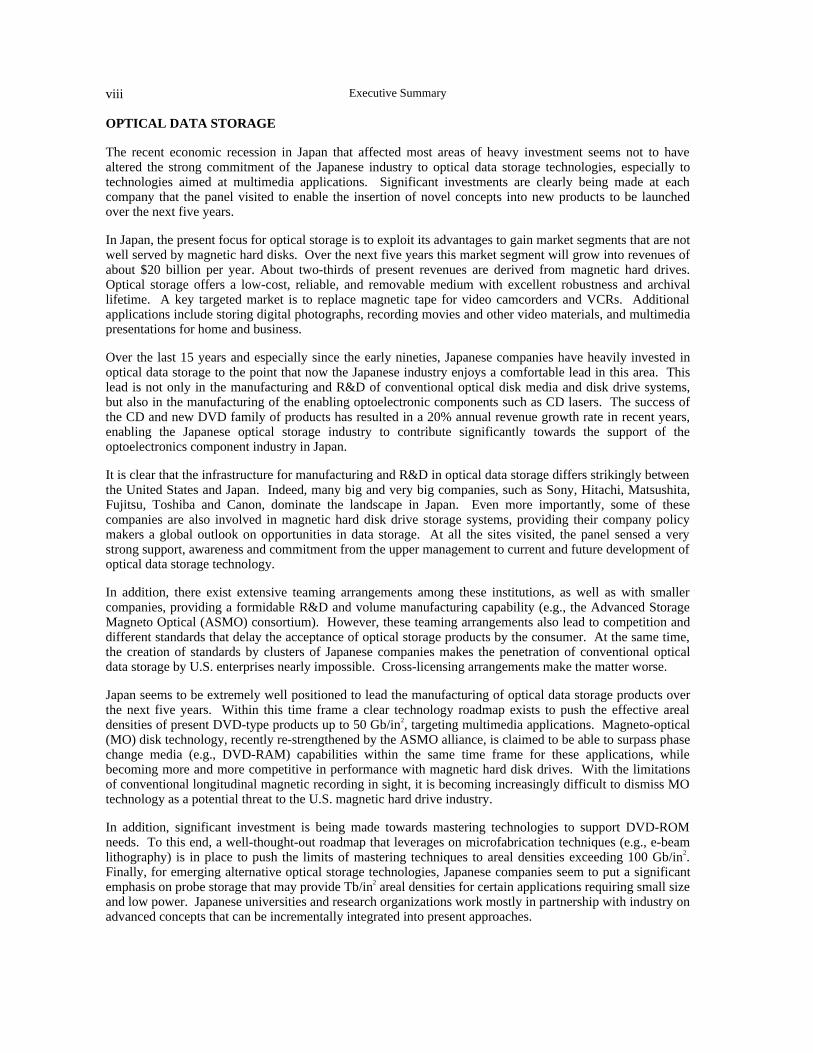
OPTICAL DATA STORAGE
The recent economic recession in Japan that affected most areas of heavy investment seems not to havealtered the strong commitment of the Japanese industry to optical data storage technologies, especially totechnologies aimed at multimedia applications. Significant investments are clearly being made at eachcompany that the panel visited to enable the insertion of novel concepts into new products to be launchedover the next five years.
In Japan, the present focus for optical storage is to exploit its advantages to gain market segments that are notwell served by magnetic hard disks. Over the next five years this market segment will grow into revenues ofabout $20 billion per year. About two-thirds of present revenues are derived from magnetic hard drives.Optical storage offers a low-cost, reliable, and removable medium with excellent robustness and archivallifetime. A key targeted market is to replace magnetic tape for video camcorders and VCRs. Additionalapplications include storing digital photographs, recording movies and other video materials, and multimediapresentations for home and business.
Over the last 15 years and especially since the early nineties, Japanese companies have heavily invested inoptical data storage to the point that now the Japanese industry enjoys a comfortable lead in this area. Thislead is not only in the manufacturing and R&D of conventional optical disk media and disk drive systems,but also in the manufacturing of the enabling optoelectronic components such as CD lasers. The success ofthe CD and new DVD family of products has resulted in a 20% annual revenue growth rate in recent years,enabling the Japanese optical storage industry to contribute significantly towards the support of theoptoelectronics component industry in Japan.
It is clear that the infrastructure for manufacturing and R&D in optical data storage differs strikingly betweenthe United States and Japan. Indeed, many big and very big companies, such as Sony, Hitachi, Matsushita,Fujitsu, Toshiba and Canon, dominate the landscape in Japan. Even more importantly, some of thesecompanies are also involved in magnetic hard disk drive storage systems, providing their company policymakers a global outlook on opportunities in data storage. At all the sites visited, the panel sensed a verystrong support, awareness and commitment from the upper management to current and future development ofoptical data storage technology.
In addition, there exist extensive teaming arrangements among these institutions, as well as with smallercompanies, providing a formidable R&D and volume manufacturing capability (e.g., the Advanced StorageMagneto Optical (ASMO) consortium). However, these teaming arrangements also lead to competition anddifferent standards that delay the acceptance of optical storage products by the consumer. At the same time,the creation of standards by clusters of Japanese companies makes the penetration of conventional opticaldata storage by U.S. enterprises nearly impossible. Cross-licensing arrangements make the matter worse.
Japan seems to be extremely well positioned to lead the manufacturing of optical data storage products overthe next five years. Within this time frame a clear technology roadmap exists to push the effective arealdensities of present DVD-type products up to 50 Gb/in2, targeting multimedia applications. Magneto-optical(MO) disk technology, recently re-strengthened by the ASMO alliance, is claimed to be able to surpass phasechange media (e.g., DVD-RAM) capabilities within the same time frame for these applications, whilebecoming more and more competitive in performance with magnetic hard disk drives. With the limitationsof conventional longitudinal magnetic recording in sight, it is becoming increasingly difficult to dismiss MOtechnology as a potential threat to the U.S. magnetic hard drive industry.
In addition, significant investment is being made towards mastering technologies to support DVD-ROMneeds. To this end, a well-thought-out roadmap that leverages on microfabrication techniques (e.g., e-beamlithography) is in place to push the limits of mastering techniques to areal densities exceeding 100 Gb/in2.Finally, for emerging alternative optical storage technologies, Japanese companies seem to put a significantemphasis on probe storage that may provide Tb/in2 areal densities for certain applications requiring small sizeand low power. Japanese universities and research organizations work mostly in partnership with industry onadvanced concepts that can be incrementally integrated into present approaches.
WTEC Panel on the Future of Data Storage Technologies ix
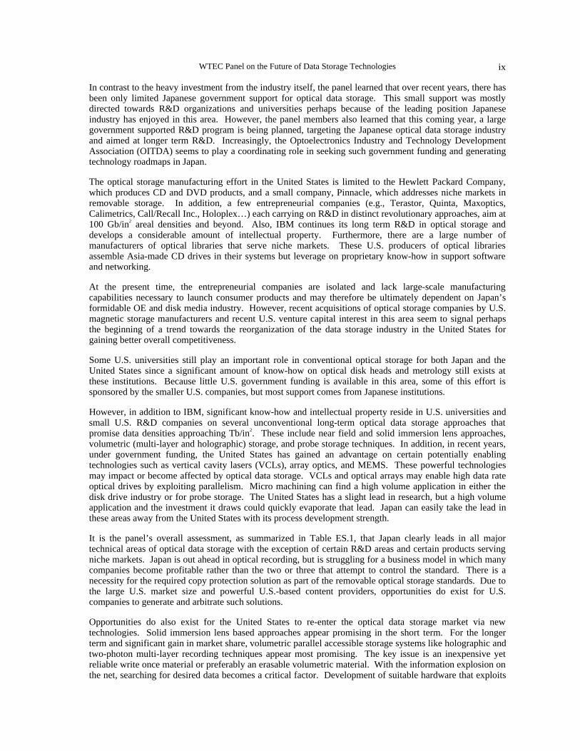
In contrast to the heavy investment from the industry itself, the panel learned that over recent years, there hasbeen only limited Japanese government support for optical data storage. This small support was mostlydirected towards R&D organizations and universities perhaps because of the leading position Japaneseindustry has enjoyed in this area. However, the panel members also learned that this coming year, a largegovernment supported R&D program is being planned, targeting the Japanese optical data storage industryand aimed at longer term R&D. Increasingly, the Optoelectronics Industry and Technology DevelopmentAssociation (OITDA) seems to play a coordinating role in seeking such government funding and generatingtechnology roadmaps in Japan.
The optical storage manufacturing effort in the United States is limited to the Hewlett Packard Company,which produces CD and DVD products, and a small company, Pinnacle, which addresses niche markets inremovable storage. In addition, a few entrepreneurial companies (e.g., Terastor, Quinta, Maxoptics,Calimetrics, Call/Recall Inc., Holoplex…) each carrying on R&D in distinct revolutionary approaches, aim at100 Gb/in2 areal densities and beyond. Also, IBM continues its long term R&D in optical storage anddevelops a considerable amount of intellectual property. Furthermore, there are a large number ofmanufacturers of optical libraries that serve niche markets. These U.S. producers of optical librariesassemble Asia-made CD drives in their systems but leverage on proprietary know-how in support softwareand networking.
At the present time, the entrepreneurial companies are isolated and lack large-scale manufacturingcapabilities necessary to launch consumer products and may therefore be ultimately dependent on Japan’sformidable OE and disk media industry. However, recent acquisitions of optical storage companies by U.S.magnetic storage manufacturers and recent U.S. venture capital interest in this area seem to signal perhapsthe beginning of a trend towards the reorganization of the data storage industry in the United States forgaining better overall competitiveness.
Some U.S. universities still play an important role in conventional optical storage for both Japan and theUnited States since a significant amount of know-how on optical disk heads and metrology still exists atthese institutions. Because little U.S. government funding is available in this area, some of this effort issponsored by the smaller U.S. companies, but most support comes from Japanese institutions.
However, in addition to IBM, significant know-how and intellectual property reside in U.S. universities andsmall U.S. R&D companies on several unconventional long-term optical data storage approaches thatpromise data densities approaching Tb/in2. These include near field and solid immersion lens approaches,volumetric (multi-layer and holographic) storage, and probe storage techniques. In addition, in recent years,under government funding, the United States has gained an advantage on certain potentially enablingtechnologies such as vertical cavity lasers (VCLs), array optics, and MEMS. These powerful technologiesmay impact or become affected by optical data storage. VCLs and optical arrays may enable high data rateoptical drives by exploiting parallelism. Micro machining can find a high volume application in either thedisk drive industry or for probe storage. The United States has a slight lead in research, but a high volumeapplication and the investment it draws could quickly evaporate that lead. Japan can easily take the lead inthese areas away from the United States with its process development strength.
It is the panel’s overall assessment, as summarized in Table ES.1, that Japan clearly leads in all majortechnical areas of optical data storage with the exception of certain R&D areas and certain products servingniche markets. Japan is out ahead in optical recording, but is struggling for a business model in which manycompanies become profitable rather than the two or three that attempt to control the standard. There is anecessity for the required copy protection solution as part of the removable optical storage standards. Due tothe large U.S. market size and powerful U.S.-based content providers, opportunities do exist for U.S.companies to generate and arbitrate such solutions.
Opportunities do also exist for the United States to re-enter the optical data storage market via newtechnologies. Solid immersion lens based approaches appear promising in the short term. For the longerterm and significant gain in market share, volumetric parallel accessible storage systems like holographic andtwo-photon multi-layer recording techniques appear most promising. The key issue is an inexpensive yetreliable write once material or preferably an erasable volumetric material. With the information explosion onthe net, searching for desired data becomes a critical factor. Development of suitable hardware that exploits

Executive Summaryx
parallel readout to facilitate content-based data search may point to a potential opportunity. In addition,investing in micro-mechanics for micro-actuators as well as for probe storage and creating a newinfrastructure in the United States to support future data storage approaches certainly appears compelling atthis time.
Table ES.1Optical Data Storage Technologies:
Comparison of State of the Art in Japan and the United States
Technology Japan
Status Trend
Conventional optical disks - Heads + ⇑
- Mastering + ⇑
- Media + ⇑
- Channels + ⇑
- Servos + ⇑
- Drive integration + ⇑
- Library integration − ⇒
ROM media = ⇑
Emerging non-conventional near-field optical disk technologies – Heads − ⇑
- Mastering + ⇑
- Media + ⇑
- Channels − ⇓
- Servos − ⇓
- Systems integration − ⇓
- Head-disk interface − ⇓
Probe storage - writing and reading = ⇒
- Media = ⇒
- Processing + ⇒
Holographic R&D − ⇓
2-Photon multi-layer disk R&D − ⇓
Supporting technologies – MEMS − ⇑
- Passive micro-optic assemblies + ⇑
- Advanced micro-optics − ⇓
- Mastering lasers = ⇒
- Optical media testers = ⇓
Key
+ Ahead of United States ⇑ Gaining ground
= Two countries even ⇓ Losing ground
− Behind United States ⇒ No change in trend
WTEC Panel on the Future of Data Storage Technologies xi
However, we should point out that except for low cost, personal, removable storage, which will be a sizablemarket over the next five years ($20 billion/year in revenues), optical storage will not be the dominanttechnology for storage. Magnetic disk drives will be. The United States should not lose this technology andits future investment base.
MAGNETIC STORAGE
In spite of the recent economic difficulties in Japan, it was found that Japanese companies are gainingstrength both technologically and marketwise in the area of magnetic data storage. For the past three yearsU.S. company market shares have decreased as a percentage of total, while Japanese company market shareshave increased. Furthermore, although U.S. companies still account for over 75% of magnetic hard diskdrive sales, a much larger percentage of the components used in those drives are made in Japan.
It was found that the Japanese government, companies and universities were making major commitments toresearch on advanced magnetic and other data storage. Twenty-one Japanese companies in the magnetic datastorage area are funding the Storage Research Consortium (SRC), which currently supports 34 Japaneseuniversities working toward demonstrating 20 Gb/in2 on a magnetic hard disk. Major funding of universityresearch in this area by Japanese companies is a relatively new phenomenon and was originally announced asa direct response to the success of the United States in creating centers for research on magnetic data storageat universities such as Carnegie Mellon University, the University of California at San Diego and StanfordUniversity. In addition, the Japanese government is providing ¥5 billion in funding to six industrial firms todevelop 40 Gb/in2 magnetic recording technology by funding the Association of Super-Advanced ElectronicsTechnologies (ASET) program through MITI. The SRC and ASET programs are coupled through theleadership of the six industrial firms and researchers, which are part of both programs.
Japanese companies were clearly aware of the long-term research issues such as barriers to increased storagedensity caused by thermal instabilities and had relatively large research programs addressing them. Bycomparison, with the exception of IBM, most U.S. companies are working only upon the next generation ortwo (1–3 years) of product and are relying upon their involvement in the National Storage IndustryConsortium or U.S. universities to deal with longer term (5–10 year) issues.
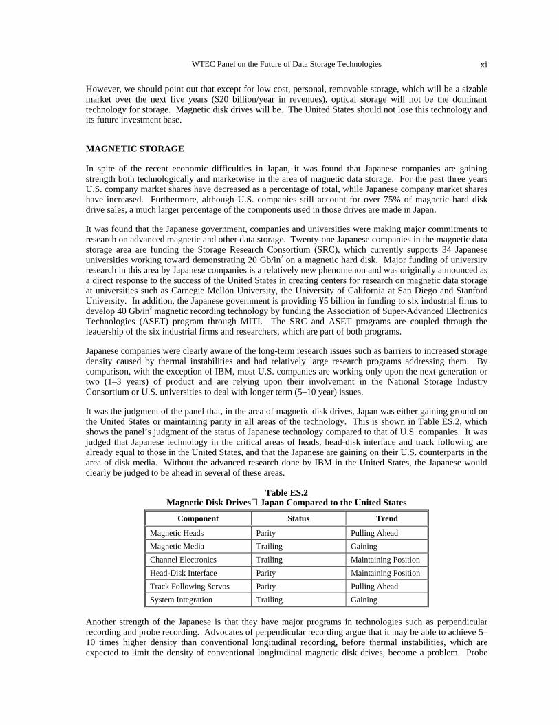
It was the judgment of the panel that, in the area of magnetic disk drives, Japan was either gaining ground onthe United States or maintaining parity in all areas of the technology. This is shown in Table ES.2, whichshows the panel’s judgment of the status of Japanese technology compared to that of U.S. companies. It wasjudged that Japanese technology in the critical areas of heads, head-disk interface and track following arealready equal to those in the United States, and that the Japanese are gaining on their U.S. counterparts in thearea of disk media. Without the advanced research done by IBM in the United States, the Japanese wouldclearly be judged to be ahead in several of these areas.
Table ES.2Magnetic Disk DrivesJapan Compared to the United States
Component Status Trend
Magnetic Heads Parity Pulling Ahead
Magnetic Media Trailing Gaining
Channel Electronics Trailing Maintaining Position
Head-Disk Interface Parity Maintaining Position
Track Following Servos Parity Pulling Ahead
System Integration Trailing Gaining
Another strength of the Japanese is that they have major programs in technologies such as perpendicularrecording and probe recording. Advocates of perpendicular recording argue that it may be able to achieve 5–10 times higher density than conventional longitudinal recording, before thermal instabilities, which areexpected to limit the density of conventional longitudinal magnetic disk drives, become a problem. Probe

Executive Summaryxii
recording on various media types has been shown to have potential of storing information at densities severalorders of magnitude higher than possible with longitudinal magnetic recording. Canon showed the WTECteam probe recording of 10 nm sized spots on Langmuir-Blodgett type media. Most U.S. disk drivecompanies have no activities in either perpendicular or probe recording.
In the area of magnetic tape drives, the Japanese have a critical advantage in that they are the only source ofhigh-performance recording tape. This leaves U.S. magnetic tape drive manufacturers critically dependentupon Japanese companies for tape media and is a serious threat to the development of future high-performance tape drive products. To develop advanced tape drives, it is necessary that all the components bedeveloped together and integrated. Currently, as Table ES.2 shows, U.S. companies are considered to havethe lead in magnetic heads, servos, signal processing and systems integration of tape drives for data storage,but if U.S. tape drive manufacturers are unable to obtain advanced tape media samples in the future, this leadcould disappear very quickly, because U.S. drive development will have to wait until suitable tape becomescommercially available, which could be long after competitors have developed their products. This situationis particularly perplexing, since advanced media development, including media substrates and head-mediainterface, are seen as the primary roadblocks to future progress in the technology. This problem is not easilysolved as there is currently only one viable tape media supplier in the United States, and it is not licensed forthe double-coat technology, which was developed by Fuji in Japan and which is currently the favoredapproach to making high-performance tape media.
FUTURE MARKETS
Advances in data storage technology are critical to computer technology; however, advances in data storagetechnology have been so rapid over the past several decades that it has been taken for granted by thecomputer industry. Areal density on magnetic hard disk drives has advanced over 2 million times since thefirst disk drive, the RAMAC, was introduced by IBM in 1957, and this has dramatically reduced cost of datastorage. In the last ten years alone, the average price per megabyte of information stored on disk has droppedfrom $12 to less than $0.1 as shown in Fig. ES.1, which plots past and projected future cost per megabyte ofdisk storage and total worldwide disk drive sales revenue from 1988 to 2000. This has fueled good growth inthe data storage industry, but, with the advent of computer networks, the demand for data storage isincreasing and the industry is projected to grow at an even more rapid pace in the future. The fact that anincreasing portion of the components of disk drives are being made in Japan, the recently institutedcooperative university-industry-government cooperative research programs in Japan, and the strength of theJapanese companies in long-term research on magnetic data storage compared to those in the United Statessuggest that Japanese companies will assume a larger portion of this future market. Indeed, Japan has gaineda larger percentage of the market for disk drives each of the last three years. The United States needs tomake a larger commitment to long-term research in this area and should consider working cooperatively withJapan in areas where both sides bring something to the program.

WTEC Panel on the Future of Data Storage Technologies xiii
Fig. ES.1. Trends in disk drive sales and cost per megabyte.
2005200019951990198520000
30000
40000
50000
60000
70000
80000
.01
.1
1
10
100
Sales RevenuePrice/MB
Year
Wor
ldw
ide
Dis
k D
rive
Sal
es R
even
ue (
$ m
illio
n)
Ave
rage
Pric
e pe
r M
egab
yte
($)

Executive Summaryxiv

1
CHAPTER 1
INTRODUCTIONOPTICAL STORAGE
Sadik C. Esener
OPTICAL RECORDING TECHNOLOGY AND APPLICATIONS
Optical storage systems consist of a drive unit and a storage medium in a rotating disk form. In general thedisks are pre-formatted using grooves and lands (tracks) to enable the positioning of an optical pick-up andrecording head to access the information on the disk. Under the influence of a focused laser beam emanatingfrom the optical head, information is recorded on the media as a change in the material characteristics, oftenusing a thermally induced effect. To record a bit, a small spot is generated on the media modulating thephase, intensity, polarization, or reflectivity of a readout optical beam which is subsequently detected by adetector in the optical head. The disk media and the pick-up head are rotated and positioned through drivemotors and servo systems controlling the position of the head with respect to data tracks on the disk.Additional peripheral electronics are used for control and data acquisition and encoding/decoding. Such asystem is illustrated in Fig. 1.1.
DISK MEDIA
MOVINGMICROLENS
TRACKINGFOCUSING
OPTO-ELECTRONICS
TRACKING / FOCUSINGSERVO
STORAGEMEDIA
Laser beamHead movement
Linear motor
Drive motor
CHANNEL ELECTRONICSAND ECC
PICK-UP HEAD
Fig. 1.1. Key components of an optical disk system.
1. IntroductionOptical Storage2
As for all storage systems, the storage capacity, data transfer rate, access time, and cost characterize opticaldisks systems. The storage capacity is a direct function of the spot size (the minimum dimensions of a storedbit) and the geometrical dimensions of the media. A good metric that measures the efficiency in using thestorage area is the areal density (Gb/in2). The areal density is governed by the resolution of the media and bythe numerical aperture of the optics and the wavelength of the laser in the optical head used for recording andread-out. The areal density can be limited by how well one can position the head over the tracks. The trackdensity (tracks/in) is used as a metric for this characteristic. In addition the areal density can be limited byhow close the optical transitions can be spaced. This is measured by the linear bit density (bits/in).
The data transfer rate is critical in applications where long data streams must be stored or retrieved such asin image storage or back-up applications. The linear density, the rotational speed of the drive, and thenumber of pickup heads determine data rate. It is often limited by the optical power available, the speed ofthe pick-up head servo controllers, and the tolerance of the media to high centrifugal forces.
The access time is a critical parameter in computing applications such as transaction processing andrepresents how fast a data location can be accessed on the disk. It is mostly governed by the latency of thehead movements and is proportional to the weight of the pick-up head and the rotation speed of the disk.
Finally, the cost of a drive, consisting of the drive cost and the media cost, strongly depends on the number ofunits produced, the automation techniques used during assembly, and component and overall system yields.
Optical storage offers a reliable and removable storage medium with excellent robustness and archivallifetime and with very low cost. A key difference between optical recording and magnetic recording is theease with which the optical media can be made removable. Both optical recording and readout can beperformed with a head positioned relatively far away from the storage medium, unlike magnetic hard driveheads. This allows the medium to be removable and effectively eliminates head crashes, increasingreliability. In addition, during recording, optical radiation is used as a focused thermal source allowing theuse of more stable materials suitable for archival lifetimes. On the other hand, the remote optical head isheavier and leads to slower access times when compared to hard disk drives.
Consequently optical storage has remained limited to market segments requiring removability and reliabilitythat are not well served by magnetic hard disks. Typical applications involve archival storage, includingsoftware distribution, storing digital photographs and medical imaging, information appliances includingrecording movies, other video materials, and multimedia presentations at home and business, and onlinedatabases including video servers. More recently the magnetic tape market for video camcorders and VCRshas also been targeted.
These types of applications, while benefiting from random access capabilities of disk systems, are lesssensitive to access time requirements but require low cost and high capacity removable storage. The compactdisk (CD) format and more recently the digital video disk (DVD) format based on phase change media aredesigned to best satisfy these requirements. By thermally heating at different rates, a laser beam can recordbits of information by locally changing the reflectivity of the medium. With the CD and DVD formats, theinformation is recorded in a spiral while the disk turns at a constant linear velocity, thus maximizing datacapacity at the expense of transfer rate. The original CD format used a 12 cm standard disk which offers atypical capacity of 650 MB with a seek time (access time) in the order of 300 ms and data rate of about 100kbps. Approximately a decade later, the DVD format offers 4.7 GB capacity, 10 Mb/s data rate and 100 msaccess time by using a smaller spot size (from a shorter wavelength laser and a higher numerical aperturelens), faster rotation speeds, higher power lasers, more powerful error correction codes, and faster servosystems. Because the head is not flying on the media, one head is also capable of recording and readingmultiple storage layers, thus increasing the capacity to 9.4 GB in a two-layer DVD-ROM disk.
Magneto-optic (MO) storage systems record data by thermally heating (with the laser spot) the media underthe influence of a magnetic field. Data are recorded by re-orienting magnetic domains within the heated spot.During readout the polarization of the laser beam is modulated by the orientation state of the magneticdomains. Until recently, all systems using magneto optic media used a standard format to shorten the accesstimes (at the expense of capacity) and approach hard disk like speed performance with a removable media.With standard formatted systems the disk turns at a constant angular velocity and data are recorded on

Sadik C. Esener 3
concentric tracks as in magnetic hard drives. While reading the inner or outer tracks the speed of rotationremains constant, allowing for faster access times. However, this format results in constant number of bitsper track, limited by the number of bits that can be supported by the most inner track, and wastes valuablereal estate on the outer tracks. To eliminate this waste, a “banded” format is now used where tracks ofsimilar length are grouped in bands, allowing the outer bands to support much larger number of bits than theinner bands. This, however, requires different channel codes for the different bands to achieve similar biterror rates over the bands. Today, removable MO systems provide 640 MB capacity with 3.5 inch diameterdisks with speed performance comparable to hard drives. The WTEC team members learned during thevisits that in the near future certain MO disk drive products might adopt the DVD format and becomecontenders for the video market as a VCR replacement.
In contrast to non-removable systems, for removable storage, yearly increases in performance are notnecessarily desirable. This is because removable storage systems and media are tightly constrained bystandards that are established for compatibility purposes. Removable storage manufacturers insteadintroduce products at an entry capacity and performance point that is desirable for a particular data type.Thus, the optical storage market is essentially driven by applications rather than by progress made intechnology. Therefore, projections made on optical storage critically depend on application roadmaps suchas the one shown in Fig. 1.2.
Video ROM HDTV Video 3-D VideoInteractive2 hrs 2 hrs 4 hrs
VirtualReality
Net E-Commerce Video Mail/E-medicine E-Library
1997 2000 2005 2010 2015
4.7 GB/disk 15 GB 36 GB
Years
Personal
Server
Video RAM
100 GB 1 TB
Fig. 1.2. Potential evolution of application requirements for removable storage (information gathered fromOITDA and surveys performed by Call/Recall, Inc. and USC).
Over the next decade with the emergence of the Internet, a new an important class of applications referred toas server-based applications will emerge. While personal applications will define future removable storagestandards, server-based applications will significantly boost the size of the optical and magnetic disk storagemarket.
Many server-based applications, such as electronic commerce, medicine, and libraries, among others, requiremodest access times (<10 ms) but very large storage capacities and appreciable data transfer rates, as shownin Fig. 1.3. These applications, because of their very large capacity requirements, will initially beconstructed as RAID or disk library systems based on commodity personal computer drives. Drive anddatabase maintenance costs will be among deciding factors for various technology solutions.
With the DVD ROM standard it is possible to distribute one two-hour video movie per disk. Soon the DVDRAM standard will enable consumers to record a two-hour long video per disk. An important jump inperformance will be needed slightly after the turn of the millennium to address HDTV applications requiring15 GB capacities per movie. Most of WTEC’s hosts indicated that the technology was in already place toaddress HDTV quality video. There are also serious considerations by both the phase change and MOmanufacturers to use 30–40 GB disks as VCR replacements, perhaps shortly before the year 2005. Guessingthe type of applications that may drive optical storage technologies beyond 2005 is certainly speculative atthis point in time. It is, however, plausible that 3D interactive video in some form of virtual realityapplication might become a driver for higher capacities within the next decade, pushing capacityrequirements beyond 0.1 TB to 1 TB per disk. Several MO disk drive manufacturers also point out that theperformance gap between magnetic hard drives and MO drives has shrunk to a point where MO drives might

1. IntroductionOptical Storage4
be considered for general computing applications. This will depend on the capacity and cost performancethat hard disk drives offer in the future.
ARCHIVING
ON-LINE DATABASE
INFORMATION APPLIANCES
1TB
10TB
1PB
Multimediamovie archiving
Collaborativetelepresencearchiving
Multimediamovie deliveryto theaters
Multimediamovie authoring
DataWarehousingrecord keeping
Medicalmammography
Medicalangiography
Mass marketVCRreplacement
Capacity (GB) 2005
Capacity (GB) 2010
(a)
10Gb/s
1Gb/s
100Mb/s
Multimediamovie archiving
Collaborativetelepresencearchiving
Multimediamovie deliveryto theaters
Multimediamovie authoring
DataWarehousingrecord keeping
Medicalmammography
Medicalangiography
Mass marketVCRreplacement
Transfer Rate (Mb/s) 2005
Transfer Rate (Mb/s) 2010
(b)
ARCHIVING
ON-LINE DATABASE
INFORMATION APPLIANCES
Fig. 1.3. (a) Capacity and (b) data rate requirements imposed by various applications by the years 2005 and2010 (information gathered from OITDA and surveys performed by Call/Recall, Inc. and USC).

Sadik C. Esener 5
A different, yet critical, category of applications concerns portable and handheld devices that place moreimportance on system volume and power dissipation considerations. Typical applications here includecompact storage systems for camcorders, personal digital assistants and communicators. Within the nextdecade, these applications will require about 50 GB capacity and reasonably fast access times (microseconds)and transfer rates (100 Mb/s) within very small volumes and with power dissipations of less than a fewmilliwatts. Miniaturized hard disk drives, solid state disks, probe storage, and even single electron DRAMchips might serve this category of applications in the future. At this point it is doubtful that conventionaloptical storage technologies can address the needs of this market segment.
It was the strong belief of our Japanese hosts in general that the performance of data storage systems duringthe next decade will not be limited by a lack of applications pull but will rather be constrained by thecapabilities of technologies in hand.
OPTICAL STORAGE MARKET
The growth of the disk storage market, which includes drives and media, has been driven over the last decadeby the PC revolution. Over the next decade, it is expected to expand even faster, fueled by the multimediarevolution and Internet specific applications.
The volume of the disk storage market exceeded $36 billion in 1996 with the hard disk segment at $30billion, and the optical disk segment at $6 billion. As can be noticed from Fig. 1.4a, the market share of theoptical disk drives has been growing recently at 20% per year, faster than the hard disk drive market, as aresult of the successful CD technology. These figures do not include revenues from media sales that may addadditional $30 billion/year revenues to the optical disk segment.
Disk drive revenues were expected to exceed $50 billion/year in 1998 (Disk Trend) due to server applicationsdriving increased sales of hard disk drives and from multimedia applications driving increased DVD sales.
Although Japan has a significant market share in the hard disk drive segment where the United Statescurrently leads, the United States has only 1.5% market share in optical storage products where Japan leads.As described in Fig. 1.4b, the number of U.S. optical storage manufacturers has dropped significantly sincethe late eighties, while the number of Asian, and especially Japanese, manufacturers has increaseddramatically. Several reasons can account for this disparity, including the slow acceptance of optical storageproducts and short-term strategies of the U.S. industry in the eighties, the focused interest of the U.S.industry on magnetic hard disk drives, and the economic recession in the United States in the late eighties.Another important reason is that optical storage manufacturing in Japan is backed up by a formidableoptoelectronic industry that can manufacture CD related components at very low costs. Consequently, theHewlett-Packard Company remains the only U.S. manufacturer with a profitable optical storage business,largely due to its considerable strength in optoelectronic component manufacturing.
CD-ROM products have clearly been generating the largest revenues ($4.6 billion/year in 1996) within theoptical storage market since most PCs are shipped equipped with CD drives. Only two manufacturers are leftin this area in the United States, while Japan has 14; however, it is striking that there are 36 optical librarysystem assemblers in the United States compared to 18 in Japan. The optical library segment had $514million sales in 1996 and is only growing at 4.5% a year. These U.S. producers of optical libraries assembleAsian-made CD drives in their systems but leverage on proprietary know-how in support software andnetworking. Presently these U.S. firms are relegated to the role of assemblers. However, with advanced MOdrives and upcoming Internet-specific applications, there might be a brighter future in this area.

1. IntroductionOptical Storage6
0
5
10
15
20
25
30
1990 1991 1992 1993 1994 1995 1996
Hard Disk Optical DiskR
even
ues
in B
illio
ns o
f U
.S. D
olla
rs
Years
Num
ber
of O
ptic
al D
rive
Man
ufac
ture
rs
0
5
10
15
20
25
30
35
40
45
1984 1988 1992 1996
Optical (Asia)Optical (US)
Years
(a) (b)Fig. 1.4. (a) A comparison of worldwide hard disk drive and optical disk storage revenues and (b) disparity in
the number of U. S. and Asian optical drive manufacturers (Disk Trend).
CD-ROM Manufacturers
US Asia Japan Europe
Optical Libraries
214 19
2
US Asia Europe
3610
18
(a) (b)
Fig. 1.5. (a) Distribution of CD-ROM and (b) optical library manufacturers.
In the U. S. removable media market, optical data storage products have been experiencing stiff competitionfrom magnetic removable storage products such as IOMEGA’s ZIP drive and SyQuest’s SyJet drive products.Because the U.S. magnetic removable media manufacturers ventured into the removable market withoutnegotiating compatibility standards, they have beaten the optical storage products to the market and gainedconsiderable market shares. In Asia and Japan, however, magnetic removable products have only anegligible market share. The situation is reversed because in Asia the consumers appear to be moreconcerned with product compatibility. As can be observed from Fig. 1.6, optical storage products possessmore than 90% of the recordable removable storage market in Japan. MO disk drives have the largest marketshare at 85%, with 1.7 million drives and 17 million media units sold per year. It should be pointed out thatmore recently, CD-recordable (CD-R) products have been gaining significant market share in the UnitedStates as well.

Sadik C. Esener 7
CD-R5% MO
53%MO&CD-R
32%
ZIP7%
PD3%
00.20.40.60.8
11.21.41.61.8
1996 1997 1998
Drive UnitMedia
Drive Unit (Millions)
10
18
Media (Millions)
Fig. 1.6. Respective removable media market share distribution in Japan in 1997 (Fujitsu).
In summary, CD-ROM products are at the end of their product life cycle and are being replaced by DVD-ROM products that are starting to ship in quantity. CD-R shipments are up and CD-RW is moving in a bigway. DVD-RAM products should come in soon. With a price drop in MO drives, there has been an upsurgein demand in Asia, but MO products still encounter stiff competition from magnetic removable drives in theU.S. market.
SUMMARY OF TECHNOLOGY STATUS
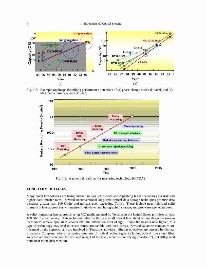
Japanese manufacturers are convinced that over the next decade new emerging applications will pull theperformance of optical storage systems and that evolving conventional optical storage technologies (DVDand MO) are capable of satisfying these demands for at least another seven to eight years (Fig. 1.7).
During the period of the WTEC site visits, PC manufacturers were heavily involved in the advanced R&D of4.7 GB DVD-RAM products. The panel learned that PC manufacturers may combine higher NA optics withshorter wavelength blue lasers and single carrier independent pit edge recording (developed by SONY)together with radial direction partial response (RPR) encoding technique to achieve 15 GB capacity doublelayer disks required for the HDTV standard. Matsushita Electric Company (MEI) will be introducing afrequency doubled blue laser in some of its products within 1999. The panel also learned that MEI wasexperimenting with more transparent PC media layers that enable four-layer disks to be used in highercapacity products. In addition, various mastering techniques including UV laser, SIL lens, e-beam, andprobe mastering are being developed to extend the effective areal density of DVD-ROM products to 50Gb/in2 as described in Fig. 1.8.
All PC manufacturers seem to put highest priority, and therefore significant effort, into achieving backwardand forward compatibility within a product line, and also on compatibility between different product lineswithin the DVD family.
In recent years, MO R&D activity has been revived through the ASMO consortium.
MO drive manufacturers now believe that the MO technology can be extended to 5.2 GB capacity in the nearfuture, and then to 10.4 GB on a 5.25” double-sided disk using 680 nm wavelength and a lens with an NA of0.55. Beyond that, they plan to rely on one of the magnetic super-resolution (MSR) techniques, eitherMagnetic Amplifying Magneto Optical Systems (MAMMOS) from Hitachi-Maxell or Domain WallDisplacement Detection (DWDD) from Canon, in addition to magnetic field modulation, to enable furthercapacity increases. By 2002 they may be able to achieve areal densities approaching 20 Gb/in2 by combiningone of the MSR techniques with the use of a blue laser and larger NA optics. By adopting a format similar toDVD, MO researchers at Fujitsu are contemplating 36 GB capacity disc systems as VCR replacements.Finally, they envision using SIL lenses and parallel heads to extend the areal density and data rate of MOproducts to exceed 100 Gb/in2 and 1 Gb/s respectively.
1. IntroductionOptical Storage8
3rd generation
95 96 97 98 99 00 01 02 03 04
100
50
10
5 DVD-RAM
1st generation2nd generation
4L2L1L
DVD-ROM
Cap
acit
y (G
B)
Year(a)
95 96 97 98 99 00 01 02 03 04 05 0
10050
10
5DVD-RAMC
apac
ity
(GB
)
DVD-ROM
MO-DVD-RAM
3.5”MO
200Gb/in2
20Gb/in2
Terastor
Year(b)
Fig. 1.7. Example roadmaps describing performance potentials of (a) phase change media (Hitachi) and (b)MO media based systems (Fujitsu).
100G
10G
1G1995 2000 2005
UVMastering
Year
Su
rfac
e R
eco
rdin
g D
ensi
ty (
bit
s/in
2 )
2010 2015
1T
10T
E-beammastering
260nmSIL
Mastering
Ultra Large Aperture lenses
High density cuttingphotoresist
Nano-imprinting
ProbeMastering
H-precision injection molding
Ultra smooth substrate
Fig. 1.8. A potential roadmap for mastering technology (OITDA).
LONG TERM OUTLOOK
Many novel technologies are being pursued in parallel towards accomplishing higher capacities per disk andhigher data transfer rates. Several unconventional long-term optical data storage techniques promise datadensities greater than 100 Gb/in2 and perhaps even exceeding Tb/in2. These include near field and solidimmersion lens approaches, volumetric (multi-layer and holographic) storage, and probe storage techniques.
A solid immersion lens approach using MO media pursued by Terastor in the United States promises at least100 Gb/in2 areal density. This technique relies on flying a small optical lens about 50 nm above the storagemedium to achieve spot sizes smaller than the diffraction limit of light. Since the head is now lighter, thistype of technology may lead to access times comparable with hard drives. Several Japanese companies areintrigued by the approach and are involved in Terastor’s activities. Similar objectives are pursued by Quinta,a Seagate Company, where increasing amounts of optical technologies including optical fibers and fiberswitches are used to reduce the size and weight of the head, which is non-flying (“far-field”), but still placedquite near to the disk medium.

Sadik C. Esener 9
Multi-layer (multi-value) storage is pursued both in Japan and the United States. In Japan the effortconcentrates on increasing the number of storage layers in a PC based DVD disk. Some researchers alsoenvision adapting multi-layer recording to MO media by simultaneously reading and computing the data onseveral layers. Both approaches, however, have limited scalability in the number of layers. In the UnitedStates, Call/Recall, Inc. is using a fluorescent disk medium to record and read hundreds of layers. Also in theUnited States, significant effort is being put into developing holographic storage, aiming for areal densitiesexceeding 100 Gb/in2. Companies both in the United States and Japan are exploring the use of parallel headsto speed up data transfer rates. Finally, both in Japan and in the United States, optically assisted probetechniques are being explored to achieve areal densities beyond a Tb/in2. Fig. 1.9 summarizes the author’sprojections for long-term trends in optical storage.
In summary, a fast growing removable data storage market governed by optical storage has resulted fromsubstantial progress that has been made in optical disk storage techniques. These advances have comethrough a combination of laser wavelength reduction, increases in the objective lens numerical aperture,better ISI and cross-talk management, and coding improvements under the constant pull of new applications.Undoubtedly, emerging applications will pull optical storage techniques to reach new performance levels.There is room for advances in storage capacity, as transitions to blue lasers, near-field optical recording, andmulti-layer systems will occur.
To further report and analyze Japan's potential role in this developing important market, in the followingchapters, we present in more depth the status of optical storage in Japan from a business oriented perspective,and a review of the technologies being developed for the near as well as longer terms.
20102005100 M
100 G
1 G
10 G
1 T
10 T
Eff
ecti
ve R
eco
rdin
g D
ensi
ty (
bit
s/in
2 )
magneticrecording
TeraStorplan
Probe Storage
Holographic
DVDplan
2-Photon Multi-layer250-500L
ASMOplan
2000Year
Fig. 1.9. Alternative optical storage technologies and their potential impact (speculativepersonal projections from the author).

1. IntroductionOptical Storage10
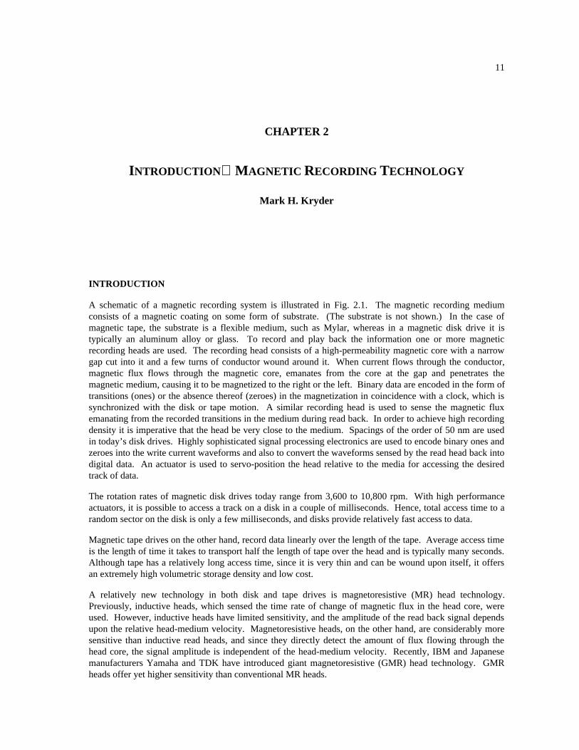
11
CHAPTER 2
INTRODUCTIONMAGNETIC RECORDING TECHNOLOGY
Mark H. Kryder
INTRODUCTION
A schematic of a magnetic recording system is illustrated in Fig. 2.1. The magnetic recording mediumconsists of a magnetic coating on some form of substrate. (The substrate is not shown.) In the case ofmagnetic tape, the substrate is a flexible medium, such as Mylar, whereas in a magnetic disk drive it istypically an aluminum alloy or glass. To record and play back the information one or more magneticrecording heads are used. The recording head consists of a high-permeability magnetic core with a narrowgap cut into it and a few turns of conductor wound around it. When current flows through the conductor,magnetic flux flows through the magnetic core, emanates from the core at the gap and penetrates themagnetic medium, causing it to be magnetized to the right or the left. Binary data are encoded in the form oftransitions (ones) or the absence thereof (zeroes) in the magnetization in coincidence with a clock, which issynchronized with the disk or tape motion. A similar recording head is used to sense the magnetic fluxemanating from the recorded transitions in the medium during read back. In order to achieve high recordingdensity it is imperative that the head be very close to the medium. Spacings of the order of 50 nm are usedin today’s disk drives. Highly sophisticated signal processing electronics are used to encode binary ones andzeroes into the write current waveforms and also to convert the waveforms sensed by the read head back intodigital data. An actuator is used to servo-position the head relative to the media for accessing the desiredtrack of data.
The rotation rates of magnetic disk drives today range from 3,600 to 10,800 rpm. With high performanceactuators, it is possible to access a track on a disk in a couple of milliseconds. Hence, total access time to arandom sector on the disk is only a few milliseconds, and disks provide relatively fast access to data.
Magnetic tape drives on the other hand, record data linearly over the length of the tape. Average access timeis the length of time it takes to transport half the length of tape over the head and is typically many seconds.Although tape has a relatively long access time, since it is very thin and can be wound upon itself, it offersan extremely high volumetric storage density and low cost.
A relatively new technology in both disk and tape drives is magnetoresistive (MR) head technology.Previously, inductive heads, which sensed the time rate of change of magnetic flux in the head core, wereused. However, inductive heads have limited sensitivity, and the amplitude of the read back signal dependsupon the relative head-medium velocity. Magnetoresistive heads, on the other hand, are considerably moresensitive than inductive read heads, and since they directly detect the amount of flux flowing through thehead core, the signal amplitude is independent of the head-medium velocity. Recently, IBM and Japanesemanufacturers Yamaha and TDK have introduced giant magnetoresistive (GMR) head technology. GMRheads offer yet higher sensitivity than conventional MR heads.
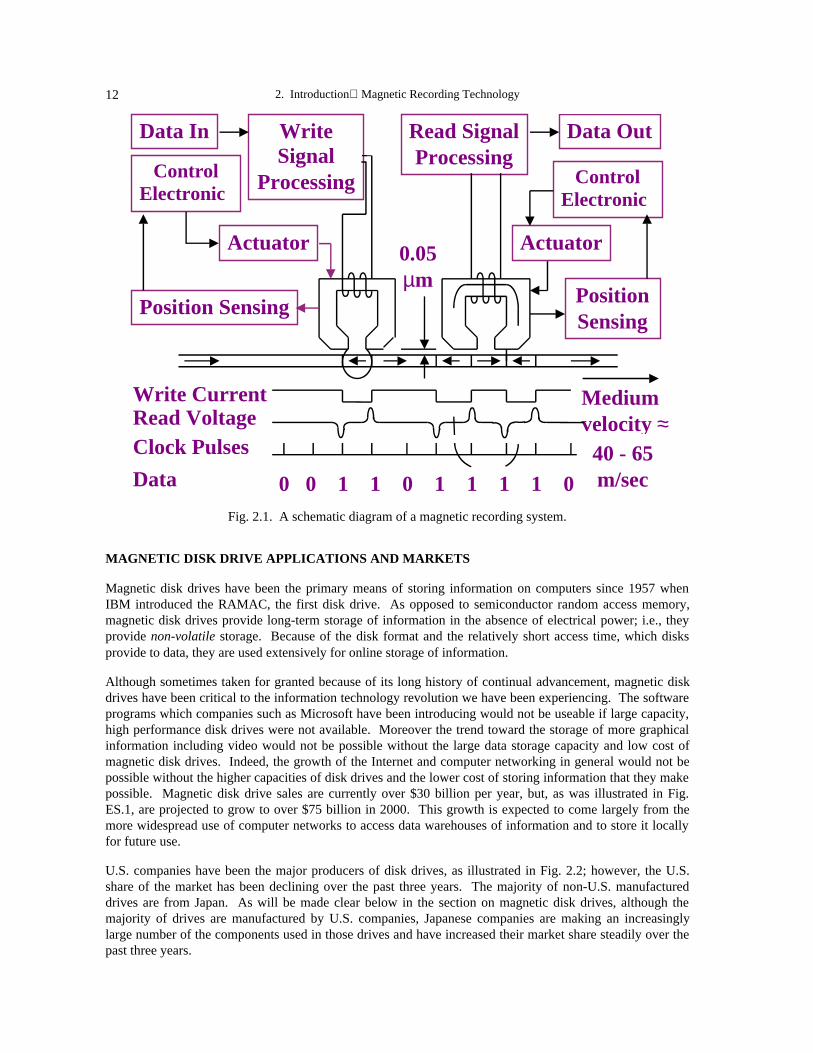
2. IntroductionMagnetic Recording Technology12
Data 0 0 1 1 0 1 1 1 1 0
Clock PulsesRead VoltageWrite Current
Data In WriteSignal
ProcessingControlElectronic
Actuator
Position Sensing
Data OutRead SignalProcessing
Actuator
PositionSensing
ControlElectronic
Mediumvelocity ≈
40 - 65m/sec
0.05µm
Fig. 2.1. A schematic diagram of a magnetic recording system.
MAGNETIC DISK DRIVE APPLICATIONS AND MARKETS
Magnetic disk drives have been the primary means of storing information on computers since 1957 whenIBM introduced the RAMAC, the first disk drive. As opposed to semiconductor random access memory,magnetic disk drives provide long-term storage of information in the absence of electrical power; i.e., theyprovide non-volatile storage. Because of the disk format and the relatively short access time, which disksprovide to data, they are used extensively for online storage of information.
Although sometimes taken for granted because of its long history of continual advancement, magnetic diskdrives have been critical to the information technology revolution we have been experiencing. The softwareprograms which companies such as Microsoft have been introducing would not be useable if large capacity,high performance disk drives were not available. Moreover the trend toward the storage of more graphicalinformation including video would not be possible without the large data storage capacity and low cost ofmagnetic disk drives. Indeed, the growth of the Internet and computer networking in general would not bepossible without the higher capacities of disk drives and the lower cost of storing information that they makepossible. Magnetic disk drive sales are currently over $30 billion per year, but, as was illustrated in Fig.ES.1, are projected to grow to over $75 billion in 2000. This growth is expected to come largely from themore widespread use of computer networks to access data warehouses of information and to store it locallyfor future use.
U.S. companies have been the major producers of disk drives, as illustrated in Fig. 2.2; however, the U.S.share of the market has been declining over the past three years. The majority of non-U.S. manufactureddrives are from Japan. As will be made clear below in the section on magnetic disk drives, although themajority of drives are manufactured by U.S. companies, Japanese companies are making an increasinglylarge number of the components used in those drives and have increased their market share steadily over thepast three years.

Mark H. Kryder 13
1994 1995 1996 19970
20
40
60
80
100
U.S.
Non-U.S.
Year
MarketShare(%)
Fig. 2.2. A bar graph showing the market share of non-U.S. and U.S. manufacturers of disk drives(Disk/Trend).
MAGNETIC DISK DRIVE TECHNOLOGY STATUS
About a decade ago, the areal storage density on magnetic disk drives was advancing at a pace of about 25%per year. At that time semiconductor dynamic random access memory was advancing at a pace of about40% per year, and many semiconductor proponents argued that the time would come when semiconductordevices offered a higher storage density and lower cost than magnetic disk storage. These proponentsargued that with their faster access time, semiconductor devices would replace disk drives. In 1991,however, the magnetic disk drive industry responded by advancing the rate of progress in areal density to60% per year, as illustrated in Fig. 2.3. With the recent announcement of recording at 10 Gb/in2 density byIBM, it is now believed that this rate of progress can be sustained at least into the next millenium. Hence,rather than converging toward the areal density of magnetic disk drives, the areal density of semiconductormemory devices is falling further behind that of magnetic disk drives, and it no longer appears likely thatsemiconductor memory devices will be a significant threat to magnetic storage.

2. IntroductionMagnetic Recording Technology14
Fig. 2.3. Areal density of magnetic hard disk drives and of dynamic random access memories as afunction of the year of shipment (IBM).
In spite of the current rapid pace of advancement in disk drive technology, there are some obstacles toprogress on the future horizon. Since 1957 when IBM introduced the first disk drive, the RAMAC, the arealdensity of magnetic disk recording has been increased over 2 million times by linear scaling of dimensionsof the head, medium and head-medium spacing, while the sensitivity of read heads has been increased.While doing this, it has been necessary to reduce the size of the magnetic particles of which the medium ismade in order to maintain the signal to noise ratio of the system. This is because the signal to noise ratioscales approximately with the number of magnetic particles contained within a bit. If this trend is continued,it is inevitable that the particle size will become so small that the magnetic energy of a particle, KUV, (whereKU is the magnetic anisotropy energy holding the magnetization in its orientation and V is the volume of theparticle) will decrease to values that approach thermal energy given by KBT (where KB is Boltzmann’sconstant and T is the absolute temperature). When this occurs, thermal energy alone may cause magneticrecordings to become unstable.
Although this thermal instability problem appears at first glance to be a problem in the magnetic recordingmedium, in reality part of the limitation comes from the magnetic recording head. Magnetic materials thathave higher values of magnetic anisotropy energy KU exist; however, they require higher fields for recordingthan can be produced with existing recording heads. Before the field produced by the head is made largeenough to write on the medium, the magnetic material from which the head is made saturates.
Modeling has indicated that if magnetic recording continues to be scaled linearly, this thermal instabilitylimit will be reached at about 36 Gb/in2, or a factor of nine higher than the highest density disk drive madetoday. At the 60%/year growth rate, this density would be reached in about five years. However, modeling
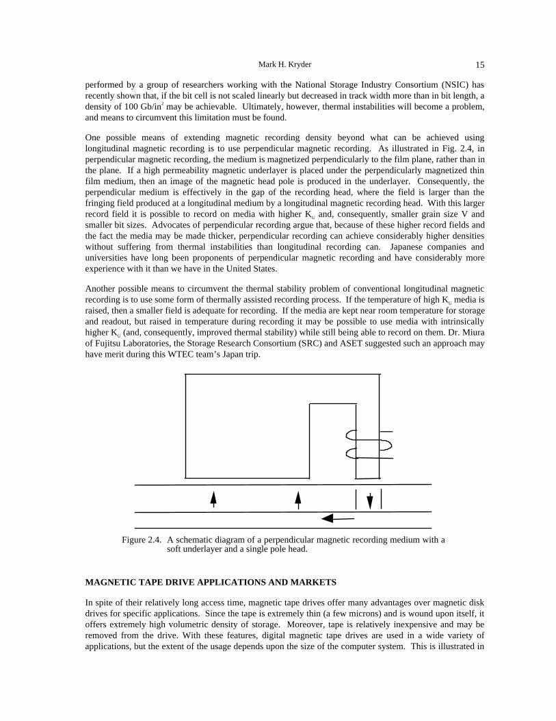
Mark H. Kryder 15
performed by a group of researchers working with the National Storage Industry Consortium (NSIC) hasrecently shown that, if the bit cell is not scaled linearly but decreased in track width more than in bit length, adensity of 100 Gb/in2 may be achievable. Ultimately, however, thermal instabilities will become a problem,and means to circumvent this limitation must be found.
One possible means of extending magnetic recording density beyond what can be achieved usinglongitudinal magnetic recording is to use perpendicular magnetic recording. As illustrated in Fig. 2.4, inperpendicular magnetic recording, the medium is magnetized perpendicularly to the film plane, rather than inthe plane. If a high permeability magnetic underlayer is placed under the perpendicularly magnetized thinfilm medium, then an image of the magnetic head pole is produced in the underlayer. Consequently, theperpendicular medium is effectively in the gap of the recording head, where the field is larger than thefringing field produced at a longitudinal medium by a longitudinal magnetic recording head. With this largerrecord field it is possible to record on media with higher KU and, consequently, smaller grain size V andsmaller bit sizes. Advocates of perpendicular recording argue that, because of these higher record fields andthe fact the media may be made thicker, perpendicular recording can achieve considerably higher densitieswithout suffering from thermal instabilities than longitudinal recording can. Japanese companies anduniversities have long been proponents of perpendicular magnetic recording and have considerably moreexperience with it than we have in the United States.
Another possible means to circumvent the thermal stability problem of conventional longitudinal magneticrecording is to use some form of thermally assisted recording process. If the temperature of high KU media israised, then a smaller field is adequate for recording. If the media are kept near room temperature for storageand readout, but raised in temperature during recording it may be possible to use media with intrinsicallyhigher KU (and, consequently, improved thermal stability) while still being able to record on them. Dr. Miuraof Fujitsu Laboratories, the Storage Research Consortium (SRC) and ASET suggested such an approach mayhave merit during this WTEC team’s Japan trip.
Figure 2.4. A schematic diagram of a perpendicular magnetic recording medium with asoft underlayer and a single pole head.
MAGNETIC TAPE DRIVE APPLICATIONS AND MARKETS
In spite of their relatively long access time, magnetic tape drives offer many advantages over magnetic diskdrives for specific applications. Since the tape is extremely thin (a few microns) and is wound upon itself, itoffers extremely high volumetric density of storage. Moreover, tape is relatively inexpensive and may beremoved from the drive. With these features, digital magnetic tape drives are used in a wide variety ofapplications, but the extent of the usage depends upon the size of the computer system. This is illustrated in

2. IntroductionMagnetic Recording Technology16
Fig. 2.5 where the various applications for digital magnetic tape are shown across the top, and the computersystems they are used in are shown down the side. This figure clearly illustrates that the largest number oftape applications are in large computer systems and that magnetic tape serves a large variety of needs.
The markets for various digital tape drives are shown in Table 2.1. Compact tape drives are small formfactor drives, which are typically used for disk backup on personal computers as well as on a network.Performance tape drives are high-end tape products used predominantly for large computer systems. Tapelibraries are automated media changing subsystems comprised of multiple tape drives, shelves or racks tocontain media, and mechanisms to move media between drives and storage shelves. Summed together thetotal digital tape drive market was about $4.6 billion in 1996.
The market share of non-U.S. and U.S. manufacturers of the various classes of tape drives are also shown inTable 2.1. As in the case of disk drives, U.S. companies sell the majority of digital magnetic tape drivesused for data storage and most of the non-U.S. manufacturers are Japanese. Although Japanese companieshave only a small fraction of the market for magnetic tape drives for data storage, they dominate the analogaudio- and videotape drive businesses. Moreover, they are the dominant manufacturers of magnetic tapemedia.
Fig. 2.5. User application segments for magnetic tape. The inverted triangle shows the tapeapplications (across the top) and the systems use of these applications down the side.The presence of an application with a particular system shows the importance of tapestorage in that environment. (Reprinted with permission of the National StorageIndustry Consortium.)
Table 2.11996 Revenues from Tape Drive Sales
U.S. Mfrs. Non-U.S. Mfrs.
($ million) % ($ million) %
Worldwide
Compact Tape Devices 1,559.8 81.6 350.6 18.4 1,910.4
Performance Tape Drives 988.1 75.6 318.7 24.4 1,306.8
Tape Libraries 1,196.5 85.0 211.3 15.0 1,407.7
TOTAL 3,744.3 81.0 880.6 19.0 4,624.9
Source: Freeman Reports
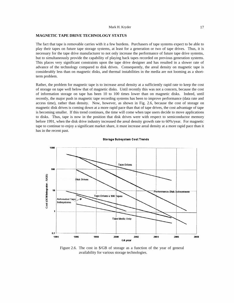
Mark H. Kryder 17
MAGNETIC TAPE DRIVE TECHNOLOGY STATUS
The fact that tape is removable carries with it a few burdens. Purchasers of tape systems expect to be able toplay their tapes on future tape storage systems, at least for a generation or two of tape drives. Thus, it isnecessary for the tape drive manufacturer to not only increase the performance of future tape drive systems,but to simultaneously provide the capability of playing back tapes recorded on previous generation systems.This places very significant constraints upon the tape drive designer and has resulted in a slower rate ofadvance of the technology compared to disk drives. Consequently, the areal density on magnetic tape isconsiderably less than on magnetic disks, and thermal instabilities in the media are not looming as a short-term problem.
Rather, the problem for magnetic tape is to increase areal density at a sufficiently rapid rate to keep the costof storage on tape well below that of magnetic disks. Until recently this was not a concern, because the costof information storage on tape has been 10 to 100 times lower than on magnetic disks. Indeed, untilrecently, the major push in magnetic tape recording systems has been to improve performance (data rate andaccess time), rather than density. Now, however, as shown in Fig. 2.6, because the cost of storage onmagnetic disk drives is coming down at a more rapid pace than that of tape drives, the cost advantage of tapeis becoming smaller. If this trend continues, the time will come when tape users decide to move applicationsto disks. Thus, tape is now in the position that disk drives were with respect to semiconductor memorybefore 1991, when the disk drive industry increased the areal density growth rate to 60%/year. For magnetictape to continue to enjoy a significant market share, it must increase areal density at a more rapid pace than ithas in the recent past.
Figure 2.6. The cost in $/GB of storage as a function of the year of generalavailability for various storage technologies.

2. IntroductionMagnetic Recording Technology18
REFERENCES
Charap, S.H., Pu-Ling Lu and Yanjun He. 1997. Thermal stability of recorded information at high densities. IEEETrans. Magnet., MAG-33, 978.

19
CHAPTER 3
MAGNETIC DISK TECHNOLOGIES
David A. Thompson
INTRODUCTION
Magnetic hard disk technology is the undisputed leader for online storage applications, i.e., for storing datainexpensively, but in such a way as to be available within a time period less than human response times.Although the time delay for the first data bit to become available is thousands of times longer than forsemiconductor memory, the data (when it does arrive) streams from the disk at tens of megabytes persecond. The cost of hard disk storage is a few cents per megabyte, which is several orders of magnitude lessthan for semiconductor memory.
Tape storage is cheaper than disk storage, but its access time is much longer. It is possible to configureoptical storage for online applications, but such a system is inferior to hard disk storage in every respect:cost, data rate, access time, etc. Only by moving to a library configuration or a data interchange application,which both utilize the removability of optical media at the expense of access time and mechanicalcomplexity, does optical storage find a successful niche in which it can compete. There is at this time notechnology that appears to have a chance of displacing hard disk storage in the next 10 years.
One major difference between hard disk and interchange media like tape and disk is the effect that standardsand the need for backward compatibility have on the rate of technological progress. Hard disk standardsinvolve external attributes of the drive only: physical size, power, cooling, and the data bus protocol andconnector. There is no need for the customer to know what technology is being used to store and retrievedata within the box.
The situation with interchange media is different. The customer is vitally interested in his ability to read oldformats and share media with other customers. There is also a benefit from utilizing standards from theaudio and video entertainment industries. As a result, almost all of the tape media progress is spill-over fromthe much larger entertainment market, and many of the optical storage standards are based on compatibilitywith audio or video players.

3. Magnetic Disk Technologies20
This difference is also reflected in the nationality of the companies that manufacture disk drives. As recentlyas 1997, U.S.-based companies produced about 80% of the revenues and an even greater fraction of the harddisk drive (HDD) units sold. This is just the opposite of the situation in tape and optical storage, whereJapanese and other Asian companies dominate the business for both entertainment and for computer storagedevices (see Fig. 3.1 and Tables 3.1-3.3).
Fig. 3.1. U.S. and non-U.S. HDD market share per year (ASET/SRC, Miura, March 1998).
From this data, one might expect that Japan is not a center of HDD technology. This impression iscompletely false! Consider the following observations:
• The most profitable and fastest growing segment of the HDD business is the 2.5-inch laptop drive. It isalso the portion of the business where areal density leadership is most important, since size and powerconsumption are more important in this application than is price per MB. All of the current 2.5-inchdrives are designed in Japan. (This includes IBM’s Fujisawa Laboratory.)
• According to Mark Geenen of TrendFocus (in a lecture on June 23, 1998), the fastest growingcompanies in the HDD business and in the components business (heads, disks) are Japanese. Hitachiand Fujitsu are especially strong in their base technologies, and TDK, Alps, and Yamaha are greatlyincreasing their market share in the head business. A shakeout due to overcapacity in the disk businesswill favor well-financed companies, which include some of the Japanese companies. Overall, it appearsthat Japan’s share of the HDD business is poised to greatly increase in the next few years.
• The approach of the superparamagnetic limit may put an extra emphasis on technological means tochange the evolutionary approach. The panel saw in this study that the larger Japanese companies havea strong advanced technology position in devices, materials, and recording physics.
Other examples of a rising Japanese presence can be seen by a few months of press clippings (Table 3.4), bythe order in which companies have brought magneto resistive (MR) heads to the marketplace (Table 3.5),and in the areal density being shipped as of May 1997 (Table 3.6).

David A. Thompson 21
Table 3.1Share of HDD Market by National Origin, 1995
United States Japan Other U.S. Share(%)
HDD Revenue($ million)
$22,722 $3,610 $250 85.5
HDD Units (million) 79.5 8.4 2 88.4
Source: Gourevitch et al. 1997
Table 3.2Location of HDD Final Assembly, 1995 (% of units)
United States Southeast Asia Japan Other-Asia
Europe Total
4.6 64.2 15.5 5.7 10.0 100
Source: Gourevitch et al. 1997
Table 3.3Geographic Distribution of the Wage Bill (%)
United States Japan S.E. Asia Europe Other
Percent of Total 42.2 23.9 12.9 6.2 14.8
Source: Gourevitch et al. 1997
Table 3.4Recent HeadlinesTypical Press Clippings
Date Headline
5/18/98 Hitachi to Begin Mass-producing GMR Heads
5/13/98 Hitachi Announces a 6.48 GB GMR Mobile HDD
5/12/98 Toshiba Formally Announces a 6.4 GB GMR Mobile Drive
4/18/98 HITACHI Announces 3.5”, Half-High, 12000 rpm 9.1 GB Hard Disk Drive
4/15/98 Fujitsu Introduces Three New Mobile Hard Drives
3/06/98 Integral files for Bankruptcy
2/27/98 HITACHI Reveals New HDAs
2/04/98 Mitsumi Electric to Enter the Magneto-Resistive (MR) Head Race
2/03/98 Fujitsu to Incorporate GMR Head Technology in Disk Drives
1/23/98 HITACHI Announces 12,000 rpm High-End hard Disk Drive
1/22/98 Seagate Exits the Mobile HDD Business
1/20/98 Hitachi Announces New 2.5” Mobile Hard Disk Drives
5/13/98 Hitachi Metals to Sample GMR Heads in February
The connection between the HDD industry and the Japanese universities has been weak for many years, butthe recent establishment of the Storage Research Consortium (SRC) has begun the process of building thesort of ties in Japan that exist in the United States and Singapore.
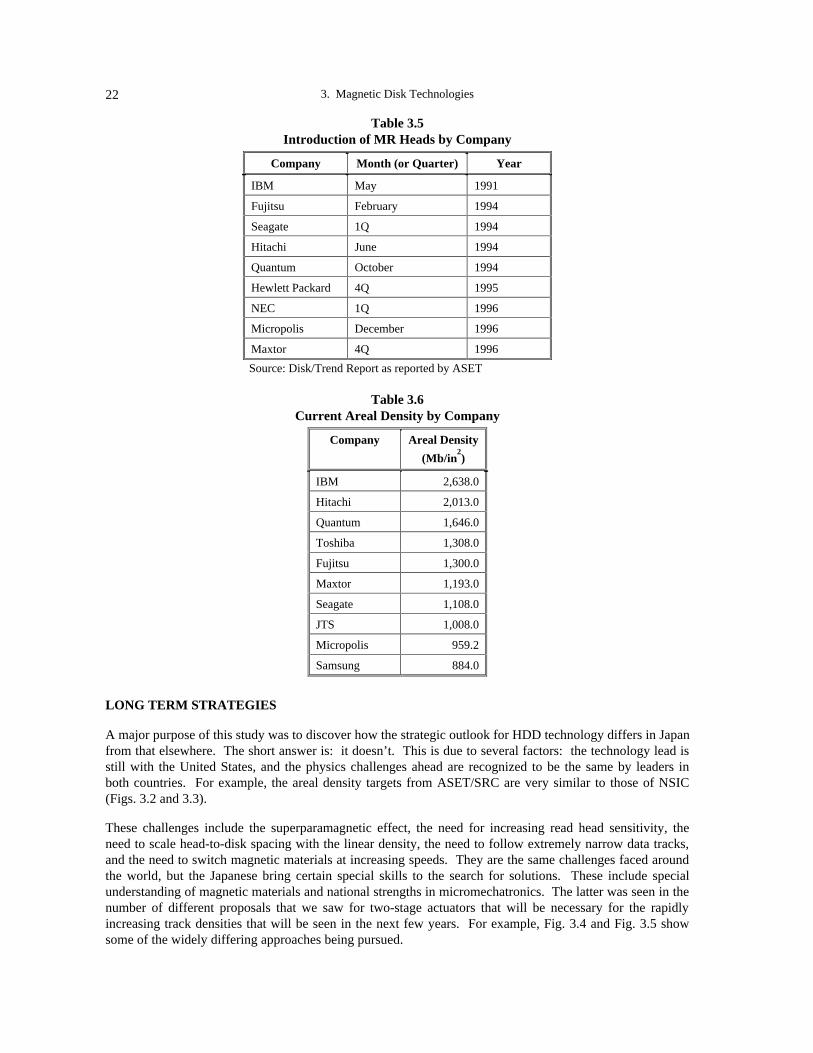
3. Magnetic Disk Technologies22
Table 3.5Introduction of MR Heads by Company
Company Month (or Quarter) Year
IBM May 1991
Fujitsu February 1994
Seagate 1Q 1994
Hitachi June 1994
Quantum October 1994
Hewlett Packard 4Q 1995
NEC 1Q 1996
Micropolis December 1996
Maxtor 4Q 1996
Source: Disk/Trend Report as reported by ASET
Table 3.6Current Areal Density by Company
Company Areal Density
(Mb/in2)
IBM 2,638.0
Hitachi 2,013.0
Quantum 1,646.0
Toshiba 1,308.0
Fujitsu 1,300.0
Maxtor 1,193.0
Seagate 1,108.0
JTS 1,008.0
Micropolis 959.2
Samsung 884.0
LONG TERM STRATEGIES
A major purpose of this study was to discover how the strategic outlook for HDD technology differs in Japanfrom that elsewhere. The short answer is: it doesn’t. This is due to several factors: the technology lead isstill with the United States, and the physics challenges ahead are recognized to be the same by leaders inboth countries. For example, the areal density targets from ASET/SRC are very similar to those of NSIC(Figs. 3.2 and 3.3).
These challenges include the superparamagnetic effect, the need for increasing read head sensitivity, theneed to scale head-to-disk spacing with the linear density, the need to follow extremely narrow data tracks,and the need to switch magnetic materials at increasing speeds. They are the same challenges faced aroundthe world, but the Japanese bring certain special skills to the search for solutions. These include specialunderstanding of magnetic materials and national strengths in micromechatronics. The latter was seen in thenumber of different proposals that we saw for two-stage actuators that will be necessary for the rapidlyincreasing track densities that will be seen in the next few years. For example, Fig. 3.4 and Fig. 3.5 showsome of the widely differing approaches being pursued.

David A. Thompson 23
Fig. 3.2. Roadmap (IBM).
Fig. 3.3. ASET/SRC areal density projection (Miura, March 1998).

3. Magnetic Disk Technologies24
Fig. 3.4. Possible microactuator designs (Miura, March 1998).
Fig. 3.5. TDK microactuator (described at TMRC, August 1998).
The ASET presentation at the March 1998 WTEC workshop in Tokyo contains a succinct summary of someof the materials work that the panel saw. Japan’s leadership in magnetic materials predates the disk drivebusiness and reflects its prowess in solid state physics, in high tech fabrication methods, and the benefits ofbeing the leader in magnetic recording for audio and video applications. Figs. 3.6 through 3.8 show aportion of that summary.
An alternative form of magnetic recording called “perpendicular recording” has been an almost exclusivelyJapanese domain for 20 years (Fig. 3.9). Until recently it had no particular advantages over conventionalrecording, but as one begins to see superparamagnetic effects limiting areal density, perpendicular mediahold the promise of being more stable than longitudinal media for the same number of grains per bit. This isprimarily because perpendicular media are thicker for the same areal density than longitudinal media (whichallows more stored energy per grain); because the demagnetizing fields in perpendicular recording favorhigh bit densities (the opposite of the longitudinal case); and because the strength of the field from the writehead can be stronger for perpendicular recording. If this turns out to be true, then Japan has a substantiallead in gaining experience with this technology.
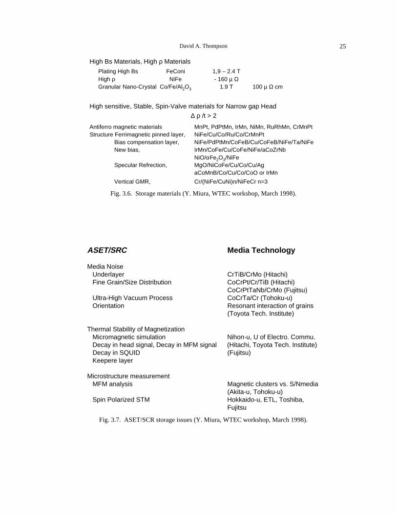
David A. Thompson 25
High Bs Materials, High ρ Materials
Plating High Bs FeConi 1,9 – 2.4 T High ρ NiFe - 160 µ Ω
Granular Nano-Crystal Co/Fe/Al2O3 1.9 T 100 µ Ω cm
High sensitive, Stable, Spin-Valve materials for Narrow gap Head
∆ ρ /t > 2
Antiferro magnetic materials MnPt, PdPtMn, IrMn, NiMn, RuRhMn, CrMnPtStructure Ferrimagnetic pinned layer, NiFe/Cu/Co/Ru/Co/CrMnPt
Bias compensation layer, NiFe/PdPtMn/CoFeB/Cu/CoFeB/NiFe/Ta/NiFeNew bias, IrMn/CoFe/Cu/CoFe/NiFe/aCoZrNb
NiO/αFe2O3/NiFeSpecular Refrection, MgO/NiCoFe/Cu/Co/Cu/Ag
aCoMnB/Co/Cu/Co/CoO or IrMn
Vertical GMR, Cr/(NiFe/CuNi)n/NiFeCr n=3
Fig. 3.6. Storage materials (Y. Miura, WTEC workshop, March 1998).
ASET/SRC Media Technology
Media Noise Underlayer CrTiB/CrMo (Hitachi) Fine Grain/Size Distribution CoCrPt/Cr/TiB (Hitachi) CoCrPtTaNb/CrMo (Fujitsu) Ultra-High Vacuum Process CoCrTa/Cr (Tohoku-u) Orientation Resonant interaction of grains (Toyota Tech. Institute)
Thermal Stability of Magnetization Micromagnetic simulation Nihon-u, U of Electro. Commu. Decay in head signal, Decay in MFM signal (Hitachi, Toyota Tech. Institute) Decay in SQUID (Fujitsu) Keepere layer
Microstructure measurement MFM analysis Magnetic clusters vs. S/Nmedia (Akita-u, Tohoku-u) Spin Polarized STM Hokkaido-u, ETL, Toshiba, Fujitsu
Fig. 3.7. ASET/SCR storage issues (Y. Miura, WTEC workshop, March 1998).
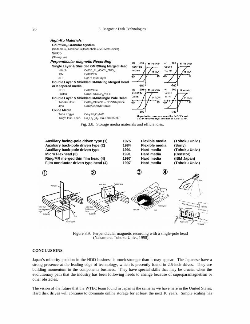
3. Magnetic Disk Technologies26
High-Ku MaterialsCoPt/SiO2 Granular System(Saitama-u, Toshiba/Fujitsu/Tohoku/JVC/Matsushita)
SmCo(Shinsyu-u)
Perpendicular magnetic RecordingSingle Layer & Shielded GMR/Ring Merged Head
Hitach CoCr19Pt10/CoCr35/TiCr10
IBM CoCrPt/TiAIT Co/Pd multi layer
Double Layer & Shielded GMR/Ring Merged Heador Keepered media
NEC CoCr/NiFeFujitsu CoCrTa/CoCr35/NiFe
Double Layer & Shielded GMR/Single Pole HeadTohoku Univ. CoCr23/NiFeNb – CoZrNb probeJVC CoCr/CoZrNb/SmCo
Oxide MediaToda Kogyo Co-γ Fe2O3/NiOTokyo Insti. Tech. CoxFe3-xO4, Ba-Ferrite/ZnO
Fig. 3.8. Storage media materials and efficiencies.
Auxiliary facing-pole driven type (1) 1975 Flexible media (Tohoku Univ.)Auxiliary back-pole driven type (2) 1984 Flexible media (Sony)Auxiliary back-pole driven type 1991 Hard media (Tohoku Univ.)Micro Flexhead (3) 1991 Hard media (Censtor)Ring/MR merged thin film head (4) 1997 Hard media (IBM Japan)Film conductor driven type head (4) 1997 Hard media (Tohoku Univ.)
Figure 3.9. Perpendicular magnetic recording with a single-pole head(Nakamura, Tohoku Univ., 1998).
CONCLUSIONS
Japan’s minority position in the HDD business is much stronger than it may appear. The Japanese have astrong presence at the leading edge of technology, which is presently found in 2.5-inch drives. They arebuilding momentum in the components business. They have special skills that may be crucial when theevolutionary path that the industry has been following needs to change because of superparamagnetism orother obstacles.
The vision of the future that the WTEC team found in Japan is the same as we have here in the United States.Hard disk drives will continue to dominate online storage for at least the next 10 years. Simple scaling has
David A. Thompson 27
driven the technology for 40 years. In that time, the MR head represents the only change in the physics ofhow a disk drive operates. But 10 years from now, other significant changes in technology will benecessary; simple scaling of the storage medium will not be possible. At that time, the leading companieswill have had to grapple with a number of technical challenges, for which the Japanese are well prepared.
REFERENCES
Gourevitch, Peter, et al. 1997. WHO IS US? The nationality of production in the hard disk industry. Report 97-01,UCSD, March (See http://www-irps.ucsd.edu/~sloan/papers/whoisus.htm/#toc21).
Miura, Y., 1998. Presentation at the U.S. – Japan Workshop on Future Data Storage Technologies, Tokyo, Japan,March 9.

3. Magnetic Disk Technologies28

29
CHAPTER 4
MAGNETIC TAPE STORAGE
William D. Doyle
BACKGROUND
The information contained in this report originates from three principle sources: (1) participation in therecent tape technology roadmap program conducted by the National Storage Industry Consortium(NSIC)1,.(2) WTEC-sponsored visits to several Japanese companies including Sony, Fuji Film andMatsushita, which have a particular interest in magnetic tape, (3) contacts with JVC in Japan and Quantegyand Imation in the United States.
Magnetic tape is the oldest technology in the current storage hierarchy. It has dominated program storageand data backup in large computer systems for about 50 years, the audio market (Philips cassette) for 20years (until the development of the CD) and the video market (VHS) for 20 years. However, the latter isthreatened in the future by optical DVD. The reason for the longevity of tape in data storage is simply that ithas provided the lowest cost solution for the required performance. Heads and media developed for theconsumer market were incorporated into storage systems with relatively small additional effort and, becauseof the volume and price sensitivity of the consumer market, at relatively low cost.
The cost per gigabyte of various actual and projected storage technologies is shown as a function of time inFig. 4.1. Traditionally, tape enjoyed a cost advantage relative to disk of two orders of magnitude, but, as thecost trend shows, this has narrowed rapidly to an order of magnitude in 1998 with a projected crossoverpoint in less than 10 years. This is happening primarily because of the extraordinary 60%/year rate ofincrease in disk storage density resulting in similar decreases in cost. Tape is threatened, not by opticaltechnology, but by disk technology unless it can sharply increase storage density at a rate comparable todisks.
Tape is a removable medium, and, consequently advances are hindered by the requirement forinterchangeability, backward compatibility and agreement on specifications. There are also many formatswith different tape widths and cartridge designs, which defocus development efforts. Fortunately, the majormarket in the future will be large and medium size systems where the number of formats is limited. Theprevious demand for small, low cost tape systems for data back-up in PCs, which was served by severalformats, will be satisfied by optical disk or even extra hard drives. Despite these hurdles, rapid progressmust be achieved, and the technology barriers to achieving it are highlighted here. Particular attention is
1 NSIC. The National Storage Industry Consortium (NSIC)’s Tape Technology Roadmap is available from NSIC, 9888Carroll Center Road, Suite 115, San Diego, CA 92126-4580.
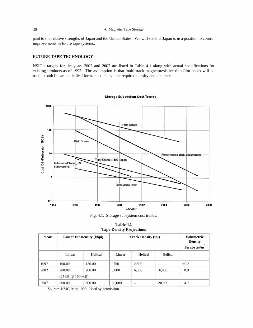
4. Magnetic Tape Storage30
paid to the relative strengths of Japan and the United States. We will see that Japan is in a position to controlimprovements in future tape systems.
FUTURE TAPE TECHNOLOGY
NSIC’s targets for the years 2002 and 2007 are listed in Table 4.1 along with actual specifications forexisting products as of 1997. The assumption is that multi-track magnetoresistive thin film heads will beused in both linear and helical formats to achieve the required density and data rates.
Fig. 4.1. Storage subsystem cost trends.
Table 4.1Tape Density Projections
Year Linear Bit Density (kbpi) Track Density (tpi) VolumetricDensity
Terabytes/in3
Linear Helical Linear Helical Helical
1997 100.00 120.00 750 2,800 - <0.2
2002 200.00 200.00 6,000 6,000 6,000 0.9
(25 dB @ 100 kcfi)
2007 300.00 300.00 20,000 -- 20,000 4.7
Source: NSIC, May 1998. Used by permission.

William D. Doyle 31
Further, by 2007, both formats will have the same volumetric density of ~5 terabytes/in3. Clearly, the
projections show that most of the improvement, particularly in longitudinal recorders, will come fromsignificantly increased track density. The increases in linear density are not inconsistent with the historicaldata although there has been a flattening-off since approximately 1995. It is also required that the tapethickness be reduced to about 4 µm while still maintaining sufficient mechanical properties to be transportedreliably.
The various components of a tape storage system are shown in Table 4.2 with an indication of the relativeposition of the United States and Japan. Head technology and system electronics will be derived from harddisk drive (HDD) development but new media, improved head/tape tribological properties, reliable tapetransports and new systems must come from the tape industry.
Table 4.2Requirements for 4.7 Terabyte/in3
Requirements World Leader
From HDD Development
- Multi-track GMR heads in both linear and helical systems to achieve medianoise-limited SNR (Sony, Yamaha)*
- Electronics including EPR4 channel combined with (O,K) codes
U.S./Japan
U.S.
From Tape Development
- New media (Fuji Film)*
- Head-media tribology (Sony)*
- Fundamental understanding of tape mechanics and transport (Sony)*
- System development (Sony, Matsushita)*
Japan
Japan
U.S./Japan
U.S./Japan
*WTEC Visits
HEAD TECHNOLOGY
Enormous improvement in read heads for HDDs has been realized by the introduction of magneto resistive(MR) heads in 1991 by IBM and later many others, and more recently in 1998 by the introduction of GMRheads by IBM followed closely by Hitachi. IBM, for many years, also used multi-track MR sensors in acomplex head structure for some tape systems, and recently the quarter inch format adopted multi-track MRthin film heads for advanced products.
Developers of future tape systems will rely primarily on progress in HDD heads for the design andmanufacture of GMR heads. At the present time, IBM is the world leader with Hitachi a close second. Atthe present time, the only independent GMR head supplier is Yamaha, known in the United States primarilyfor its musical instruments. It has been suggested that Yamaha obtained at least some of the basictechnology for GMR from another Japanese company.
There is an enormous effort in GMR both in Japan and the United States with sufficient manufacturingresources in both countries. The capabilities would be rated as equal.
ELECTRONICS
Tape systems will also derive the channel design and read/write electronics from HDDs, incorporating theminto more complex chips required for multi-channel recording. Because of its present lead in HDDs, theUnited States has a significant advantage.
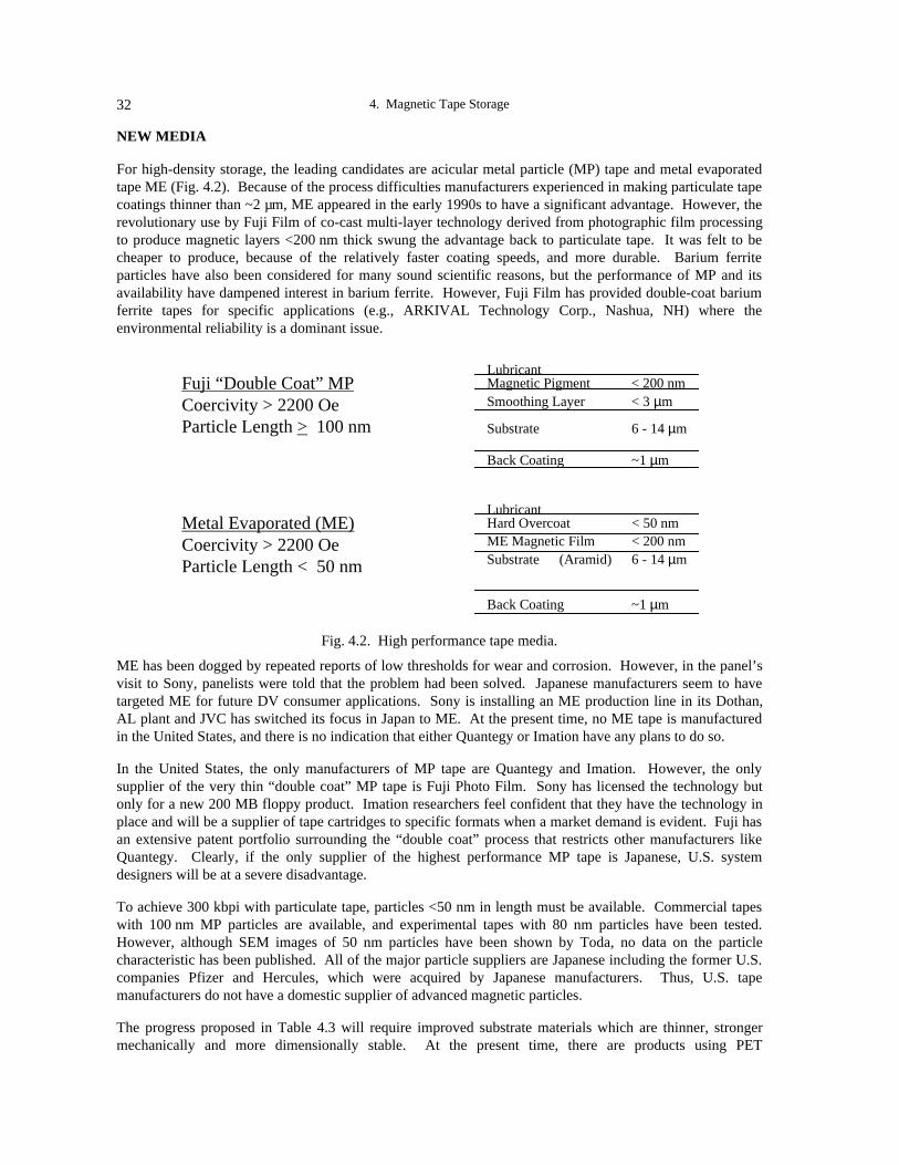
4. Magnetic Tape Storage32
NEW MEDIA
For high-density storage, the leading candidates are acicular metal particle (MP) tape and metal evaporatedtape ME (Fig. 4.2). Because of the process difficulties manufacturers experienced in making particulate tapecoatings thinner than ~2 µm, ME appeared in the early 1990s to have a significant advantage. However, therevolutionary use by Fuji Film of co-cast multi-layer technology derived from photographic film processingto produce magnetic layers <200 nm thick swung the advantage back to particulate tape. It was felt to becheaper to produce, because of the relatively faster coating speeds, and more durable. Barium ferriteparticles have also been considered for many sound scientific reasons, but the performance of MP and itsavailability have dampened interest in barium ferrite. However, Fuji Film has provided double-coat bariumferrite tapes for specific applications (e.g., ARKIVAL Technology Corp., Nashua, NH) where theenvironmental reliability is a dominant issue.
Fuji “Double Coat” MPCoercivity > 2200 OeParticle Length > 100 nm
LubricantMagnetic Pigment < 200 nmSmoothing Layer < 3 µm
Substrate 6 - 14 µm
Back Coating ~1 µm
Metal Evaporated (ME)Coercivity > 2200 OeParticle Length < 50 nm
LubricantHard Overcoat < 50 nmME Magnetic Film < 200 nmSubstrate (Aramid) 6 - 14 µm
Back Coating ~1 µm
Fig. 4.2. High performance tape media.
ME has been dogged by repeated reports of low thresholds for wear and corrosion. However, in the panel’svisit to Sony, panelists were told that the problem had been solved. Japanese manufacturers seem to havetargeted ME for future DV consumer applications. Sony is installing an ME production line in its Dothan,AL plant and JVC has switched its focus in Japan to ME. At the present time, no ME tape is manufacturedin the United States, and there is no indication that either Quantegy or Imation have any plans to do so.
In the United States, the only manufacturers of MP tape are Quantegy and Imation. However, the onlysupplier of the very thin “double coat” MP tape is Fuji Photo Film. Sony has licensed the technology butonly for a new 200 MB floppy product. Imation researchers feel confident that they have the technology inplace and will be a supplier of tape cartridges to specific formats when a market demand is evident. Fuji hasan extensive patent portfolio surrounding the “double coat” process that restricts other manufacturers likeQuantegy. Clearly, if the only supplier of the highest performance MP tape is Japanese, U.S. systemdesigners will be at a severe disadvantage.
To achieve 300 kbpi with particulate tape, particles <50 nm in length must be available. Commercial tapeswith 100 nm MP particles are available, and experimental tapes with 80 nm particles have been tested.However, although SEM images of 50 nm particles have been shown by Toda, no data on the particlecharacteristic has been published. All of the major particle suppliers are Japanese including the former U.S.companies Pfizer and Hercules, which were acquired by Japanese manufacturers. Thus, U.S. tapemanufacturers do not have a domestic supplier of advanced magnetic particles.
The progress proposed in Table 4.3 will require improved substrate materials which are thinner, strongermechanically and more dimensionally stable. At the present time, there are products using PET
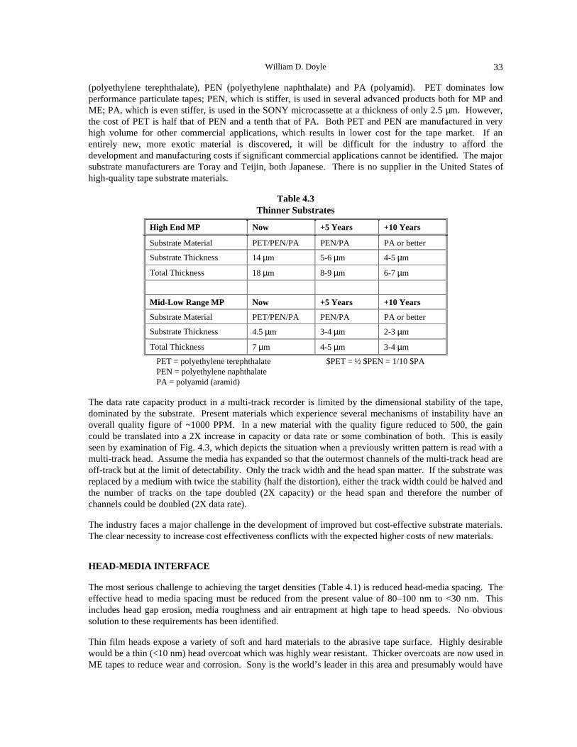
William D. Doyle 33
(polyethylene terephthalate), PEN (polyethylene naphthalate) and PA (polyamid). PET dominates lowperformance particulate tapes; PEN, which is stiffer, is used in several advanced products both for MP andME; PA, which is even stiffer, is used in the SONY microcassette at a thickness of only 2.5 µm. However,the cost of PET is half that of PEN and a tenth that of PA. Both PET and PEN are manufactured in veryhigh volume for other commercial applications, which results in lower cost for the tape market. If anentirely new, more exotic material is discovered, it will be difficult for the industry to afford thedevelopment and manufacturing costs if significant commercial applications cannot be identified. The majorsubstrate manufacturers are Toray and Teijin, both Japanese. There is no supplier in the United States ofhigh-quality tape substrate materials.
Table 4.3Thinner Substrates
High End MP Now +5 Years +10 Years
Substrate Material PET/PEN/PA PEN/PA PA or better
Substrate Thickness 14 µm 5-6 µm 4-5 µm
Total Thickness 18 µm 8-9 µm 6-7 µm
Mid-Low Range MP Now +5 Years +10 Years
Substrate Material PET/PEN/PA PEN/PA PA or better
Substrate Thickness 4.5 µm 3-4 µm 2-3 µm
Total Thickness 7 µm 4-5 µm 3-4 µm
PET = polyethylene terephthalate $PET = ½ $PEN = 1/10 $PAPEN = polyethylene naphthalatePA = polyamid (aramid)
The data rate capacity product in a multi-track recorder is limited by the dimensional stability of the tape,dominated by the substrate. Present materials which experience several mechanisms of instability have anoverall quality figure of ~1000 PPM. In a new material with the quality figure reduced to 500, the gaincould be translated into a 2X increase in capacity or data rate or some combination of both. This is easilyseen by examination of Fig. 4.3, which depicts the situation when a previously written pattern is read with amulti-track head. Assume the media has expanded so that the outermost channels of the multi-track head areoff-track but at the limit of detectability. Only the track width and the head span matter. If the substrate wasreplaced by a medium with twice the stability (half the distortion), either the track width could be halved andthe number of tracks on the tape doubled (2X capacity) or the head span and therefore the number ofchannels could be doubled (2X data rate).
The industry faces a major challenge in the development of improved but cost-effective substrate materials.The clear necessity to increase cost effectiveness conflicts with the expected higher costs of new materials.
HEAD-MEDIA INTERFACE
The most serious challenge to achieving the target densities (Table 4.1) is reduced head-media spacing. Theeffective head to media spacing must be reduced from the present value of 80–100 nm to <30 nm. Thisincludes head gap erosion, media roughness and air entrapment at high tape to head speeds. No obvioussolution to these requirements has been identified.
Thin film heads expose a variety of soft and hard materials to the abrasive tape surface. Highly desirablewould be a thin (<10 nm) head overcoat which was highly wear resistant. Thicker overcoats are now used inME tapes to reduce wear and corrosion. Sony is the world’s leader in this area and presumably would have

4. Magnetic Tape Storage34
knowledge of the efficiency of head overcoats as well. Several U.S. companies, including IBM, Seagate andStorageTek, make tape heads and presumably are studying this problem.
Peak media roughness, not the average roughness, limits the spacing between the head and media. It is nowabout 20 nm and must be reduced by improved processing to <10 nm.
Traditionally, tape heads were made with long throat heights, which wore away during use. This is onereason VCRs eventually fail. Thin film heads have very short throat heights (<1.5 µm) so a more creativesolution must be found. The head slider used in an HDD is a very sophisticated, aerodynamic form designedto keep the head “flying” close to the media surface. Similar analysis must be employed to minimize theflying height of the head over the tape at high tape-head speeds. The United States is in a strong position inthis area because of its leadership in HDDs.
Standard Media
ReadHeads
Read Heads
Previously Recorded TracksSPAN
2X Improvement in Stability− Double the span length (double the data rate) at fixed track width (fixed
capacity)OR
− Halve the track width (double the capacity) at constant span length(constant data rate)
Fig. 4.3. Substrate stability–capacity/data rate trade-offs.
CRITICAL ISSUES
1. Can the United States develop a domestic source for advanced tape media? Unless this occurs, systemdesigners will be limited by the availability of experimental tapes from non-U.S. suppliers and may beforced to adopt particular formats supported by the present U.S. manufacturers. Reduction in thenumber of formats would be better for users but not necessarily as profitable for the manufacturers andwould certainly constrain innovation. The recent agreement between IBM, Seagate and Hewlett-Packard to develop a new linear open format is a very positive step. This area is an excellentopportunity for an ATP (DOC/NIST) award.
2. Is it practical with traditional media and heads to achieve a spacing of 30 nm? This is the most difficulttechnical problem limiting storage density. Novel materials work is required and should be a focus areafor NSF.
3. Does the industry have the resources to fund the development of new substrate materials? Probably notis the answer. An industry-wide materials research program supported by both the United States andJapan would have a major impact.
4. Will the cost of new substrate materials prevent their widespread use? The substrate is a very largefraction of media cost. A factor of 10 higher cost for PA clearly has limited its application.Remembering that tape exists because of its relatively low cost, the industry faces a critical dilemmawhich may make it difficult to achieve the density target (Table 4.1) proposed by NSIC.
35
CHAPTER 5
R&D ACTIVITIES IN OPTICAL DATA STORAGE MEDIA
Masud Mansuripur
INTRODUCTION
During the first week of April 1998, the WTEC panel on future data storage technologies visited theResearch and Development Department of Nikon Corporation at Shinagawa-ku in Tokyo, the CorporateResearch and Development Laboratory of Pioneer Corporation in Tokyo, and the Hypermedia ResearchCenter, Optical Recording Technology Laboratory, of Sanyo Corporation in Gifu prefecture. What followsis a summary of the observations made during these visits and a fairly detailed description of theconversations with scientists, engineers, and technical managers with whom the panel met. To put thesevisits in perspective, the first part of the report gives an overview of the field of optical data storage. All thetechnical terms are defined, and the various methods and technologies of relevance to optical data storage arereviewed.
AN OVERVIEW OF THE FIELD OF OPTICAL DISK DATA STORAGE
Our need for storage is explosive; fueled by multimedia requirement for text, images, video and audio,storage requirements are growing at an exponential rate and are expected to exceed 1020 bits (12 exabytes) inthe year 2000. With an increasing amount of information being generated or captured electronically, a largefraction, perhaps as much as 40%, will be stored digitally. To meet this need, the hierarchy of on-line, near-line and off-line storage systems will be composed of many diverse technologies: magnetic disk drives,magnetic tape drives and tape libraries, optical disk drives and optical libraries. The mix of these sub-systems will be very application-specific so as to optimize the performance and cost of the overall system.
An optical storage system is a particularly attractive component of this hierarchy because it provides dataaccess times that are an intermediate solution between a hard disk drive and a tape drive. Access time is thetime, including latency, required to start retrieving a random block of data and typically ranges from lessthan 10 msec for a hard disk drive, to 30–50 msec for an optical disk drive, and several seconds for a tapedrive. It becomes an important link in the chain as data are staged up and down between cpu, memory, andstorage.
Perhaps the most enabling feature of optical storage is the removability of the storage medium. Withseparations of a few millimeters between the recording surface and the optical 'head', and with active servosfor focusing and tracking, the medium can be removed and replaced with relatively loose tolerances. Theinfamous head crashes often experienced in hard disk drives do not occur in optical drives. Data reliabilityand removability are further enhanced by using the 1.2 mm transparent disk substrate as a protective cover to

5. R&D Activities in Optical Data Storage Media36
keep contamination away from the recording surface. (The recently announced digital versatile disk or DVDwill have a substrate thickness of only 0.6 mm.)
Removability has created a whole new industry in CD-audio. CD-ROMs have enhanced the efficiency ofdistribution and use of software, games, and video. These read-only disks containing 680 MB ofinformation can be mass replicated by injection molding in a few seconds for less than 10¢ each, and theyare virtually indestructible. One-day express mail of 125 CDs is an effective data rate of 1.0 MB/s.
At the other end of the spectrum, phase change and magneto-optical disks are used in WORM (write-once-read-many) and read/write/erase systems where a single disk can contain almost 5 GB. Using robotics,storage libraries can be assembled with capacities of a terabyte with access to any disk in under 5 seconds.
This review will discuss the fundamentals of optical storage, the components that comprise a system, and theemerging technologies that will allow increased performance, higher storage capacities, and lower cost.
Several international conferences on optical data storage are held each year, and the proceedings of theseconferences are a good source of information concerning the latest developments in this field. References(JSAP 1995; OSA 1966; MORIS 1996) provide some information about these conference proceedingsand/or digests. There are also several published books in this area, to which the readers are referred for anin-depth coverage of the various subjects (Bouwhius et al. 1985; Marchant 1990; Mansuripur 1995;McDaniel & Victora 1997).
Optical data storage research in the United States dates back to the late 1950s and early 1960s when BellLabs, IBM, 3M, and Honeywell, among others, developed several key concepts and technologies for opticalrecording. Several important patents were filed in those early days, which eventually became the property ofDisco Vision Associates (DVA), a California-based company with ties to Pioneer of Japan. In recent years,several large U.S. companies (IBM, Eastman Kodak, 3M) have withdrawn from the field of optical storage,either dismantling or selling off their manufacturing facilities in the United States. At the same time a fewsmall companies (MaxOptix, MOST, Laser Byte, Pinnacle Micro), which had carved a niche market forthemselves by bringing innovative designs or assembled products to the market, have either failed or arestruggling to survive. About 2.5 years ago two startup companies (Quinta and TeraStor) began in California,with the express goal of marrying optical and magnetic recording technologies. Although the promisedproducts of Quinta and TeraStor have not yet materialized in the market, their approach has created aresurgence of interest in the field, especially among the hard drive manufacturers, who see this as a potentialthreat, as well as an opportunity to overcome the dreaded “superparamagnetic problem.”
Recording and Readout of Information on Optical Disks
An optical disk is a plastic (or glass) substrate with one or more thin-film layers coated upon its surface(s).The information may be prerecorded on the surface of the substrate by the disk manufacturer, or it may berecorded on one or more of the thin film layers by the user. Typical diameters of presently available opticaldisks are as follows:
• 12 cm, as in compact disk audio (CD), compact disk read-only memory (CD-ROM), compact discrecordable (CD-R), and digital versatile disk (DVD)
• 2.5”, as in digital audio mini disk (MD)
• 3.5”, as in magneto-optical (MO) removable storage devices
• 5.25”, as in both magneto-optical and phase-change (PC) rewritable disks
• 12” and 14”, such as the write-once-read-many (WORM) media manufactured by Kodak and othercompanies for high volume storage applications
In the case of read-only media the information is pressed onto the substrate by injection molding of plastics,or by embossing of a layer of photopolymer coated on a glass substrate (Bouwhuis et al. 1985; Marchant1990). The substrate is then coated with a thin metal layer (e.g., aluminum) to enhance its reflectivity. In

Masud Mansuripur 37
other types of optical disks, some information, such as format marks and grooves, may be stamped onto thesubstrate itself, but then the substrate is coated with a storage layer that can be modified later by the userduring recording of information. Typical storage layers are dye-polymer films for write-once applications,tellurium alloys for ablative recording (also write-once), GeSbTe for phase-change rewritable media, andTbFeCo magnetic films for magneto-optical disks (also rewritable) (Marchant 1990; Mansuripur 1995;McDaniel & Victora 1997).
CD technology was developed jointly by Philips of the Netherlands and Sony of Japan in the late 1970s andearly 1980s, then introduced to the market in 1983 as the hugely successful compact audio disk. Today mostof the research and advanced development work in DVD (the successor to CD) and future generations ofread-only media takes place in Japan. Sony, Matsushita, Pioneer, Toshiba, Sharp, and NEC are some of theleading Japanese companies in this area. The MiniDisc (MD) was pioneered by Sony, and despite a sluggishearly start, has become a very successful product in Japan. The major players in the field of magneto-opticaldata storage are Sony, Fujitsu, Hitachi Maxell, Mitsubishi, Nikon, and Sanyo. In phase-change opticalrecording, the leaders are Matsushita, Toshiba, and NEC, recently joined by Sony. Many other companiesare involved in the development of components (lasers, miniature optics, actuators, detectors, substrates,spindle motors, etc.) as well as mastering machines and test equipment for optical recording products. Theseinclude some of the major multinational corporations as well as smaller firms.
In a typical disk the storage layer is sandwiched between two dielectric layers, and the stack is capped with areflector layer (e.g., aluminum or gold), and protected with a lacquer layer. The dielectric layers and thereflective layer perform several tasks: protecting the storage layer, creating an optically tuned structure thathas optimized reflectivity and/or absorptivity, allowing the tailoring of the thermal properties of the disk forrapid cooling and reduction of thermal cross-talk during writing, and so on (Mansuripur 1995; McDonaldand Victora 1997).
Fig. 5.1 is a schematic diagram showing the basic elements of an optical disk drive. The laser is usually asemiconductor laser diode, whose beam is collimated by a well-corrected lens and directed towards anobjective lens through a beam-splitter. The objective lens focuses the beam onto the disk and collects thereflected light. This reflected light is directed (at the beam-splitter) towards the detectors, which produce adata readout signal as well as servo signals for automatic focusing and tracking. The functions andproperties of the various elements of this system will be described in some detail in the following sections.
Fig. 5.1. Basic configuration of an optical disk system.

5. R&D Activities in Optical Data Storage Media38
The Light Source
All optical recording technologies rely on lasers as their source of light. The lasers used in optical disk andtape data storage are semiconductor laser diodes of the shortest possible wavelength that can providesufficient optical power for read/write/erase operations over a period of several thousand hours. Presentlythe shortest wavelength available in moderate power lasers (around 50 mW) is in the neighborhood of680 nm; these lasers are being used in CD-R, MO, and PC products. For CD and DVD applications wherewriting is not a concern, low power lasers (e.g., ≈ 5 mW) which emit at 630 nm and 650 nm are beingconsidered. The emphasis on short wavelength lasers for optical recording applications is due to the fact thatshorter wavelengths can be focused to smaller spots at the diffraction limit. All things being equal, thediameter of a focused spot scales with its wavelength: a reduction of the wavelength by a factor of 2, forexample, will result in a reduction of the focused spot diameter by the same factor and, consequently, afourfold increase in the data storage density can be realized.
The wavelengths of optical data storage have continuously shrunk during the past 15 years; starting at830 nm, they are now down to 630 nm, and there is every indication that they will continue to shrink in theforeseeable future. Nichia Chemicals Corporation of Japan recently announced that 50 mW blue lasersoperating in the wavelength range of 370 nm to 420 nm would be available before the end of 1998. Severalother Japanese companies (e.g., Sony, Matsushita, Pioneer) have demonstrated the feasibility of small,inexpensive, second harmonic generation (SHG) green and blue lasers for use in optical disk drives.
What is needed for optical data storage is compact and inexpensive laser diodes that can be incorporated intosmall, low-cost drives. The power requirement from such lasers is several milliwatts for read-only mediaand several tens of milliwatts for recordable media. The lasers should be capable of direct modulation (e.g.,by modulating the electrical current input to the laser), otherwise the cost and the size of external modulatorsmay become prohibitive. Spatial coherence and single transverse-mode operation is a requirement, becausethe beam must be focused to diffraction limit. (In this context vertical cavity surface emitting laser diodes(VCSELs) as well as arrays of such lasers need to be improved, since, at high powers, these lasers tend tooperate in high-order modes.) Low-noise operation is very important, especially in applications such asmagneto-optical readout, where signal-to-noise ratio is at a premium.
Although operation of laser diodes in several longitudinal modes is presently acceptable, for future devices itmay be important to add operation in a single, stable, longitudinal mode to all their other desirablecharacteristics. Mode hopping, wavelength shifts of several nanometers with temperature fluctuations andwith operating current, manufacturing variability of the wavelength from batch to batch, etc., are so severethat, at the present time, it is not possible to consider the use of diffractive lenses either for the collimator orfor the objective lens. These high numerical aperture (NA), diffraction-limited lenses are still produced bymolding of glass elements. In the future, when microminiaturization becomes a necessity and lenslet arraysbegin to appear in commercial products, operation of the laser in a single, stable, longitudinal mode may berequired.
Practically all semiconductor diode lasers used in optical storage products come from Japan. Hitachi, Sharp,and Toshiba are the leading producers of semiconductor lasers, and Nichia Chemicals is in a position todominate the market in the area of GaN-based short-wavelength (green/blue/ultraviolet) lasers. In the UnitedStates there are pockets of excellence and know-how both in the industry and among the universities.Spectra Diode Laboratory (SDL), OptoPower and Ortel are manufacturers of specialty laser diodes in thiscountry. Lucent Technologies and Motorola, among others, have significant programs in laser diode arraysand VCSELs. But, by and large, the major source for inexpensive laser diodes is outside the United States.
The Objective Lens
Presently disk and tape optical recording systems use molded glass lenses for focusing the laser beam to adiffraction-limited spot (see Fig. 5.2). These lenses consist of two aspheric surfaces on a single piece ofglass, have fairly large numerical apertures (in the range of 0.4 to 0.6), and are essentially free from

Masud Mansuripur 39
aberrations. The numerical aperture of a lens is defined as NA = sin θ, where θ is the half-angle subtendedby the focused cone of light at its apex. A 0.5 NA lens, for example, will have a focused cone whose fullangle is 60°. The diameter of the focused spot is of the order of λ0/NA, where λ0 is the vacuum wavelengthof the laser beam. It is thus clear that higher numerical apertures are desirable if smaller spots (and thereforehigher recording densities) are to be attained. Unfortunately, the depth of focus of an objective lens isproportional to λ0/NA2, which means that the higher the NA, the smaller will be the depth of focus. It thusbecomes difficult to work with high NA lenses and maintain focus with the desired accuracy in an opticaldisk drive.
Fig. 5.2. Single-element aspheric lenses used in optical disk drives.
But a small depth of focus is not the main reason why the present optical drives operate at moderatenumerical apertures. The more important reason has to do with the fact that the laser beam is almostinvariably focused onto the storage medium through the disk substrate. The disk substrate, being a slab ofplastic or glass, has a thickness of 1.2 mm (DVD substrates are only half as thick, or 0.6 mm). When a beamof light is focused through such a substrate it will develop an aberration, known as coma, as soon as thesubstrate becomes tilted relative to the optical axis of the objective lens. Even a 1° tilt producesunacceptably large values of coma in practice. The magnitude of coma is proportional to NA3, and therefore,higher NA lenses exhibit more sensitivity to disk tilt. Another aberration, caused by the variability of thesubstrate’s thickness from disk to disk, is spherical aberration. This aberration, which scales with the fourthpower of NA, is another limiting factor for the numerical aperture. In the future, manufacturers will movetoward higher numerical apertures by adopting one or more of the following strategies:
• use thinner substrates or avoid focusing through the substrate altogether
• make the substrates as flat and as uniform as possible
• develop servo mechanisms whereby the tilt and thickness variations of the disk are automatically sensedand corrected for in the optical path
As was mentioned earlier, the use of smaller lenses is always desirable in optical storage technology,particularly if lens arrays are being considered for parallel accessing of multiple tracks in a system. In thisrespect, gradient-index (GRIN) lenses, holographic optical elements (HOEs), and binary diffractive optical(BDO) lenses are all being considered for future generations of optical storage devices. In the United States,the Florida-based Geltec, Inc. is a major innovator as well as manufacturer of molded glass optics. ManyJapanese companies (e.g., Sony) make their own molded glass or plastic lenses for use in optical disk drives.NEC is particularly strong in design and implementation of holographic optical elements (HOEs). NipponSheet Glass (NSG) is a major manufacturer of GRIN lenses and other micro-optical elements.
With the rapid changes taking place in the optical recording industry, as exemplified by the convergence ofmagnetic and optical technologies in the recently announced Quinta and TeraStor products, there will bestrong demand for innovative micro-optical elements. In order to stack multiple platters within one drive, itis imperative to reduce the size of the optical head; this can be achieved only if the sizes of the collimator,objective lens, polarizers, beam-shaping optics, etc., are substantially reduced below their current values.

5. R&D Activities in Optical Data Storage Media40
With companies like Geltec in the lead, the United States is currently in a good position to take advantage ofthis window of opportunity. But the Japanese technology is also advancing rapidly, and the U.S. lead maysoon evaporate.
Automatic Focusing
A typical optical disk has a plastic substrate that is not perfectly flat, but is slightly warped. Also, whenmounted in a drive, small tilts of the axis could cause vertical motions of the disk surface during operation.It is not unusual to find vertical movements as much as ±100 µm during the operation of an optical disk. Atypical objective lens has a numerical aperture of 0.5 or higher, and therefore, the focused beam has a depthof focus of a fraction of λ0/NA2, which is only a fraction of a micron. The focused spot must remain withinthe depth of focus while the disk rotates at speeds of several thousand rpm and wobbles in and out of focusby as much as ±100 µm in each revolution. Needless to say, without an autofocus mechanism to maintainthe disk continually in focus, the operation of an optical disk drive is unthinkable.
In practice the objective lens is mounted in a voice coil actuator (bandwidth = several kHz), and a feedbackmechanism is used to drive the lens towards and away from the disk in such a way as to maintain focus at alltimes. The signal needed for this feedback mechanism is derived from the light that is reflected from thedisk itself. Fig. 5.3 shows a diagram of the astigmatic focus-error detection system used in many practicaldevices these days. The light reflected from the disk and collected by the objective lens is either convergentor divergent, depending on whether the disk is further away from best focus or closer to the lens than theplane of best focus. This returned beam goes through an astigmatic lens, which normally focuses theincident beam to a symmetric spot halfway between its focal planes. A quad detector placed at this plane(also called the plane of least confusion) then receives equal amounts of light on its four quadrants. Whenthe disk is out of focus, however, the astigmat creates an elongated spot on the detector. Depending on thesign of defocus, this elongated spot may preferentially illuminate quadrants 1 and 3 or quadrants 2 and 4 ofthe detector. Therefore, the combination signal (S1+ S3) - (S2 + S4) provides a bipolar focus-error signal,which is fed back to the voice coil for maintaining focus automatically.
Fig. 5.3. Astigmatic focus-error detection system.

Masud Mansuripur 41
Servo design and manufacture has a stronghold in Japan, but other East Asian nations such as Taiwan, SouthKorea, and Singapore have recently made significant contributions to this area. Sony, Fujitsu, NEC, Pioneer,Sharp, Toshiba, and Samsung Electronics of Korea have a mature base for miniaturized servo-controltechnologies. As a result, they are in a strong position to develop faster components for future generationoptical drives. It is perhaps safe to declare the art of miniaturization of small mechanical devices (e.g., servomotors and actuators) dead in the United States. However, silicon-based micro-electromechanical devices(MEMS) are finding their way into the field of optical storage, and U.S. industry and universities are quitestrong in this field. Once again the U.S. position is open to challenge from the Japanese and other EastAsians, since they recognize the significance of this field and are moving quickly to close the gap.
Automatic Track-Following
The information on an optical disk is recorded either around a series of concentric circular tracks or on acontinuous spiral. Manufacturing errors and disk eccentricities caused by mounting errors, thermalexpansion of the substrate, etc., will cause a given track to wobble in and out of position as the disk spins.Typically, a given track might be as much as ±100 µm away from its intended position at any given time.The focused spot, of course, is only about 1 µm across and cannot be at the right place at all times. Anautomatic tracking scheme is therefore desired. Given the mechanical rotation rates of the disks, thefrequency response of the actuator needed for track following does not have to cover more then a few kHz,and a voice coil is usually sufficient for the purpose. The feedback signal, for controlling the position of theobjective lens within the tracking coil, is again provided by the return beam itself. Several mechanisms havebeen proposed and have been put to use in commercial devices. Three of these schemes are mentioned here.
The push-pull tracking mechanism relies on the presence of either grooves or a trackful of data on the media.In the case of CD and CD-ROM, the data are prestamped along a spiral on the substrate, and the sequence ofmarks along the spiral comprises a sort of discontinuous groove structure. The discontinuity is irrelevant tothe operation of the tracking servo, however, because it is at a much higher frequency than the tracking servois designed to follow. Writable media such as CD-R, MO and PC require a tracking mechanism distinctfrom the data pattern, because prior to the recording of data, the write head must be able to follow the trackbefore it can record anything. Once the data are recorded, the system will have a choice to follow theoriginal tracking mechanism or to follow the recorded data pattern. Continuous grooves are a popular formof preexisting tracks on optical media (see Fig. 5.4a). A typical groove is a fraction of a micron wide (say,0.4 µm) and one-eighth of a wavelength (λ/8) deep. As long as the focused beam is centered on a track,diffraction of light from the adjacent grooves will be symmetric. The symmetry of the reflected beam, assensed by a split detector in the return path, would produce a zero error signal (see Fig. 5.5). However,when the focused spot moves away from the center of the track, an asymmetry develops in the intensitypattern at the split detector. The bipolar signal thus generated from the difference signal is sufficient toreturn the focused spot to the center of the track.
In read-only media, the three-beam method of tracking has been extremely popular. The laser beam isdivided into three beams, one of which follows the track under consideration, while the other two arefocused on adjacent tracks, immediately before and after the desired track. Any movement of the centraltrack away from its desired position will cause an increase in the signal from one of the outriggers and,simultaneously, a decrease in the signal from the other outrigger. A comparison of the two outrigger signalsprovides sufficient information for the track-following servo.

5. R&D Activities in Optical Data Storage Media42
Fig. 5.4. Recordable optical disks: pregrooved media (a) and sampled-servo media (b).
Fig. 5.5. Track-error signal generated by push-pull method.
In yet another possible tracking scheme, the so-called sampled servo scheme, a set of discrete pairs of marksis placed on the media at regular intervals (see Fig. 5.4b). Since these marks are slightly offset from thetrack center in opposite directions, the reflected light first indicates the arrival of one and then the other ofthese wobble marks. Depending on the position of the spot on the track, one of these two pulses of reflectedlight may be stronger than the other, thus indicating the direction of track error.
Masud Mansuripur 43
Much of what was said about servo actuators in the previous section applies to tracking servos andcontrollers as well. Advances in track following will probably occur in the area of micro-electromechanicaldevices (MEMS). Tracking actuators are also needed for future generations of hard disk drives, and aconvergence of ideas and techniques used in optical and magnetic recording fields is quite likely here. TheUnited States is a powerhouse in hard disk-related technologies with companies such as IBM, Seagate,Quantum, Read-Rite, etc. working feverishly to develop tracking schemes for disk drives. In Japan, Sony,Hitachi, Fujitsu, Pioneer, NEC, and several other companies are quite strong in this field.
Another related subject is the issue of tracking strategies beyond those that are already known and describedabove. For example, Polaroid Corporation has introduced a new concept that goes beyond the standardsample-servo format and is flexible enough to allow the drive manufacturer to select any one of a number ofpossible values for the track-pitch. Such innovations will pave the way for future generations of optical diskdrives which use advanced techniques (such as near-field optics) and may not be compatible with the oldermethods of tracking.
Disk Substrates
Polycarbonate is a fairly strong, inexpensive, moldable plastic that is currently the material of choice inoptical disk fabrication. The pattern of pits and grooves is readily impressed onto the surface of thissubstrate during injection molding. The transparency of polycarbonate at red and near-infrared wavelengthsallows the focused beam of light to reach the storage layer through the substrate, an important factor forremovable disks, since focusing through the substrate will keep dust, fingerprints, and scratches on the frontfacet of the disk well out of focus. Thermal and mechanical properties of polycarbonate are acceptable forpresent day needs, and its multitude of applications outside the field of optical storage has brought its pricedown to almost negligible values.
On the negative side, polycarbonate is a birefringent plastic and affects the polarization state of the beam asit travels through the substrate. Substrate birefringence is particularly troublesome in MO data storage,where the readout signal is embedded in the polarization state of the return beam. If one denotes therefractive indices of the substrate along the radial, azimuthal, and vertical directions by nr, nφ, and nz, then in-
plane birefringence implies that nr ≠ nφ and vertical birefringence implies that nr ≠ nz. Careful balancingtechniques applied during substrate manufacture have made it possible to reduce the in-plane birefringenceto negligible values, but the remnant vertical birefringence and the fact that in-plane birefringence mayreturn at elevated temperatures have kept alive the search for better materials. For example, amorphouspolyolephin, which is essentially free from birefringence, has been shown to be an excellent substratematerial. Its high price (because of its low volume of applications in other areas), however, has so far beenan impediment to its use in optical data storage.
Transparency of plastics will become an issue in the future when very short wavelength lasers becomeavailable. Also, if disk flatness happens to be an issue, and recent trends toward flying optical heads andnear-field recording indicate that it might be, then glass and aluminum substrates may be more suitablealternatives for these applications. Already several Japanese manufacturers have started R&D programs todevelop glass substrates for optical disk applications. Characteristics that are deemed desirable for glass tobecome an acceptable substrate material are low cost, flatness, hardness, low stress birefringence, and theability to be patterned with grooves and preformat marks.
In the United States, General Electric Co. is a leading manufacturer of polycarbonate. Other chemicalcompanies (such as Hoechst-Celanese) are also knowledgeable about plastic substrate materials, althoughthey do not seem to have an active development program for optical recording applications. Until recentlyEastman Kodak and 3M manufactured their own polycarbonate disk substrates, but these operations havenow come to an end. In Japan the work on polycarbonate substrates in many companies has been ongoingfor almost two decades, and the level of expertise in this field is quite staggering. Sony, Fujitsu, Pioneer,Mitsubishi, Hitachi-Maxell, NEC, and Nikon, among others, have refined the art and science of substrate
5. R&D Activities in Optical Data Storage Media44
manufacturing to the point that they can now routinely fabricate high quality, rigid, low-birefringencesubstrates for optical disks.
Magneto-Optical Recording and Readout
Presently all commercially available MO disks are based on an amorphous terbium-iron-cobalt[Tbx(FeyCo1-y)1-x] magnetic alloy. Typical compositions have a value of x ≈ 0.2 and y ≈ 0.9. This materialbelongs to a class of materials known as the rare earth-transition metal alloys. (Terbium is a rare earthelement, while iron and cobalt both are transition metals.) The TbFeCo alloy has several interestingproperties as described below (Mansuripur 1990).
• In thin-film form, amorphous TbFeCo is magnetized perpendicular to the plane of the film, as shown inFig. 5.6. Magnetic recording uses media that are in-plane magnetized (i.e., hard disks and floppy disks).Perpendicular recording is superior, however, because individual magnetic domains recorded on thestorage layer are oriented with their north poles next to their neighbor’s south poles and vice versa. Thisis an energetically more favorable configuration than the head-to-head domains of magnetic recording,and the recorded marks, therefore, are more stable.
Fig. 5.6. Small section of a simplified magneto-optical disk.
• The media of conventional magnetic recording are ferromagnetic. Being composed of one magneticspecies, they have a very strong magnetization, which of course is needed during readout: the straymagnetic field, leaking out of the disk or tape surface, provides the readout head with information aboutthe local state of magnetization. Large magnetic moment translates into a large demagnetizing fieldwithin the medium, which tends to destabilize the recorded marks. Magneto-optical recording, on theother hand, uses ferrimagnetic alloys. In the case of TbFeCo alloy, for instance, the magnetization ofthe Tb subnetwork is oriented opposite to that of the FeCo subnetwork. As a result, the netmagnetization is very small, and the destabilizing effects of the demagnetizing field are negligible.Readout of MO media is not hampered by the ferrimagnetic nature of the material, because the laserbeam used for information retrieval interacts mainly with the FeCo subnetwork. (The magneticelectrons of the Tb ion, being the 4f electrons, are shielded by the higher-lying orbits and are, therefore,not accessible to the red laser beam.)

Masud Mansuripur 45
• At room temperature, the media of MO recording exhibit a large coercivity (of the order of several kiloOersteds). The coercivity drops, however, with the increasing of temperature, and at the Curie point,where the ferrimagnetic phase undergoes a transition to the paramagnetic, the coercivity becomes zero.For typical MO media the Curie point is around 300°C. The reduction of coercivity with increasingtemperature is used to advantage in MO recording. The writing and erasure of data on MO media relyon the heat generated by a focused laser beam to raise the material’s temperature to the vicinity of itsCurie point. A small externally applied magnetic field (around 100 Oe or so) can then decide thedirection of magnetization of the heated spot after the laser has been turned off and the material hascooled down. Writing of the information can be achieved by a continuous-wave (CW) laser beam and amodulated magnetic field. This method is known as the magnetic field modulation recording scheme.Alternatively, one can start with an erased track, apply a reverse-magnetizing DC magnetic field to theregion of interest, and modulate the laser power to record the information along the track. This isknown as the laser power modulation recording (or light intensity modulation–LIM) scheme. The laserpower modulation scheme does not allow direct overwrite of the pre-existing data on the track (unless amore complex media structure is employed, as discussed below in the section on exchange-coupledmagnetic multi-layers). The data must therefore be erased during one revolution of the disk, andrecorded in a subsequent revolution. Erasure is very similar to writing, in that it uses the heat generatedfrom the laser beam and requires assistance from an externally applied magnetic field to decide thedirection of magnetization after cool down. Since erasure is applied to an entire sector (and not toindividual bits within that sector), it is sufficient to leave the laser beam on continuously (i.e., CWoperation) and to apply a DC magnetic field in the desired direction.
• The MO media rotate the polarization vector of the incident beam upon reflection. This is known as thepolar magneto-optical Kerr effect. The sense of polarization rotation is dependent on the state ofmagnetization of the medium. Thus, when the magnetization is pointing up, for example, thepolarization rotation is clockwise, whereas down-magnetized domains rotate the polarizationcounterclockwise. The polar Kerr effect provides the mechanism for readout in MO disk data storage.Typical materials used today impart about 0.5° of polarization rotation to the linearly polarized incidentlight. But, given the extremely low levels of noise in these media, the small Kerr signal nonethelessprovides a sufficient signal-to-noise ratio for reliable readout. Readout and writing in optical disk drivesare typically carried out with the same laser. To avoid obliteration of the recorded data, the power of theread beam must be substantially below that of the write beam. Also readout is carried out in CW,whereas writing is generally done in pulsed mode. To reduce the laser noise in readout, it is customaryto apply a very high frequency modulation (several hundred MHz) to the laser driver. This high-frequency modulation is well outside the range of recording frequencies and does not affect the readoutof data, but it forces the laser to operate in all its various longitudinal modes simultaneously, becomingtemporally incoherent but, at the same time, less noisy.
• The media of MO recording are amorphous. Lack of crystallinity in these media makes their reflectivityextremely uniform, thereby reducing the fluctuations of the read signal. This amounts to very low levelsof noise in readout, which ultimately helps increase the data storage densities. (In general, the larger theavailable signal-to-noise ratio from a given medium, the higher will be the achievable packing densitiesin that medium.) To be sure, noise from the MO medium is not the only noise in readout, but it is thedominant one. The other sources of readout noise are the thermal noise of the electronic circuitry, theshot noise of photodetection, and the laser noise. The method of MO readout is a differential method,whereby the signal is split between two photodetectors and the outputs of the two are then subtractedfrom each other to yield the final signal. The subtraction eliminates many of the common mode sourcesof noise, but of the noises that remain at the end, the media noise is still the dominant component.
The only U.S. firm that could manufacture MO disks until recently was 3M, but that program seems to havecome to an end. With the recent excitement generated by Quinta and TeraStor corporations, it is likely thatsome hard disk manufacturers in the United States might have started their own internal research anddevelopment activities, but, to this author’s knowledge, no one is making commercial-quality MO disks in

5. R&D Activities in Optical Data Storage Media46
the United States. In Japan there are powerhouses such as Sony, Hitachi-Maxell, Maxell-Nikon Optical(MNO), Mitsubishi Chemicals, TDK, and several other firms, which have extremely good products on themarket. These companies are also in a good position to address the future needs of drive manufacturers,whether these manufacturers demand conventional disks for through-substrate applications, or front-surfacedisks for near-field applications. The manufacturing processes, as well as the quality of thin magnetic anddielectric films and the substrates, are continually improving in Japan, making it virtually impossible tocompete with the low cost and high quality of their MO products.
Phase-Change Media and the Mechanism of Recording
Presently the medium of choice for erasable phase-change recording is a Ge2Sb2Te5 alloy, which isaffectionately referred to as the GST material (Ohara, Akahira and Ishida 1996). This alloy is sputter-deposited on a plastic substrate, with an undercoat and an overcoat of ZnS-SiO2 dielectric layers. The stackis then capped with an aluminum alloy layer for making an antireflection structure. The quadrilayer stack isalso effective as a rapid cooling structure, thanks to the heat-sinking properties of the aluminum layer. Theas-deposited GST alloy is amorphous. However, each disk is annealed at the factory to transform therecording layer into its polycrystalline state. The recording process turns small regions of the GST mediuminto amorphous marks, by raising the local temperature above the melting point and allowing a rapid cooldown quenching. The reflectivity of the amorphous mark is different from that of the polycrystallinebackground and, therefore, a signal is developed during readout. Erasure is achieved by using a laser pulseof an intermediate power level (i.e., between the read and write powers). If sufficient time is allowed for thelaser beam to dwell on the amorphous mark, the mark will become crystalline once again (annealing). Thisprocess is compatible with direct overwrite and is therefore preferable to MO recording, where directoverwrite is harder to achieve.
In the United States, Energy Conversion Devices (ECD), Inc. of Troy, Michigan is the technology leader inthe field of phase-change optical media. ECD also owns some of the basic patents on PC materials. InJapan Matsushita Electric Co. is the leader, with Hitachi, Toshiba, and a few other companies close behind.There is significant activity also in S. Korea, Taiwan, and Singapore. The challenge for PC mediamanufacturers in the next few years is to improve the media in order to increase the recording speed andcyclability. The PC drives are not very different from MO and CD-R drives; therefore, advances in opticalcomponents that benefit other areas of optical recording will benefit the PC drives as well. In the area ofdrives, however, there is currently no U.S. presence, and all commercial products come out of Japan. Thereare indications, however, that some of the U.S. firms may be gearing up to jump into the fray and producetheir own drives. There are certain methods of recording and readout in the near-field that are particularlysuited to PC (as opposed to MO) media. It is advisable, therefore, that we in the United States should devotesome of our resources to investigating the combination of media and read/write/erase systems in the nearfuture, as we pursue greater densities and higher data rates.
Comparing PC and MO technologies, one can find several advantages and disadvantages for each. PCdrives are simpler than MO drives, because they do not need magnets to create external magnetic fields, andalso because there is no need for sensitive polarization-detecting optics in PC readout. The read signal isvery strong for PC media, so much so that despite the rather large component of media noise of PC, the SNRis still somewhat larger than that of MO media. On the other hand, repeated melting, crystallization, andamorphization of PC media results in material segregation, stress buildup, micro-crack formation, etc. Thesefactors tend to reduce data reliability and cyclability of the PC media. MO disks are guaranteed to sustainover 106 read/write/erase cycles and can probably do better than that in practice, but the corresponding figurefor PC media is typically one to two orders of magnitude lower. The maximum temperature reached in MOmedia during recording and erasure is typically around 300°C, as opposed to 600°C in PC media. The lowertemperatures and the fact that magnetization reversal does not produce material fatigue account for thelonger life and better cyclability of the MO media. Writing and erasure in MO media can be very fast,fundamentally because spin flips occur on a sub-nanosecond time scale. In contrast, although amorphizationin PC media can be very rapid, crystallization is a rather slow process: the atoms must be kept at elevated
Masud Mansuripur 47
temperatures long enough to move around and find their place within the crystal lattice. As a result, inprinciple high data rates are achievable with MO media, but there may be barriers to achieving them in PCmedia. On the other hand, PC media are directly overwritable, but MO media can be overwritten either withmagnetic field modulation (which is a rather slow process) or by using exchange-coupled magnetic multi-layers (which are more difficult to manufacture than the conventional single-magnetic-layer disks).
Solid Immersion Lens
A new approach to optical disk data storage involves the use of near-field optics in general and the solidimmersion lens (SIL) in particular (Kino 1994). The SIL approach requires that a part of the objective lensfly over the surface of the storage medium, as shown in Fig. 5.7. The hemispherical glass of refractive indexn receives the rays of light at normal incidence to its surface. These rays come to focus at the center of thehemisphere and form a diffraction-limited spot that is smaller by a factor of n compared to what would havebeen in the absence of the SIL. (This is a well-known fact in microscopy, where oil immersion objectiveshave been in use for many years.) A typical glass hemisphere having n = 2 will reduce the diameter of thefocused spot by a factor of 2, thus increasing the recording density fourfold. To ensure that the smaller spotsize does indeed increase the resolution of the system, the bottom of the hemisphere must either be in contactwith the active layer of the disk or fly extremely closely to it. For a disk spinning at several thousand rpm, itis possible to keep the SIL at a distance of less than 100 nm above the disk surface.
Fig. 5.7. Solid immersion lens.
The rays of light that are incident at large angles at the bottom of the hemisphere would have been reflectedby total internal reflection, except for the fact that light can tunnel through and jump across gaps that aresmall compared to one wavelength. This tunneling mechanism is known as frustrated total internalreflection, and its presence qualifies the application of SIL in optical data storage as a near-field technique.The price one will have to pay for the increased storage density and data rate afforded by the SIL is thenecessity to permanently enclose the disk within the drive, thereby making it non-removable. (Thepossibility of maintaining removability in an SIL system has been suggested, but it remains to bedemonstrated in a practical setting.)
The United States is currently in a leading position in this field, with companies like TeraStor pursuing acommercial product vigorously. There was substantial interest and curiosity on the part of WTEC’s

5. R&D Activities in Optical Data Storage Media48
Japanese hosts in this subject, as evidenced by the numerous questions that they asked WTEC panelistsabout the technical and business aspects of the TeraStor approach. Although the Japanese seem to beplaying catch-up at this point, it will not be long before they can make flying optical heads using SIL orsome such technique. After all, many of the components that TeraStor is using in its experimental drivecome from Japan, and it is only a matter of time before the Japanese engineers learn how to put these itemstogether and build a complete system. Sony already has a working system with a variant of the solidimmersion lens, one that is not working in the near-field yet, but can provide insight into the subtleties ofSIL-based systems. Perhaps what makes the SIL concept so attractive to the Japanese industry is its abilityto bridge the gap between optical and magnetic recording technologies. Traditionally, hard disk drives havebeen the domain of American companies, whereas Japan has been strong in optical recording. The SIL hasthe potential to marry these two technologies, thus giving the Japanese industry an opening to capture at leasta fraction of the hard disk market.
Land-Groove Recording
It has been found that by making the land and groove of equal width, and by recording the information onboth lands and grooves, it is possible to eliminate (or at least substantially attenuate) the cross-talk arisingfrom the pattern of marks recorded on adjacent tracks (Fukumoto, Masuhara and Aratani 1994). Fig. 5.8ashows a typical pattern of recorded data on both lands and grooves. It turns out that for a particular groovedepth (typically around λ/6) the cross-talk from adjacent tracks reaches a minimum. Fig. 5.8b shows thecomputed cross-talk signal obtained from a theoretical model based on scalar diffraction theory. Theseresults are in excellent agreement with the experimental data, indicating that cross-talk cancellation is adirect consequence of diffraction from the grooved surface and interference among the various diffractedorders.
Land-groove recording works well in phase-change media, and, in fact, this is where it was originallydiscovered. For MO systems, the birefringence of the substrate creates certain problems; specifically, thepresence of in-plane birefringence will make the optimum groove depth for land reading different from thatfor groove reading. To overcome this problem either better substrates (with smaller in-plane birefringence)should be developed, or a servo system must be deployed to automatically correct the effects ofbirefringence. So far, the laboratory results of land-groove recording on MO disks have been veryencouraging, and there is little doubt that this technique will play a major role in future generations of bothPC and MO devices.
The Japanese engineers are quite comfortable with land-groove recording at this point. Major contributionsin this area have come from Matsushita, NEC, and Sony, but just about every company in Japan and SouthKorea seems to have developed laboratory versions of the land-groove disk and studied its properties (Figs.5.8a, 5.8b). To this author’s knowledge, however, no one in the United States has made any contributions tothis field. Land-groove recording will be an important aspect of high-density recording in the near future,and deserves more attention.
Exchange-Coupled Magnetic Multi-layers
Figure 5.9a shows a diagram of an exchange-coupled magnetic trilayer. In this system the top and bottomlayers have perpendicular magnetic anisotropy, while the intermediate layer is an in-plane magnetized layer.The function of the intermediate layer is to ease the transition from the top to the bottom layer. The top andbottom layers typically have different compositions, magnetic moments, thicknesses, coercivities, etc. Byexchange-coupling these two layers together, it is possible to lock their magnetic behavior to one another, sothat switching one layer would make the other layer either more likely or less likely to switch (Mansuripur1995; McDaniel and Victora 1997). When the two layers are magnetized in opposite directions, a domainwall develops between them (going through the intermediate layer, of course). This domain wall, which hasenergy associated with it, makes the collapse of a domain formed in either of the layers much more likely; inother words, it makes a domain such as that in Fig. 5.9b less stable and more susceptible to external

Masud Mansuripur 49
disturbances, compared to a domain that goes through the entire thickness of the magnetic stack. Usingexchange-coupled magnetic multi-layers, engineers have created media designs with many useful and novelcapabilities.
Fig. 5.8a. Typical pattern of land-groove recording.
Fig. 5.8b. Cross-talk signal from a model based on scalar diffraction theory.
One such structure allows light-intensity modulation direct overwrite (LIMDOW) in magneto-optical disks.In these media the recorded domains, being of the type shown in Fig 5.9b, collapse under a focused laserbeam of moderate power. Low-power beams that are used for readout do not disturb the recorded domains,and high-power beams create domains that go through the entire thickness of the stack; only moderate-powerbeams are capable of erasing a pre-existing mark. Thus by switching the laser power between moderate andhigh levels, one can create a desired pattern of domains irrespective of what data have been previouslyrecorded in that location.

5. R&D Activities in Optical Data Storage Media50
Fig. 5.9a. Exchange-coupled magnetic trilayer.
Fig. 5.9b. Cross-sectional view of magnetic domains in an exchange-coupled magnetic multi-layer.
Another magnetic multi-layer structure enables high resolution readout based on the concept of magneticsuper resolution (MSR) (Kaneko and Nakaoki 1996). In this scheme the recorded data is kept in a storagelayer; then, during readout, the recorded marks are presented to the read beam one at a time. This isachieved by selective copying of the marks (i.e., magnetic domains) to the read layer using the temperatureinduced in that layer by the focused laser spot. The essential features of MSR are shown in Fig 5.10. Thetwo schemes shown in this figure are known as front aperture detection (FAD) and rear aperture detection(RAD). In Fig. 5.10a the laser beam heats up the read layer, temporarily erasing the domains within theheated region. The mark in the front aperture region is then detected. In Fig. 5.10b the rear aperture area,which is heated up, yields to the storage layer and accepts its magnetic state, thus receiving the domains andexposing them to the read beam. The advantage of MSR is that, since it presents the domains one at a timeto the read beam, it does not suffer from intersysmbol interference and cross-track cross-talk. Moreimportant perhaps is the fact that the minimum mark length that is readable in an MSR system is shorter thanany that are readable in conventional systems. There is a lower limit, known as optical cutoff, to the marklengths in conventional optical recording. MSR can overcome this limit and read below the optical cutoff.
More recent work in magnetic multi-layers has involved layers that are separated by thin, non-magneticdielectric films. The coupling between the various magnetic layers in these structures is no longer mediatedby exchange, but it is by means of magneto-static forces, whereby the stray magnetic field from one layeracts on the magnetization of another layer. For example, one proposed MSR technique, referred to as centralaperture detection (CAD), has an in-plane-magnetized read layer which is separated from theperpendicularly magnetized storage layer by a thin dielectric film. During readout, the laser beam raises thetemperature of the in-plane layer, making it possible for the stray magnetic field from a recorded domain(which resides within the storage layer below) to align the local magnetization of the readout layer with itsown (perpendicular) direction of magnetization. A variation on this theme is the newly proposed concept ofmagnetic amplifying magneto-optical system (MAMMOS). Here, after copying the recorded mark to thereadout layer, an external magnetic field is used to expand the copied domain, thereby amplifying the

Masud Mansuripur 51
readout signal. Clearly, coupled magnetic multi-layers open the door to many new possibilities, and weexpect to see many of these innovations in future generations of MO products.
Fig. 5.10. Exchange-coupled magnetic multi-layer used in magnetic super resolution (MSR) as seen in frontaperture (a) and rear aperture (b).
Exchange-coupled magnetic multi-layers are the exclusive domain of the Japanese industry. The originalconcepts of DOW and MSR were developed by Nikon and Sony, and many contributions were made later bya host of other Japanese companies. Essentially nothing novel has been contributed to this field by the U.S.industry. Hitachi Maxell and MNO (Maxell Nikon Optical) are proficient in the manufacture of exchange-coupled magnetic disks. The future seems to belong to MSR and MAMMOS and their derivatives.Unfortunately, the United States seems to have been left behind in this area, and unless something is done tochange the situation drastically, we are bound to be “followers.”
Stacked Optical Disks and Double-Layer DVD
Magnetic drive manufacturers generally use a stack of several magnetic disks to achieve the desired storagecapacity within the small volume of a hard drive. The small size and the low cost of magnetic heads allowsthem to use a separate head for each disk surface without compromising the overall size and price of thedrive. In contrast, optical heads are very expensive and rather bulky. To achieve volumetric data storagewith optical disks, designers have sought methods that rely on a single head for accessing multiple platters.In 1994 IBM researchers demonstrated a system that could read through a stack of six CD surfaces using asingle optical head (Rubin et al. 1994). Their system was very similar to a conventional CD player, exceptthat they had taken special care to correct the spherical aberrations that result when the beam of light isfocused through a substrate at different depths. The IBM stack consisted of three thin glass disks(thickness ≈300 µm) on both surfaces of which the data pits had been embossed. Unlike standard CDs, thesedisks were not metallized because the focused laser beam had to pass through several such layers before

5. R&D Activities in Optical Data Storage Media52
reaching the desired surface. A bare glass surface reflects about 4% of the incident light, and this wasapparently sufficient to enable the detection system to retrieve the data and to play back, with high fidelity,the recorded audio and video signals.
Technically, the method described above is straightforward and requires only that the objective lens becorrected for focusing through different thicknesses of the substrate. The separation between adjacentsurfaces must be large enough to reduce cross-talk from the data marks recorded on neighboring surfaces.With a 0.5 NA objective lens, a separation of 40 or 50 microns is typically enough to assure acceptablelevels of cross-talk from these other surfaces.
In the case of writable media, recording and readout of information on multiple platters is more difficult,primarily because storage layers absorb a significant amount of the laser light. (In their 1994 demonstration,IBM researchers also described a four-layer WORM disk and a two layer MO disk.) Recently double-layerMO and PC disks have been proposed and demonstrated in several industrial laboratories around the world.Again the separation between recording layers has been kept at about 40 microns to reduce cross-talk, andthe laser beam has been strong enough to write on the second layer even after half of its power has beenabsorbed by the first layer. (The power density at the first layer is reduced by a factor of almost 2000;hence, no writing occurs at that layer.) Since focusing through an additional 40 microns of plastic is wellwithin the range of tolerance of typical objective lenses, correction for spherical aberration has not beennecessary in these double-layer systems.
Stacked optical disks have obvious advantages in terms of volumetric capacity, but the technological barriersfor rewritable media are substantial. Japan is currently in a leading position in this area, with a clear shot atdouble-layer DVD. Matsushita, Sony, Toshiba, and Pioneer are the leaders, but there is significant know-how in other companies as well.
REPORTS OF VISITS TO INDUSTRIAL LABORATORIES IN JAPAN
Nikon Corporation
Nikon’s involvement with optical storage media is through a joint venture with Hitachi-Maxell, called MNO(Maxell-Nikon Optical). This company, which is nearly three years old, manufactures and marketsexchange-coupled magnetic multi-layer MO disks capable of direct overwrite (DOW). Both 3.5" and 5.25"disks are produced by MNO. The high-end product is currently the 4X, 5.25" DOW disk with 2.6 GBcapacity (double-sided). The 8X, ISO format disk was expected to be introduced into the market later in1998 by Sony Corporation. The DOW version of the 8X, 5.25" MO disk will follow the non-DOW disk.(The ISO has almost finished specifying the 8X 5.25" DOW disk and has finished specifying the DOW 4X5.25" and the DOW 5X 3.5".)
The current price of the DOW disks in Japan is approximately 50% higher than the non-DOW disk. Forexample the 3.5" DOW disk can be purchased for ¥2,400, whereas the non-DOW disks cost about ¥1,600.Despite this price difference, the general consensus at Nikon was that the overwrite capability is important tothe user, and they believed that a large fraction of the users will prefer the DOW disks.
As far as compatibility with drives is concerned, all 640 MB drives for the 3.5" disks and all 4X drives forthe 5.25" disks can handle the DOW disks as well as the ISO standard non-DOW disks. WTEC hosts alsostated that all future-generation drives for MO will be compatible with the DOW disks.
The market for MO drives is still small, but most Japanese scientists/engineers with whom this author talkedseem to think that there is a bright future in this field. In 1996 there were nearly 1 million 3.5" MO drivessold worldwide, and the number was close to 930,000 units in 1997. By far the largest share of the market(i.e, percentage of users) was in Japan. There does not seem to be a large market for the Zip drives in Japan,although the panel was told that Fuji film is now making Zip media, and NEC has been licensed to

Masud Mansuripur 53
manufacture Zip drives. According to the WTEC panel’s hosts at Nikon, Japanese consumers think veryhighly of optical technologies, perhaps because of the superior performance of CD audio and its resoundingsuccess in the market place. Any technology that uses lasers is likely to attract the attention of the Japaneseconsumers. As for MO technology, the panel was told that the shelves in Akihabara are full of MO disksthese days.
No one at the meeting knew the exact size of the market for MO disks, but our panelists’ guess (based on thenumber of drives sold last year) was that there is probably demand for 10 to 20 million 3.5" disks this year.Given that several manufacturers in Japan produce these disks, hosts were asked if this type of a market wassuitable for their company to be involved with. The answer was a strong yes, with the comment that 10, 20,30, 40 million disks per year is certainly a good enough market for Japanese disk makers to pursue.
There was some talk about the Windows 98 operating system and that this version of Windows will allowbootup from removable media. Also the fact that Win '98 will accept ATAPI interface (instead of SCSI) wasconsidered a boost for MO drives in the near future. Fujitsu, for example, is already making 3.5" MO driveswith ATAPI interface; Fujitsu has also announced 1.2 GB 3.5" (one-sided) MO drives, and reportedly hasplans for Dragon I and II drives, which will accept both 3.5" MO disks and CD-ROMs.
Nikon researchers apparently are not involved in phase-change media development. The only informationthey provided on this type of media was based on their personal knowledge of the R&D efforts in Japan.They said that in April 1998 Hitachi and Panasonic would ship DVD-RAM disks and drives. These are 2.6GB/side, 5.2 GB (double sided) 120 mm diameter disks. Sony's DVD+R/W is expected to have around 3.5GB capacity, and Pioneer's DVD-RW will be about 3.4 GB capacity. The latter is expected to be introducedin 1999.
The participants had some reservations about the future of CD-R type media (CD-recordable, DVD-recordable, WORM-type media). They felt that with the mastering equipment makers’ effort to develop anew method of mastering of CD and DVD, stamping as few as 100 disks will be cheaper than recordingthem individually on the CD-R type media. Of course CD-R will continue to serve a special niche market,but more and more people will gravitate toward the ROM type media on the one-hand and toward therewritable media on the other hand.
WTEC’s hosts stated that there are essentially two types of markets for MO disks and drives in the nearfuture: (a) personal computer/consumer/portable applications, and (b) infrastructure applications such asservers and mainframes. From now on, they said, the 3.5" and 5.25" disks will move in different directions,partly because of differences in removability requirements and partly because of the price targets thatmanufacturers feel they can set for each product.
For portable applications it was felt that SyQuest and Jazz drives are not suitable because they can bedropped only about 40 cm or so. The same concern applies to the magnetic field modulation (MFM)method, which contains a flying head. The LIMDOW (light intensity modulation direct overwrite)technology, on the other hand, does not use a flying head and is therefore more suitable for portableapplications. Technologies which use the magnetic field modulation technique are probably more suited forinfrastructure applications (e.g., servers and mainframes) as well as for low-end consumer applications suchas the MiniDisc.
The participants felt certain that the optical ROM format will be around in 20 years and beyond. Theymentioned that semiconductor memories should be watched closely in the next few years. Newsemiconductor technologies such as one-electron DRAM might be able to compete with optical RAMstorage products. The need of optical storage devices for some sort of mechanical actuator to access the datamight be considered to be a drawback for this technology, when the recording densities would be muchhigher in the very distant future. The participants also felt certain that the optical RAM format will bearound in 20 years and beyond.

5. R&D Activities in Optical Data Storage Media54
Pioneer Corporation’s R&D Laboratory
In the field of optical disk data storage, Pioneer is a manufacturer of CD-ROM, DVD-ROM and DVD-Rmedia. Presently it is engaged to establish the DVD-RAM version 1.0 and 2.0 (2.6 GB and 4.7 GB)specifications in DVD Forum working group 5, but Pioneer’s main focus is developing the 4.7 GB DVD-RW disc and drive as well as the next generation 15 GB DVD-RW disc and drive.
Pioneer researchers are engaged in a number of research activities at the leading edge of modern opticaltechnology. For example, they are developing blue lasers for various applications using both the techniqueof second harmonic generation (SHG) and direct fabrication of blue semiconductor lasers based on III-Vmaterials (GaN-based system). They are also active in developing new display technologies based on a classof organic electroluminescent materials. At the time of this visit the R&D laboratories employed a total of165 researchers.
In the area of optical data storage, Pioneer's research seems to be focused on DVD-ROM and rewritableDVD systems. The company has an in-house mastering facility for producing high-density disks forresearch and development purposes. Pioneer researchers mentioned their plans to bring out the 15 GBDVD-ROM by the year 2001. This system, which is intended for high definition TV (HDTV), will use low-power blue lasers, and will employ actively controlled liquid crystal (LC) elements for aberration correctionand for tilt servoing. The use of 410 nm blue laser and a 0.6 NA objective lens will allow a capacity of only9 GB on a 12 cm platter. To get to 15 GB, Pioneer researchers plan to use a number of advanced techniques,including 2D equalizer, cross-talk canceller, adaptive tangential equalizer, and Viterbi decoder.
In its prototype 15 GB DVD-ROM system, Pioneer uses a three-beam cross-talk canceller, which alsoprovides the feedback signal to the radial tilt correcting servo based on a LC element. Although in principlethis liquid crystal element can also do automatic correction for the tangential tilt, in practice the speed ofswitching the LC is not sufficient for high-speed applications. The tangential tilt correction is therefore doneby electronic equalization. The details of this equalizer (which they referred to as “super equalizer”) werenot discussed, because Pioneer is applying for a patent on this technology.
To produce the 15 GB master for second-generation DVD-ROM, Pioneer researchers used a photo-bleachable dye layer on top of the photoresist. Only the central region of the focused spot is strong enoughto bleach the dye layer and, therefore, expose the photoresist layer below. In this way, the researchers couldachieve super-resolution and create well-defined pits. They estimated that the use of the photo-bleachablelayer had improved their cutting resolution by about 20%. Their mastering machine used a 0.9 NA lens anda 351 nm laser, and created DVD masters with a track pitch of 0.37 microns and minimum mark length (3 T)of 0.25 microns.
In the area of rewritable DVD the researchers mentioned Pioneer's DVD-R/W format based on rewritablephase-change media, with a limited number of write/erase cycles (around 1,000). This product is intendedfor the consumer market (as opposed to computer market), for which the limited cyclability is acceptable.Compatibility with DVD-ROM was highly emphasized. The material of choice for DVD-R/W is InAgSb,which is the same material used in CD-R/W. The researchers said that they have confirmed a jitter value ofless than 7% in this material at 4.7 GB capacity and over 100 times cyclability, which is better than whatDVD-RAM can claim at the moment. Pioneer researchers hoped to develop the 4.7 GB DVD-R/W beforethe end of 1998. They maintained that of all the issues facing rewritable DVD, probably the copy protectionissue is the most significant stumbling block.
Pioneer researchers gave the WTEC team a tour of their laboratories, where the panel saw the varioustechnologies developed for the second generation DVD-ROM and DVD-RW. In particular, panelists sawthe improvement of the read signal due to the LC-based tilt servo, and the improvement of the eye-pattern bythe so-called “super equalizer.”
Masud Mansuripur 55
As for life after 2001, Pioneer researchers showed us preliminary examples of techniques that will be used inthe 50 GB DVD-ROM. Unless some new technologies are developed in the next few years, it seems likelythat electron beam lithography will have to be depended upon to create 50 GB master disks.
Pioneer Laboratories has done research on both magneto-optical and phase-change media in the past, butresearchers seem determined to move towards phase-change technology in their consumer-oriented strategy.The researchers who talked to the WTEC panel maintained that advanced storage magneto-optical disk(ASMO, a.k.a. MO7) seems to have the support of the disk manufacturers but not the support of drivemanufacturers in Japan. They also seemed to think that there are certain problems with the development ofthe ASMO technology, especially as related to the thin disk.
Sanyo Corporation’s Hypermedia Research Center
One group some of the panelists visited is involved only in magneto-optical (MO) recording research,although Sanyo manufactures CD, CD-ROM, MiniDisc, pickups, and lasers for the optical data storagemarket. Advanced storage magneto-optics (ASMO) technology seems to be one focus of research at Sanyo.The current plans call for the 6 GB ASMO disk on a 12 cm platter (single-sided), followed by the second-generation disk at 12 GB using the MAMMOS technology, and leading up to the 30 GB disk in the thirdgeneration.
According to the Sanyo researchers, magnetic-field modulation (MFM) recording is attractive because itoffers the possibility of recording domains as small as 0.1 microns in diameter. Although the minimumrequired data rate is currently around 4 Mb/s, the researchers foresee the potential of 50 Mb/s data rates inthe next 2–3 years using the MFM technique. They also believe that in the near future access times willreach below the current value of 60 msec.
The substrate thickness for ASMO disks is 0.6 mm in the data area (1.2 mm in the central hub area). The tiltof the disk is not considered a serious concern here because MFM recording and the technique of magneticsuper resolution (MSR) readout used in ASMO disks are not tilt-sensitive. Therefore high-numericalaperture objectives can be used in conjunction with the 0.6 mm substrate without much concern for tilt-induced coma. The preferred mode of MSR seems to be CAD-MSR. The GdFeCo layer used as the readoutlayer has a large Kerr signal, even at short (blue) wavelengths. As for future-generation devices using bluelaser diodes, Sanyo researchers mentioned that they had researched superlattice materials such as PtCo, butthey also felt confident that, using the MAMMOS technology, TbFeCo and GdFeCo media would offersufficient sensitivity and acceptable levels of signal to noise ratio (SNR) at short wavelengths.
It was mentioned that the density of MO media is limited only by the width of magnetic domain walls inamorphous RE-TM alloys (on the order of 10–20 nm), and that data transfer rates are limited perhaps by the10 psec time constant for magnetization reversal in these media.
Concerning the competition between hard disk drives (HDDs) and optical disk drives (ODD), hosts at Sanyofelt that both technologies will coexist in the future. While HDDs are superior in terms of cost-performanceand data rate, ODDs have the advantage of removability and mass-reproducibility. It was mentioned that therapid growth and the pace of change in HDD technologies is perhaps the reason why the Japanese companiesare not leading in this area. Slow decision-making processes were blamed for the slow pace of change inJapan. The Sanyo researchers emphasized that while the hard disk drives are made in the United States,many parts and components come from Japan. The focus of magnetic recording in Japan seems to be onmagnetic tapes for VCRs.
Sanyo researchers felt that the MO technology is superior to phase-change (PC), even in terms ofcompatibility with DVD-ROM. The wollaston prism, for example, costs under a dollar in large quantities,and silicon photodiodes are very cheap; in fact the split detectors needed in MO drives are about the sameprice as the single-detectors used in PC drives. Some versions of MAMMOS operate without a magneticfield whatsoever. So all the talk of MO being more expensive than PC, they contend, is unrealistic.

5. R&D Activities in Optical Data Storage Media56
It was mentioned that the growth path for LIMDOW technology is through MSR and blue lasers, althoughthe researchers felt that the commercialization of high-power blue lasers before the end of 1998 was notlikely. They also emphasized the importance of the partial response maximum likelihood (PRML) techniquefor high-density recording. As for the use of liquid crystal (LC) devices in optical disk drives, theymentioned that Sanyo currently uses LCs in its DVD-ROM drives to achieve compatibility with CD-ROMs,but they said that the cost of these elements must come down before their use becomes widespread.
SUMMARY
Optical storage has made significant progress since its first introduction as laser videodisc in the late 1970s.Granted, its growth has not been on the explosive 60% per year slope that magnetic storage has enjoyed overthe last few years, but then it should not be expected to do so. Removability, backward compatibility andinterchangability carry with them a demanding burden, called standards, that must be developed and agreedto by the entire industry. The customers demand this as they do not want a repeat of the VHS/Betamaxsituation a few years ago. In contrast, the only standard imposed on the magnetic storage industry is theinterface; the media and recording technology are captive within the drive, thus permitting tremendousfreedom and competition.
Progress has been substantial, however, with CD technology jumping from 680 MB to 4.7 GB with theintroduction of DVD. Removable 3.5” magneto-optical (MO) has steadily grown from 128 MB to 640 MB,and 5.25” MO now contains 4.6 GB on a single platter. These advances have come through a combinationof laser wavelength reduction, increases in the objective lens numerical aperture, better ISI and cross-talkmanagement, and coding improvements. There is room for even greater advances in storage capacity as wemake the transition to blue lasers, near-field optical recording, and multi-layer systems. Increases in storagecapacities of 50 to 100 fold are not unreasonable to expect in the next 5 to 10 years.
REFERENCES
Bouwhuis, G., J. Braat, A. Huijser, J. Pasman, G. Van Rosmalen, and K.S. Immink. 1985. Principles of Optical DiskSystems. Adam Hilger, Bristol.
Fukumoto, A., S. Masuhara and K. Aratani. 1994. Cross-talk analysis of land/groove magneto-optical recording. InOptical Memory & Neural Networks ’94. A. L. Mikaelian, Ed., Proc. Soc. Photo-opt. Instrum. Eng. 2429, 41-42.
JSAP. 1995. Technical Digest of the International Symposium on Optical Memory (ISOM), August 30–September 1.Japan Society of Applied Physics (JSAP).
Kaneko, M. and A. Nakaoki. 1996. Recent progress in magnetically induced super-resolution. Proceedings of Magneto-optical Recording International Symposium (MORIS). J. Mag. Soc. Japn. Vol. 20, Supplement S1, pp 7-12.
Kino, G.S. 1994. Ultra high density recording using a solid immersion lens. Digest of the Optical Data StorageConference. May . Dana Point, California. Optical Society of America .
Mansuripur, M. 1995. The Physical Principles of Magneto-Optical Recording. Cambridge University Press, London.
Marchant, A. B. 1990. Optical Recording. Addison-Wesley, Massachusetts.
McDaniel, T.W. and R. H. Victora, Editors. 1997. Handbook of Magneto-Optical Data Recording. Noyes Publications.
MORIS. 1996. Proceedings of Magneto-optical Recording International Symposium (MORIS). J. Mag. Soc. Japn. Vol.20, Supplement S1.
Ohara, S., N. Akahira, and T. Ishida. 1996. High density recording technology on phase change disk systems. TechnicalDigest of the International Symposium on Optical Memory and Optical Data Storage. Maui, Hawaii. July. OpticalSociety of America, pp 32-34.
OSA. 1996. Technical Digest of the International Symposium on Optical Memory and Optical Data Storage. Maui,Hawaii, July 8–12. Optical Society of America (OSA).

Masud Mansuripur 57
Rubin, K., H. Rosen, T. Strand, W. Imaino, and W. Tang. 1994. Multilayer volumetric storage. Technical Digest of theOptical Data Storage Conference. Dana Point, California. May. Optical Society of America.

5. R&D Activities in Optical Data Storage Media58
59
CHAPTER 6
STATUS OF OPTICAL STORAGE IN JAPAN
Marvin Keshner
INTRODUCTION
Companies in Japan have made strong investments in optical storage both recently and over the past 15years. With few exceptions, such as Philips in the Netherlands, the dominant players in optical storage are inJapan. Many of the U.S. optical storage companies are out of the business. Some are choosing to buy opticalstorage drives from outside of the United States, to add firmware and/or software and then to market theproducts under their name. The United States also has several optical library companies that buy opticaldrives and incorporate them into their libraries.
Recently, there has been renewed investment in the United States in optical recording. Representatives ofmany storage companies believe that magnetic recording technology is approaching some fundamental limitsin areal density. As a result, several start up companies, backed with funding from many of the magneticdisk drive companies, are developing products to replace magnetic storage for some segments of the market.Included are Terastor, Quinta, Digital Papyrus and others.
Meanwhile, in Japan, the focus for optical storage is not to compete with magnetic disk drives, but rather toexploit the advantages of optical storage to serve market segments that are not well served by hard disks.Specifically, optical storage offers a reliable, removable medium with excellent robustness, archival lifetime,and low cost per GB. The targeted markets are replacing tape for video camcorders and replacing tape fortime shifting TV programs (VCR replacement). Also targeted are the markets for storing digitalphotographs, for recording movies and other video material over the Internet, and for multimediapresentations at home and for business.
STANDARDS AND COMPATIBILITY
Optical recording in Japan is focused on the benefits to the customer offered by a removable, low-costmedium. Customers want a recording medium that has a standard format, allowing it to be exchanged with afriend and played easily on anyone’s system. Without a strong standard format, customers would not be ableto move information from one system to another. A key benefit of the removable medium would be lost.
Over time, as improvements are made in recording technology, customers want to be able to read olderversions of the technology in the newer players (backwards compatibility). They also want to be able towrite (in a new writer) an older version that can be played in an older player. Naturally, it becomes more andmore difficult to meet these requirements for compatibility over many generations of the technology. Mostcompanies attempt to provide compatibility for at least 3 or 4 generations.
Over the past 15 years, Philips and Sony have controlled the standard for the CD family of optical products.These companies have maintained a strong standard with excellent compatibility among new and old

6. Status of Optical Storage in Japan60
generations. On the other hand, for the family of magneto-optical products, the process of agreeing upon asingle standard format for the industry has been difficult and slow. The slowness of this process is one of thefactors that has made it difficult for the magneto-optical industry to match the 60% per year growth in arealdensity that has supported the magnetic hard disk industry.
For video optical disks, including the various versions of erasable DVD, the standard setting process hasbeen difficult. The optical industry in Japan is quite fragmented with several competing groups of companiesallied around incompatible technologies and/or format standards. The DVD (digital video disk) consortiumhas selected phase change material for its erasable disks. Although consortium members have agreed upon asingle standard for the DVD-ROM, there are two competing standards for the erasable format, DVD-RAMand DVD+RW. In addition, there are several companies with large investments in magneto-opticaltechnology (MO) for erasable optical disks. These companies are hoping to show that MO is a superiortechnology and that it should be used instead of phase change for creating an erasable DVD optical disk.
The difficult business environment for optical disk manufacturers underlies the difficulty in achieving anindustry-wide standard agreement for video disks. For compact disk (CD) technology, the two companieswho control the standard, Sony and Philips, are making good profits, while almost all of the othermanufacturers are losing money. Hence, many companies believe that the only way to have a profitablebusiness in optical video disks will be to control the standard. Then, the few companies that control thestandard will make money by licensing the patents that are included in the definition of the standard format.Also, they will be able to limit the number of low cost competitors by keeping the licensing fees high. (Thisapproach is in contrast to several of the standard setting groups in the tape area, where the licensing fees areminimal and companies compete for profits based on product quality and on added value beyond the standardformat, e.g., DDS and Linear Tape Open.)
ROADMAPS FOR OPTICAL STORAGE
The roadmaps derive from customer requirements and tend to be independent of the choice of technology bywhich they are implemented. Nevertheless, the different camps (DVD-RAM, DVD+RW and MO) haveslightly different roadmaps. Today, we have read-only products with 0.65 GB (CD-ROM) and 4.7 GB(DVD-ROM). We will also have writable and erasable products with 0.65 GB (CD-RW), 2.6 GB (DVD-RAM), 3.0 GB (DVD+RW) and 2.6 GB (per side) (5.25” MO). Many companies take the position that4.7 GB will be an important capacity for camcorders and maybe for replacing VCRs. The next capacitypoint is targeted to be in the 10–20 GB range. This capacity will certainly be large enough to replace VCRsfor recording standard definition TV. Finally, many companies are talking about a capacity point in the 30–40 GB range for recording 4–6 hours of HDTV.
PHASE CHANGE OPTICAL RECORDING
Many technology roadmaps are possible for phase change optical recording (See for example Fig. 6.1).However, many companies are emphasizing the necessity for strong compatibility among at least threegenerations (under 3.5 GB, about 4.7 GB and about 15 GB). Compatibility would make it difficult to changethe thickness of the substrate, to change the penetration depth to the recording layer or to use very high NAlenses (>0.65). Since all the roadmaps use a blue laser for the 15 GB generation, compatibility also requiresthat the disks designed for red lasers must be readable with blue. Toshiba presented results demonstratingthat this is possible.
There is close to a consensus that a red laser will be used for the 4.7 GB generation, but the margins are verythin. Similarly, the expectation is that a single recording layer with a blue laser and 0.65 NA will besufficient for achieving about 15 GB, but again the margins are thin. Alternate plans would include using 2layers for the 15 GB generation and 4 layers for 30 GB. Matsushita has a two-layer, erasable disk working inits lab. However, some companies, for example, Sony, have completely incompatible proposals. Sonypresented an open eye pattern for data recorded at a capacity of 12 GB using a 515 nm laser, NA = 0.85, anda thin substrate with 0.1 µm depth to the recording layer. The panel also saw proposals using partial response

Marvin Keshner 61
maximum likelihood (PRML), optical super resolution, a thermal management buffer layer to improve thewriting, and cross track cancellation to allow for higher track density.
0.1
1
10
100
1998 2000 2002 2004 2006
CD-RW
DVD-ROM
DVD rew ritable
GB per 12 cm disk
Sources: Hitachi Matsushita Toshiba
Year of intro is approximate
Fig. 6.1. Roadmap for phase change disks.
MAGNETO-OPTIC RECORDING
Products that use magneto-optic (MO) recording technology have been available since 1989. The leadingmanufacturers are Fujitsu, Sony, Konica and Olympus. Capacities started at 0.325 GB per side for a 5.25”disk and are about to become 2.6 GB. The 5.25” drives have a low volume market for archival storage,especially within automated libraries. The 3.5” disk drives have achieved a moderate volume market at justunder one million drives per year. Most of the sales for 3.5” drives are in Japan with little acceptance ineither Europe or the United States. Finally, the Sony minidisk for recording music has been on the marketfor many years, but is recently starting to gain acceptance and achieve significant volumes.
MO technology has several advantages over phase change. It offers more rewrite cycles, longer archivallifetime and faster write and erase times. In addition, magnetic field modulation allows bits to written thatare shorter than the optical spot size (up to 5x). Finally, various super resolution techniques have beendemonstrated to extend the areal density towards 100 Gb/in2.
MO also has several disadvantages compared with phase change. Magnetic field modulation requires aflying head and close spacing between the head and the medium. This requires a clean surface and carefulcontrol of the environment. It may impair the reliability, if the disk is removable. If optical modulation isused, then MO and phase change can only write bits that are about the size of the optical spot. Finally, MOsenses a 1% change in the polarization of the reflected light. Although the signal to noise is adequate, thepolarization sensing optics are a little more complicated than the optics for phase change signal detection.
The MO companies have formed the Advanced Storage MO group (ASMO) to create a standard to challengephase change. They have selected a 12 cm disk that is compatible with the DVD standard. They areplanning to achieve a single-sided capacity of 6 GB using magnetic field modulation. They hope to offerfaster access time (30 msec vs. 180 msec) and higher transfer rates (3 Mb/s vs. 1.4 Mb/s) than the phasechange can offer. Even though the phase change optics are a little more complicated, and even though higherperformance usually requires more costly components, the ASMO companies hope to be able to offer theseadvantages at the same price that can be achieved with phase change.

6. Status of Optical Storage in Japan62
Recently TeraStor, a startup company in the United States, introduced a major breakthrough in magneto-optic technology. It is using an immersion lens that focuses the light inside of a high-index medium ratherthan through a significant air gap. As a result, TeraStor’s optical spot size is 2–3 times smaller in diameterand areal density is 4–9 times greater than previously possible. TeraStor must use a flying optical head witha very small air gap (much smaller than a wavelength of light) between the head and the disk. Key issues arethe reliability of the wear layers on the head and disk, plus the control of the environment to avoid a buildupof contaminants on the head or the disk. Whether a head-disk system can be developed to be reliable forremovable medium is also a key issue. If not, then the immersion lens might be used for non-removabledisks that would compete with magnetic disk drives.
WHICH TECHNOLOGY WILL WIN?
Some companies take the position that MO technology will win because of performance, almost unlimitederasability and the ability to achieve higher areal density (Fujitsu). Others view low cost as the mostimportant criterion and maintain that phase change disks allow for a simpler and lower cost drive design(Matsushita, Hitachi and Toshiba). Finally, some are hedging their bets (Sony). It is also possible that thetechnologies will be positioned to go after different markets. For example, phase change might win in thelow cost, high volume market for camcorders and VCRs, where cost is key and for which moderate level oferasability and performance are acceptable. MO might win in the archival storage market, where cost is lessof an issue and performance and lots of erase cycles are critical. The immersion lens version of MO might beparticularly successful in libraries, where high capacity is key and where the environment can be controlledto improve the reliability of the head to disk interface.
IS 45 GB PER SIDE GOOD ENOUGH?
The hard disk industry has increased the capacity of non-removable disk drives every year. For removablestorage, yearly increases are not desirable. It is more important to offer a capacity point that is usable for thedesired applications and then hold that capacity point while increasing the installed base and lowering theprice. CDs were designed to store more than 1 hour of music. Their capacity has been unchanged for 15years. Floppy disks first increased in capacity from 0.25 to 0.5 to 1 MB, then stopped increasing. For textfiles, 1 MB was sufficient. Although improvements to 2 MB, 10 MB and then 40 MB have been offered overthe last 10 years, none of them have been successful. Only recently, as the applications have shifted fromtext files to image files has there been an unmet need for higher capacity. Currently, there are severalcontenders to meet this need: super floppy disks at 100–200 MB, removable hard disks at 1 GB and erasableCDs at .65 GB.
For video disks, depending on the compression algorithms, 2 hours of HDTV will require somewhere around15 GB. An erasable disk with a capacity of 30 GB or more would be able to record more than 4 hours withHDTV quality and more than 12 hours with standard definition TV quality. Industry representatives believethat these capacity points will be long-lived standards with wide acceptance for both consumer and computerapplications. Both phase change and magneto-optic technology should be able to achieve capacities of 30GB or more on a 12 cm disk.
BEYOND VIDEO DISKS AND BEYOND 100 GB PER DISK
Although video disks will not need to require capacities much beyond 30 GB, most people believe that futurecomputer applications will continue to utilize as much capacity as can be made available at a reasonableprice. Furthermore, video disks have only modest requirements for transfer rate (under about 5 MB persecond). But, in the year 2005, desktop computers will be expecting transfer rates of 40–80 MB per second,and backbone networks will be operating at better than 1 GB per second.
Neither phase change or magneto-optic technologies are likely to extend their capacities beyond 100 GB perdisk (Fig. 6.2). Neither is likely to achieve transfer rates in excess of 40 MB per second without usingparallel optical pickups at significantly higher drive costs.

Marvin Keshner 63
For capacities well above 100 GB on a 12 cm disk, one must look for an optical technology that utilizes thevolume of the disk and not just the surface. There are two candidates currently in the research community:two photon and holographic. Whereas phase change materials may be possible with sufficient transparencyto allow for 2–4 layers, two photon materials are completely transparent except at the intersection of twolight beams. Thus, hundreds or maybe thousands of layers are possible. Capacities could be more than 1 TBper disk. Holographic recording also utilizes the volume. Light is imaged coherently by the selectedhologram and incoherently by all of the others. It could also achieve more than 1 TB per disk. The key issuefor both is the development of suitable materials. For commercial applications, an erasable material ispreferred. However, a very inexpensive write-once material could also be a commercial success. TheWTEC panelists saw little work on either of these technologies in Japan. Most of the work is in the UnitedStates.
1
10
100
1000
PhaseChange
MagnetoOptical
ImmersionLens
Magnetic
Today
Very Likely
Possible
Gbits per square inch
Fig. 6.2. Areal density vs. technology.
Probe storage is another new technology that is being pursued by many companies in Japan and a fewcompanies and universities in the United States. The panel saw programs at Cannon, Toshiba, Hitachi,Matsushita and others in Japan. Carnegie Mellon University, IBM and HP have programs in the UnitedStates. Probe storage offers the potential of really high areal densities, perhaps as high as 10 Tb/in2. Inaddition, it also holds the promise of small size devices that will operate at low power. Representatives ofseveral companies mentioned that they see probe storage for portable applications such as camcorders.Chapter 7 of this report covers some of these longer-term options in more detail.

6. Status of Optical Storage in Japan64

65
CHAPTER 7
ALTERNATIVE STORAGE TECHNOLOGIES
Sadik Esener and Mark Kryder
INTRODUCTION
Over the last decade, areal storage densities of secondary storage systems have increased by at least 2 ordersof magnitude due to the insatiable thirst exhibited by computing applications for higher capacity, fasteraccess, higher data transfer rate and very low cost data storage systems. This extraordinary increase in arealdata densities has been primarily achieved by decreasing the bit dimensions further and further. For high-performance systems, areal density remains the critical factor because mechanical and electrical constraintsdictate that low cost, fast and accurate data sensing can only be achieved over short distances.
A key unknown for the future of the data storage business over the next decade is how far the applicationspull will increase the areal densities. If the application pull continues, an equally important issue is whetherreducing the bit size of conventional storage systems will remain the economically viable solution to increaseareal densities or whether new technologies will be needed.
From the previous chapters, it has become clear that the areal density of conventional data storage systemswill encounter certain physical or engineering limits within the next decade. For example, the diffractionlimit of light puts a limit on the practical spot size in optical disc systems; the thermo-magnetic limit sets up amaximum areal density for longitudinal magnetic recording used in present-day hard drives.
In view of these limits it is expected that new, more unconventional technological solutions may becomenecessary. These solutions may entail the further increase of the areal density by surpassing the presentlyperceived limits, using, for example, near-field optics or perpendicular magnetic recording. The solutionsmay also take advantage of additional available degrees of freedom such as those provided by volumetricstorage techniques. For example, holographic and two-photon optical storage approaches enable data to berecorded in the volume of a medium rather than just its surface, thereby achieving much greater volumetricdensities and data locality.
The solutions may also be derived from significantly different technology platforms that may lead to newtypes of data storage systems. For example, micro-electro mechanical systems (MEMS) technology canenable probe storage techniques to achieve 100X better areal densities than those projected for conventionaltechnologies. In a more distant future, biologically inspired nano-structures may be envisioned to playimportant roles in storage systems as well. Finally, solutions may result from indirect impact of newtechnology platforms. For example, the advent of low cost vertical cavity surface emitting laser arrays and ofmicro-mechanical actuators may significantly affect the cost and design of pick-up heads enabling fast accessparallel recording and readout.
This chapter will review the possible evolution paths for alternative data storage technologies over the secondpart of the next decade. Along with this review we will attempt to address issues critical for devising a longterm strategy for U.S. data storage systems and related component manufacturers including the following:

7. Alternative Storage Technologies66
• emerging applications that cannot be addressed with conventional storage technologies, with thepotential of opening up new markets and initiating new profitable business areas
• relative strengths and weaknesses of new emerging technology platforms with respect to emergingapplications
• relative strengths and emphasis placed by the United States and Japanese R&D institutions in developingalternative storage technologies
LONG RANGE APPLICATIONS PULL
In addition to the required capacity, applications of secondary data storage systems can be broadlycharacterized in terms of required access time, data transfer rates, and allowed volume and power dissipation.For example, most general computing applications, such as transaction processing, require both fast accessand data rate and are well served by hard disk drives. The hard disk industry has increased the capacity ofnon-removable disk drives every year to satisfy the demands of the PC industry. Unless major changes occurover the next decade in the personal computer market, present application pull is expected to continue both interms of capacity and access time requirements. Most people believe that future computer applications willcontinue to utilize as much capacity as can be made available at a reasonable price.
On the other hand image file storage (still images as well as video) applications require very low cost, highcapacity storage media combined with fast data transfer rates. These applications are less sensitive to accesstimes. Presently, removable storage devices including “digital versatile disks” satisfy these requirements andserve this category of applications.
In contrast to non-removable systems, for removable storage, yearly increases in performance are notnecessarily desirable. This is because removable storage is tightly coupled with standards that areestablished for compatibility purposes. Removable storage manufacturers offer a capacity entry point that isusable for the desired applications. As indicated in Fig. 7.1, during the next decade it is expected that videoapplications will drive the removable storage consumer market. HDTV quality video disks, depending on thecompression algorithms, will require about 15 GB for 2 hours of video. An erasable disk with a capacity of36 GB or more would be able to store more than 4 hours with HDTV quality and more than 12 hours withstandard definition TV quality and could be used as video-tape replacement. With upcoming personal levelconsumer applications such as video-mail, 3D video and server applications including electronic medicineand electronic digital libraries, removable storage applications could use capacities exceeding a terabyte perplatter. Typically this class of applications will require about 1 Gb/s data transfer rates but moderate accesstimes.
2010
Video ROM Video RAM HDTV Video ROM 3-D Video Interactive2 hrs 2 hrs 4 hrs 3-D Video
Net E-Commerce Video Mail/E-medicine E-Library
1997 2000 2005 2015
4.7 GB/disk 15 GB 36 GB 100 GB 1 TB
Years
Personal
Server
Fig. 7.1. Potential evolution of application requirements for removable storage.
A third category of applications concerns portable and handheld devices that place more importance onvolume and power dissipation considerations. Typical applications include compact storage systems forcamcorders, personal digital assistants and communicators. Within the next decade, these applications willrequire about 50 GB capacity and reasonably fast access times (microseconds) and transfer rates (100 Mb/s)within very small volumes with power dissipations not exceeding a few milliwatts. Miniaturized disk drives,solid state disks or probe storage may serve this category of applications in the future.
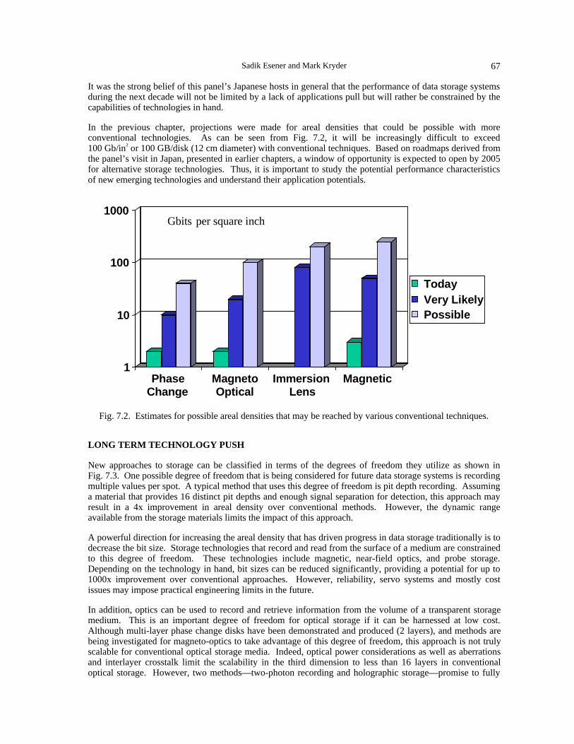
Sadik Esener and Mark Kryder 67
It was the strong belief of this panel’s Japanese hosts in general that the performance of data storage systemsduring the next decade will not be limited by a lack of applications pull but will rather be constrained by thecapabilities of technologies in hand.
In the previous chapter, projections were made for areal densities that could be possible with moreconventional technologies. As can be seen from Fig. 7.2, it will be increasingly difficult to exceed100 Gb/in2 or 100 GB/disk (12 cm diameter) with conventional techniques. Based on roadmaps derived fromthe panel’s visit in Japan, presented in earlier chapters, a window of opportunity is expected to open by 2005for alternative storage technologies. Thus, it is important to study the potential performance characteristicsof new emerging technologies and understand their application potentials.
1
10
100
1000
PhaseChange
MagnetoOptical
ImmersionLens
Magnetic
TodayVery LikelyPossible
Gbits per square inch
Fig. 7.2. Estimates for possible areal densities that may be reached by various conventional techniques.
LONG TERM TECHNOLOGY PUSH
New approaches to storage can be classified in terms of the degrees of freedom they utilize as shown inFig. 7.3. One possible degree of freedom that is being considered for future data storage systems is recordingmultiple values per spot. A typical method that uses this degree of freedom is pit depth recording. Assuminga material that provides 16 distinct pit depths and enough signal separation for detection, this approach mayresult in a 4x improvement in areal density over conventional methods. However, the dynamic rangeavailable from the storage materials limits the impact of this approach.
A powerful direction for increasing the areal density that has driven progress in data storage traditionally is todecrease the bit size. Storage technologies that record and read from the surface of a medium are constrainedto this degree of freedom. These technologies include magnetic, near-field optics, and probe storage.Depending on the technology in hand, bit sizes can be reduced significantly, providing a potential for up to1000x improvement over conventional approaches. However, reliability, servo systems and mostly costissues may impose practical engineering limits in the future.
In addition, optics can be used to record and retrieve information from the volume of a transparent storagemedium. This is an important degree of freedom for optical storage if it can be harnessed at low cost.Although multi-layer phase change disks have been demonstrated and produced (2 layers), and methods arebeing investigated for magneto-optics to take advantage of this degree of freedom, this approach is not trulyscalable for conventional optical storage media. Indeed, optical power considerations as well as aberrationsand interlayer crosstalk limit the scalability in the third dimension to less than 16 layers in conventionaloptical storage. However, two methods—two-photon recording and holographic storage—promise to fully

7. Alternative Storage Technologies68
exploit this degree of freedom by providing potential areal densities in the order of Tb/in2 and possibly at lowcosts. Currently, suitable materials and peripheral optoelectronic devices are still in development.
smaller bits: e.g.,- structured mediumNFO, probe, etc .
multiple layers: e.g. - DVD, 2-photon
multiple valuesper mark: e.g.,Pit depth recording
~4X
500X
1000X
Holographic50-500X
Fig. 7.3. New degrees of freedom in data storage.
Finally, the advances made in optoelectronic device arrays and MEMS may enable data to be accessed inparallel. This may lead to a significant increase in data transfer rates enabling applications such as contentaddressed data mining to become practical.
Advanced Magnetic Storage
As noted earlier in the introduction, longitudinal magnetic recording, which has been increased in arealdensity by approximately 2.5 million times since 1957, is predicted to exhibit superparamagnetic thermalinstabilities in the recordings when the density reaches 36 Gb/in2, which is less than one order of magnitudehigher than the areal density on current disk drives. Some of the Japanese researchers the WTEC teamvisited predicted that conventional longitudinal magnetic recording may be limited to even lower densities,such as 20 Gb/in2, because of grain size variations in the media. Although a change in the bit aspect ratiofrom about 20:1 to the order of 4:1 or 6:1 has been predicted to make it possible to achieve densities of theorder of 100 Gbit/in2, it is inevitable that the technology must change if the rapid 60% per year increase inareal density, which has been the trend for the past seven years, is to continue to much higher densities.
Various new magnetic storage technologies are being explored to circumvent the barriers that thesesuperparamagnetic effects impose. Alternative magnetic storage technologies that the WTEC team sawbeing investigated in Japan included perpendicular magnetic recording, thermally or optically assistedmagnetic recording and patterned media recording. These technologies, the advantages they may offer andthe work being done on them, are discussed in the following sections.
Perpendicular Magnetic Recording
One possible means of extending magnetic recording density beyond what can be achieved usinglongitudinal magnetic recording is to use perpendicular magnetic recording. The medium is magnetizedperpendicular to the film plane, rather than in the plane.
As a result of the perpendicular orientation of the magnetization in the medium, a recorded transition doesnot contain large magnetostatic charge as it does in a longitudinal medium. Instead, magnetostatic charge ismostly at the bottom and top surfaces of the medium. Consequently, whereas in longitudinal magneticrecording the demagnetizing fields tend to increase with recording density and reduce the thermal stability ofthe recordings, in perpendicular magnetic recording the demagnetizing fields tend to decrease with therecording density, possibly enabling higher densities to be recorded, if the code used for recording preventslong strings of zeros (no transitions) from being recorded in the medium.
Moreover, many Japanese researchers argue that thicker media may be used in perpendicular magneticrecording. Since grains typically extend through the medium thickness, by using a thicker medium, the grainvolume, and therefore the stability of the medium against superparamagnetism, is enhanced.
Sadik Esener and Mark Kryder 69
Finally, with perpendicular magnetic recording, it is, in principle, possible to fabricate the medium on a highpermeability magnetic underlayer. This causes an image of the main pole of the recording head to be formedin the underlayer, so that the medium is effectively in the gap of the head. Whereas with conventionallongitudinal magnetic recording, the recording is done with the fringing field from the head, withperpendicular recording using a high permeability magnetic underlayer, the perpendicular medium iseffectively placed in the gap of the head. This enables much higher write fields from the recording head,which in turn enable much higher anisotropy (and therefore more thermally stable) magnetic materials to berecorded.
Exactly how large the advantage of perpendicular recording is with regard to extending the recording densitybeyond what can be achieved with longitudinal recording is not yet clear; however, most researchers doadmit that it probably does offer some advantage. Although U.S. companies worked on perpendicularmagnetic recording in the early 1980s, there has not been much activity since; whereas in Japan there hasbeen a continuous effort since the late 1970s, and it is clear that the Japanese are considerably moreknowledgeable about the technology than U.S. researchers in the field. Thus, the U.S. magnetic disk driveindustry is at some risk with regard to finding itself behind its Japanese competitors if a switch toperpendicular magnetic recording comes when the superparamagnetic limits of longitudinal recording havebeen reached.
Thermally Assisted Magnetic Recording
As noted in the introduction, superparamagnetic thermal instability occurs in a medium when the magneticanisotropy energy KUV of a grain of the medium becomes sufficiently small that thermal energy KBT maycause the magnetization to switch. Hence, to increase the thermal stability of the medium, it is necessary toincrease the magnetic anisotropy energy density KU. However, if the magnetic anisotropy becomes too large,it may become impossible to produce the field necessary to record on the medium with available magneticrecording head materials.
One way to overcome this barrier is to use thermally assisted magnetic recording.
Heating a magnetic material generally causes the magnetic anisotropy energy density KU to decrease. Hence,the idea of thermally assisted magnetic recording is to use thermal energy to lower the KU of a mediumsufficiently that it may be written with available magnetic recording head materials and then to cool themedium back to ambient conditions, so that the thermal stability of the large KU material is achieved.
Continuously exchange coupled perpendicularly oriented magnetic media like that used for magneto-opticrecording may be written in this manner, and recent work has shown that domains as small as 20 nm arestable for times in excess of 10 years in such media.
Thermally assisted magnetic recording is commonly used in magneto-optic recording, where a focused laserbeam is used to heat the medium; however, magneto-optic recording uses the Kerr (or Faraday) magneto-optic effects for readout of the recorded information. Since the magneto-optic effects are relatively small, itis difficult to achieve high signal-to-noise ratio when reading out by this technique, and the bandwidth ofmagneto-optic disk drives is typically restricted to smaller values than magnetic disk drives.
It was suggested by Dr. Miura of Fujitsu Laboratories (during his presentation to WTEC of the researchbeing carried out by the Storage Research Consortium and ASET) that an approach using optically assistedwriting and magnetic readout may have merit to overcome both of these limitations.
Patterned Media Magnetic Recording
Yet another method of overcoming the barrier to increasing the areal density of magnetic recording imposedby superparamagnetic effects is to use patterned or structured media.
In conventional magnetic recording, to achieve an acceptable signal-to-noise ratio, it necessary that there beof the order of 100 grains in the volume of a bit cell. This is because the transitions tend to follow the grainboundaries, and therefore have a significant variance in their position relative to where they were intended tobe written. By making the grain size smaller with respect to the bit cell dimensions, the variance is reduced.
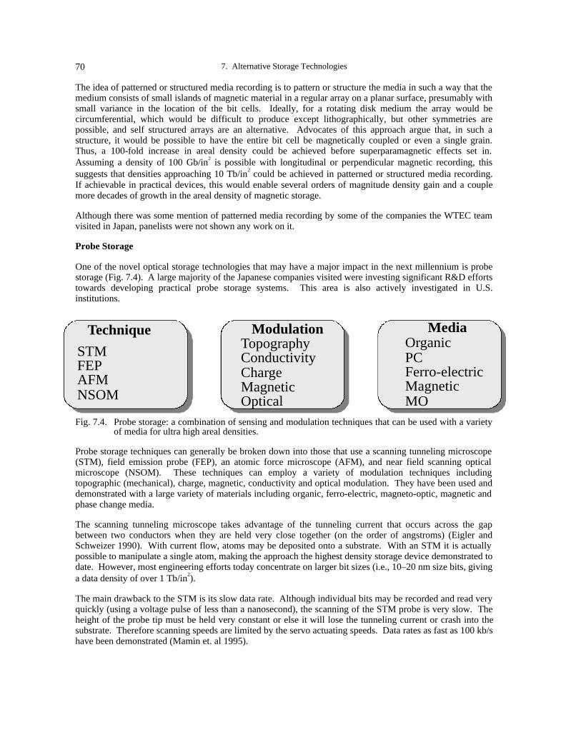
7. Alternative Storage Technologies70
The idea of patterned or structured media recording is to pattern or structure the media in such a way that themedium consists of small islands of magnetic material in a regular array on a planar surface, presumably withsmall variance in the location of the bit cells. Ideally, for a rotating disk medium the array would becircumferential, which would be difficult to produce except lithographically, but other symmetries arepossible, and self structured arrays are an alternative. Advocates of this approach argue that, in such astructure, it would be possible to have the entire bit cell be magnetically coupled or even a single grain.Thus, a 100-fold increase in areal density could be achieved before superparamagnetic effects set in.Assuming a density of 100 Gb/in2 is possible with longitudinal or perpendicular magnetic recording, thissuggests that densities approaching 10 Tb/in2 could be achieved in patterned or structured media recording.If achievable in practical devices, this would enable several orders of magnitude density gain and a couplemore decades of growth in the areal density of magnetic storage.
Although there was some mention of patterned media recording by some of the companies the WTEC teamvisited in Japan, panelists were not shown any work on it.
Probe Storage
One of the novel optical storage technologies that may have a major impact in the next millennium is probestorage (Fig. 7.4). A large majority of the Japanese companies visited were investing significant R&D effortstowards developing practical probe storage systems. This area is also actively investigated in U.S.institutions.
Technique
STMFEP AFMNSOM
ModulationTopographyConductivity ChargeMagneticOptical
MediaOrganicPC Ferro-electricMagneticMO
Fig. 7.4. Probe storage: a combination of sensing and modulation techniques that can be used with a varietyof media for ultra high areal densities.
Probe storage techniques can generally be broken down into those that use a scanning tunneling microscope(STM), field emission probe (FEP), an atomic force microscope (AFM), and near field scanning opticalmicroscope (NSOM). These techniques can employ a variety of modulation techniques includingtopographic (mechanical), charge, magnetic, conductivity and optical modulation. They have been used anddemonstrated with a large variety of materials including organic, ferro-electric, magneto-optic, magnetic andphase change media.
The scanning tunneling microscope takes advantage of the tunneling current that occurs across the gapbetween two conductors when they are held very close together (on the order of angstroms) (Eigler andSchweizer 1990). With current flow, atoms may be deposited onto a substrate. With an STM it is actuallypossible to manipulate a single atom, making the approach the highest density storage device demonstrated todate. However, most engineering efforts today concentrate on larger bit sizes (i.e., 10–20 nm size bits, givinga data density of over 1 Tb/in2).
The main drawback to the STM is its slow data rate. Although individual bits may be recorded and read veryquickly (using a voltage pulse of less than a nanosecond), the scanning of the STM probe is very slow. Theheight of the probe tip must be held very constant or else it will lose the tunneling current or crash into thesubstrate. Therefore scanning speeds are limited by the servo actuating speeds. Data rates as fast as 100 kb/shave been demonstrated (Mamin et. al 1995).
Sadik Esener and Mark Kryder 71
Materials have been developed for read/write/erase applications using STM which undergo phase change(which changes their electrical conductivity); however, these materials may suffer from fatigue and slowrecording times (Sato and Tsukamoto 1993).
The atomic force microscope employs a cantilevered tip that is scanned across a sample. In this case the tipis usually in contact with the sample surface. Features on the surface of the sample cause deflections of thetip that can be detected optically by monitoring the back surface of the tip with a laser and split photodiodedetector.
Write once read only memory (WORM) writing with an AFM may be achieved using a thermo-mechanicalprocess. The position of the AFM tip is placed concurrent with the focal point of a laser. When a pulse issent out from the laser it locally heats the area around the tip causing the tip to sink into the polymer substratecreating a pit. Using this technique, pits as small as 100 nm have been recorded giving a recording density ofroughly 30 Gb/in2. The recording speed for that experiment was 200 kb/s and readout was up to 1.25 Mb/s.
It may also be possible to produce inexpensive ROM replicas readable by an AFM. Disc “masters” havebeen fabricated using e-beam lithography (Terris et al. 1996). The masters have then been used to replicatedata in a photo-polymer. Features as small as 50 nm have been successfully replicated.
Read/write/erase AFM storage has been done in a number of different materials including charge trappingmaterials such as nitride-oxide-semiconductor (NOS) layers (Fujiwara, Kojima and Seto 1996) and alsophase change materials the same those being used in optical discs (Kado and Tohda 1995). The smallest bitsthat have been recorded are on the order of 75 nm giving a recording density of over 100 Gb/in2. Readoutrates of 30 kb/s have been achieved, but predicted rates of up to 10 Mb/s may be possible.
The major obstacle for AFM storage is tip wear. The tip is slowly worn down as it drags across the sample,reducing the resolution of the readout.
Near-field optical recording includes any technology that allows one to surpass the areal density limitimposed by the diffraction of light in optical data storage. Near field scanning optical microscopy (NSOM)combats the effects of diffraction on the optical spot size by placing the pick up heads very near (about50 nm above) the media. A near-field probe can produce spots as small as 40 nm in diameter andconceptually can achieve areal densities in the order of 100 Gb/in2. The problem is that the probe must benear contact with the medium, making it difficult to prevent head crashes and support removable media.
One of the original near-field recording techniques was through the use of a tapered fiber (Betzig et al. 1992).The tip of a fiber, which is smaller than the wavelength of the recording light, is positioned within 10 nm ofthe sample. Using magneto-optic materials, bits as small as 60 nm have been recorded and read out. Thetapered fiber approach suffers from very low optical efficiency.
STM, AFM and NSOM can all provide ultra high areal densities. However, the total area available forstorage restricts the capacity per device (chip). Assuming a scan area of 1cm2, 30 nm effective spot sizeyields a total capacity of 10 GB only. Yet using parallel access and MEMS technology, relatively fast accesscan be achieved. Considering the low power nature of these approaches, we expect this type of probe storageto have a potential market for applications that require portability.
Perhaps a more scalable approach, in terms of capacity per device, is the use of a solid immersion lens (SIL)(Terris et. al 1994; Terris, Mamin and Rugar 1996; Ichimura, Hayashi and Kino 1997). The SIL reduces theactual spot size by both refracting the rays at the sphere surface and by having an increased index ofrefraction (up to n = 2) within the lens. However, this small spot size can only exist within the SIL;therefore, the evanescent wave from the bottom surface of the lens must be used for recording. This meansthat the SIL must be held within 100 nm or less of the recording surface. Maintaining such a distance over arapidly spinning disc is possible using a technique borrowed from hard disk storage: the flying head. Theflying head floats on a cushion of air above the disc and is able to hold the head in very close proximity to thedisc without crashing. SILs have been fabricated with equivalent numerical aperture of up to 1.8. Using780 nm wavelength, recording spot sizes on the order of 320 nm have been achieved, giving recording

7. Alternative Storage Technologies72
densities on the order of 3 Gb/in2. Using the flying head, data rates of up to 3 Mb/s were achieved, and datarates of up to 15 Mb/s may be possible.
During the WTEC panel’s visit to Japan, panelists saw significant progress in various areas of probe storage.This includes hybrid STM/AFM systems, automated Langmuir-Blodgett film deposition systems, neworganic polymers (Fig. 7.5), record breaking small recorded spots (Fig. 7.6 and Fig. 7.7), and probefabrication techniques (Fig. 7.8) that can lead to low cost manufacturable systems. Dr. Ohta at Matsushitaperhaps best underlined the expectations of Japanese researchers in probe storage by stating that, “phasechange media welcomes probe storage.”
Fig. 7.5. Recording by STM/AFM probe in organic LB films (Yano et al. 1996).
2.4x1.9µm2
Fig. 7.6. Probe storage at Canon: (a) record breaking spot sizes were achieved using organic LBfilms over an area as large as 4 micron square (Yano et al. 1996).
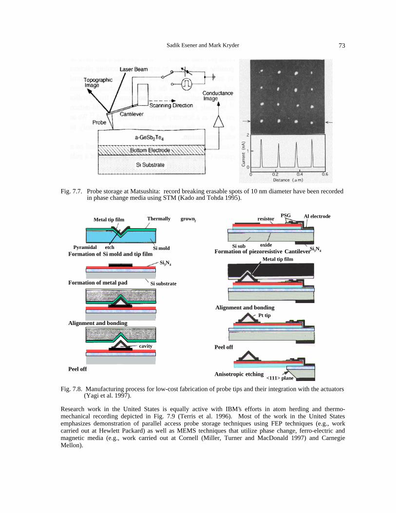
Sadik Esener and Mark Kryder 73
Fig. 7.7. Probe storage at Matsushita: record breaking erasable spots of 10 nm diameter have been recordedin phase change media using STM (Kado and Tohda 1995).
Metal tip film Thermally grown2
Pyramidal etchFormation of Si mold and tip film
Formation of metal pad
Alignment and bonding
Peel off
cavity
Si3N4
Si substrate
Si mold
resistorPSG Al electrode
Si3N4
oxideSi subFormation of piezoresistive Cantilever
Metal tip film
Alignment and bonding
Peel off
Anisotropic etching<111> plane
Pt tip
Fig. 7.8. Manufacturing process for low-cost fabrication of probe tips and their integration with the actuators(Yagi et al. 1997).
Research work in the United States is equally active with IBM’s efforts in atom herding and thermo-mechanical recording depicted in Fig. 7.9 (Terris et al. 1996). Most of the work in the United Statesemphasizes demonstration of parallel access probe storage techniques using FEP techniques (e.g., workcarried out at Hewlett Packard) as well as MEMS techniques that utilize phase change, ferro-electric andmagnetic media (e.g., work carried out at Cornell (Miller, Turner and MacDonald 1997) and CarnegieMellon).

7. Alternative Storage Technologies74
Near field optical storage using the SIL techniques is being investigated both in Japan and in the UnitedStates. Terastor, a start-up company in the United States, is working towards commercialization of amagneto-optic disk system that utilizes an SIL lens. Several Japanese drive manufacturers are involved withTerastor’s activities and are pursuing separate R&D efforts as well. Institutions involved in this directioninclude NAIR, Hitachi, Fujitsu, and Toshiba.
Fig. 7.9. Thermo-mechanical recording at IBM using rotating plastic disk using an atomic force microscopetip. At selected locations, electrical current was pulsed through the tip causing the tip to be heated.The heat from the tip softens the substrate and the pressure from the tip causes an indentation to beformed. Marks smaller than 0.1 micron can be written in this manner (Mamin et al. 1995).
100 102 104 106 108 1010
1015
1014
1013
1012
1011
1010
109
108
Atom HerdingSTM
STM/AFM PC(NEC, Matsushita)
STM FieldEvaporation
NSOM(ATT)
NOS Charge store(Stanford)
AFMThermomechanical
CD-ROM
Magneto-Optical
MagneticSIL
NOS Charge store(I BM)
Den
sity
(bi
ts/in
2 )
Data Rate (bits/s)
STM/AFM LB(Canon)
Fig. 7.10. Classification and demonstrated performance of probe storage and comparison with presentstorage techniques. Recent results from Canon and Matsushita have been added to the figure(Modified after IBM) (Mamin et al. 1995).
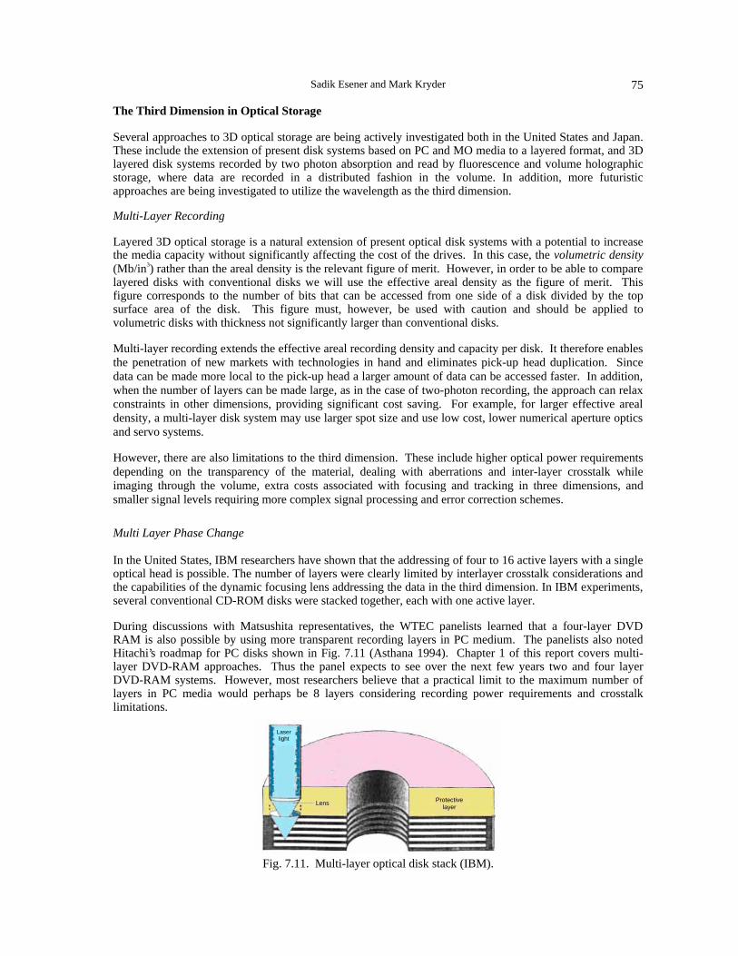
Sadik Esener and Mark Kryder 75
The Third Dimension in Optical Storage
Several approaches to 3D optical storage are being actively investigated both in the United States and Japan.These include the extension of present disk systems based on PC and MO media to a layered format, and 3Dlayered disk systems recorded by two photon absorption and read by fluorescence and volume holographicstorage, where data are recorded in a distributed fashion in the volume. In addition, more futuristicapproaches are being investigated to utilize the wavelength as the third dimension.
Multi-Layer Recording
Layered 3D optical storage is a natural extension of present optical disk systems with a potential to increasethe media capacity without significantly affecting the cost of the drives. In this case, the volumetric density(Mb/in3) rather than the areal density is the relevant figure of merit. However, in order to be able to comparelayered disks with conventional disks we will use the effective areal density as the figure of merit. Thisfigure corresponds to the number of bits that can be accessed from one side of a disk divided by the topsurface area of the disk. This figure must, however, be used with caution and should be applied tovolumetric disks with thickness not significantly larger than conventional disks.
Multi-layer recording extends the effective areal recording density and capacity per disk. It therefore enablesthe penetration of new markets with technologies in hand and eliminates pick-up head duplication. Sincedata can be made more local to the pick-up head a larger amount of data can be accessed faster. In addition,when the number of layers can be made large, as in the case of two-photon recording, the approach can relaxconstraints in other dimensions, providing significant cost saving. For example, for larger effective arealdensity, a multi-layer disk system may use larger spot size and use low cost, lower numerical aperture opticsand servo systems.
However, there are also limitations to the third dimension. These include higher optical power requirementsdepending on the transparency of the material, dealing with aberrations and inter-layer crosstalk whileimaging through the volume, extra costs associated with focusing and tracking in three dimensions, andsmaller signal levels requiring more complex signal processing and error correction schemes.
Multi Layer Phase Change
In the United States, IBM researchers have shown that the addressing of four to 16 active layers with a singleoptical head is possible. The number of layers were clearly limited by interlayer crosstalk considerations andthe capabilities of the dynamic focusing lens addressing the data in the third dimension. In IBM experiments,several conventional CD-ROM disks were stacked together, each with one active layer.
During discussions with Matsushita representatives, the WTEC panelists learned that a four-layer DVDRAM is also possible by using more transparent recording layers in PC medium. The panelists also notedHitachi’s roadmap for PC disks shown in Fig. 7.11 (Asthana 1994). Chapter 1 of this report covers multi-layer DVD-RAM approaches. Thus the panel expects to see over the next few years two and four layerDVD-RAM systems. However, most researchers believe that a practical limit to the maximum number oflayers in PC media would perhaps be 8 layers considering recording power requirements and crosstalklimitations.
Laserlight
Lens Protectivelayer
Fig. 7.11. Multi-layer optical disk stack (IBM).

7. Alternative Storage Technologies76
Multi-Layer MO
The success of double layer DVD-ROM has attracted interest in whether it is possible to use multiple layerswith the MO media. A possible approach is shown in Fig. 7.12 (Nakagawa et al. 1997). The disk mediumconsists of two active TbFeCo MO layers, one modified by the presence of an additional PtCo layer. Thusthe characteristics of the two recording layers are slightly different in terms of required power andwavelength. This difference is exploited by wavelength selective thermo-magnetic recording to selectivelyrecord onto each layer using two different lasers of different wavelengths. During readout the effect of thetwo layers on the polarization state of the readout beam is additive on the polarization state of a read-outbeam. However, since the total Kerr rotation angle of two reflected waves of two different wavelengths isdependent on the linear combination of the retardation imposed by each layer, by detecting each waveindependently it is possible to calculate the state of the recorded bits in each layer. This requires the solutionof a linear system of two equations with two unknowns (the bit states) in real time, a rather straightforwardoperation with present capabilities of electronics.
It is possible in theory to extend this approach to more than two layers using more than two wavelengths.However, the number of lasers, optical components and receiver circuits as well as the head mass grow withgrowing number of layers. Nevertheless, this approach can significantly benefit from technologies beingdeveloped for wavelength division multiplexing (WDM) communication over fiber optic networks and mayfuel their manufacturability further. This type of forward-looking R&D in Japan demonstrates theimportance attributed to multi-layer recording approaches.
Substrate
SiN
TbFeCoSiN
TbFeCoPtCo
Dichroic mirror
Laser 1
Laser2
Detector2
Detector1
PBS1
PBS2 X1
X2
Layer 1
Layer 2
Fig. 7.12. University of Tokyo and Hitachi Maxell Ltd.’s approach to double layer MOdisk recording and readout.
Two-Photon Recording: Extending Multi-Layer Recording to More than a Hundred Layers
The two-photon recording approach used by Call/Recall, Inc. in the United States relies on recording bits in avolume by using two-photon absorption (Hunter et al. 1990). As described in Fig. 7.13, a spot is written inthe volume of a molded organic polymer only in locations where two beams with sufficient photon energies,one carrying the information and the other specifying the location, intersect temporally and spatially. Therecorded bits are then read by fluorescence when excited by single photons absorbed within the written spotvolume.

Sadik Esener and Mark Kryder 77
S0
S1
S2
S0
S1
532 nm
1064 nm
532 nm’read’
fl.’write’abs.
X10 s-9
10 s-11
Fig. 7.13. Principle of two-photon recording in 3D (Call/Recall, Inc.).
Using this method, multiple layer ROM disk recording, and readout with a portable unit, have beendemonstrated as shown in Fig. 7.14. The results indicate no crosstalk between layers spaced as close as30 µm and excellent stability of the written bits at room temperature. The spot size is limited by therecording wavelengths through diffraction as well as by the sensitivity and integration time of the read-outdetector used. The approach promises low cost, ultra high effective areal density (1-100 Tb/in2) removabledisk media with thousands of layers for image and video applications. In addition to the extremely largevolumetric densities achievable with this monolithic 3D disk approach, the stored data can be accessed inparallel leading to high data transfer rates suitable for content-based search operations.
diskCCD
laser
Portable 3D disk player
Fig. 7.14. Multi-layer 3D ROM disk reader on the left; side view of a disk showing many recorded layers; andthe oscilloscope trace related to detected bit stream with the disk rotating at 5,000 rpm (Call/Recall,Inc.).
However, several issues remain to be resolved. So far only small (1.5 inch diameter) disks have beendemonstrated. Although insensitive to media shrinkage, the approach is affected by surface quality andvolumetric homogeneity of the media. The cost of short pulse-high intensity lasers required for two-photonrecording is still too high to consider their use in a consumer product. Finally, materials capable of writingand erasing without fatigue are yet to be demonstrated for addressing a larger span of applications.
The potential impact of layered 3D optical disks on the capacity per disk can be much greater than the impactof, for example, blue lasers. This is because the capacity is directly proportional to the number of layers.Assuming relaxed areal densities, 3D disks provide the potential for realizing disks with 100 GB to 1 TBcapacities before 2005 as shown in Fig. 7.15. In addition to Call/Recall, Inc., two-photon recording is alsobeing investigated at the Jet Propulsion Laboratory in the United States and at Osaka University in Japan(Toriumi, Hermann and Kawata 1997). At this point in time, two-photon recording appears to be a potentialcontender for future removable ultra-high capacity optical disk storage.

7. Alternative Storage Technologies78
Holographic Storage
In bit-oriented memories if any portion of the storage media is damaged or blocked, the data stored in thatregion is lost. This is not the case for holographic storage, where the information about each stored bit isdistributed throughout a large region. If a portion of the holographic storage media is damaged or blocked,instead of causing catastrophic loss of some of the data, all of the data are partially degraded. For commontypes of damage, such as surface dust or smudges, holograms are remarkably robust. This has generatedinterest in holographic data storage, and despite the more complex optical systems, high cost media, andsources with good spatial coherence required, there has been continued research in the field since the early1960s (Solymar and Cooke 1981).
Holograms are created by recording the interference pattern of two optical wavefronts. The storage mediacan record the fringes as index and/or amplitude modulation. When the recording is illuminated by one ofthe wavefronts (the reference beam), the other wavefront (the object beam) is reproduced.
2010Year
2000 2005
1T
10G
1G
100M
100G
Effe
ctiv
e R
ecor
ding
Den
sity
(bi
ts/in
2 )
250L
500L
2-photonareal density/layer
ASMOplan
magneticrecording
10T
TeraStorplan
2-Photon Multi-layer
DVDplan
Fig. 7.15. Potential impact of 3D multi-layer optical storage and its comparison with conventional datastorage and new emerging techniques such as SIL (compiled from data obtained from TerastorWeb site, OITDA storage roadmap and Call/Recall, Inc. internal reports).
Since the diffraction efficiency of amplitude holograms is limited to 6–7%, and the efficiency of volumeamplitude holograms is limited to 33%, volume phase holograms with their diffraction efficiencyapproaching 100% are best suited for storage applications. In addition, the Bragg selectivity of volumeholograms allows the volume multiplexing (by angle or wavelength or combination) of many pages of datawith small crosstalk between the pages.
Photorefractive crystals (PRC) and photo-polymers are typically used in demonstration experiments both fornon-moving and volumetric disk type applications. These materials are recorded at room temperature, andthe inorganic PRCs offer high photocyclicity. Using PRCs, 10,000 images were successfully stored andretrieved (Mok and Stoll 1992). More recently, hero experiments have demonstrated effective areal densitiesin excess of 64 Gb/in2.
The main drawback of the approach with PRCs is the high cost of materials, the decrease in diffractionefficiency with increasing number of multiplexed holograms and read-out cycles, and the relatively small andslow changes in the index of refraction. To circumvent these problems, significant progress has been madein terms of using recording schedules to improve the uniformity of the recorded data, fixing procedures topermanently store data in PRCs, and new recording geometries to minimize crosstalk. In addition, more
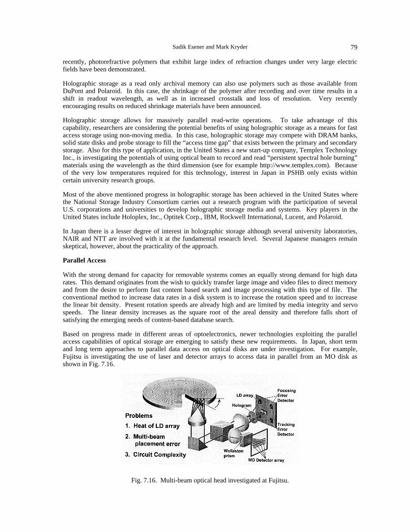
Sadik Esener and Mark Kryder 79
recently, photorefractive polymers that exhibit large index of refraction changes under very large electricfields have been demonstrated.
Holographic storage as a read only archival memory can also use polymers such as those available fromDuPont and Polaroid. In this case, the shrinkage of the polymer after recording and over time results in ashift in readout wavelength, as well as in increased crosstalk and loss of resolution. Very recentlyencouraging results on reduced shrinkage materials have been announced.
Holographic storage allows for massively parallel read-write operations. To take advantage of thiscapability, researchers are considering the potential benefits of using holographic storage as a means for fastaccess storage using non-moving media. In this case, holographic storage may compete with DRAM banks,solid state disks and probe storage to fill the “access time gap” that exists between the primary and secondarystorage. Also for this type of application, in the United States a new start-up company, Templex TechnologyInc., is investigating the potentials of using optical beam to record and read “persistent spectral hole burning”materials using the wavelength as the third dimension (see for example http://www.templex.com). Becauseof the very low temperatures required for this technology, interest in Japan in PSHB only exists withincertain university research groups.
Most of the above mentioned progress in holographic storage has been achieved in the United States wherethe National Storage Industry Consortium carries out a research program with the participation of severalU.S. corporations and universities to develop holographic storage media and systems. Key players in theUnited States include Holoplex, Inc., Optitek Corp., IBM, Rockwell International, Lucent, and Polaroid.
In Japan there is a lesser degree of interest in holographic storage although several university laboratories,NAIR and NTT are involved with it at the fundamental research level. Several Japanese managers remainskeptical, however, about the practicality of the approach.
Parallel Access
With the strong demand for capacity for removable systems comes an equally strong demand for high datarates. This demand originates from the wish to quickly transfer large image and video files to direct memoryand from the desire to perform fast content based search and image processing with this type of file. Theconventional method to increase data rates in a disk system is to increase the rotation speed and to increasethe linear bit density. Present rotation speeds are already high and are limited by media integrity and servospeeds. The linear density increases as the square root of the areal density and therefore falls short ofsatisfying the emerging needs of content-based database search.
Based on progress made in different areas of optoelectronics, newer technologies exploiting the parallelaccess capabilities of optical storage are emerging to satisfy these new requirements. In Japan, short termand long term approaches to parallel data access on optical disks are under investigation. For example,Fujitsu is investigating the use of laser and detector arrays to access data in parallel from an MO disk asshown in Fig. 7.16.
Fig. 7.16. Multi-beam optical head investigated at Fujitsu.

7. Alternative Storage Technologies80
Issues including heat extraction from laser diode arrays, multi-beam positioning errors, packaging and signalprocessing circuit complexity for post processing are being investigated.
A more futuristic approach being explored at the University of Tokai by Prof. Goto and his group is shown inFig. 7.17. This approach involves the use of VCSEL arrays flying directly above an optical disk mediumusing a near field geometry. The laser is used to both record and directly detect the presence of a bit basedon the optical signal that is fed back into the laser. In order to achieve high data rates, massively parallelaccess through VCSEL array is contemplated as described in Fig. 7.18.
Fig. 7.17. Use of a VCSEL for recording and readout in a near field optics geometry.
In the United States, Quinta, Inc., recently acquired by Seagate, Inc., a manufacturer of magnetic hard drives,has been developing a method to access several optical disk surfaces in parallel using optical fibers. Thefibers are used for distributing the laser power to the head and back to the receivers for readout, and a noveloptoelectronic switch is used to selectively access data on various plates. Also in the United States,Call/Recall, Inc., jointly with Hewlett Packard Company and Optical Micro Machines, is investigating theuse of VCSEL arrays and MEMS to facilitate parallel access to multi-layer disks. In addition, R&D onmassively parallel accessing of holographic data storage systems is also underway as described earlier.
It is believed that parallel access is a viable method to increase the data transfer rate of optical and probestorage systems. The issue is rather when the necessary components that can enable massively parallel datatransfer may provide a favorable cost entry point to market such systems.
Fig. 7.18. Schematic of a VCSEL array access with a massively parallel near field optics architecture tooptical disks promising TB capacities and Tb/s data transfer.

Sadik Esener and Mark Kryder 81
Mastering and Replication Technologies
One of the key areas in optical data storage for ROM type applications is the high fidelity replication process.In this area of R&D significant investments are being made by Japan’s key CD-ROM and DVD-ROMmanufacturers. The mastering effort ranges development of SIL lenses and large area electron beamlithography to the development of ultra short wavelength lasers and probe mastering techniques. Supportingtechnologies including high precision injection molding and ultra smooth polishing techniques are beingdeveloped as well. A potential roadmap derived from OITDA’s roadmap for mastering and replication isshown in Fig. 7.19. At this point in time, we do not know of a development effort of this magnitude in thisarea in the United States.
100G
10G
1G1995 2000 2005
UVMastering
2010 2015
1T
10T
E-beam mastering
260nmSIL
Mastering
Ultra Large Aperture lenses
High density cutting photoresist
Nano-imprinting
ProbeMastering
H-precision injection molding
Ultra smooth substrate
Fig. 7.19. Roadmap for mastering and replication (compiled based on data available fromOITDA, discussions during Sony site visit and various private discussions).
TECHNOLOGY COMPARISON
From the above discussion, it is clear that significant R&D activity is in place both in the United States andJapan to develop alternative storage techniques to address windows of opportunity that may presentthemselves in the second part of the next decade as shown in Fig. 7.20.
At this point it appears that magnetic perpendicular recording and structured media are well placed to takehard disk drives well into the next decade, satisfying general purpose computing requirements. It is possiblethat with these technologies 200 GB capacity hard disk drives will be available within the next decade.
In terms of replacing conventional removable optical disk storage for video-type applications, the UnitedStates seems to put more emphasis in its R&D effort into SIL lens approaches with Terastor and into truevolumetric storage development with holographic storage and two-photon recording technologies. MostJapanese effort in this area seems to be focused on improving conventional optical disk technologies wherethe Japanese have a strong lead. Both countries are investigating the merits of thermo-mechanical recordingon moving polymer disks, perhaps for mastering purposes.
Both countries seem to be pursuing parallel accessing techniques for optical storage, relying on progressmade in optoelectronic array devices as well as MEMS actuators.
Surfa
ce
Re
co
rdin
g D
ens
ity (
bits
/in2 )
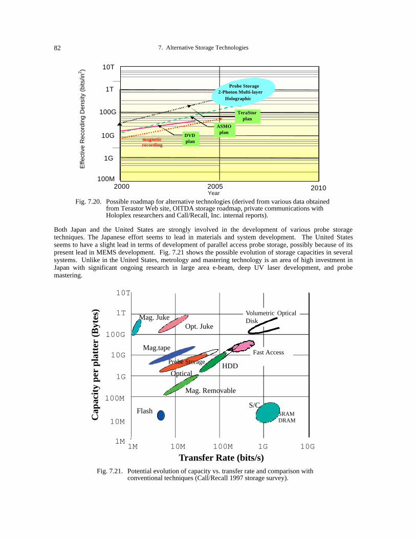
7. Alternative Storage Technologies82
2010Year
2000 2005
1T
10G
1G
100M
100G
magneticrecording
10T
TeraStorplan
DVDplan
2-Photon Multi-layer
ASMOplan
Probe Storage
Holographic
Effe
ctiv
e R
ecor
ding
Den
sity
(bi
ts/in
2 )
Fig. 7.20. Possible roadmap for alternative technologies (derived from various data obtainedfrom Terastor Web site, OITDA storage roadmap, private communications withHoloplex researchers and Call/Recall, Inc. internal reports).
Both Japan and the United States are strongly involved in the development of various probe storagetechniques. The Japanese effort seems to lead in materials and system development. The United Statesseems to have a slight lead in terms of development of parallel access probe storage, possibly because of itspresent lead in MEMS development. Fig. 7.21 shows the possible evolution of storage capacities in severalsystems. Unlike in the United States, metrology and mastering technology is an area of high investment inJapan with significant ongoing research in large area e-beam, deep UV laser development, and probemastering.
Cap
acit
y pe
r pl
atte
r (B
ytes
)
Transfer Rate (bits/s)
Flash
Mag. Removable
HDDOptical
Opt. JukeMag. Juke
Mag.tape
1T
100G
10G
1G
100M
10M
1M1M 10M 100M 1G 10G
10T
DRAM
Volumetric OpticalDisk
Fast Access
Probe Storage
S/CSRAM
Fig. 7.21. Potential evolution of capacity vs. transfer rate and comparison withconventional techniques (Call/Recall 1997 storage survey).

Sadik Esener and Mark Kryder 83
CONCLUSION
As described in Table 7.1, several emerging technologies are well placed to capture new markets fromconventional storage technologies by the second half of the next decade.
Table 7.1Emerging Technologies and Applications
Technology Applications Performance
Structured magnetic media
SIL lens near-field MO disks
General purpose, computing 200 GB, ms access
Volumetric disks Advanced video, removable 200 GB-1 TB, 1 Gb/s data rate
Thermo-mechanical probe (disks) Mastering 1 TB and more, Mb/s data rate
Probe storage (chips) Portable video applications 10 GB, µs access, 100 Mb/s
U.S. manufacturers of magnetic hard drives and related research institutions must invest in research inperpendicular recording and especially in structured magnetic media and related components where theirJapanese counterparts seem to have a head start. In the area of optical storage, short-term favorite candidatesfor success for the U.S. effort are Quinta or TeraStor, which are exploiting fiber optics and SIL lenses,respectively. However, these techniques strongly depend on several technological areas where Japan has alead.
For the longer term and significant gain in market share, removable volumetric parallel accessible storagesystems such as holographic and/or two-photon approaches appear attractive. The key issue for holographicstorage is the development of an inexpensive, reliable write-once material. Two-photon recording canbenefit from the development of a higher sensitivity write-once material and preferably from an erasablematerial. These technologies are especially important since they can drive the low-cost manufacturing ofoptoelectronic and MEMS device arrays that can be critical for many other applications areas.
Probe storage is clearly an important area for future investment, particularly for very small or very low powerstorage devices. It has the potential of capturing a new market segment, that of portable digital videoequipment.
Japan seems to be clearly ahead in developing metrology, mastering and replication technologies. TheUnited States must invest in these critical areas since they serve many other manufacturing areas as well.
Micro-machining can find a high-volume application in the disk drive industry and probe storage. TheUnited States has a slight lead in research, but a high-volume application and the investment it draws couldquickly evaporate that lead. Japan can easily take the lead in micro-machining away from the United Stateswith its process development strength.
REFERENCES
Asthana, P. 1994. A long road to overnight success. IEEE Spectrum. October: 60-66.
Betzig, E., J.K. Trautman, R. Wolfe, E.M. Gyorgy, P.L. Finn, M.H. Kryder, and C.H. Chang. 1992. Near-field magneto-optics and high density data storage. Appl. Phys. Lett. 61: 142.
Christenson, G.L., S.A. Miller, Z.H. Zhu, N.C. MacDonald, and Y.H. Lo. 1995. Optical reading and writing on GaAsusing an atomic force microscope. Appl. Phys. Lett. 66: 2780.
Eigler, D.M. and E.K. Schweizer. 1990. Nature. 344: 524.
Fujiwara, I., S. Kojima, and J. Seto. 1996. High density charge storage memory with scanning probe microscopy. Jpn.J. Appl. Phys. 35: 2764.
Hunter, S., F. Kiamelev, S. Esener, D.A. Parthenopoulos, and P.M. Rentzepis. 1990. Potentials of 2-photon based 3-Doptical memories for high performance computing. Applied Optics 29: 2058-2066.
7. Alternative Storage Technologies84
Ichimura, I., S. Hayashi, and G. S. Kino. 1997. High-density optical recording using a solid immersion lens. Appl. Opt.36: 4339.
Kado, H. and T. Tohda. 1995. Nanometer-scale recording on chalcogenide films with an atomic force microscope.Appl. Phys. Lett. 66: 2961.
Mamin, H.J., B.D. Terris, L.S. Fan, S. Hoen, R.C. Barret, and D. Rugar. 1995. High-density data storage using proximalprobe-techniques. IBM J. Res. Develp. 39: 681.
Miller, S.A., K.L. Turner, and N.C. MacDonald. 1997. Microelectromechanical scanning probe instruments for arrayarchitectures. Rev. Sci. Instrum. 68: 4155.
Mok. F. and H. M. Stoll. 1992. Holographic inner product processor for pattern recognition. In Proc. SPIE 1701: 312.
Nakagawa, K., A. Itoh, K. Shimazake and N. Ohta. 1997. Multi-valued MO recording and multi-wavelength readout.IEEE Trans. On Magnetics. 33(5). September: 3235.
Sato, A. and Y. Tsukamoto. 1993. Nanometre-scale recording and erasing with the scanning tunnelling microscope.Nature 363: 431.
Solymar L. and D.J. Cooke. 1981. Volume holography and volume gratings. Academic Press.
Terris, B.D., H.J. Mamin, and D. Rugar. 1996. Near-field optical data storage. Appl. Phys. Lett. 68: 141.
Terris, B.D., H.J. Mamin, D. Rugar, W.R. Studenmund, and G.S. Kino. 1994. Near-field optical data storage using asolid immersion lens. Appl. Phys. Lett. 65: 388.
Terris, B.D., H.J. Mamin, M.E. Best, J.A. Logan, D. Rugar, and S.A. Rishton. 1996. Nanoscale replication for scanningprobe data storage. Appl. Phys. Lett. 69: 4262.
Terris, B.D., H.J. Mamin, M.E. Best, J.A. Logan and D. Rugar, S.A. Rishton. 1996. Nanoscale replication for scanningprobe data storage. Appl. Phys. Lett. 69(27). Dec: 4262.
Toriumi, A., J.M. Hermann, S. Kawata. 1997. Nondestructive readout of a three-dimensional photochromic opticalmemory with a near infrared differential phase-contrast microscope. Optics Letters 22(8). April 15: 555.
Yagi, T., Y. Shimata, T. Ikeda, O. Takamatsu, K. Takimoto, and Y. Hiraj,. 1997. A new method to fabricate metal tipsfor scanning probe microscopy. T.IEE Japan: 117-E (8).
Yano, K., et al. 1996. Information storage using conductance change of Langmuir-Blodgett film and atomic forcemicroscope / scanning tunneling microscope. J. Vac. Sci. Technol. B 14(2). Mar.: 1353.

85
APPENDICES
APPENDIX A. PROFESSIONAL EXPERIENCE OF PANELISTS
Name: Sadik C. Esener (Co-Chair)
Address: Department of Electrical and Computer Engineering (0407)University of California, San Diego9500 Gilman DriveLa Jolla, CA 92093-0407
Sadik C. Esener is a Professor in the Electrical and Computer Engineering Department at the University ofCalifornia, San Diego, where he leads the Optoelectronic Computing Group and is the Director of the jointDARPA/Industry/University consortium on Free-Space Optical Interconnects. He received his PhD inelectrical and computer engineering from UCSD in 1987 where he also was an assistant professor from 1986to 1991. In 1991, he became an associate professor, and in 1996, professor. His current research at UCSD isin the area of optical interconnect devices and systems. Professor Esener is also actively involved inresearch on optical data storage and has co-pioneered the development of parallel read-out 3D optical storagesystems based on two-photon absorption. He is the co-founder and President of Call/Recall, Inc., a SanDiego-based company developing multilayer optical data storage systems and media. He holds 6 patents, andhas over 100 publications, and several book chapters. He is a member of IEEE, OSA, and SPIE. ProfessorEsener received a certificate of recognition from NASA in March 1987 for his pioneering work on opticallyaddressed random access memories.
Name: Mark H. Kryder (Chair)
Address: Carnegie Mellon UniversityData Storage Systems CenterRoberts Engineering Hall, Room 348Pittsburgh, PA 15213-3890
Mark H. Kryder is the Stephen J. Jatras University Professor of Electrical and Computer Engineering andDirector of the Data Storage Systems Center at Carnegie Mellon University. He received his PhD inelectrical engineering and physics from the California Institute of Technology in 1970, where he also was aresearch associate from 1969 to 1971. From 1971 to 1973 he was a visiting scientist at the University ofRegensburg, W. Germany. From 1973 to 1978 he was a research staff member and manager of exploratorymagnetic bubble device technology at the IBM T.J. Watson Research Center. Since 1978, he has been atCarnegie Mellon University where he founded first the industrially funded Magnetics Technology Centerand then the NSF/industrially funded Data Storage Systems Center. He has over 300 publications and 16patents. His current research is in the area of ultrahigh density magnetic and optical recording technologies.Professor Kryder is a member of the National Academy of Engineering, a Fellow of the IEEE, a member ofthe American Physical Society, the Materials Research Society and the Optical Society of America.

Appendix A. Professional Experience of Panelists86
Name: William D. Doyle
Address: University of AlabamaBox 870209Tuscaloosa, AL 35487-0209
William Doyle received BS and MS degrees from Boston College in 1957 and 1959, and a PhD degree inphysics from Temple University in 1964. He joined Franklin Institute Laboratories in 1959, focusing on thinmagnetic films for information storage. He has continued this work throughout his career at Univac (1964–1979), Motorola (1979–1984), and Kodak (1984–1990) where he had both scientific and managementresponsibilities. In 1970–1971, he was a Senior Visiting Fellow at the University of York, England. Since1990, he has served as Director of the Materials for Information Technology (MINT) Center and holds theMINT Chair in the Physics Department. He is an IEEE Fellow, has authored more than 50 papers on storagematerials, and was an IEEE Magnetics Society Distinguished Lecturer in 1982 and 1995. In 1993, hereceived the IEEE Magnetics Society Achievement Award and was President of the Society from 1987-1988.
Name: Marvin Keshner
Address: Hewlett-Packard Laboratories1501 Page Mill RoadPalo Alto, CA 94304-1126
Dr. Keshner has three degrees, BS, MS and PhD, in electrical engineering and computer science—all fromMIT in Cambridge, Mass. His areas of focus were solid state physics, communications theory, medicalelectronics, and analog circuit design.
Between his Masters and PhD programs, Dr. Keshner was the lead engineer at the medical electronics lab,located at the Boston City Hospital, and part of the Harvard Medical School teaching and research program.
Dr. Keshner joined Hewlett-Packard Laboratories in 1979 to work on the development of the thin film diskfor magnetic disk storage devices. Since then, he has worked on magnetic and optical storage devices andalso on architectures for achieving high performance from the storage in computer systems.
Currently, Dr. Keshner is the director of the Information Storage Technology Laboratory at HP Labs in PaloAlto, California. His team is currently working on magnetic tape, optical and various advanced storageprojects.
Name: Masud Mansuripur
Address: University of Arizona, Optical Science Center1630 East University Blvd.Tucson, AZ 85721
Dr. Masud Mansuripur is a professor of optical sciences at the University of Arizona in Tucson. He receivedhis BS degree at Arya-Mehr University of Technology (1977) and two MS degrees at Stanford University(1978 and 1980, respectively). Dr. Mansuripur also did his PhD at Stanford (1981).
Dr. Mansuripur’s areas of research have included magneto-optical disk data storage, information theory,micromagnetic simulations, optics of birefringent media, and the theory of diffraction. He is the author ofIntroduction to Information Theory, (Prentice-Hall, 1987) and The Physical Principles of Magneto-OpticalRecording (Cambridge University Press, 1995). In addition, he has published over 100 papers in scientific

Appendix A. Professional Experience of Panelists 87
journals and has given numerous technical presentations at international conferences and industriallaboratories.
Name: David A. Thompson
Address: International Business Machines CorporationAlmaden Research CenterMail Stop K01/802, 650 Harry RoadSan Jose, CA 95120-6099
David A. Thompson received his BS, MS, and PhD degrees in Electrical Engineering from the CarnegieInstitute of Technology, Pittsburgh, Pa., in 1962, 1963, and 1966, respectively. In 1965, he became anAssistant Professor of Electrical Engineering at C.I.T., now Carnegie Mellon University. His researchactivities there were primarily in the fields of magnetic thin films and microwaves. From 1968 to 1987 hewas at the IBM Thomas J. Watson Research Center, Yorktown Heights, New York. There his work wasconcerned with magnetic memory, magnetic recording, and magnetic transducers. He became an IBMFellow in 1980, and was named Director of the Compact Storage Laboratory in December 1985. He movedto Almaden Research Center in 1987 to assume responsibilities as Director of Magnetic Recording Instituteas well as Director of Compact Storage Laboratory. These two programs merged in 1991, to form theAdvanced Magnetic Recording Laboratory (AMRL). He is presently head of AMRL. Dr. Thompson is aFellow of the Institute of Electrical and Electronics Engineers (IEEE), and a member of Sigma Xi, Tau BetaPi, Eta Kappa Nu, and the IEEE Magnetics Society. He has served terms as President, Vice President, andSecretary-Treasurer of the IEEE Magnetics Society. He served four three-year terms on the AdministrativeCommittee of the IEEE Magnetics Society, is often a member of the Program Committee of the IntermagConference, was Program Co-Chairman of the Intermag '86 Conference and of the Intermag '78 Conferencein Florence, Italy, and has served as Reviews Editor of the IEEE Transactions on Magnetics. He wasConference Chairman of the first TMRC (The Magnetic Recording Conference) in 1990. Dr. Thompson hasbeen member of the Technical Advisory Board of the Magnetics Technology Centre (National University ofSingapore) since its inception. He was elected a member of the (U.S.) National Academy of Engineering in1988. In April 1992 he received the IEEE Cledo Brunetti Award, "for pioneering work in miniaturemagnetic devices for data storage…" In 1993 he received the National Inventor of the Year Award from theNew York (Patent Lawyers) Association. He is currently a Master Inventor of the IBM Corporation. In1996, he was inducted into the Silicon Valley Engineering Hall of Fame.

88
APPENDIX B. PROFESSIONAL EXPERIENCE OF OTHER TEAM MEMBERS
Name: Ms. Stella Lin
Address: P.O. Box 11082Arlington, VA 22102
Ms. Lin is an associate of EnSTec Consulting Services, Inc. She speaks fluent Japanese, Chinese, Taiwaneseand Spanish. She has an MS degree in accounting and extensive experience as a financial specialist. She isskilled at handling logistics and business transactions, developing briefing materials, and facilitating travelarrangements and appointments.
Name: Christopher McClintick
Address: ITRI/WTECOcher HouseLoyola College4501 N. Charles St.Baltimore, MD 21210
Dr. Christopher McClintick is Head of Publications for ITRI/WTEC. He is responsible for editing andpreparing reports for publication and develops policy analysis on selected studies. Dr. McClintick alsoteaches in Loyola College's Department of Modern Languages and Literatures.
Dr. McClintick has been a writer and editor for weekly and daily newspapers, a legislative assistant toformer Speaker of the U.S. House of Representatives Thomas S. Foley, and has taught at VanderbiltUniversity, where he received his PhD. He was awarded BA and MA degrees from Whitman College and theUniversity of Washington, respectively.
Name: Mr. Hiroshi Morishita
Address: HMI CorporationMatsudo Paresu 100235-2 KoyamaMatsudo 271, JAPAN
Hiroshi Morishita, President, HMI Corporation, specializes in ultra-micro manipulation technology forMEMS (microelectromechanical systems). He founded HMI Corporation in 1991 to commercialize hisultra-micro manipulator system. He extended his interest and business to the field of archaeologicalexcavating and to the new robot manipulator system to help bed-ridden persons. In 1994, he became aconsultant to WTEC panel members concerning their study tours in Japan. He graduated from theUniversity of Tokyo (BA, MA, mechanical engineering), and is in the final stage of preparing his doctoralthesis. He was a visiting researcher in the Mechanical Engineering Department in 1992 and 1993 and atRCAST (the Research Center for Advanced Science and Technology) at the University of Tokyo in 1994and 1995.

Appendix B. Professional Experience of Other Team Members 89
Name: Kent B. Rochford
Address: National Institute of Standards and TechnologyOptoelectronics Division, M/S 815325 BroadwayBoulder, CO 80303-3328
Kent Rochford received his PhD from the Optical Sciences Center at the University of Arizona in 1990. Heis Project Leader of the Fiber Optics Sensors Project in NIST’s Optoelectronics Division. His research atNIST has centered on polarimetric optical fiber sensor systems. Dr. Rochford has developed magneto-opticcurrent and field sensors, polarization instrumentation, and led the project’s development of a calibrationstandard for optical retardance. A recent research focus has been the measurement of optical disc substratebirefringence.
Name: Gerald J. Whitman
Address: P.O. Box 11082Arlington, VA 22102
Mr. Whitman is President of EnSTec Consulting Services, Inc., established to facilitate internationalcooperation in scientific research, technology development, and environmental conservation. He is anengineer with broad experience in international science, environmental, nuclear energy and space programs.A former Foreign Service officer, he recently returned from Japan, where he served as Minister-Counselorfor Environment, Science, and Technology at the U.S. Embassy in Tokyo.

90
APPENDIX C. SITE REPORTS
Site: Canon Research CenterAdvanced MM Device DivisionR&D Headquarters5-1 Morinosato-WakamiyaAtsugi, Kanagawa 243-01, Japanhttp://www.canon.co.jp/
Date Visited: 13 March 1998
WTEC Attendees: M. Kryder (report author), M. Keshner
Hosts: Mr. Kiyoshi Takimoto, General Manager, Advanced MM Device Div.Mr. Koji Yano, Advanced MM Device Div.H. Yoshida, Manager, Memory Research Department, Memory Research Div.,
Products Technology Research Center
BACKGROUND
Canon is a major corporation with over 75,000 employees and sales of over $22 billion in 1996. Its productsinclude a large number of image-based systems including copiers, facsimile machines, image scanners,projectors, cameras, printers, displays, camcorders, lenses, binoculars, medical imaging systems, andphotolithographic systems for the semiconductor industry.
The Canon Research Center carries out projects in biotechnology, optical technology, electron beamtechnology, advanced materials and nanometer technology.
DISCUSSION
Mr. Takimoto presented an overview of the work on probe recording technology at the Canon ResearchCenter. He explained that the work on probe recording has been carried out by the groups working onadvanced materials and on nanometer technology. There are approximately 10 people from the advancedmaterials area and 20 from the nanometer technology area who are involved.
The Advanced Materials Group discovered the “switching memory” phenomenon of Langmuir Blodgett(LB) films. LB films are ultra-thin films composed of organic mono-layers on a substrate. Canonresearchers found that when electrical current is applied to a certain type of LB film between a gold andaluminum layers, it displays a change in electrical resistance. This work was described in an article by Sakaiet al. (1988).
The Nanometer Technology Group is now exploring the use of these LB films as a medium for proberecording using a scanning probe microscope. Researchers showed the WTEC team data indicating that amicromachined Pt-Rh probe could be used to repeatably write 10 nm spots on such media. The write timewas quoted as being less than 1 microsecond and the read time as being less than 10 microseconds. Theresearchers reported that reproducibility of the recording and readback process was greater than 104.Although the LB materials had been shown to be rewritable in a metal/LB/metal configuration, they reportedthat using the SPM, it was only write once. The researchers were trying to understand the reason they hadnot been able to achieve rewritability.
They also reported that others had found a similar conductance change phenomenon in GeSbTe thin films,but said that these materials were rougher than the LB films, which had a peak-to-valley roughness of lessthan 1 nm.

Appendix C. Site Reports 91
The Canon researchers indicated that they were interested in developing these ultra-high density memorydevices for server applications and for use in camcorders, which could record HDTV quality images.
They indicated they were not currently working on near-field optical probe storage, but said they werefollowing the development of that technology.
H. Yoshida also described work on “domain wall displacement detection” (DWDD), which was firstpresented at the MORIS/ISOM Conference in Yamagata, Japan, Oct. 1997. This technology enables one toread out marks smaller than the diffraction limit of optical resolution from a magneto-optical disk, andappears to be a very promising technology for extending the density of magneto-optical recordingtechnology. This work was done at the Products Technology Research Center, rather than the CanonResearch Center.
LAB TOUR
Canon researchers took the WTEC team to the laboratory where they showed an LB film coating apparatusof a very clever design and on which they could continuously coat A4 size sheets. They asserted this was theonly system that could do continuous coating.
The researchers then exhibited the playback of an array of 10 nm sized spots recorded on their media. Theyalso showed panel members SEM images of a probe array containing eight Pt probe tips. They haddeveloped a very repeatable process for making the probes, which were very clean in appearance. Inoperation these probes were run in contact with the media, but the load was very light and there was nodetectable wear of either the medium or the probe itself.
SUMMARY
Canon has about 30 people working on MEMS-based probe recording on a Langmuir-Blodgett film. Theresearchers are able to selectively write 10 nm sized spots in arrays and play them back very repeatably.They appear to have excellent MEMS processing capabilities and have also developed a continuous coatingapparatus for Langmuir-Blodgett films. Canon researchers have interest in applying these very advancedstorage technologies to video cameras and server applications. Currently the technology is write-once, butthey are working to make it rewritable.
In the Products Technology Research Center, Canon also has an active research group working on magneto-optical recording. Recently this group reported on a new method of high-density recording called “domainwall displacement detection.” This technology appears to be very promising for achieving densities beyondthe diffraction limit and appears competitive with the best of the magnetic super resolution techniques.
REFERENCES
Canon fact book. 1997/98.
The Canon story. 1997/98. Canon Research Center brochure.
Sakai, K., H. Matsuda, H. Kawada, K Eguchi and T. Nakagiri. 1988. Switching and Memory Phenomena in Langmuir-Blodgett Films. Appl. Phys. Lett. 53: 1274.
Shiratori, T., E. Fujii, Y. Miyaoka and Y. Hozumi. High density magneto-optical recording with domain walldisplacement detection. J. Magn. Soc. Jpn., Vol.22. Supplement No. S2(1998), pp.47-50.
Takimoto, K., H. Kawada, E. Kishi, K. Yano, K. Sakai, K. Hatanaka, K. Eguchi and T. Nakagiri. 1992. Switching andmemory phenomena in Langmuir-Blodgett films with scanning tunneling microscopy. Appl. Phys. Lett. 61: 3032.
Takimoto, K., R.Kuroda, S. Shido, S. Yasuda, H. Matsuda, K. Eguchi and T. Nakagiri. 1997. Writing and reading bitarrays for information storage using conductance change of a Langmuir-Blodgett film induced by scanningtunneling microscopy. J. Vac. Sci. & Tech. B 15: 1429.

Appendix C. Site Reports92
Yagi, T., Y. Shimada, T. Ikeda, O. Takamatsu, K. Takimoto and Y. Hirai. 1997. A new method to fabricate metal tipsfor scanning probe microscopy. Trans. IEE of Japan 177-E: 407.
Yano, K., M. Kyogaku, R. Kuroda, Y. Shimada, S. Shido, H. Matsuda, K. Takimoto, O. Albrecht, K. Eguchi and T.Nakagiri. 1996. Nanometer scale conductance change in a Langmuir-Blodgett film with the atomic forcemicroscope.” Appl Phys. Lett 68: 188.
Yano, K., R. Kuroda, Y. Shimada, S. Shido, M. Kyogaku, H. Matsuda, K. Takimoto, K. Eguchi and T. Nakagiri. 1996.Information storage using conductance change of Langmuir-Blodgett film and atomic force microscope/scanningtunneling microscope. J. Vac. Sci. & Tech. B 14.

Appendix C. Site Reports 93
Site: Fujitsu Ltd.Fujitsu Laboratories, Ltd.(HDD presentations)10-1 Morinosato-wakamiya, AtsugiKanagawa 243-01, Japanhttp://www.fujitsu.co.jp/index-e.html
Date Visited: 11 March 1998
WTEC Attendees: D. Thompson (report author), W. Doyle, M. Kryder,C. McClintick, G. Whitman
Hosts: Dr. Koichi Ogawa, General Manager, Optical Disk ProductsDr. Yoshimasa Miura, General Manager, Technology ResearchDr. Takashi Uchiyama, General Manager, M Project GroupMr. Yukihiro Uematsu, Director, File Memory Laboratory File Technology Division,
Storage Products GroupDr. Mitsumasa Oshiki, Dir., Magnetic Disk Laboratory, Peripheral Systems
LaboratoryDr. Kazuo Kobayashi, Research Fellow, Peripheral Systems Laboratories
BACKGROUND
Fujitsu Limited is an electronics and computer powerhouse, with over $35 billion in annual sales. Two thirdsof that is in information processing. Fujitsu’s storage device sales total about $2.2 billion annually, includinghard disk drives (HDDs), magneto-optical drives and libraries, and tape drives. Fujitsu’s HDD market sharehas been increasing. It could exceed 10% this year, with a production rate of about 1.5 million drives permonth.
Fujitsu Laboratories has about 1,500 employees. Within that organization, the Peripheral Systems Labcontains the Magnetic Disks Lab at Atsugi, the Optical Disk Media Lab at Akashi, and the M Project Group(MO drive) at Akashi. In the Storage Products Group, the File Memory Lab has about 60 people. Many ofthese transferred from Fujitsu Laboratories a few years ago in order to accelerate the conversion tomagnetoresistive (MR) and spin valve heads and disks. In addition, the research group is in the process ofrestaffing its hard disk projects.
In the current struggle between MO and phase change optical technologies, Fujitsu is a champion formagneto-optics.
DISCUSSION
After an introduction by Dr. Ogawa, and a storage business plan presentation by Dr. Miura, the panel heardMr. Uematsu present Fujitsu’s HDD technology roadmap. In response to the panel’s interest in theapplication of perpendicular recording to actual products, the members saw previously unpublishedphotographs of a 1.8 inch prototype drive intended for a PCMCIA slot in a laptop computer. This work wasperformed circa 1992 at 200 Mb/in2, and used a Censtor-style in-contact inductive head. It had a steel casefor magnetic shielding, and had full LSI inside the enclosure. The WTEC panel had numerous questionsabout outgassing, magnetic shielding, popcorn noise in the head and soft underlayer, frictional effects on thetracking servo, and so forth. The project was abandoned for business reasons (the 1.8 inch market nevermaterialized), and because the technical problems were not entirely solved.
Appendix C. Site Reports94
Fujitsu’s technology roadmap for longitudinal recording projected the following growth curve:
1998 3.6 Gb/in2
1999 6.2
2000 10
2001 15
2002 25
The bit cell aspect ratio during this period evolves from about 20x today to about 10x by 2002. A switch toperpendicular recording is considered unlikely before the end of this period. Along the way, the head willevolve from a conventional spin valve, which the company was scheduled to ship in 1998, to an adjacent softlayer spin valve called BCL-type in the year 2001, and possibly a spin tunneling head by 2003. Fujitsumanagers expect CoCrPtTa alloys to suffice for the media through 2001, then expect to use a CoPt-SiO2
granular composite longitudinal medium with a soft keeper.
The Fujitsu hosts expect the media grain size to go from 13 nm at the time of this visit at 2 Gb/in2 to 11 nm at40 Gb/in2. This deviation from simple scaling is driven by the superparamagnetic effect, and is accompaniedby a major decrease in the grain size standard deviation. Even with this improvement, however, the mediasignal-to-noise ratio at 40 Gb/in2 would be expected to be much below today’s levels, and to be a challenge tothe channel and ECC people. The panel did not hear about coding or ECC, but Fujitsu’s roadmap showsdecision feedback equalization by the year 2000, and a new technique being sought for the year 2004.
The trend towards lower bit cell ratio will accelerate the need for precision and bandwidth in the actuators.Fujitsu anticipates an evolution that includes piggyback actuators by the year 2000. The company’s presentdesign, a magnetic actuator in the middle of the suspension, achieves a 3.3 kHz bandwidth, 0.27 ms settlingtime, and a 500 G shock resistance. Fujitsu managers estimate a $2 to $3 additional cost per head for thisdesign, but feel that a $1 cost is necessary for future success. For this reason, they expect piezoelectric orMEMS designs to ultimately prevail. They discussed a conceptual design from UC Berkeley of a rotaryelectrostatic MEMS actuator mounted at the slider/suspension interface. This design would possess a halfmicron stroke for 50 volt excitation, but Fujitsu’s design goal is one micron stroke and a reduced voltage.And, of course, the device must have enhanced shock resistance and a $1 cost.
Another aspect of high track densities that Fujitsu researchers are studying is the problem of servo patternaccuracy for sector servo drives. Rather than dealing with timing jitter and erase band size, they have chosento pursue a photolithographic patterned media technique that they call ESPAR. This involves pre-etching the(silicon) substrate before depositing a 75 nm CoCrPtTa magnetic servo layer. This is then lapped flat, andthe data layer of 17 nm is deposited.
WTEC panelists were excited by this display of high track density technology, and asked if this mightaccelerate the trend towards a ratio of linear to track density of less than 10:1. The answer was thatconfidence in the data rate capability, as well as an extrapolated linear density of 630 kb/in at 40 Gb/in2 at amagnetic spacing of 20 nm (to mid-plane of the storage layer), and an expected shield-to-shield spacing inspin valve sensors of only 90 nm, all lead Fujitsu managers to believe that advances in linear density willkeep pace with advances in track density, at least until 40 Gb/in2 is reached.
Fujitsu researchers do not favor load/unload technology, and therefore need an anti-stiction technique forvery flat sliders and disks. This is accomplished by a patterned slider having four very small (0.09 mm2 area)pads and by using only 2 nm of lubricant. On a very smooth disk, this results in an order of magnitudedecrease in stiction force.
Dr. Kobayashi gave a fascinating presentation on his spin tunneling sensors. These could replace spin valvesby as early as 2003. His junctions use permalloy magnetic layers, faced with 3.3 nm of Co, a dielectric gapof about 1.3 nm of Al-Al2O3, and the necessary bias and pinning layers. He achieves up to 24% MR ratiowith either natural oxidation or plasma oxidation in oxygen of the aluminum, but the required time dropsfrom 500 hours to 60 seconds. There is also an unusual behavior after annealing of his tunnel junctionsamples, which contain an NiMn pinning layer. The MR ratio of the junction increases with annealing

Appendix C. Site Reports 95
temperatures up to 300oC, where the 24% value is observed. Other issues being pursued with these junctionsare the high impedance for very small devices, and the voltage dependence of the MR ratio. Future work willexamine half-metallic ferromagnets to increase spin polarization, and double barrier resonant tunneling.
Dr. Oshiki showed the panel an interesting experimental project on spin polarized scanning tunnelingmicroscopy. The basic physics involves polarized photo emission of electrons from single crystal cleavedGaAs tips, using circularly polarized light to stimulate the emission. Previous work has required atransparent subject, since transmitted light was used to stimulate electrons polarized perpendicularly to thesurface of the sample. This new technique uses illumination from the side, and can therefore be used withmetallic samples. Preliminary data show about a 10% contrast for domains in an NiFe sample. In addition tomicroscopy, this technique could be used for data readout—if were not for the fact that it requires UHVconditions and a half-day bake-out to get a clean enough tip for operation.
The final presentation of the HDD portion of the program was a talk by Dr. Oshiki on the merits of grazingangle X-ray reflectivity apparatus for analysis of spin valve layered structures. Compared to ordinary X-rayfluorescence, the technique is more sensitive and more accurate. Fujitsu is working with an equipmentmanufacturer to make such a tool commercially, for the purpose of calibrating production XRF equipment ona more frequent and convenient basis.
Comments at lunch included the general feeling at Fujitsu that holographic memory was not practical withpresent media (the company abandoned it about five years ago); that the probe storage group favored amultiplexed tip approach (Fujitsu already had four tips working simultaneously); and that multilayer opticalmedia were a better approach to volumetric storage than either holography or ultra-high density surfacerecording methods.
LAB TOURS
The WTEC team toured the periphery of several clean rooms containing systems for advanced materialsresearch in both media and head materials. Fujitsu has produced experimental media ranging fromconventional alloys to ultra-high energy Sm2Co17 and Sm2Fe12 that no conventional head could write.Experimental head materials for advanced spin valves and tunnel junctions are also produced in thoselaboratories. The team saw an extensive characterization and analysis area, including glancing angle X-rayequipment and a marvelous transmission electron microscope (TEM) adapted for sensitive magnetic imaging.
SUMMARY
Fujitsu is actively pursuing high-density HDD technology, magneto-optical storage, and probe storage. Thecompany is well connected with ASET and SRC, and has leading-edge efforts in all three areas.
Appendix C. Site Reports96
Site: Fujitsu Ltd.Fujitsu Laboratories Ltd.(optical storage presentations)Peripheral Systems Lab., Atsugi Facilities10-1 Morinosato-wakamiya, AtsugiKanagawa 243-01, Japanhttp://www.fujitsu.co.jp/index-e.html
Date Visited: 11 March 1998
WTEC Attendees: S. Esener (report author), W. Doyle, M. Keshner, M. Kryder, M. Mansuripur,D. Thompson
Hosts: Dr. Seiya Ogawa, Sr. Vice President and General Mgr., Peripheral SystemsLaboratories
Dr. Yoshimasa Miura, General Manager, Technology ResearchDr. Koichi Ogawa, General Manager, Optical Disk Product, Storage Product GroupDr. Takashi Uchiyama, General Manager, M Project GroupDr. Mitsumasa Oshiki, Dir., Magnetic Disk Laboratory, Peripheral Systems
LaboratoryDr. Keiji Shono, Director, Optical Disk Medial Lab.Mr. Yukihiro Uematsu, Director, File Memory Laboratory File Technology Division,
Storage Products GroupMr. Tetsuo Koezuka, Senior Researcher, M Project GroupDr. Kazuo Kobayashi, Research Fellow, Peripheral Systems Laboratories
BACKGROUND
Fujitsu, Ltd. was established in 1935. It employs 46,795 employees in Japan and 165,056 worldwide. Itscapitalization is about two billion dollars, and consolidated sales in 1996 exceeded $35 billion. Main productcategories include computer and information processing systems (66%), telecommunication systems (19%),electronic devices (11.4%) and other operations (3.6%).
Fujitsu Laboratories was created in 1962 through the merger of R&D sections previously managed byseparate technical divisions. In 1968, Fujitsu Laboratories, Ltd. was spun off as a wholly owned subsidiaryof Fujitsu, Ltd. It has facilities in Kawasaki, Akashi, Atsugi, Numazu, Makuhari, and California. It employs1,500 employees and is capitalized at $50 million. In 1993, Fujitsu Laboratories, Ltd. was reorganized byfield rather than location and now conducts R&D into core multimedia technologies in a wide range of fieldsincluding telecommunications, information processing, multimedia systems and devices, personal systems,semiconductors, peripherals and terminals, and materials. The research is undertaken at the following sevenlaboratories:
• Multimedia Systems Laboratories: develops information and communications infrastructures andmultimedia processing technologies
• Personal Systems Laboratories: develops personal information systems and devices for home and office
• Peripheral Systems Laboratories: develops easy-to-use computer peripherals, as well as reliable sensingand control technologies
• Network Systems Laboratories
• Electron Devices and Materials Laboratories
• Materials and Materials Engineering Laboratories
• System LSI Development Laboratories
There are also a number of project groups working across these boundary lines.
Appendix C. Site Reports 97
The Peripheral Systems Laboratories (Fig. C.1) develops magnetic and magneto-optical disks, input/outputdevices (e.g., scanners, plasma display panels, data compression), inspection and manufacturing technologiesand mechatronics. The Peripheral Systems Lab employs 250 researchers and another 1,000 employees inThailand for mass manufacturing. One hundred fifty researchers are involved in MO research.
Fig. C.1. Peripheral Systems Laboratories.
Storage systems are being developed jointly at Fujitsu Storage Products Group and Fujitsu Laboratories, Ltd.,Peripheral Systems Laboratories, as described in Table C.1 below.
Table C.1Organizational Chart
Fujitsu Storage Products Group Fujitsu Laboratories, Ltd.
• Storage Technology Labs. File Memory Lab. HDI Eng. Department Development Department
• Storage Component Division
• HDD Division
• Optical Disk System Division
• Int. Eng. & Mfg. Support Division
• M Project Group
• Peripheral Systems Lab.Magnetic Disk Lab.Optical Disk Media Lab.
Fujitsu is concentrating on producing drives; however, it has the capability of producing several thousandmedia units that are used for testing purposes. The recording media group performs sputtering, R/W testingand other measurements. The substrate group performs mastering, patterned HDD, injection molding andsubstrate testing.
DISCUSSION
Comparison with Other Storage Products
MO appears to be central to Fujitsu, Ltd.’s plans for multimedia storage systems, and management perceives3.5" magneto-optical disks as “the personal files of the multimedia era.” This disk format is expected tocarry information from office to home or onto portable PCs and for information sharing. In 1995, thenumber of drive units (230 MB/disk) shipped reached about 800,000 units/year, roughly a 3x increase from1992 (128 MB/disk). Present shipments (640 MB/disk) average around 1.5 million units/year and Fujitsuresearchers estimate future shipments to exceed 5 million units/year shortly beyond 2000. Indeed, in JapanMO drives have 52% of drive market share for removable media and 32% of users have both MO and CD-Rdrives. CD-R only (4.8%), PD (3.2%) and Zip (6.3%) have relatively small market shares.
Appendix C. Site Reports98
An interesting item that opened the discussions was the difference between the Japanese market and the U.S.market for removable storage where the roles of the Zip drive and MO are reversed. Discussions centered oncost per drive, backward compatibility, time to market, and product quality. Also resistance to foreignproducts in both countries by end users was brought up among possible reasons.
Dr. Ogawa then compared the performance of MO with HDDs and noted that the performance gap betweenthese two technologies has practically disappeared. Indeed, under certain conditions MO can be faster thanHDDs in writing but HDDs have a slight advantage in read operations. The reduction in the gap is attributedto “light intensity modulation and direct over write” (LIMDOW) technique that uses over write and an ultracache to speed up data transfer rates up to 5 Mb/s (asynch) and 10 Mb/s (synch). With a rotation speed of4300 rpm typical MO seek times are on the order of 28 ms. This performance is sufficient for MPEG IIcoded motion picture.
Indeed, Fujitsu managers see the following advantages in MO:
• unrivaled capacity that can be easily scaled up to 18 GB or more (presently 6–7 GB)
• reliability of MO media; claimed better reliability than CD-ROM and PC; MO achieves 10 M RWEoperations while PC is 10 K and RW DVD 1 K cycles
• CD/DVD compatibility → one medium, many applications
• HDD-like performance → possibility for jukebox video server
Next Generation Products
Next generation 3.5" MO products will have a 1.3 GB capacity and will be followed by 3 GB products. Theaim of Fujitsu is to produce one medium for a full hierarchy of personal applications. To this end thecompany is participating in the Advanced Storage MO (ASMO) Alliance for a 6 GB MO disk for MPEG IImotion picture storage that uses DVD format. Fujitsu, Olympus, Sharp, Imation, Sanyo and Hitachi-Maxellare among participants in ASMO. Magnetically-induced super-resolution (MSR), which was proposed sometime ago, is one of the key features being used in ASMO. It utilizes the fact that the beam spot is hot in thecenter and cooler at the periphery. A magnetic film domain is formed on top of the MO recording layer, andoperates as a magnetic mask depending on temperature differences. When multiple recording marks arelocated within a beam spot, a single mark alone can be shown through a “window” in the mask. Thisprevents interference between read signals. Thus ASMO will provide MO disks offering about 5 Gb/in2
surface recording density. The standards were decided on in the summer of 1997 and production wasscheduled to begin as early as late 1998.
Aiming at 70 Gb/in2
To boost the surface recording density to over 10 Gb/in2, however, even MSR is unstable. When the MSRmask is made larger, resolution rises, but at the same time the signal/noise (S/N) ratio degrades. The ratio oflight reflected from the mask increases, adding to the noise in the read signal. With a 680 nm laser diode, thetop end of surface recording density using MSR is thought to be about 7 Gb/in2.
To increase the performance of MO systems Fujitsu counts on progress to be made on three different fronts.On the magnetic front the company is considering the use of magnetically induced super-resolution (MSR),magnetic field modulation, magnetic amplifying magneto-optical system (MAMMOS) from Hitachi-Maxellor domain wall displacement detection (DWDD) from Canon. On the optical side, the use of shorterwavelength laser diodes, larger NA lenses, solid immersion lenses (SIL), and near-field optics are the subjectof current studies. Finally, various approaches grouped under multi-value recording are being evaluated.These include multi-edge (SCIPER), multi-layer and parallel recording using multiple wavelengths.
The magnetic amplifying magneto-optical system (MAMMOS) jointly developed by Hitachi Maxell, Ltd andSanyo Electric Co, Ltd. applies the concepts of MSR in reverse. Instead of masking inside the beam spot, thetiny recording mark in the recording layer is enlarged to read. Because most of the reflected light containssignal, S/N degradation is minimized. With a 680 nm light source it is possible to reach 20 Gb/in2, and in thefuture blue-purple light source could achieve 70 Gb/in2. With a surface recording density of 20 Gb/in2, thesame 120 mm diameter disk as is currently used for digital video disk (DVD) would hold 30 GB of data per

Appendix C. Site Reports 99
side. This storage capacity is sufficient to hold 10 hours of compressed motion video data, with images ofstandard television broadcast quality. A capacity of 90 GB would be provided at 60 Gb/in2. However,Fujitsu researchers pointed out difficulties associated with production since synchronization with themagnetic field is difficult with the MAMMOS technique. It was suggested that perhaps DWDD techniquemight be more promising. However, a 30 GB product was suggested as a desirable capacity for video-MOsystems for media to be shared between TV and PCs in a post-VCR era. Data transfer rates of 30 Mb/swould be required. A possible roadmap suggested by Dr. Ogawa is provided in Table C.2.
Table C.2Possible Roadmap
Present (1997) 5 Years (2002) 10 Years Later (2007)
Recording Density (Gb/in2) 1.17 20 200
Capacity 3.5 inch (GB)
120 mm *GB)
0.64
2.6
(DVD-RAM)
15
36
150
360
Transfer Speed (Mb/s) 20 50~100 100~300
Seek Times (ms) 30 10~20 5~10
Optical Systems 680 nm
NA 0.55
410 nm
Large NA lens
205 nm
SIL
Media Magnetic
Expansion
Multi-value &
Multi-layer
Video MO
Video MO with 36 GB capacity and 30 Mb/s speed can be used both for TV and PC applications. For PCapplications it will hold 5 hours HTTV, will be capable of multi-TV channel recording or could be used as apersonal video server. It would have direct link to peripherals through a IEEE 1394. On the PC side, forcontent management the video MO would enable easy video stream editing. It would be capable of fast indexsearch, multi-TV channel, summary scene and fast feed playing.
Speculative Research Directions
It was pointed out that it was the proper time to start research for 0.1–1 Tb/in2 areal density storage products.For example certain applications such as camcorders require 100 Gb/in2 densities and at those densitiesmechanical positioning is crucial. Therefore piezoelectric and MEMS actuators are important directions tolook at. Near field optics (NFO) is also a promising direction, and Fujitsu is working with the University ofTokyo for simulation of the physics. More importantly, Fujitsu is pursuing research for parallel addressingof MO drives using VCSEL arrays (Multi Beam Optical Head Project) jointly with Prof. K. Goto's group atTokai University.
LAB VISIT
The WTEC team was shown an apparatus that was capable of packaging at high speeds laser diodes andphotodetectors with 5 micron and 0.5o alignment accuracy by using robotic vision techniques. This machinewould be capable of producing integrated optical heads and also can be applied to fiber optic products.
OTHER DISCUSSION
• It was pointed out that PC was challenged at 20 GB per platter and needed blue laser to go beyond10 Gb/in2. However, MO could increase capacity without necessarily relying on new componentsbecause of the added degree of freedom that is derived from magnetic control.

Appendix C. Site Reports100
• MO drives are cheaper since they require one extra component (for polarization sensing) that costs $1extra, while PC requires more laser power for recording, resulting in an increase in cost of $4.
• Interaction between the HDD and MO communities: Dr. Ogawa pointed out that the two communitieslearn from each other. These interactions include adoption of filed modulated mag head, frontillumination and optical RAID concepts that were borrowed from the HDD community. Removablemagnetic disks, pre-grooved media, and laser-assisted magnetic recording may be used in HDDs. Inmost cases, however, there is a necessity to fuse magnetic and optical techniques. Japanese companiesthat are producing both HDD and optical products may be at an advantage.

Appendix C. Site Reports 101
Site: Fuji Electric Co., Ltd.4-18-1, Tsukana MatsumotoNagano 390, Japanhttp://www.fujielectric.co.jp/
Date Visited: 13 March 1998
WTEC Attendees: W. Doyle (report author)
Hosts: Mr. Toshihiko Nakamura, Staff Genl. Mgr., Computer Peripherals & Component Div.Dr. Takabumi Fumoto, Peripherals Technical Center, Fremont, CA, Manager, R&D,
Disk GroupMr. Akihiro Otsuki, Deputy General Manager, R&D, Disk GroupMr. H. Yamazaki, Staff General Manager, R&D, Disk GroupMr. N. Takahashi, Manager, R&D, Disk Group
CORPORATE DESCRIPTION
Fuji Electric, a relatively unknown company in the United States, is a worldwide supplier of equipment andcomponents for electronic and power applications. It was the parent of Fujitsu, which was spun-off in thelate 1930s. The net revenue in 1997 was $5.7 billion, generated by 12,900 employees. About 9% isaccounted for by the Disk Division located in Matsumoto near Nagano. Disks are produced at Matsumoto, attwo factories in Yamanashi near Shirane and at a new site in Malaysia with a total of 19 production lines.The R&D laboratory for storage, located in Matsumoto, has about 100 researchers and participates in theSRC program. A broad product line supplies disks to all major markets.
OVERVIEW
Fuji Electric is a major supplier of hard disks, with a strong research effort focused on media for 20 Gb/in2
(SRC) and 40 Gb/in2 (ASET) demonstrations by 2001. Strong interactive discussions showed that Fujimanagement clearly recognizes the importance of superparamagnetic effects and is directing a major effort tooptimize performance and thermal effects at high density. Fuji managers are also considering potentialalternatives such as perpendicular recording, SIL, near-field and MO which they feel will be required beyond40 Gb/in2. No discussion of probe based storage occurred. Fuji Electric is not a producer of optical media.
W. Doyle gave a 30 minute presentation on high speed switching in thin film media based on his invitedpaper at the 1998 Joint Conference. Dr. Fumoto gave an extensive review of future storage technologiesbased on projects in SRC and ASET. Both presentations were highly interactive.
R&D ACTIVITIES
Conventional Media (Fumoto)
The widely heralded technology demonstrations by IBM and Fujitsu have been followed in the last few yearsby products in less than 3 years. Demonstrations of 20–40 Gb/in2 in 2000 will require new media with highercoercivity, lower noise limit, and no greater sensitivity to thermal decay than today’s low Mrt media, whichalready show severe problems at both short and long times.
In work done in collaboration with J. Judy, University of Minnesota, the recorded signal decay decreasedrapidly below a grain size of 10 nm but appeared independent of recording density up to 150 KFCI.CoCrPtTa was found to be superior to CoCrTa, consistent with the higher anisotropy K in the Pt films.Based on simulation results, a target specification is K ≅ 2 x 10⁶ ergs/cc, Ms = 460 emu/cc, MR = 320 emu/cc,with a grain diameter of 9 nm and a magnetic spacing <15 nm, which will give a predicted relaxation time of108 secs (~3 years). To obtain sufficient SNR, the grain interaction must be reduced which can be correlated

Appendix C. Site Reports102
to higher HC/Hk ratios. The grain size must be reduced and a narrower distribution of grain sizes achieved.Fuji managers believe that an important advance was the reduction of gaseous impurities by two orders ofmagnitude, which resulted in an increase in HC from 2,200 Oe to 3,000 Oe. Impressive lattice images in(110) CoCrTa on (200) Cr showed tri-crystal symmetry. No specific explanation for the increased coercivitywas offered. Results on these materials were published in 1995 and 1996. Some work on granular mediashowed very high viscosity, which has discouraged further work in this area.
It was suggested that a 20 Gb/in2 demonstration at slow disk rotation speeds would be announced by aJapanese company in the near future.
Head Media Interface
Present disks with mechanical/chemical texture and an Ra = 1 nm with a flying height of 16 nm havesurvived 400 K passes. Future disks will have an Ra - 0.3 nm with a flying height of 10 nm.
Perpendicular Recording
Simulations predict that the limit set by thermal effects for longitudinal recording will be ~20 Gb/in2 but thatthe limit for perpendicular may be >40 Gb/in2. However, no indication of a significant perpendicular mediaprogram was given and the hosts expressed interest in a collaboration through NSIC. The main problemsassociated with perpendicular recording, including the absence of an erase band, increased spacing loss,domain noise in a soft underlayer, and head-induced data erase, were clearly recognized and may explainFuji’s present research posture.
Future Technologies
An evaluation of possible future technologies including SIL technology (Terastor), optically assistedWinchester (Quinta), near-field MO and MAMMOS (magnetic amplifying magneto-optical system) beingconsidered as future alternatives was presented. The most likely candidate was judged to be MAMMOS,allowing 60 Gb/in2 on removable media, although the access time would be a problem. No discussion ofprobe storage occurred.
CONCLUSION
Fuji Electric is a highly competitive supplier of rigid disks with a clear awareness of the challenges faced bythe media at densities >10 Gb/in2. As alternate technologies evolve, it should be expected that Fuji willcontinue to play a significant role.

Appendix C. Site Reports 103
Site: Fujifilm Company, Ltd.Odawara FactoryRecording Media Product Division2-12-1 Oogi-cho, OdawaraKanagawa, Japanhttp://www.fujifilm.co.jp/
Date Visited: 11 March 1998
WTEC Attendees: S. Esener (report author), H. Morishita
Hosts: Mr. Akira Kashiwagi, General Manager, R&D Center, Recording Media ProductDivision
Dr. Hiroo Inaba, Senior Research StaffMr. Shinji Saitoh, ManagerMr. Makoto Nagao, Research AssociateMr. Kouichi Maski, Research Associate
BACKGROUND
Fujifilm Company was established in 1934; it has about a 65 year history. The Odawara factory wasconstructed in 1937. The first research on magnetic recording media was started about 45 years ago. At thattime, tape for quadraplex video systems developed by the Ampex Company was one of the main targets.Later, Fujifilm developed and marketed many kinds of tapes, including audio, video, and computer media. In1988, the first product for the VHS market was developed, using simultaneous dual coating technology.Fujifilm also developed metal particulate media technology in parallel with this coating technology. In 1992,Fujifilm succeeded in developing ATOMM tape, which has a non-magnetic under layer and a high-performance and super thin magnetic overcoat. Presently in Fujifilm’s R&D laboratory almost all kinds ofnew flexible magnetic recording media are under development. Fujifilm claims to have a good reputation asthe best flexible magnetic media manufacturer. The recording media product division employs 1,000 people.The R&D section employs 200 researchers, including R&D for CD-R. Fujifilm has 20% of the JapaneseVHS market and is the main supplier of DLTs. Fujifilm buys the metal particulates and base films fromoutside vendors.
DISCUSSION
Dr. Inaba gave an in-depth presentation on present status and future directions of tape media at Fujifilm. Keypoints he addressed included the following: choice and preparation of magnetic powder, with a comparisonof MP and barium ferrite; the substrate material; the coating and slitting processes; and issues in reducingspacing.
Over the last decade, Fujifilm has maintained a continuous increase in coercivity of MP using first FeNi andlater Fe-Co powders. Coercivities at the range of 2,300 Oe can now be obtained. At the same time theswitching field distribution has dropped significantly to about SFD=0.2. In addition particle volumes havebeen greatly reduced to about 10-5 µm3. Presently each powder grain consists of only a few domains and theobjective remains that of obtaining single domain particles. The advances in MP are summarized inTable C.3.
On the other hand, Dr. Inaba and his team see certain advantages in barium ferrite. It exhibits interestingproperties including higher coercivity or smaller magnetization suitable for MR heads, good noiseperformance (fine grain) exceeding MP noise performance by 6 dB, good stability derived from its oxidenature and durability. The key limitations of barium ferrite are considered to be lack of reliable suppliers, therequirements for MR heads, and assymetrical signal waveform requiring different signal processingtechniques.

Appendix C. Site Reports104
Table C.3Advances in MP
Unit AdvancedMP
HI8 MP 8 mm Tape
Coercivity kA/m
Oe
190
2,410
142
1,800
121
1,520
Saturation Magnetization Am2/kg 153 131 121
Co Content Atm% 30 10 0
Particle Length nm 93 102 148
Particle Length Distribution % 29 38 53
Content of Single Crystal Metal % 31.5 24.7 22
In the area of substrates, Dr. Inaba’s roadmap includes transitioning from PET → PEN → aramid within thenext decade. He also points out the PBO material manufactured by Toyobo that provides the biggeststiffness with very large isotropic modulus (4,000/4,000). He expects that by increasing the availability ofaramid produced by Toray and Asahi-Kasei, it should be possible to reach substrate thickness of about 3 µmwithin five years and perhaps down to 2 µm over the next decade.
Using an accurate coating process such as the DWT die coater, Fujifilm has been able to reduce the thicknessof the substrate from 0.4 µm to 0.2 µm with a significant reduction in defect densities. Dr. Inaba pointed outthat coating thicknesses less than 0.1 µm are now within reach. Defect densities have been reduced bycontrolling dust particles but also by improving monitoring techniques such as improved optical defectsensors.
In order to improve track linearity, accurate slitting is required. Fuji researchers seem to have put an earlyemphasis on this aspect, trying out laser-assisted slitting. But because a certain texture is required forreducing wear and tear they continue to use shear cutting methods.
To reach smoother surface quality, Fuji researchers put emphasis on the formulation using special lubricants.In order to reduce real area of contact to decrease friction, yet to achieve less separation between the headand tape (for more resolution) several aspects are being investigated:
• designing surface texture by trial and error
• use of more lubricants without plasticization
• use of hard and compliant surface
Using these techniques Dr. Inaba and his team project a roadmap for the next 10 years, as shown inTable C.4.
OTHER DISCUSSION
Disk and Optical Tape Media vs. Magnetic Tape
Fujifilm researchers did not perceive optical tape as a major competitor since sensitivity to dust, difficulty inprecise tracking and lack of critical mass are expected to restrict the applicability of optical tape. Also theyperceive tape technologies and disk technologies as being aimed at different markets and applications: tapemedia for professional markets that cannot use compression and disks for consumer use. In addition, theresearchers perceive the volumetric density and low cost advantage of tapes as an essential point for thefuture success of tape media (Fig. C.2).

Appendix C. Site Reports 105
Table C.410 Year Projections
DVC/LP Now Aggressive Conservative
+ 5 Years +10 Years +5 Years +10 Years
Tape Thickness 7 4.5 3 4.5 3
Wavelength 0.49 0.3 0.2 0.4 0.3
Track Pitch 6.67 3 1.5 5 3
Linear Density (kbpi) 103 169 253 127 169
Track Density (tpi) 3,800 8,400 17,000 5,060 8,400
Areal Density (Mb/in2) 390 1400 4300 640 1400
Volume Density (Tb/in3) 1.4 7.9 36.3 3.6 11.8
Fig. C.2. Projection for volumetric density.
Appendix C. Site Reports106
Site: Hitachi Central Research Laboratory (HCRL)(optical storage presentations)1-280 Higashi-koigakuboKokubunji, Tokyo 185, Japanhttp://koigakubo.hitachi.co.jp/
Date Visited: 12 March 1998
WTEC Attendees: S. Esener (report author), W. Doyle, M. Keshner, M. Kryder, M. Mansuripur,D. Thompson
Hosts: Dr. Ryo Imura, Department Manager, Information Storage Research Dept.Dr. Takashi Yamaguchi, Senior Researcher, 2nd Dept., Hitachi Mechanical
Engineering Research Lab.Mr. Hishashi Takano, Senior Researcher, Information Storage Research Dept.Mr. Yoshihiro Hamakawa, Senior Researcher, Information Storage Research Dept.,Dr. Masaaki Futamoto, Chief Research Scientist, Information Storage Research Dept.Akira Arimoto, Chief Researcher, Electron Devices Research DepartmentDr. Kazuetsu Yoshida, Senior Researcher, Information Storage Research Dept.Dr. Sumio Hosaka, Senior Research Scientist, Advanced Research LaboratoryMr. Hirofumi Sukeda, Senior Researcher, Optical Disc Storage Research Center,
Information Storage Research Dept. & Image & Information Media Systems Div.Mr. Takeshi Maeda, Chief Researcher, Information Storage Research Dept.Mr. Shigeru Nakamura, Senior Researcher, Optical Disc Storage Research Center,
Information Storage Research Dept.Mr. Yuko Nakamura, Engineer, Research Cooperation Center, Planning Office
BACKGROUND AND ORGANIZATION
Background
The main business of Hitachi, Ltd. and its subsidiaries is a combination of electrical, electronics andinformation systems. Hitachi is active in information and electronics (mainframes to microcomputers,magnetic and optical disks, telecommunication, medical electronics and chip making), power systems(nuclear and thermal power plant, transmission systems, pollution control equipment), industrial systems,transportation systems (elevators escalators, automotive), and consumer products (air conditioners,refrigerators, TV, VCR, video camera).
The Hitachi Central Research Laboratory (HCRL) was established in 1942 by Mr. N. Odaira, founder ofHitachi, Ltd. for “creating new basic technologies for the coming 10 to 20 years, as well as pursuingdevelopment work for today’s business.” HCRL is active in information and media, electronic devices, andmedical electronics. Hitachi pursues joint development partnerships and alliances with other companies anduniversities in Japan and overseas to make use of R&D resources.
Hitachi R&D Organization
Seven corporate research laboratories are directly attached to the president’s office. These labs are thefollowing:
• Central Res. Lab for Information and Electronics
• Hitachi Res. Lab for Power & Industrial Systems
• Mechanical Res. Lab for Mechatronics
• Production Eng. Res. Lab for Processing
• Systems Development Lab
Appendix C. Site Reports 107
• Design Center for Industrial Design
• Advanced Research Lab for Fundamental Science
In addition, R&D for product development is also carried out under the business groups. Hitachi also fundsresearch facilities throughout North America, Europe and Asia.
HCRL Organization
Research in HCRL is carried out in 13 departments. These include the following:
1. Advanced Technology Research
2. Electron Devices Research
3. ULSI Research
4. System LSI Research
5. Information Storage Research
6. Optoelectronics Research
7. Processor Systems Researcht
8. Network Systems
9. Communication Systems Research
10. Multimedia Systems Research
11. Medical Systems Research
12. Strategic Projects
13. Administration
DISCUSSIONS
Dr. Yamaguchi described HCRL’s effort in developing positioning technologies for 10 Gb/in2 areal densitieswith tpi=31.6 K and Tp= 0.8 µm. HCRL’s present work aims at TW/TWR=0.63/0.50, with a settling of0.08 µm, non-repeatable runout (NRRO) = 0.096 µm and max TMP = 15%Tp. He noted that presently thedominant disturbances are of mechanical origin and the key is to increase the servo bandwidth. Presentcrossover frequency of 500 Hz produces an NRRO of 0.183 µm. Future systems are aimed at 1 kHz withNRRO of 0.132 µm. At higher bandwidths the detection noise becomes dominant.
Several directions are being pursued to increase servo bandwidth including dedicated servos, multi-sensingand multi-stage approaches. Presently, for multi-sensing, sensors and accelerometers are placed at differentlocations on the actuator arm. In the future two stage actuators are being contemplated. However, thisincreases the number of servo systems. Piezoelectric actuators are considered to be promising, while thereliability of MEMS actuators remains a concern.
Mr. Sukeda discussed the future directions envisioned for optical data storage at HCRL. He indicated thatthe next generation of DVD would be aimed at satisfying the needs of HDTV, requiring 15 GB capacity fortwo hours video stream and approximately three times faster data rate than current DVD performance.HCRL does carry on research on both PC and MO media and on probe storage for the future. During thevisit, the discussion centered on PC media and probe storage.
The technologies that HCRL is developing for PCs include adaptive recording control to improve signal-to-noise ratios (for product insertion in 1999) of 4.7 GB DVDs and super resolution and blue laser recording(for product insertion in 2001) for 15 GB DVDs.

Appendix C. Site Reports108
Adaptive recording control relies on contrast enhancement and thermal engineering of the media for morehomogeneous absorption of heat and better reflectivity. To this end a thermal buffer layer and a contrastenhancement layer are introduced into the media as shown in Figure C.3. This optimized media designshould allow for 4.7 GB capacity per layer.
Fig. C.3. Improvement of SNR (~1999). Fig. C.4. Super Resolution (~2001).
To keep backward compatibility, for the near future, increasing the NA of the optical system is notenvisioned. Instead, media PSR is being investigated for 15 GB products. The principle of super-resolution(PSR) for PC media is based on affecting the intensity profile of the spot to be recorded by introducing anon-linear phase mask as described in Figure C.4. A more conventional technique that was first studied wasto introduce a photoreactive organic film to produce the mask. However, because of the limited cycle abilityof this film, HCRL researchers have developed a new oxide glass film, 200 nm thick, that contains Si, Na,Ca, Co, and O (proprietary composition). This film produces a very large index change (∆n~0.5) as afunction of temperature (dn/dT). The persistence of the change in the index is less than the time it takes forone disk rotation, and no damage is observed during reading and recording. However, 30% more laser poweris required. Future efforts will be concentrated on improving recording sensitivity.
The structure of the new disk media is shown in Figure C.5. It was also noted that blue lasers may be moreimportant for PC media. But for next generation products, because of back compatibility considerations, thetime is not considered ripe for introducing blue lasers in a product.

Appendix C. Site Reports 109
DVD-RAM roadmap
Fig. C.5. Cross-section of a PC disk with phase mask layer (L.) and HCRL roadmap for DVD products (R.).
Dr. Hosaka described HCRL's effort in probe storage to reach areal densities in the 0.1–1 Tb/in2 range with1 Mb/s data rate for ROM application. Both phase change and plastic media that can be deformed under heatare being studied using AFM pit recording. Using 15 mW from an SNOM probe and a 30 nm GeSbTe layer200 Gb/in2 densities have been demonstrated. Using a plastic deformation approach with a heated AFM tip,pits separated by 10 nm have demonstrated the feasibility of 1 Tb/in2 densities. Read out is carried out with aprobe oscillating at 2.3 MHz with a rotation speed approaching mm/s. For faster readout the oscillationfrequency needs to be increased using a shorter and stiffer probe. Using this method with 25 nm x 12 nm pitsseparated by 20 nm on a disk rotating at 100 rpm, HCRL researchers have achieved a 1.25 Mb/s data rate.However, at this point reading from the same location with good repetition appears difficult. The WTECteam learned that Canon, Epson, Sharp and Matsushita are also involved in probe storage with their ownapproaches
OTHER DISCUSSIONS
HCRL researchers believe that PC can address many high performance applications with areal densities onthe order of 20 Gb/in2. The main issue is to keep media compatibility for different applications. Theresearchers feel that the future of PC beyond 20 Gb/in2 is not clear but point out that MO should be able toreach 100 Gb/in2 densities because of an extra degree of freedom introduced by the magnetic field.

Appendix C. Site Reports110
Site: Hitachi Central Research Laboratory (HCRL)(magnetic storage presentations)1-280 Higashi-koigakuboKokubunji, Tokyo 185, Japanhttp://koigakubo.hitachi.co.jp/
Date Visited: 12 March 1998
WTEC Attendees: M.H. Kryder (report author), W.D. Doyle, D.T. Thompson
Hosts: Dr. Ryo Imura, Mgr., Information Storage Research DepartmentDr. Takashi Yamaguchi, Sr. Researcher, Mechanical Engineering Research LaboratoryMr. Hishashi Takano, Sr. Researcher, Information Storage Research Dept.Mr. Yoshihiro Hamakawa, Sr. Researcher, Information Storage Research Dept.Dr. Masaaki Futamoto, Chief Researcher, Information Storage Research Dept.Mr. Hirofumi Sukeda, Senior Researcher, Information Storage Research Dept.Dr. Sumio Hosaka, Sr. Researcher, Hitachi Advanced Research Laboratory
BACKGROUND
Hitachi, Ltd. has seven corporate laboratories, whose responsibilities and research fields change in responseto market and social needs. Dr. Ryo Imura presented an overview of these laboratories. These researchlaboratories and the approximate number of personnel at each are as follows:
• Hitachi Central Research Laboratory 1000 (approximately 820 of these are technical research staff)
• Hitachi Research Laboratory 1050
• Mechanical Engineering Research Laboratory 550
• Production Engineering Research Laboratory 480
• Systems Development Laboratory 490
• Design Center 170
• Advanced Research Laboratory 140
Hitachi Central Research Laboratory concentrates its R&D efforts in the fields of information and media,electronic devices and medical electronics. Michiharu Nakamura, General Manager of the Central ResearchLaboratory states that the lab’s aim is to develop a new industrial frontier through endeavors in research thatextend from the development of new scientific technologies to their practical application. He states that theresearchers put a special emphasis on the creation of new technological trends and the speedy transfer of newtechnology to commercial products.
Within the Central Research Laboratory, the Information Storage Research Department has approximately 30people working on optical recording and about 70 people working on magnetic recording. Within themagnetic recording area, there are groups working on magnetic recording heads, magnetic simulation,magnetic recording media and read/write electronics (where work on channels is done). Work on servos andactuators is done in the Mechanical Engineering Research Laboratory. Within the optical recording area,there are groups working on magnetic super-resolution magneto-optic recording, DVD-RAM, optical headsand optical media.

Appendix C. Site Reports 111
DISCUSSION
Dr. T. Yamaguchi made a presentation on future track-following and servo technology for magnetic diskdrives. He presented a track misregistration (TMR) budget for a 10 Gb/in2 disk drive (Table C.5):
Table C.5TMR Budget for 10 Gb/in2 Disk
Track density 31,600 tracks per inch
Track pitch (Tp) 0.8 micron
Non-repeatable runout (NRRO) 0.096 micron
Synchronization 0.084 micron
Settling 0.08 micron
TMR 15% of Tp
Position error at write 12% of Tp
Position error at read 14% of Tp
Dr. Yamaguchi also described work in which researchers were putting an accelerometer on the headsuspension and using the signal from it as a feedback to actively suppress resonances in the suspension. Heindicated the lab was doing work on dual stage actuators, and that there was work on voice coilmicroactuators, piezoelectric actuators and MEMS-type actuators. He indicated that the piezoelectricapproach was currently favored and that he considered the MEMS-based actuator to be further away frompractical implementation.
Mr. Takano presented a roadmap for hard disk drives and projected the following for hard disk drives at 40and 100 Gbit/in2 (Table C.6):
Table C.6Disk Drive Roadmap
40 Gb/in2 100 Gb/in2
Track density (ktpi) 75 140
Linear density (kbpi) 530 707
Erase band width (microns) 0.06 0.03
TMR (microns) 0.03 0.02
Tolerance (∆ Tw) (microns) 0.04 0.02
Write track width (Tw) (microns) 0.27 0.14
Read track width (TR) (microns) 0.24 0.12
He also presented simulations of recording at 100 Gb/in2 using both perpendicular and longitudinalrecording. The perpendicular recording system used a ring head and a single layer medium without a softunderlayer. The work indicates that one can use a thicker medium in perpendicular recording than inlongitudinal; the researchers assumed a 7 nm medium thickness in longitudinal recording and a 30 nmmedium thickness in perpendicular recording. Other parameters of the systems were as shown in Table C.7.
The simulations indicated that the transitions were considerably better defined in the case of perpendicularrecording; although, in the case of perpendicular recording, regions where there were no transitions becamenoisy because they tended to self-demagnetize. The researchers also showed simulations that indicated thatexchange coupling between grains tended to improve the definition of the transitions in the perpendicularrecording case.

Appendix C. Site Reports112
Table C.7Simulations of 100 Gb/in2 Disk: Longitudinal vs. Perpendicular Recording
Longit. Perp.
Grain size (nm) 7 6
Thickness of magnetic layer (nm) 7 30
Anisotropy constant, Ku (J/m3) 3 x 10⁵ 0.75 x 10⁵
Exchange coupling between grains, A (J/m) 0 1 x 10-13
Saturation flux density (Tesla) 0.816 0.478
Gap length (microns) 0.1 0.1
Write track width (TW) (microns) 0.14 0.14
Coercive force of media (Oe) 4,500 3,400
Saturation flux density x media thickness, Brt (Gµm) 45 104
Fly height (nm) 10 10
Hitachi is one of several companies working on 40 Gb/in2 recording density under the MITI-sponsored ASETprogram, and is responsible for work on media and on advanced heads. Hitachi is working on a spin-valvehead design that is to have a sensitivity of 1,560 µV/µm. Hitachi engineers have demonstrated CoFe spin-valve sensors with a magnetoresistance (∆R/R) of 7% using a 10 nm thick IrMn exchange bias layer.Simulations indicate that one can obtain more output using designs in which the track width is defined by thelead structure, rather than the self-aligned abutted permanent magnet structure.
Dr. M. Futamoto presented work on the effects of superparamagnetism on both longitudinal andperpendicular media. He indicated that thermal stability was considerably better in perpendicular media,because of the larger media thickness. He also indicated that if the perpendicular remanent squareness couldbe increased to 1, the tendency for perpendicular media to demagnetize was greatly reduced. He projectedhis personal description of a roadmap for future magnetic recording technology. He indicated that heexpected longitudinal recording to use Co-alloy media like those in current products up to 20–40 Gb/in2 andthat to extend the density to 100 Gb/in2, new media such as SmCo, CoPt or FePt would be required. Hesuggested that, alternatively, perpendicular recording could begin using a thin film ring head, and a single-layer Co-alloy medium. Later generations could use, first, advanced thin film ring heads with continuouslyexchange-coupled amorphous media like those used for magneto-optic media, single pole heads with double-layer polycrystalline media and, ultimately, single pole heads with continuously exchange-coupledamorphous media on a soft underlayer. He indicated that such perpendicular recording approaches wouldlead to 3–4 times higher linear density and 3–5 times higher track density than possible with longitudinalrecording, resulting in densities in the 200–400 Gb/in2 range.
SUMMARY
The presentations in the magnetic recording area at Hitachi Central Research Laboratory indicated that theresearchers are working very hard on advanced magnetic recording technologies. Company researchers areworking on advanced actuator and track following technologies for very high track densities, and have, to ourknowledge, the most active industrial research effort in the world on perpendicular magnetic recording.Their simulations and experimental data indicate that perpendicular recording can use media that are 3–4times thicker than longitudinal media at an equivalent density and that such media, consequently havesuperior thermal stability at high recording densities where superparamagnetic effects are a problem inlongitudinal recording. The hosts also indicated that continuously exchange coupled perpendicular mediamay offer superior signal to noise ratio and thermal stability.

Appendix C. Site Reports 113
Site: Matsushita Electric Industrial Co., Ltd.Optical Disk Systems Development Center (ODSC)3-1-1, Yagumo Nakamachi, Moriguchi CityOsaka, 570-8501, Japanhttp://www.mei.co.jp/panasonic-e.html
Date Visited 13 March 1998
WTEC Attendees: K. Rochford (report author), S. Esener, H. Morishita
Hosts: Dr. Takeo Ohta, General Manager, Optical Disk Systems Development CenterDr. Kazuo Yokoyama, Chief Research Engineer, Central Research LaboratoriesDr. Hiroyuki Hasegawa, Staff Engineer, AVC Products Development LaboratoryDr. Tatsuaki Ishida, Engineer, AVC Products Development Laboratory
BACKGROUND
Matsushita Electric Industrial Co., Ltd. (MEI), the number two consumer electronics company in Japan, isthe leader of a group of more than 200 affiliates that serve business, industry, and consumer markets. It isbest known for products that are marketed under the National, Panasonic, Quasar and Technics brands.FY 97 revenue of $61.0 billion was reported.
MEI has been a leader in optical storage, having released one of the first PD-compatible rewritable systemsin 1995, and undertook a leading role in the development of DVD. The 2½-hour meeting with the WTECteam consisted of three talks by MEI engineers with about 45 minutes for discussion between presentations.
DISCUSSION
Dr. Ohta began with a talk describing rewritable optical discs using phase change technology (which MEIhas worked with since 1972). In comparison with magneto-optic recording, phase change (PC) has manyadvantages, including signals that are 20 times larger than MO (normalized for reflectivity), wide wavelengthresponse (large signals over at least 430 to 830 nm), a simpler read and write optical system, and easiercompatibility with DVD and CD read-only discs. PC media has a 50-year stability and can be overwrittenmore than 1 million times.
A key issue for near term DVD-RAM includes optimized thermal designs for higher sensitivity. Also, theneed for unified DVD-RAM standards was described. A single standard is needed to maximize viability ofthe format.
During discussion, it was expected that recording densities of 120 mm diameter discs will reach 11 Gb/in2
using 0.6 NA optics if a blue (425 nm) laser is available. MEI recently announced an SHG laser thatprovides 26 mW at 425 nm, and that should cost only 10% more than a comparable laser diode. If a bluelaser is not available, solid immersion lens (SIL) technology can be used to read high data densities;improving density using the same NA is desired, though, since more generations of discs will remaincompatible.
Formats will migrate from 4.7 GB discs to double layer 8.5 GB, and then to 15 GB discs for HDTVrecording. Single layer recording may achieve 20 GB or more by using higher NA, media superresolution,and thinner substrates. Beyond that, multilayer stacks, possibly up to 4 layers, can increase disc capacity.
Dr. Ohta’s concluding remark that “phase-change welcomes nanometer memory technologies” wasexemplified by Dr. Yokoyama’s presentation on AFM recording. Marks of 10 nm diameter (~1 Tb/in2) withup to 100 times conductivity increases were recorded in GST films using 3 V pulses for 5 ms from aconductive AFM tip. Data are read with the AFM tip at 0.5 V with a few nA of current, and marks could beerased by reversing the pulsed voltage. Data rate is limited by the decreasing reliability of writing as pulseduration decreases but approached 1 kb/s in the demonstration.
Appendix C. Site Reports114
Dr. Ishida described a high density magnetic tape recording system based on obliquely oriented metalevaporated tapes. His research goal is a 1 Gb/in2 product by the year 2000, using 5 ktpi track density and 200kfrpi linear recording density. A demonstration of 1 Gb/in2 recording with 50 dB carrier-to-noise (by usingan MIG type inductive head) was described.
The obliquely oriented Co-O tapes show potential beyond several Gb/in2, but signal-to-noise challengesremain. Applying more sensitive magneto-resistive heads in (helical scanning) removable tape systemsrequires significant innovation since they cannot survive contact recording. Furthermore, tape - head spacingfor contact recording will be larger than HDD fly heights because of the relatively large separations that tapesystems must accommodate (~30 nm protrusion height, 10 nm protective layer, [20 nm head recess] and~ 20 nm for adhering impurities [“brown stain”]). Ultimately, if MR heads are used, tape properties must bere-optimized, and this work is underway. Tracking is also an issue; for higher density, tape thicknesses of5 µm are predicted, and expansion of polymer tapes (due to temperature or humidity) may cause excessiveskew angle.
SUMMARY
MEI is committed to rewritable discs based on phase change media. The resurgence of magneto-opticalrecording is considered to be an academic pursuit and not a viable path. The organization has a clearroadmap for disc products up to 15 GB or so, and company researchers believe multilayer technologies canpush rewritable disc capacity to 80 GB.

Appendix C. Site Reports 115
Site: National Institute for Advanced Interdisciplinary Research(NAIR)1-1-4 HigashiTsukuba, Ibaraki 305, Japanhttp://www.nair.go.jp/nair_e.html
Date Visited 10 March 1998
WTEC Attendees: K. Rochford (report author), M. Keshner, S. Lin, G. Whitman
Hosts: Dr. Nobufumi Atoda, Supervising Researcher, Optical Memory GroupDr. Junji Tominaga, Chief of ResearchMr. Hisao Osawa (Nikon, OE Group)Mr. Akira Sato (Minolta, Optics Tech. Div.)Mr. Yuzo Yamakawa, Director, Device Research Division, Pioneer Electronic
Corporation
BACKGROUND
NAIR was founded in 1993 as part of MITI’s Agency of Industrial Science and Technology (AIST) to pursueinterdisciplinary research in fundamental and frontier areas of industrial science. The government-fundedresearch is collaborative, and includes industrial, academic, and government participants. Management isbased on four principles: extensive openness, flexibility and mobility of staffing, international collaboration,and objective evaluation of research progress. Though NAIR does retain permanent research staff, termemployees drawn from government, industrial, and academic organizations, as well as foreign guestresearchers, make up the majority of research staff.
The four major research areas are divided into the following groups: Atom Technology, Cluster Science,Bionic Design, and Optical Memory. The Optical Memory Group had an FY 98 budget of ¥160 million and13 researchers (4 NAIR staff, 2 assigned from other AIST institutes, 3 assigned from universities, 3 industrialresearchers, and one foreign post-doc). The group began its research program in April 1997 after completionof a one-year feasibility study
The Optical Memory Group’s objective is to develop a technological basis for ultra-high density data storageusing near-field optics. The research program is five-fold: (1) explore near-field recording principles;(2) explore suitable recording materials; (3) develop fabrication techniques for various probe types;(4) reduce feature size while improving dimensional accuracy and enhancing power throughput; and(5) evaluate dynamic signal detection. To address these issues, the group is divided into two projects, withone focusing on optical system design and another working on recording media design.
DISCUSSION
A prepared presentation by Dr. Atoda described several issues facing media selection. First, media mustrecord and erase without significant deformation to reduce the possibility of head crashes. Second, the lowoptical power provided by near-field probes suggests that thermally assisted recording is desirable. Finally,clear recording thresholds are needed to obtain good edge definition. These issues make current organicwrite-once media less attractive than phase change or magneto-optic materials.
Early work has looked at the behavior of phase change (PC) materials. A test bed using a classicalmicroscope head has been built for making 200 nm diameter marks on PC materials to test near-field readout.One demonstration showed that near-field readout modulation doesn’t significantly degrade for dielectriccover layers as thick as 20 to 30 nm.

Appendix C. Site Reports116
The researchers have observed a 5% reduction in volume due to writing (amorphous to crystalline) inSiN/GST/SiN sandwich structures. Study of the sandwich indicates that GST crystallization begins at thedielectric interface and is initially confined to within 15 nm of the interface. This suggests the possibility oftwo layers of recording if the GST film is thicker than 30 nm.
Another area of research involves array write/read. Researchers have produced and characterized 200 nmdiameter holes in Si wafers; these appear useful as masks that could be placed over a laser beam to produce atwo-dimensional array of probes. Ball lenses inserted over the holes have improved the optical throughputby up to two orders of magnitude. One result of this work might be a flying head array with integrated laserand detector. NAIR researchers estimate that near-field probe data throughput is limited (by optical powerconsiderations) to 10 to 100 kb/s; a read/write array could increase this to 10 Mb/s, so array technology isimportant for near-field systems.
When WTEC’s hosts were asked to name the single most difficult aspect of this project, tracking was thequick reply. Reduction of track pitch raises trade-offs between tracking accuracy and the dynamic rangeneeded to accommodate track noise, wobble, etc. The registration of read/write arrays to tracks becomesmore difficult with decreasing track width, and may require challenging array fabrication tolerances or arrayagility to accommodate compatibility among systems. For optical storage in general, the development ofshort wavelength lasers was considered a key area.
Though this is a long-term research project, there was discussion about the market forces that affectcommercialization, and concern was expressed about the profitability of the storage industry. Because pricesfall as participants introduce competing products, it’s important to have a product that is resistant to thesepressures. One approach is to introduce products early in the market cycle and benefit from this higher profitperiod. Near-field recording is very challenging, however, and the hosts estimated that five years would beneeded for prototype development, and as much as 20 years for a commercial product.
SUMMARY
Developing a near-field optical storage system is an ambitious undertaking that presents many challenges,and the NAIR team, though in early stages of research, clearly recognizes this and harbors no illusions. It isan interdisciplinary problem, however, and may benefit from the flexible staffing approach used at NAIR; asproblems are solved and new issues become important, the group can draw from many sources to enlistresearchers with expertise in the current problems.
Appendix C. Site Reports 117
Site: Nikon CorporationResearch and Development DepartmentInformation Storage Products Division1-6-3 Nishi-ohi, Shinagawa-kuTokyo 140, Japanhttp://www.nikon.co.jp/main/index_e.htm
Date Visited: 30 March 1998
WTEC Attendees: M. Mansuripur, H. Morishita
Hosts: Dr. Jun Saito, Manager, Optomechatronics R&D DepartmentDr. Hiroshi Ooki, Senior ManagerMr. Katsura Otaki, R&D Department
Nikon’s involvement with optical storage media is through a joint venture with Hitachi-Maxell, called MNO(Maxell-Nikon Optical). This company, which is nearly three years old, manufactures and marketsexchange-coupled magnetic multilayer MO disks capable of direct overwrite (DOW). Both 3.5" and 5.25"disks are produced by MNO. Nikon’s high-end product is currently the 4X, 5.25" DOW disk with 2.6 GBcapacity (double-sided). The 8X, ISO format disk was expected to be introduced into the market later in1998 by Sony Corporation. The DOW version of the 8X, 5.25" MO disk will follow the non-DOW disk. (Atthe time of this visit, the ISO was almost finished specifying the 8X 5.25" DOW disk, and had finishedspecifying the DOW 4X 5.25" and the DOW 5X 3.5".)
As of the date of this visit, the price of DOW disks in Japan was approximately 50% higher than the non-DOW disk. For example, the 3.5" DOW disk could be purchased for ¥2,400, whereas the non-DOW diskscost about ¥1,600. Despite this price difference, the general consensus at Nikon was that the overwritecapability is important to the user, and the hosts believed that a large fraction of the users will prefer theDOW disks.
As far as compatibility with drives is concerned, all 640 MB drives for the 3.5" disks and all 4X drives forthe 5.25" disks can handle the DOW disks as well as the ISO standard non-DOW disks. The hosts also statedthat all future-generation drives for MO will be compatible with the DOW disks.
The market for MO drives is still small, but most of the Japanese scientists/engineers this WTEC team metseemed to think that there is a bright future in this field. In 1996 there were nearly 1 million 3.5" MO drivessold worldwide, and the number was close to 930,000 units in 1997.
By far the largest share of the market (i.e, percentage of users) was in Japan. There does not seem to be alarge market for the Zip drives in Japan, although Fuji film is now making Zip media, and NEC has beenlicensed to manufacture Zip drives. According to WTEC’s hosts at Nikon, the Japanese consumers thinkvery highly of optical technologies, perhaps because of the superior performance of CD audio and itsresounding success in the market place. Any technology that uses lasers is likely to attract the attention ofJapanese consumers. As for MO technology, the hosts indicated that the shelves in Akihabara were full ofMO disks.
No one at the meeting knew the exact size of the market for MO disks, but the guess (based on the number ofdrives sold in 1997) was that there was probably demand for 10 to 20 million 3.5" disks in 1998. Given thatseveral manufacturers in Japan produce these disks, hosts were asked if this type of a market was suitable fortheir company to be involved with. The answer was a strong yes, with the comment that 10, 20, 30, 40million disks per year is certainly a good enough market for Japanese disk makers to pursue.
There was some talk about the Windows 98 operating system and that this version of Windows will allowbootup from removable media. Also the fact that Win'98 will accept ATAPI interface (instead of SCSI) wasconsidered a boost for MO drives in the near future. Fujitsu, for example, is already making 3.5" MO drives
Appendix C. Site Reports118
with ATAPI interface; Fujitsu has also announced 1.2 GB 3.5" (one-sided) MO drives, and reportedly hasplans for Dragon I and II drives, which will accept both 3.5" MO disks and CD-ROM.
Nikon apparently is not involved in phase-change media development. The only information the hostsprovided on this type of media was based on their personal knowledge of the R&D efforts in Japan. Theysaid that in April 1998 Hitachi and Panasonic were expected to ship DVD-RAM disks and drives. These are2.6 GB/side, 5.2 GB (double sided) 120 mm diameter disks. Sony’s DVD+R/W is expected to have around3.5 GB capacity, and Pioneer’s DVD-RW will be about 3.4 GB capacity. The latter is expected to beintroduced in 1999.
The participants had some reservations about the future of CD-R type media (CD-Recordable,DVD-Recordable, WORM-type media). They felt that with the mastering equipment makers’ effort todevelop a new method of mastering of CD and DVD, stamping as few as 100 disks will be cheaper thanrecording them individually on the CD-R type media. Of course CD-R will continue to serve a special nichemarket, but more and more people will gravitate toward the ROM type media on the one-hand and toward therewritable media on the other hand.
It was stated that there will be essentially two types of markets for MO disks and drives in the near future:(a) personal computer/consumer/portable applications, and (b) infrastructure applications such as servers andmainframes. From now on, the 3.5" and 5.25" disks will move in different directions, partly because ofdifferences in removability requirements, and partly because of the price targets that manufacturers feel theycan set for each product.
For portable applications it was felt that SyQuest and Jazz drives are not suitable because they can bedropped only about 40 cm or so. The same concern applies to the magnetic field modulation (MFM) method,which contains a flying head. The LIMDOW (light intensity modulation direct overwrite) technology, on theother hand, does not use a flying head and is therefore more suitable for portable applications. Technologiesthat use the magnetic field modulation technique are probably more suited for infrastructure applications(e.g., servers and mainframes) as well as for low-end consumer applications such as the MiniDisc.
The participants felt certain that the optical ROM format will be around in 20 years and beyond. Theymentioned that semiconductor memories should be watched closely in the next few years. Newsemiconductor technologies such as one-electron DRAM might be able to compete with optical RAM storageproducts. The need of optical storage devices for some sort of mechanical actuator to access the data mightbe considered to be a drawback for this technology, when the recording densities would be much higher inthe very distant future. The participants also felt certain that the optical RAM format will be around in 20years and beyond.

Appendix C. Site Reports 119
Site: Olympus Technology Research Institute2951 Ishikawa-cho, Hachioji-shiTokyo 192, Japanhttp://www.olympus.co.jp/
Date Visited: 11 March 1998
WTEC Attendees: M. Keshner (report author), S. Lin, K. Rochford
Hosts: Mr. Masakawa, General Manager, OMA Business Dept.Mr. Matsubayashi, Manager, Sr. Eng., OMA Business Dept.
BACKGROUND
Olympus has a significant business in magneto-optic disk drives, both 3.5” and 5.25”. Olympus, Fujitsu andKonica are the only manufacturers in the world for the 3.5” MO drives. These products are very popular inJapan with volumes of about 1 million units per year, but have not really been adopted in volume in otherparts of the world as yet. Olympus is also working with TeraStor in the United States on an MO drive thatuses a solid immersion lens to reduce the optical spot size by 2x, and thereby increase the capacity by 4x overconventional techniques. Olympus is one of many partners in the TerraStor group, and it is designing andmanufacturing the upstream optical head assembly.
DISCUSSION
Olympus managers believe that MO drive technology can be extended. Their current plans are for 5.2 GBand then 10.4 GB capacities on a 5.25” double-sided disk. Beyond that, they believe that one of the magneticsuper-resolution techniques, plus magnetic field modulation, will enable the capacities to be as high as 50–100 GB per disk.
The hosts mentioned several technology issues that must be addressed, such as the sensitivity of MOmaterials to 410 nm laser light and, of course, signal to noise at the very high densities. However, the biggestissue was that of standards and drive volumes. They believe that drives based on MO technology can be justas inexpensive to manufacture as drives based on phase change technology—given the same unit volumes.Today, the MO drives have received good acceptance in Japan for the high volume consumer product marketand good acceptance throughout the world for the higher performance professional product market.However, recently, phase change drives such as the CD-RW have started selling well all over the world. Thekey question is, which will become the accepted standard and, thereby, achieve the high unit volumes?Many of the component costs, such as optics and lasers, are highly volume sensitive.
The hosts also discussed the likely market success of the TeraStor approach. Again, the big concern wasvolume. The TeraStor drives may become a fixed disk drive rather than one with removable mediumbecause of the possible wear and contamination issues. Then, the key question is how will its costs andvolumes compare with magnetic fixed disk drives and which will win? Here also, high volume is needed tobring down the manufacturing costs, and the market might not support both technologies with the necessaryhigh volumes.
SUMMARY
Olympus is currently one of the major players in magneto optical drive technology development and productmanufacturing. Management takes the position that MO technology can meet the requirements of themarketplace, but only if it becomes the accepted standard and can enjoy the high manufacturing volumes thatwill enable drive manufacturers to achieve low prices. The next few years may be a turning point when oneor the other technology becomes dominant for removable optical disk recording.

Appendix C. Site Reports120
Site: Pioneer CorporationCorporate R&D Laboratory6-1-1 Fujimi, TsurugashimaSaitama 350-02, Japanhttp://www.pioneer.co.jp/index2-e.html
Date Visited: 30 March 1998
WTEC Attendees: M. Mansuripur (report author), H. Morishita
Hosts: Mr. Fumihiko Yokogawa, General Manager of the Optical Disc Systems DepartmentMr. Takashi Kato, Coordinator of Laboratory Management and Planning SectionDr. Hiroshi Ito, Senior Assistant Manager
BACKGROUND
In the field of optical disk data storage, Pioneer is a manufacturer of CD-ROM, DVD-ROM and DVD-Rmedia. Presently it is engaged to establish the DVD-RAM version 1.0 and 2.0 (2.6 GB and 4.7 GB)specifications in the DVD Forum working group 5, but its main focus is developing a 4.7 GB DVD-RW discand drive as well as next generation 15 GB DVD-RW disc and drive.
R&D ACTIVITIES
Pioneer laboratories are engaged in a number of research activities at the leading edge of modern opticaltechnology. For example, they are developing blue lasers for various applications using both the techniqueof second harmonic generation (SHG) and direct fabrication of blue semiconductor lasers based on III-Vmaterials (GaN-based system). They are also active in developing new display technologies based on a classof organic electroluminescent materials. At the time of this visit their R&D laboratories employed a total of165 researchers.
In the area of optical data storage, Pioneer’s research seems to be focused on DVD-ROM and rewritableDVD systems. Pioneer has an in-house mastering facility for producing high-density disks for research anddevelopment purposes. The hosts mentioned their plans to bring out the 15 GB DVD-ROM by the year2001. This system, which is intended for high definition TV (HDTV), will use low-power blue lasers, andwill employ actively controlled liquid crystal (LC) elements for aberration correction and for tilt servoing.The use of a 410 nm blue laser and a 0.6 NA objective lens will allow a capacity of only 9 GB on a 12 cmplatter. To get to 15 GB, Pioneer researchers plan to use a number of advanced techniques, including 2Dequalizer, cross-talk canceller, adaptive tangential equalizer, and Viterbi decoder.
Pioneer’s prototype 15 GB DVD-ROM system uses a three-beam cross-talk canceller, which also providesthe feedback signal to the radial tilt correcting servo based on an LC element. Although in principle thisliquid crystal element can also do automatic correction for the tangential tilt, in practice the speed ofswitching the LC is not sufficient for high-speed applications. The tangential tilt correction is therefore doneby electronic equalization. The details of this equalizer (which the hosts referred to as “super equalizer”)were not discussed because Pioneer is applying for a patent on this technology.
To produce the 15 GB master for second-generation DVD-ROM, Pioneer researchers used a photo-bleachable dye layer on top of the photoresist. Only the central region of the focused spot is strong enough tobleach the dye layer and, therefore, expose the photoresist layer below. In this way, the researchers couldachieve super-resolution and create well-defined pits. They estimated that the use of the photo-bleachablelayer had improved their cutting resolution by about 20%. Their mastering machine used a 0.9 NA lens and a351 nm laser, and created DVD masters with a track pitch of 0.37 microns and minimum mark length (3T) of0.25 microns.

Appendix C. Site Reports 121
In the area of rewritable DVD the hosts mentioned Pioneer’s DVD-R/W format based on rewritable phase-change media, with a limited number of write/erase cycles (around 1,000). This product is intended for theconsumer market (as opposed to the computer market), for which the limited cyclability is acceptable.Compatibility with DVD-ROM was highly emphasized. Pioneer researchers’ material of choice for DVD-R/W is InAgSb, which is the same material used in CD-R/W. They said that they have confirmed a jittervalue of less than 7% in this material at 4.7 GB capacity and over 100 times cyclability, which is better thanwhat DVD-RAM can claim at the moment. Pioneer researchers hoped to develop the 4.7 GB DVD-R/Wbefore the end of 1998. They maintained that of all the issues facing rewritable DVD, probably the copyprotection issue is the most significant stumbling block.
Pioneer researchers gave the WTEC team a tour of their laboratories, where they showed the varioustechnologies developed for the second generation DVD-ROM and DVD-RW. In particular, team memberssaw the improvement of the read signal due to the LC-based tilt servo, and the improvement of the eye-pattern by the so-called “super equalizer.”
As for life after 2001, Pioneer researchers showed the WTEC team preliminary examples of techniques thatwill be used in the 50 GB DVD-ROM. Unless some new technologies are developed in the next few years, itseems likely that electron beam lithography will be needed to create 50 GB master disks.
Pioneer researchers have investigated both magneto-optical and phase-change media in the past but seemdetermined to move towards phase-change technology in their consumer-oriented strategy. They maintainedthat the “advanced storage magneto-optical disk” (ASMO, a.k.a., MO7) seems to have the support of the diskmanufacturers but not the support of drive manufacturers in Japan. They also seemed to think that there arecertain problems with the development of the ASMO technology, especially as related to the thin disk.

Appendix C. Site Reports122
Site: Sanyo CorporationHypermedia Research CenterOptical Recording Technology180, Ohmori, Anpachi-choAnpachi-gun, Gifu 503-01, Japanhttp://www.sanyo.co.jp/
Date Visited: 3 April 1998
WTEC Attendees: M. Mansuripur (report author)
Hosts: Dr. Satoshi Sumi, Manager, Optical Recording Technology Lab.Dr. Minoru Kume, Principal Specialist, Recording Media Dept.
BACKGROUND
This group is involved only in magneto-optical (MO) recording research, although Sanyo manufactures CD,CD-ROM, MiniDisc, pickups, and lasers for the optical data storage market. Advanced storage magneto-optics (ASMO) technology seems to be one focus of research at Sanyo. The current plans call for the 6 GBASMO disk on a 12 cm platter (single-sided), followed by the second-generation disk at 12 GB using theMAMMOS technology, and leading up to the 30 GB disk in the third generation.
According to the Sanyo researchers, magnetic-field modulation (MFM) recording is attractive because itoffers the possibility of recording domains as small as 0.1 microns in diameter. Although the minimumrequired data rate is currently around 4 Mb/s, they foresee the potential of 50 Mb/s data rates in the next 2–3years using the MFM technique. They also believe that in the near future access times will reach below thecurrent value of 60 msec.
R&D ACTIVITIES
The substrate thickness for ASMO disks is 0.6 mm in the data area (1.2 mm in the central hub area). The tiltof the disk is not considered a serious concern here because MFM recording and the technique of magneticsuper resolution (MSR) readout used in ASMO disks are not tilt-sensitive. Therefore high-numericalaperture objectives can be used in conjunction with the 0.6 mm substrate without much concern for tilt-induced coma. The preferred mode of MSR seems to be CAD-MSR. The GdFeCo layer used as the readoutlayer has a large Kerr signal, even at short (blue) wavelengths. As for future-generation devices using bluelaser diodes, the Sanyo researchers mentioned that they had researched superlattice materials such as PtCo,but they also felt confident that, using the MAMMOS technology, TbFeCo and GdFeCo media would offersufficient sensitivity and acceptable levels of signal-to-noise ratio (SNR) at short wavelengths.
It was mentioned that the density of MO media is limited only by the width of magnetic domain walls inamorphous RE-TM alloys (on the order of 10-20 nm), and that data transfer rates are limited perhaps by the10 psec time constant for magnetization reversal in these media.
Concerning the competition between hard disk drives (HDD) and optical disk drives (ODD), the hostsexpressed the view that both technologies will coexist in the future. While HDD is superior in terms of cost-performance and data rate, ODD has the advantage of removability and mass-reproducibility. It wasmentioned that the rapid growth and the pace of change in HDD technologies is perhaps the reason why theJapanese companies are not leading in this area. Slow decisionmaking processes were blamed for the slowpace of change in Japan. The hosts emphasized that while the hard disk drives are made in the United States,many parts and components come from Japan. The focus of magnetic recording in Japan seems to be onmagnetic tapes for VCRs.
The Sanyo researchers felt that the MO technology is superior to phase-change (PC), even in terms ofcompatibility with DVD-ROM. The wollaston prism, for example, costs under a dollar in large quantities,

Appendix C. Site Reports 123
and silicon photodiodes are very cheap; in fact the split detectors needed in MO drives are about the sameprice as the single-detectors used in PC drives. Some versions of MAMMOS operate without a magneticfield whatsoever. So all the talk of MO being more expensive than PC, they contend, is unrealistic.
It was mentioned that the growth path for LIMDOW technology is through MSR and blue lasers, althoughthe researchers felt that the commercialization of high-power blue lasers before the end of 1998 was notlikely. They also emphasized the importance of the PRML technique for high-density recording. As for theuse of liquid crystal (LC) devices in optical disk drives, they mentioned that Sanyo currently uses LCs in itsDVD-ROM drives to achieve compatibility with CD-ROMs, but they said that the cost of these elementsmust come down before their use becomes widespread.

Appendix C. Site Reports124
Site: Sony Headquarters(magnetic storage presentations)Corporate R&D Strategy Department6-7-35 Kitashinagawa, Shinagawa-kuTokyo 141-0001, Japanhttp://www.sony.co.jp/
Date Visited: 10 March 1998
WTEC Attendees: W. Doyle (report author), M. Kryder, D. Thompson
Hosts: Ms. Chie Iwakiri, Corporate R&D Strategy DepartmentDr. Jun Takayama, Research Fellow, Research CenterMr. Tadashi Ozue, Senior Research Scientist, Research CenterMr. Seiichi Onodera, Senior Engineer, Recording MediaMr. Teiiche Miyauchi, Manager, Research CenterMr. Takahiro Kawana, Manager, R&D Department, Recording Media
CORPORATE DESCRIPTION
Sony is a world leader in electronics and entertainment with 163,000 employees that in 1997 generated $45.7billion in revenue (29% in the United States), and $1.1 billion in net income. Traditionally, Sony has been aleader in audio and video products and now has a new focus in digital and network technologies. Sony is aleading player in magnetic tape technology for data storage, participating in several formats including QIC,TRAVAN, DDS 19 mm and 8 mm. The R&D budget is $30 million, with some magnetics R&D carried outat the Yokohoma Research Lab, but the major effort is in the Sendai location.
RESEARCH AND DEVELOPMENT
High Data Rate Tape Recorder (Takayama)
Dr. Takayama pointed out that a data rate of 1.2 Gb/s is required for HDTV broadcast applications whichwill be compressed to 50 Mb/s for home use. He described two existing products:
1. A 1” open reel recorder which achieves 1 Gb/s user data rate using 18 µm thick, 1,500 Oe MP tape with8 record, 8 reproduce and 2 erase conventional inductive heads on a 355° scanner. Track pitch is 37 µmand the shortest recorded wavelength (2 bits) is 0.69 µm (48 Mb/in2) with a head/tape speed of 51 m/sec.
2. A 19 mm cassette recorder which achieves 512/400/256 Mb/s using 16/13 µm thickness 850 Oe oxidemedia with 16 record and 16 reproduce heads to compensate for the smaller wrap angle of 180°. Thetrack pitch is 45 µm, and the shortest recorded wavelength is 0.9 µm (30 Mb/in2) with a head/tape speedof 40/31/20 m/sec. To push the user data rate and density to 1 Gb/s and 60 Mb/in2, double the number ofheads to 32 each for record and reproduce, and halve the track pitch to 23 µm. Increasing the writingspeed was felt to be more difficult. To further increase the user data rate to 2.0 Gb/s, the media will bechanged to 1,500 Oe MP with a track pitch of 23 µm and a shortest recorded wavelength of 0.45 µm(120 Mb/in2). Doubling the number of heads again to 64 each for record and reproduce was consideredimpractical.
An alternative considered was a multi-track linear serpentine system using the same media at 6 m/sec. Thiswould require 100 channels/head for read/write/read and was felt to be impractical both because of expectedlow yield of the head and the need for 600 head connections.
The conclusion would seem to be that multiple heads in a helical system is a more attractive solution for datarates in this range.
Appendix C. Site Reports 125
MR Heads in Helical Tape Systems (Ozue)
Mr. Ozue showed that in 1991 the areal density of HDDs exceeded tape storage for the first time at100 Mb/in2 and has continued to increase at a faster pace. To remain competitive, the rate of areal densityincrease in tape must parallel HDDs and reach 1 Gb/in2 in 2000. To accomplish this, Sony plans to continueto focus on helical systems but to adopt all the significant advances in HDD including thin film media, thinfilm record, MR/GMR reproduce heads, PRML or other advanced signal channels, and in-contact recording.An experimental system was described using a SAL/AMR reproduce head with NiZn ferrite shields, trackwidth of 17 nm, azimuth of 25° on 100 nm thick, 1,500 Oe Co-O evaporated tape with a DLC overcoat,Mrt = 2.6 memu/cm2, and a squareness of 0.8. It realized 12 dB more signal at a wavelength of 0.5 µm(141 Mb/in2) than an inductive head. Sony hosts were optimistic that the target of 1 Gb/in2 in 2000 would beachieved.
Wear of thin film heads and media is a major concern in the industry. Mr. Ozue said, however, at awavelength of 0.5 µm no signal loss was detected after 1,000 reads. The total magnetic spacing is 50 nm.The head is apparently designed with a deep throat height similar to ferrite heads, which is expected toaccommodate some head wear. How this affects performance was not discussed.
Tape Media Technology (Onodera)
Mr. Onodera summarized recent advances in both MP and ME tape. Sony is using 80 nm MP particles in100 nm thick coatings and experimenting with 60 nm particles. Dispersion is the major technical challengeto achieve low media noise. A 200 MB floppy was expected to be announced the end of the summer (1998).Sony researchers believe the reliability problem associated in the past with ME has been solved using a DLCovercoat. Helical systems require recording only in one direction, so only a single angle-of-incidence layer isneeded. However, Mr. Onodera speculated that two layers might be used to reduce noise. The costdifferential between MP and ME will be narrowed as the reduced moment needed for MR heads can beachieved with thinner films, resulting in higher web throughput.
ASET Research Program (Miyauchi)
The ASET program is sponsoring work at Sony on a vertical GMR head, which was reviewed byT. Miyauchi. A comparison through simulation of horizontal and vertical heads including the bottomconductor height revealed several important points. The output for both types depends on the flux decaylength λB, which defines the length of the sensor over which the field from the media is effective. This isparticularly important for vertical heads where λB depends on µe
1/2 where µe = 4πMs/He is the effectivepermeability in the sensor, Ms is the saturation magnetization of the sensor and He is the effective anisotropyfield including the induced anisotropy and the bias field from the permanent magnet stabilization field. For agap length of 0.13 µm, λB = 0.55 µm for µe = 1,000 and decreases to 0.28 µm for µe = 250. The gap length isconsistent with a linear density of 700 kbpi, which at 57 ktpi will achieve 40 Gb/in2. The analysis showedthat when the vertical height of a horizontal sensor h < 2λB, the output is independent of h. In the verticalcase, when h > 2λB, the output is independent of W, the sensor width. The latter is considered a significantadvantage for vertical heads as track widths are decreased below 1 µm. If 2λB > W, the output from avertical head will exceed the output from a horizontal head.
The output from an experimental device using an NiFeCr/(NiFe/CuNi)n/NiFe/Cr multilayer with W = 2.0 µmand a sensor length of 8 µm, gave good agreement with the model below 3 mA (25x106 A/cm2) where theoutput was ~ 6 mV. Above 3 mA, Joule heating dominated the behavior, which could be improved by heatsinking. The characteristic dependence of output on an applied field was shown for another device withW=0.5 µm and sensor length=2 µm. It gave a full width-half max of 16.8 Oe with a sensitivity of215 µV/Oe. To produce these devices, Sony used an inductively coupled plasma magnetron sputteringsystem capable of simultaneous deposition from six 2” targets onto 4” substrates. Vertical stripes down to 0–1 µm have been fabricated with electron beam lithography and ion beam etching. Future vertical devicesinclude three GMR layers with both outside layers pinned with adjacent antiferromagnetic layers and anabutted hard magnet for domain stabilization.

Appendix C. Site Reports126
FUTURE TECHNOLOGIES
There was no discussion of future storage systems due to a shortage of time.

Appendix C. Site Reports 127
Site: Sony Corporation(optical storage presentations)Research and Development Center6-7-35 Kitashinagawa, Shinagawa-kuTokyo 141-0001, Japanhttp://www.sony.co.jp/
Date Visited: 10 March 1998
WTEC Attendees: M. Keshner (report author), S. Esener, K. Rochford
Hosts: Mr. Masahiko Kaneko, Mgr. Adv. Development LabDr. Shigeo Kubota, General Mgr. and Chief Scientist, Research Center
BACKGROUND
Sony is an electronics and entertainment company with more than $46 billion in sales. Roughly 78% of thesales are from electronics, and 22% are from movies and music. In the electronics business, about 14% areVCRs, 18% are audio products, 18% are television sets, and 27% are other. Movie production accounts for10% of sales, and music, 8%.
For the year ending in April of 1997, Sony had a profit of $3 billion and spent about $2 billion on R&D.One-third of the $2 billion was spent on advanced R&D and two-thirds were spent on product design. TheCorporate Research Center has several divisions:
• Research Center—devices and materials
• Advanced Development—optical disk, magnetic recording and new concepts
• Media Processing
• Information Technology
• Advanced Production
• Next Century—development of the “robot pet”
• Platform Software Development
The Sony Corporation has 163,000 employees worldwide and is divided into several companies:
• Displays
• Home Audio Visual
• Personal Audio Visual
• Information Technology (PCs)
• Personal & Mobile (auto products and cellular phones)
• Broadcast and Professional
• Digital Network Solutions
• Semiconductor
• Computer Peripherals
• Recording Media and Energy
DISCUSSION
The entire WTEC team attended an overview presentation of the Sony Corporation and the Sony Researchand Development Center. Then the group was split for presentations on magnetic recording and on opticalrecording. (See previous Sony site report in this appendix, p. 124, for magnetic storage discussions.)

Appendix C. Site Reports128
Mr. Kaneko from the Optical Media Lab, within the Advanced Development Lab, presented Sony’s ideas forhigh capacity. He presented ideas for extending both phase change and magneto optic technologies toachieve 15–20 Gb/in2 or about 20–30 GB on a DVD disk. They included the following:
3. Phase change recording, using a thin substrate (0.1 mm ±3 µm), a high NA lens (0.85), Using a PR (121)ML read channel, a (1,7) code and land & groove recording, with a 635 nm laser, they showed excellenteye patterns at 8 GB per disk. With a 515 nm laser, they could achieve 12 GB per disk. Writing powerwas 5 mW at 3.4 meters per second. With 2–4 layers, and a 410 nm laser, capacities of 35–70 GB arepossible.
4. Magneto optic recording, using a 650 nm laser, NA=0.6 and land & groove recording, with an NRZIcode, a CAD disk to reduce crosstalk and magnetic field modulation. Readout requires a super-resolution technique, either magnetic amplifying magneto-optical system (MAMMOS) from Hitachi-Maxell or domain wall displacement detection (DWDD) from Canon.
Sony managers also presented their ideas for a very high capacity ROM optical disk. The technology iscalled “single carrier independent pit edge recording” (SCIPER). It is designed for a blue laser (410 nm) anduses the following ideas:
• SCIPER stores data by modulating the position of the leading and trailing pit edges in very smalldiscrete steps. Mark centers are precisely every 0.38 µm. The mark size to the left of the bit centervaries to encode 4 bits (16 sizes), with a maximum of 0.16 µm in steps of 0.01 µm. The mark size to theright encodes another 4 bits.
• SCIPER will be combined with radial direction partial response (RPR) encoding, where data are read outsimultaneously from two adjacent tracks. The crosstalk between two adjacent tracks is removed by pre-coding. Track pitch is ½ roughly 0.45 microns. Hence, the optical spot always sees two tracks at once.The signal from the first track is read separately. Then, for all subsequent tracks, one of the track signalsis subtracted from the combined signal. The use of a 2D code is envisioned to minimize crosstalkbetween tracks that are read simultaneously.
• Using SCIPER together with RPR to improve the track density can extend the areal density up to100 Gb/in2 or about 150 GB per disk. Please note that this is a ROM technology. Excellent signal-to-noise ratios will be required. The key will be extremely precise mastering technology with better than 7nm resolution.
In the final presentation, Dr. Kubota discussed Sony’s advanced mastering technology. It uses quadruplingof a YAG laser to achieve a wavelength of 266 nm. The non-linear crystal is a Czochralski grown betabarium borate. The cutoff wavelength is about 193 nm. Scattering at 213 nm is less than 2%. The power inthe green laser is 0.45 watts and the output power at 266 nm is about 100 mW. Lifetime is more than 1,000hours at this power in a shoe box sized device.
SUMMARY
Sony has made major investments in optical disk recording, both erasable and read only. The company is notpublicly committed, as yet, to either phase change or magneto-optic technology for its product roadmap.Managers feel that both technologies can lead to products in the 15–30 GB range. They have shown thefeasibility for a ROM product with over 100 GB capacity per disk.
Appendix C. Site Reports 129
Site: TDK CorporationChikumagawa #2 Technical CenterData Storage Components Business Group543 Otai, Saku, Nagano, Japanhttp://www.tdk.co.jp/tetop01/index.htm
Date Visited: 13 March 1998
WTEC Attendees: D. Thompson (report author), G. Whitman
Hosts: Dr. Joichiro Ezaki, Executive Director, Gen. Mgr., Data Storage Components GroupDr. Isamu Sato, General Manager, Storage Device Group, Advanced Products
DevelopmentDr. Mikio Matsuzaki, Head, Products Division No. 1, Data Storage Components
GroupDr. Haruyuki Morita, Manager, Thin Film Head Development, Data Storage
Components GroupDr. Satoru Araki, Assoc. Mgr., Advanced Materials R&D Dept., Data Storage GroupDr. Cheung Chi Yue, Raymond, Section Manager, Tribology and Mechanical Design
Dept., SAE Magnetics (H.K.), Ltd.
BACKGROUND
TDK is a $6 billion per year company, of which about one-fourth is in data storage components. Productdevelopment is performed at the Nagano facilities, but advanced projects aimed at technologies more thanthree years in the future are also conducted at the corporate R&D center in Chiba.
TDK’s reputation and income in the storage business are based on its optical storage media and its thin filmrecording heads. This visit dealt only with heads. TDK has been shipping MR heads since 1994 and wasplanning spin valve head production for 1998. At the time of this WTEC visit, the company was capable ofproducing about 50 million heads per year.
DISCUSSION
Dr. Ezaki presented TDK’s long-term technical strategy. In terms of basic head technology, spin valves areexpected to continue beyond 20 Gb/in2, followed by some sort of tunneling GMR devices. Since TDK doesnot make media, it is spared the need to deal immediately with the superparamagnetic effect, but it isprepared to design heads for either perpendicular or longitudinal media, patterned or not. In the very longterm, beyond 200 Gb/in2, TDK managers anticipate replacing magnetic recording with something else, suchas holographic storage or probe storage.
Dr. Ezaki observed that the current rapid pace of advances in HDD areal density is having a chilling effect onalternative technologies. For example, ferroelectric RAM, which was being pursued at TDK as an alternativeto disk storage, has been de-emphasized at TDK in recent years for this reason. Probe storage was alsodiscussed, but the data rate problems of this technology remain a key inhibitor. No specific programs inthese areas were presented.
TDK’s primary advanced technology thrust at this time is aimed at improving read head sensitivity and writehead bandwidth, and at addressing the problems of the ultra-high track densities that will soon be needed.The first topic does not fit this WTEC study’s charter of pre-competitive technologies, and was not pursued,but dual-stage actuators were discussed. TDK’s strength in ceramics and integrated suspension design leadsnaturally to a piezoelectric actuator approach. Its first attempt uses a small laminated PZT bender bondedbetween the slider and the suspension. TDK researchers can achieve a one micron displacement for a 10 voltswing, with a first resonance at 20 kHz. This is a very impressive result, and could be extremely important to
Appendix C. Site Reports130
the industry. The principal negative is the additional disk-to-disk spacing required. Other details notaddressed include the necessary scheme for carrying conductive leads from the suspension to the head.
Another important project involves placing a silicon chip near the head end of the suspension, to eliminatetransmission line effects in writing. TDK researchers were able to minimize non-linear transition shift tobeyond 400 Mtps in this manner.
The discussion then turned to modeling of the magnetic recording process. The WTEC panel sawpresentations of a number of papers that have been or will be published in this area. Of particular interest tothis study were discussions of the comparative results on longitudinal and perpendicular recording, and onGMR head sensitivity during scaling to very narrow tracks.
SUMMARY
It appears that TDK managers agree with the U.S. panelists on the important strategic issues, and have a goodprogram for addressing the head/suspension problems of the next ten years, provided that magnetic recordingcontinues to prevail. The WTEC team did not review GMR heads in detail but did see impressive work on aPZT dual-stage actuator and high bandwidth chip-on-suspension technology.
REFERENCES
Piezoelectric piggy-back microactuator for hard disk drive. Submitted to APMRC ’98
Appendix C. Site Reports 131
Site: Toshiba Corporation(optical storage presentations)Research and Development Center1 Komukai Toshiba-cho, Saiwai-kuKawasaki 210-8582, Japanhttp://www.toshiba.co.jp/
Date Visited: 12 March 1998
WTEC Attendees K. Rochford (report author), W. Doyle, S. Esener, M. Keshner, M. Kryder, S. Lin,C. McClintick, H. Morishita, D. Thompson
Hosts: Mr. Haruo Nakatsuka, VP, Chief Research Dir., R&D CenterDr. Riichi Kato, Chief Specialist, Research PlanningDr. Nobuyuki Toyoda, General Manager, Materials and Devices Research LabsMr. Setsuo Yamamoto, Group Mgr., Research AdministrationDr. Yasuo Ikawa, Group Manager, Research PlanningMr. Masashi Sahashi, Project Manager, Magnetic Head Development LabDr. Kozo Sato, Senior Manager, Advanced Research LabMr. Katsutaro Ichihara, Sr. Research Scientist, Research Lab IIIDr. Koichiro Inomata, Senior Chief FellowDr. Kenji Sano, Senior Research Scientist, Research Lab VDr. Tatsuo Fujiwara, Fellow, Toshiba Research Consulting Corp.Dr. Hideyuki Nishizawa, Research Scientist, Research Lab IIIMr. Hiromichi Kobori, Sr. Research Scientist, Research Lab IVDr. Yuji Kubota, Sr. Mgr., Hard Disk Drive Technology Dept.Mr. Yoichiro Tanaka, Group Manager, Hard Disk Drive Technology Dept.Mr. Yoshinori Fujimori, Chief Specialist, Research AdministrationDr. Katsuyuki Naito, Senior Research Scientist, Advanced Research Lab
BACKGROUND
Toshiba is a large producer of computing and communications systems, electronic devices, consumerelectronics, household appliances, and power generation and distribution equipment. With 186,000employees, Toshiba had net sales for FY 97 (ending 3/31/97) of nearly $44 billion, and about $2.7 billionwas allocated for research and development (6.1% of net sales).
Toshiba’s R&D is organized into Corporate Laboratories for long range research (5 + years), DevelopmentLaboratories for medium term research (3–5 years), and Business Group Engineering Departments for shortrange (< 3 years) work. The Research and Development Center, one of two corporate laboratory centers,employs about 1,300 scientists and engineers (~13% PhD, ~61% MS) divided among 9 laboratories.
Toshiba has been very active in optical data storage, and was a founding member of the DVD alliance (anddeveloper of the Super Density format before the DVD consolidation).
DISCUSSION
The 3½ hour meeting included summaries of Monday’s workshop presentations from the WTEC panelistsand five presentations from Toshiba scientists, two of which discussed optical storage. Before thepresentations, the panel was treated to a demonstration of high-definition video recorded on HD-DVD (a 15GB 120 mm disc).
Dr. Naito’s talk on “novel optical memory functions using organic dot structures” described work to find ahigh density recording material applicable to near-field scanning microscopy. Dr. Naito described a methodbased on photoluminescence, motivated in part by his comment that conventional materials have low contrast

Appendix C. Site Reports132
(1% for magneto-optic and 10% for phase change). He has prepared 10 ~ 100 nm diameter organic dots byvacuum evaporation and read the photoluminescence from each island with an NSOM probe. To record, agold-coated AFM tip held at a voltage injects charge into the organic islands. If charge isn’t injected, themaximum luminescence is observed. Injecting holes into the island, however, quenches the luminescence,and minimal light is detected by the NSOM probe. The quenched state is stable for at least 9 hours. Inaddition, the amount of injected charge can be varied by the tip voltage and the quenching ofphotoluminescence controlled, raising the possibility of multilevel recording.
The diameter and thickness of the islands can be somewhat controlled. The spatial distribution of dots is notwell controlled, however, and work is underway to improve dot placement.
Mr. Kobori presented a talk on the “future prospects of DVD technology.” For replicated DVD, he predictsthat a 30 GB disc will be available by 2001 and will double in capacity to 60 GB by 2006. Toshibademonstrated 15 GB using a green SHG source last year, and is working on 30 GB using a blue laser. ForDVD-RAM, based on phase change media, 9.4 GB will be available next year, and 30 GB should arrive by2005. The intent is to increase density through media and system changes rather than increasing NA.Systems using blue lasers and PRML will be introduced in 2001, and media superresolution will be used in2005.
Key technologies for the 30 GB HD-DVD include blue (410 nm) laser and PRML. The smallest mark lengthis 0.2 µm, and the track pitch is 0.4 µm. Track pitch deviation must be ≤5 nm, requiring masteringimprovements such as short-wavelength lasers (260 to 350 nm), improved resists, better servo control, andpossibly superresolution technology. A future format, UD-DVD, would hold 50 to 60 GB, use a 0.2 µm trackpitch (with 2.5 nm maximum deviation) and 0.1 µm minimum mark length. Mastering will require electronbeam sources or possibly SIL methods.
Toshiba is doing little or no magneto-optic work and is not involved in the ASMO format. MO is consideredto be too wavelength sensitive and not a good material for blue laser recording.
SUMMARY
Toshiba has a well developed roadmap for increasing DVD capacity and performance. The plan includesholding the numerical aperture to 0.6 for cross-compatibility, while pushing other aspects of the system andmedia to gain improvements. Phase change material is considered to be the best choice for RAM discs.

Appendix C. Site Reports 133
Site: Toshiba Corporation(magnetic storage presentations)Research and Development Center1 Komukai, Toshiba-choSaiwai-ku, Kawasaki 210-8582, Japanhttp://www.toshiba.co.jp/
Date Visited: 12 March 1998
WTEC Attendees: D. Thompson (report author), W. Doyle, S. Esener, M. Keshner, M. Kryder, S. Lin,C. McClintick, H. Morishita, K. Rochford, G. Whitman
Hosts: Mr. Haruo Nakatsuka, VP, Chief Research Dir, R&D CenterDr. Riichi Kato, Chief Specialist, Research PlanningDr. Nobuyuki Toyoda, General Mgr, Materials and Devices Research LabsMr. Setsuo Yamamoto, Group Manager, Research AdministrationDr. Yasuo Ikawa, Group Manager, Research PlanningMr. Masashi Sahashi, Project Manager, Magnetic Head Development LabDr. Kozo Sato, Senior Manager, Advanced Research LabMr. Katsutaro Ichihara, Sr. Research Scientist, Research Lab IIIDr. Koichiro Inomata, Senior Chief FellowDr. Kenji Sano, Senior Research Scientist, Research Lab VDr. Tatsuo Fujiwara, Fellow, Toshiba Research Consulting Corp.Dr. Hideyuki Nishizawa, Research Scientist, Research Lab IIIMr. Hiromichi Kobori, Sr. Research Scientist, Research Lab IVDr. Yuji Kubota, Sr. Manager, Hard Disk Drive Technology Dept.Mr. Yoichiro Tanaka, Group Manager, Hard Disk Drive Technology Dept.Mr. Yoshinori Fujimori, Chief Specialist, Research AdministrationDr. Katsuyuki Naito, Senior Research Scientist, Advanced Research Lab
BACKGROUND
Toshiba is a diversified company with more than $44 billion in sales. More than half of that is in theinformation/communications systems and electronic devices segment. In the computer marketplace, it isespecially strong in laptop computers, where it is the industry leader. Toshiba has a major market share inliquid crystal displays, 2.5 inch HDDs, and optical storage devices for the portable market.
Toshiba R&D Center is a world-class facility, with more than a thousand researchers. It is just one of 15Toshiba labs worldwide.
DISCUSSION
After an overview presentation by Mr. Nakatsuka, and a series of summary presentations by the U.S.panelists, the panel received presentations on spin-dependent tunneling, contact recording head technology,and GMR head technology. The spin-dependent tunneling work by Dr. K. Inomata is aimed at increasinghead sensitivity by increasing the delta R and at improving reliability by reducing the likelihood of pinholeshorts. To this end, Toshiba researchers use a double gap resonant tunneling geometry. The results are veryimpressive, though the impedance of 10,000 ohms for a one square micron device is still too high for highdata rate applications.
The contact recording work by Dr. Y. Kubota is aimed at producing a head/disk interface with less than10 nm spacing, which will be needed for ultra-high density magnetic recording. The approach isconceptually related to the Tripad technology developed by Readrite Corporation. It remains to be seenwhether the resulting low contact pressure will allow an acceptable wear rate and lifetime. It may turn outthat this interface is practical for low speed applications only.
Appendix C. Site Reports134
The third Toshiba talk by, M. Sahashi, was on a suite of technology improvements that allow the company tomake a high performance, high output bottom type spin valve using <111> oriented IrMn antiferromagneticpinning layers and CoFe/Cu/CoFe GMR layers. This shows that Toshiba is at the leading edge in spin valvedesign and materials. Detailed discussion of this topic does not fit the five to 15 year pre-competitive charterof this study, but the WTEC panelists found it impressive.
LAB TOURS
The panel received a visually stunning demonstration of high resolution DVD technology at the ToshibaScience Institute Theater.
SUMMARY
Toshiba maintains one of Japan’s strongest research organizations in advanced data storage. In the magneticrecording area, its roadmap seems to correspond to that in the United States, with the possible exception ofan earlier approach to contact recording than is expected here. Toshiba’s work on spin tunneling has thepotential of very large efficiencies, but cannot be fully evaluated at high data rates until a method of loweringthe impedance is found, or until a high impedance amplifier can be incorporated into the sensor itself.

Appendix C. Site Reports 135
Site: Yamaha CorporationThin Film Head Division203 Matsunokijima, Toyooka-mura, Iwata-gunShizuoka 438-0192, Japanhttp://www.yamaha.co.jp/english/index.html
Date Visited: 10 March 1998
WTEC Attendees: W. Doyle (report author), M. Kryder, D. Thompson
Hosts: Mr. Kenji Suzuki, Manager, R&D Planning DivisionMr. Atsushi Toyoda, General Manager, TFH DivisionMr. Masataka Nishimura, General Manager (sales and marketing), TFH DivisionMr. Tokuo Mimori, Assistant Manager, R&D PlanningMr. Kiyohiko Ito, retired technical leader (initiated the TFH program and now serves
as a consultant)
CORPORATE DESCRIPTION
Yamaha is widely known for the manufacture of musical instruments from pianos to synthesizers but lesswell known for its electronic components, which were developed to support electronic instruments. In 1997revenue was ~$4 billion, generated by 8,800 employees at several sites worldwide. Yamaha surprised theindustry in 1991 by bringing TFH and, later, MR and GMR heads to the market before many othercompanies. In 1997, Yamaha produced 80 million MR heads. Although Yamaha has extensive experiencein LSI, and previously, in 1984, made an aborted attempt at perpendicular heads, the company was notknown to have competence in magnetic materials and recording systems. It is possible that a major Japanesecustomer such as NTT is collaborating with Yamaha. Head fabrication is done at the Shizuoka plant.
OVERVIEW
Yamaha has a clear focus to maintain its leadership and be the major non-captive supplier of advanced GMRsensors. Yamaha managers are well aware of the approaching supraparamagnetic limit and have developed aclear technology roadmap that includes two generations of SIL followed by near-field optical recording.Because they also manufacture CD optical heads, they are confident about their ability to manufacture futureoptical heads. For now, however, the focus is production of TFHs.
ROADMAP
Yamaha’s technology roadmap includes GMR heads, advanced GMR heads, dual stage actuators, and slidersshrinking to the “femtoslider” level and beyond. The superparamagnetic effect in media has not affected thecompany’s plans as yet, since it does not make media. In anticipation of higher coercivities and narrowertrack widths in the future, Yamaha researchers have experimented with sputtered high moment pole tipmaterials, but did not have them in production at the time of this visit.
THIN FILM HEAD BUSINESS
Although a market leader, Yamaha hosts indicated that they felt squeezed by system integrators to lowerprices unrealistically.
THIN FILM HEAD PROCESSING
Three-inch square Al2O3-TiC substrates are obtained from two sources, and the heads are fabricated using arelatively conventional process. Magnetic pole materials are plated, and the GMR is sputtered. Nikon I-line

Appendix C. Site Reports136
steppers are used to define features with critical dimensions, and focused ion beam etching is used for poletrimming. The wafer size is quite small by industry standards, which now can be up to 6”, but Yamahamanagers do not believe this is as important as achieving high yield. Re-tooling for larger wafers wouldrequire substantial new capital investments. Smaller sliders allowing many more heads per wafer haveimproved productivity.
Yamaha makes its own integrated suspensions, which allows it to produce advanced prototypes. Yamaharesearchers have considered silicon chips placed on the suspension and the possibility of their producing SILflying optical heads, but have no projects to report as yet.
UNIVERSITY RELATIONS
Yamaha managers indicated that they did not believe it is necessary for them to establish collaborations withany Japanese university. Yamaha does not participate in ASET.
FACILITIES TOUR
The highlight of this visit was the extensive, informative tour led by Mr. Ito of the wafer fabrication area.Most of the equipment, astonishingly, was custom designed and is maintained by Yamaha. Although thiswas common in the IC industry 25 years ago, most manufacturers of ICs and TFHs use commerciallyavailable equipment, often supported by service contracts. The equipment was obviously carefully designedfor maximum automation, efficient integration and maximum use of space. The fab area is one large Class1000 clean room (ceiling filters and floor exhausts) estimated to be 40,000–50,000 ft2. All operations,including substrate polishing, are carried out in long parallel rows. Overall, it appeared comparable in size tothose of major U.S. manufacturers, such as Seagate Technology.
FUTURE TECHNOLOGIES
Yamaha is primarily focused on GMR TFHs for longitudinal recording. No interest was expressed in headsfor perpendicular recording, partially due to the memory of the earlier failure of the market to develop in1984. It would appear that Yamaha will depend on obtaining new technologies from more research-orientedcustomers. No evidence of a significant R&D effort was obtained in this visit.

137
APPENDIX D. GLOSSARY
AFM atomic force microscope
ASMO Advanced Storage Magneto-Optical Disk Group (also called MO7)
B/b Byte/bit (example: GB = gigabyte, Gb = gigabit)
BDO binary diffractive lenses
CAD central aperture detection
CD compact disk
CD-R compact disk recordable
CD-ROM compact disk read only memory
CPU computer processor unit
CW continuous wave (laser beam)
DAT digital audio tape
DDS digital data storage
DLT digital linear tape
DOW direct overwrite
DRAM dynamic random access memory
DVD digital video disk
DWDD domain wall displacement detection
DVD-RAM DVD random access memory
DVD-ROM DVD read only memory
DVD + RW DVD + read write
FAD front aperture detection
FEP field emission probe
GMR giant magnetoresistive (head technology)
GRIN gradient index lenses
HDD hard disk drive
HDTV high definition television
HOE holographic optical element
Appendix D. Glossary138
LC liquid crystal
LIM light intensity modulation
LIMDOW light intensity modulation direct overwrite
MAMMOS magnetic amplifying magneto optical system
Mb/s megabit per second
MB/s megabyte per second
MD mini disk
MFM magnetic field modulation
MEMS micro-electro mechanical systems
MO magneto-optic
MP metal particle (tape)
MR magnetoresistive
MSR magnetic super resolution
NA numerical aperture (NA = sin θ, where θ is the half-angle subtended bythe focused cone of light at its apex)
NAIR National Institute for Advanced Interdisciplinary Research (Japan)
NFO near field optics
NRRO non-repeatable runout
NSIC National Storage Industry Consortium (U.S.)
NSOM near field scanning optical microscope
NTT Nippon Telegraph and Telephone Corporation (Japan)
ODD optical disk drives
OITDA Optoelectronics Industry and Technology Development Association(Japan)
PA polyamid
PC phase change
PEN polyethylene naphthalate
PET polyethylene terephthalate
PRML partial response maximum likelihood

Appendix D. Glossary 139
PRC photorefractive crystals
RAD rear aperture detection
RAID redundant array of independent disks
RAM random access memory
ROM read only memory
RPR radial direction partial response (Sony)
RW read/write
SCIPER single carrier independent pit edge recording (Sony)
SHG second harmonic generation
SIL solid immersion lens
SRC Storage Research Consortium (Japan)
STM scanning tunneling microscope
TEM transmission electron microscope
VCSEL vertical cavity surface emitting laser diodes
WDM wave division multiplexing
WORM write once read many