the fujitsu wimax 802.16-2004 soc specification summary · programming of an external frequency...
TRANSCRIPT

MB87M3550The Fujitsu WiMAX 802.16-2004 SoC
Specification Summary
Confidential

Specification Summary
-2
Fujitsu Microelectronics America, Inc.
Confidential
Revision: 2.0 (Initial Release)
Last Updated: June 21, 2006
Document # BWA-DS-21197-7/2006
Copyright © 2002-2006 Fujitsu Microelectronics America, Inc. All rights reserved. This file is protected by Federal Copyright Law, with all rights reserved. No part of this file may be reproduced, stored in a retrieval system, translated, transcribed, or transmitted, in any form, or by any means manual, electric, electronic, mechanical, electro-magnetic, chemical, optical, or otherwise, without prior explicit written permission from Fujitsu Microelectronics America.
This document contains proprietary information, and except with written permission of Fujitsu Microelectronics America, such information shall not be published, or disclosed to others, or used for any purpose, and the document shall not be duplicated in whole or in part.
The information contained herein may be preliminary and is subject to change.

MB87M3550
Table of Contents1. Overview...........................................................................................................................................................................2
1.1 MB87M3550 Block Diagram ......................................................................................................................................21.2 Features ...................................................................................................................................................................2
2. Modes of Operation ...........................................................................................................................................................4
2.1 External Processor Mode ............................................................................................................................................42.1.1 Overview.........................................................................................................................................................42.1.2 Local BUS (DSI) ..............................................................................................................................................42.1.3 External Processor Responsibilities.....................................................................................................................7
2.2 Normal Mode ...........................................................................................................................................................72.3 System Application ....................................................................................................................................................7
3. Reference Design................................................................................................................................................................8
3.1 Hardware Platforms...................................................................................................................................................83.2 Software Platform ...................................................................................................................................................10
3.2.1 Software Functional Overview .........................................................................................................................113.2.2 Data and Control Interface ..............................................................................................................................12
3.3 Reference Design Kit................................................................................................................................................16
4. SoC Top Level Signals and Signal Groups ............................................................................................................................17
5. Operating Conditions and Electrical Specification ................................................................................................................19
5.1 Digital Characteristics .............................................................................................................................................195.1.1 Absolute Maximum Ratings .............................................................................................................................195.1.2 Recommended Operating Conditions ................................................................................................................195.1.3 DC Characteristics .........................................................................................................................................195.1.4 AC Characteristics and Measurements................................................................................................................195.1.5 Input/Output Pin Capacitance .........................................................................................................................20
6. Package Mechanical Information .......................................................................................................................................21
7. Supporting Documents.....................................................................................................................................................22
7.1 Web Access Documents..............................................................................................................................................227.2 Documents for System Development ...........................................................................................................................22
8. Certification and Compliance.............................................................................................................................................24
Fujitsu Microelectronics America, Inc. -1Confidential Fujitsu Microelectronics America, Inc.

Specification Summary
List of Figures Figure 1:1 MB87M3550 SoC System Block Diagram................................................................................................................. 2
Figure 2:1 PowerPC DSI Interface .......................................................................................................................................... 5
Figure 3:1 TDD or HDX FDD Reference Board Evaluation System Using MB87M3550 Internal Processor ....................................... 8
Figure 3:2 TDD or HDX FDD Reference Board Evaluation System Using External Processor.......................................................... 9
Figure 3:3 Full Duplex FDD Reference Board Evaluation System ................................................................................................ 9
Figure 3:4 Fujitsu Software Architecture................................................................................................................................ 10
Figure 3:5 MAC Partitioning............................................................................................................................................... 11
Figure 3:6 UMAC-PSAP/LMAC Data and Control Interface Elements....................................................................................... 12
Figure 3:7 Data and Control Sequence for a Typical Transmission [SS] [BS] ................................................................................. 13
Figure 3:8 Base Station Data and Control Sequence for a Typical Reception [BS] ......................................................................... 13
Figure 3:9 Subscriber Station Data and Control Sequence for a Typical Reception [SS] ................................................................. 14
Figure 3:10 PSAP/LMAC-UMAC Data Interface .................................................................................................................... 14
Figure 3:11 PSAP/LMAC-UMAC Control Interface ................................................................................................................ 15
Figure 3:12 Reference Board Photo....................................................................................................................................... 16
Figure 3:13 What is included in the Reference Kit? .................................................................................................................. 16
Figure 4:1 Functional Signal Group Diagram (Internal Processor Mode) ................................................................................... 17
Figure 4:2 Functional Signal Group Diagram (External Processor Mode) .................................................................................. 18
Figure 5:1 Equivalent Circuits for AC Measurements................................................................................................................ 20
Figure 5:2 AC Measurements ................................................................................................................................................ 20
List of Tables Table 2-1 DSI Slave Interface .................................................................................................................................................. 5
Table 2-2 Memory & External Device Interface.......................................................................................................................... 6
Table 4-1 Shared Signals for Different Modes of Operation ...................................................................................................... 18
Table 5-1 Absolute Maximum Ratings .................................................................................................................................... 19
Table 5-2 Recommended Operating Conditions ....................................................................................................................... 19
Table 5-3 DC Characteristics ................................................................................................................................................ 19
Table 5-4 AC Characteristics Variation ................................................................................................................................... 19
Table 5-5 IO Pin Capacitance................................................................................................................................................ 20
Table 7-1 NDA Documents................................................................................................................................................... 22
0 Fujitsu Microelectronics America, Inc. ConfidentialFujitsu Microelectronics America, Inc.

MB87M3550
IntroductionWith a MAC-to-PHY implementation of the IEEE 802.16-2004 Broadband Wireless Access (BWA) standard, the Fujitsu WiMAX SoC, MB87M3550, offers a cost-effective solution for both subscriber station and base station applications. This highly integrated SoC implements MAC, PHY, radio control, and all the necessary analog circuits for the appropriate 2 to 11GHz licensed or license-exempt bands.
The Fujitsu WiMAX SoC, MB87M3550, fully complies with the IEEE 802.16-2004 standard using an OFDM PHY. The SoC can operate in TDD or FDD modes and supports all the available channel bandwidths from 1.75MHz up to 20MHz. Any desired bandwidth can be implemented by applying the appropriate sampling clock to the SoC. When applying 64QAM modulation in a 20MHz channel and using all 192 sub-carriers, the chip can sustain up to 100Mbps peak data speed. Uplink subchannelization is supported as defined in the IEEE 802.16-2004 standard.
The SoC’s integrated UMAC RISC engine implements 802.16 upper layer MAC, scheduler, drivers, protocol stacks, and user application software. A multi-channel DMA controller is responsible for high-speed transactions between various agents on a high performance bus.
The 802.16 Lower Layer MAC functions are implemented in a flexible RISC/DSP engine to off-load Upper layer MAC Processing and to provide performance enhancement. The encryption/decryption engines (AES & DES) are tightly coupled with Lower Layer MAC Processor and are controlled by the physical layer management entity that communicates with the MAC privacy sub-layer to support all security options.
Fujitsu Microelectronics America, Inc. 1Confidential

Specification Summary
1. Overview1.1 MB87M3550 Block DiagramFujitsu WMAN single chip is designed to enable deployment of a cost effective solution for Customer Premises Equipment (CPE) manufacturers and Subscriber Station (SS) developers of Broadband Wireless Access applications. The chip complies with WIMAX 802.16-2004 standard over the air using a single OFDM PHY in CPE TDD or CPE HDX FDD for up to a 20MHz channel
operation. Fujitsu WMAN chip also supports sub-channels in the uplink as defined in 802.16e for mobile applications. The bandwidth can be set to match the configuration of the base-band and IF filters in the external RF section. The reference design allows programming of an external frequency synthesizer to generate the exact sample clock required. The chip implements MAC & Physical (PHY) layer functions and includes analog modules to reduce the total cost of the CPE/SS. A high-level system block diagram is shown in Figure 1:1.
Figure 1:1 MB87M3550 SoC System Block Diagram
Figure 1:1 represents the SoC interface for developing a system with external off-chip components. The SoC interfaces with the following off-chip devices:
1. Clock generation components: VCTCXO, DDS
2. External memory: FLASH, SDRAM
3. RF interface board (for interfacing with a Radio Board)
4. Temperature sensor
5. External mode application processor (example: an external PowerPC-based system)
1.2 Features Fully compliant with IEEE 802.16-2004 with the following
implementations:• OFDM PHY with TDD and HDX FDD.
• Uses 256-point FFT for broadband transmission.
• 64QAM, 16QAM, QPSK, BPSK modulation.
• Uplink subchannelization. Uplink supports 16 subchannels for SS. BS can support 1 subchannel on uplink.
• MAC PDU CRC.
UMACSub-System
(802.16 UpperMAC Processor)
Base Band Processor
ADC
ADC
MemoryController
GPIO
SPI
I2C
DAC
DMAController
EthernetPHY
SDRAM
FLASH
DAC
DAC
RFInterface
I
Q
Q
I
PLL20 MHz
Reference Clock
DDS
ADC
10/100MAC
MACDMA
VCTCXO20MHz
PowerDetector
TemperatureSensor
2x Sample Clock
40/80/160MHz
16KBICache
4KBDCache
FECLMACSub-System
(802.16 Lower MAC Processor)
64KBI-Store
32KBLD/ST
UMAC GPIO
DES CID
UARTDebug I/F
DebugPort
ETM/JTAG RS232 I/FJTAG
Debug I/F
JTAGDebug I/F
GPIOLMAC GPIO
DS
I
16KBScratch
CRC
ExternalProcessor
Mode Select(Internal orExternal)
AES
2 Fujitsu Microelectronics America, Inc. Confidential

MB87M3550
• DFS using an Rx power detector which is multiplexed into the Power Measurement ADC.
• DES/AES encryption/decryption for 802.16 MAC privacy sublayer.
Baseband IF interface with integrated ADC and DAC• Output interface is an analog I and Q signal from dual
high-speed 10-bit DACs.
• Input interface is an analog I and Q signal to dual high-speed 10-bit ADCs.
• Interpolation/decimation filters with 2x oversampling provide better rejection of out-of-band signals. Simpler baseband filters are required external to the chip.
Automatic frequency control (AFC) with integrated DAC• The integrated AFC DAC provides control voltage for
adjusting external VCTCXO. The DAC is controlled by a hardware control register and has 12-bit resolution for ±10 ppm VCTCXO.
Transmit and receive power measurement with integrated ADC• Analog input of ADC is connected to an external power
detector to sample the transmit (Tx) power. This port can alternately switch to sample another analog level from a receive (Rx) power detector in support of Dynamic Frequency Selection. An integrated switch is provided to multiplex different sources to the ADC.
RF attenuator control • Programmable Rx AGC for supporting broad range of RF
attenuators.
Integrated ARM-926 RISC Processor• RM-926 RISC Processor running at 160MHz CPU speed,
16K I-Cache, 4K D-Cache.
• Most of Layer 2, 802.16 Upper MAC and Layer 3+ functions are implemented in software running on ARM.
Integrated ARC-Tangent RISC processor• ARC-4 RISC Processor running at 160MHz, 64Kbyte
Code RAM, and 32Kbyte LD/ST RAM, and 16Kbyte of Scratch Pad memory
• Implements Lower 802.16 MAC
• DES engine, AES engine, CRC, and CID Search are implemented in hardware (in ARC-4 Sub-System) and can be invoked by an instruction extension.
Integrated memory controller• SDRAM controller for up to 64 Mbytes.
• FLASH interface. The external FLASH memory is initially mapped to the beginning of memory for start of program execution. FLASH size is up to 32 Mbytes.
• Generic bus interface for external peripherals.
Integrated general purpose DMA controller• Supports 4-channel, linked transfer (chaining), descriptor
based, and burst transfer.
Integrated Ethernet MAC and DMA• Ethernet 10/100 MAC & DMA controller with an
MII interface for the external Ethernet PHY. The DMA Controller can support scatter-gather for the fragmented Tx data and byte-aligned Tx/Rx packet buffer.
Integrated peripherals:• Integrated UART/RS-232 interface for general-purpose
diagnostic and configuration.
• I2C interface for accessing a temperature sensor or EEPROM in the RF section.
• SPI interface to control external peripherals such as the DDS for clock programming.
• Configurable 25-pin GPIO from UMAC processor for control of and data collection from the RF section of the system. Configurable 4-pin GPIO from LMAC processor.
• Two independent debug ports for both LMAC and UMAC processors.
Integrated programmable PLLs to support multiple frequencies for UMAC, LMAC and baseband processor subsystems
0.18µ technology, 1.8 V core, 3.3 V I/O JTAG interface 436 FDH BGA package (Lead-free and RoHS Compliant)
Fujitsu Microelectronics America, Inc. 3Confidential
Specification Summary
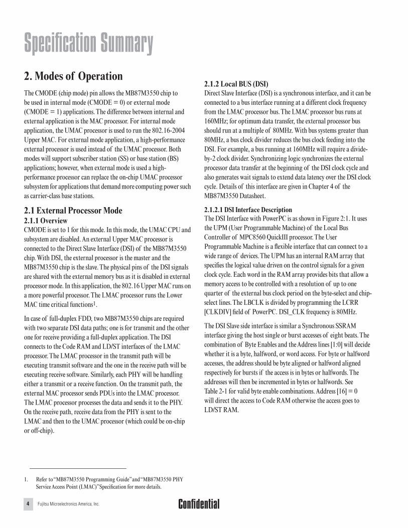
2. Modes of OperationThe CMODE (chip mode) pin allows the MB87M3550 chip to be used in internal mode (CMODE = 0) or external mode (CMODE = 1) applications. The difference between internal and external application is the MAC processor. For internal mode application, the UMAC processor is used to run the 802.16-2004 Upper MAC. For external mode application, a high-performance external processor is used instead of the UMAC processor. Both modes will support subscriber station (SS) or base station (BS) applications; however, when external mode is used a high-performance processor can replace the on-chip UMAC processor subsystem for applications that demand more computing power such as carrier-class base stations.
2.1 External Processor Mode2.1.1 OverviewCMODE is set to 1 for this mode. In this mode, the UMAC CPU and subsystem are disabled. An external Upper MAC processor is connected to the Direct Slave Interface (DSI) of the MB87M3550 chip. With DSI, the external processor is the master and the MB87M3550 chip is the slave. The physical pins of the DSI signals are shared with the external memory bus as it is disabled in external processor mode. In this application, the 802.16 Upper MAC runs on a more powerful processor. The LMAC processor runs the Lower MAC time critical functions1.
In case of full-duplex FDD, two MB87M3550 chips are required with two separate DSI data paths; one is for transmit and the other one for receive providing a full-duplex application. The DSI connects to the Code RAM and LD/ST interfaces of the LMAC processor. The LMAC processor in the transmit path will be executing transmit software and the one in the receive path will be executing receive software. Similarly, each PHY will be handling either a transmit or a receive function. On the transmit path, the external MAC processor sends PDUs into the LMAC processor. The LMAC processor processes the data and sends it to the PHY. On the receive path, receive data from the PHY is sent to the LMAC and then to the UMAC processor (which could be on-chip or off-chip).
2.1.2 Local BUS (DSI)Direct Slave Interface (DSI) is a synchronous interface, and it can be connected to a bus interface running at a different clock frequency from the LMAC processor bus. The LMAC processor bus runs at 160MHz; for optimum data transfer, the external processor bus should run at a multiple of 80MHz. With bus systems greater than 80MHz, a bus clock divider reduces the bus clock feeding into the DSI. For example, a bus running at 160MHz will require a divide-by-2 clock divider. Synchronizing logic synchronizes the external processor data transfer at the beginning of the DSI clock cycle and also generates wait signals to extend data latency over the DSI clock cycle. Details of this interface are given in Chapter 4 of the MB87M3550 Datasheet.
2.1.2.1 DSI Interface DescriptionThe DSI Interface with PowerPC is as shown in Figure 2:1. It uses the UPM (User Programmable Machine) of the Local Bus Controller of MPC8560 QuickIII processor. The User Programmable Machine is a flexible interface that can connect to a wide range of devices. The UPM has an internal RAM array that specifies the logical value driven on the control signals for a given clock cycle. Each word in the RAM array provides bits that allow a memory access to be controlled with a resolution of up to one quarter of the external bus clock period on the byte-select and chip-select lines. The LBCLK is divided by programming the LCRR [CLKDIV] field of PowerPC. DSI_CLK frequency is 80MHz.
The DSI Slave side interface is similar a Synchronous SSRAM interface giving the host single or burst accesses of eight beats. The combination of Byte Enables and the Address lines [1:0] will decide whether it is a byte, halfword, or word access. For byte or halfword accesses, the address should be byte aligned or halfword aligned respectively for bursts if the access is in bytes or halfwords. The addresses will then be incremented in bytes or halfwords. See Table 2-1 for valid byte enable combinations. Address [16] = 0 will direct the access to Code RAM otherwise the access goes to LD/ST RAM.
1. Refer to “MB87M3550 Programming Guide” and “MB87M3550 PHYService Access Point (LMAC)” Specification for more details.
4 Fujitsu Microelectronics America, Inc. Confidential

MB87M3550
Figure 2:1 PowerPC DSI Interface
Table 2-1: DSI Slave Interface
Byte Enables Access
1110110110110111
Byte access
11000011
Halfword access
0000 Word access
Any other combination
Word access
LB_CS#LBW/RD#
LB_CLK
LB_RDY#
AEC_EXT_IRQ#0
LB_DATA[31:0]
LB_ADDR[16:0]
LB_SIZE[2:0]
LB_BE#[3:0]
MB87M3550DSI SlavePowerPC
LCS0
LGPL3
LBCLK0
IINT0
LAD[0:31]
LGPL[2:0]
LBS[0:3]
LUPWAIT
LSYNC_OUT
LSYNC_IN
LATCH
Fujitsu Microelectronics America, Inc. 5Confidential

Specification Summary
2.1.2.2 DSI Pins
Table 2-2 Memory & External Device Interface
Name Type Drive Description
External Processor Mode:
LB_BE#[3:0] I/O 4mA Local Bus Byte Enables (Inputs). One bit per byte is used to indicate a valid data byte for host Read/Write accesses.
ECS#[5] = LB_CS#
I/O 4mA
LB_CS# (Input): Local Bus Chip Select. The Local Bus (DSI) is accessed only if “Chip Select” is asserted. Active low signal enables the interface for read/write operation.
ECS#[4] = LB_RDYMODE LB_RDYMODE (Input): Local Bus Ready Mode. Ready mode input is used for timing selection of presenting the valid data on the DSI Bus during a read operation after LB_RDY# asserted.
LB_RDYMODE = 0: As soon as LB_RDY# is asserted, then the valid data is available on the next rising edge of local bus clock (LB_CLK).
LB_RDYMODE = 1: As soon as LB_RDY# is asserted, then the valid data is available on the second rising edge of local bus clock (LB_CLK).
ECS#[3] = reserved
ECS#[2:0] = LB_SIZE[2:0] LB_SIZE[2:0] (Input): Local Bus Burst Size. The bus master asserts these pins to indicate that the current transaction is a burst transaction with variable burst sizes up to a maximum of eight words. Burst transfer can be performed in Byte or Words depending on LB_BE#[3:0] signals. If LB_SIZE[2:0] bits are zero, no burst is initiated.
LB_W/RD#I/O 4mA
Local Bus Read/Write Enable (Input). Active low signal enables read and active high signal enables write operation.
LB_RDY#I/O –
Local Bus Ready (Output). Upon a read access, this signal is asserted to indicate to the host processor when the data on the data bus is valid. The timing of presenting the valid data on the bus is based on LB_RDYMODE. For a write operation this signal is not used. For detailed timing refer to ARC subsystem description.
LB_DATA[31:0]I/O 4mA
Local Bus Data (I/O). Data bus bits 31-0 for the Local Bus (DSI) interface used by external host processor for data transfer between host and ARC Code RAM & Load/Store RAM. In write transactions, the bus master drives the valid data on this bus. In read transactions, the slave (ARC) drives the valid data on this bus.
LB_ADDR[16:0]I/O 4mA
Local Bus Address (Input). Address bus bits 16-0 for the Local Bus (DSI) interface used by external host processor to access the internal address space of ARC Code RAM (64Kbyte) & Load/Store RAM (32Kbyte). – Input Only.
External Processor Mode Only:
LB_CLKI
–Local Bus Clock. This clock is used for synchronous local bus (DSI) transactions between external host processor and ARC local memories. This clock is asynchronous with ARC internal clock and can support a maximum frequency of 80MHz.
6 Fujitsu Microelectronics America, Inc. Confidential

MB87M3550
2.1.3 External Processor ResponsibilitiesSince the UMAC CPU and subsystem are disabled, functions normally handled by the UMAC processor subsystem must be handled externally. Such functions include those handled by the following blocks:
• SPI
• I2C
• UMAC GPIO
• Power monitoring ADC
• AFC DAC
• Ethernet MAC
2.2 Normal ModeCMODE pin is set to 0 for this mode. In this mode, the on-chip UMAC CPU and its subsystem are used to run the 802.16 Upper MAC. External processor interface (DSI) is disabled.
2.3 System ApplicationThe MB87M3550 can be used in the following applications:
• BWA systems compliant with WiMAX
1. Residential CPEs (subscriber stations): Low-cost 802.16 subscriber stations.
2. Enterprise CPEs: High-throughput subscriber stations where an external MAC processor (Upper MAC) can be used to boost performance.
3. Base stations: For point-to-point or point-to-multi-point.
• Licensed and license exempt bands of 2–11GHz
• Independent frequency band suitable for 2.5, 3.5, 3.6 or 5.8GHz
• Half FDD/ full FDD or TDD applications
For full-duplex FDD applications two chips are required. For higher performance and more demanding base stations, an external processor can be used.
Complete reference designs are available for various purposes. The process toward certification by the WiMAX Forum is underway for the full-system version. This reference design includes all the software and hardware required for a cost-effective system solution2.
2. Refer to “MB87M3550 Application Guide” and “MB87M3550 SoC Reference Kit Manual” documents for system applications.
Fujitsu Microelectronics America, Inc. 7Confidential

Specification Summary
3. Reference Design 3.1 Hardware PlatformsSeveral hardware platforms are available with options for performing chip, software, and system verification. The Reference Board evaluation system for subscriber stations (Figure 3:1) can be configured to support either TDD or HDX FDD, depending on the radio selection.
This configuration can be suitable Subscriber Station TDD or HDX FDD applications.
Figure 3:2 provides an example of Reference Board configuration using an external processor. The simplified base station evaluation system of Figure 3:3 provides an example of a full duplex FDD implementation using an external processor.
The key features of the evaluation boards include:
• RF port interface for third-party radio
• Radio module
• Network interface
• On-board memory
• On-board control using SPI, I2C, and GPIO
• Debug port interfaces
• RS-232C interface port
• External power supply interface
Figure 3:1 TDD or HDX FDD Reference Board Evaluation System Using MB87M3550 Internal Processor
This configuration can be suitable for subscriber station TDD or HDX FDD applications.
FUJITSUMB87M3400
SOC
DDS
VCTCXO
Ethenet100/10 PHY
UMAC Debug Port
LMAC Debug Port
XfmrTemp.Sensor
RJ45
FLASH
SDRAM
Control
20 MHZ Ref -Clock
FS Clock
Clock
SPI
GPIO
RS-232C
RS232C
I2C
Power Module
ADC
ADC
DAC
DAC
ARX_I_IN +/ -
ARX_Q_IN +/ -
TX_Q Analog
TX_I Analog
RX & TX Pwr Detect
AGC Control
RF Logic Control
ADCADC
DACDAC
Radio Module
FUJITSUMB87M3550
SOC
DDS
VCTCXO
Ethenet100/10 PHY
UMAC Debug Port
LMAC Debug Port
XfmrTemp.Sensor
RJ45
FLASH
SDRAM
Control
20 MHZ Ref-Clock
FS Clock
Clock
SPI
GPIO
RS-232C
RS232C
I2C
Power Module
ADC
ADC
DAC
DAC
RX_I Analog
RX_Q Analog
TX_Q Analog
TX_I Analog
RX & TX Pwr Detect
AGC Control
RF Logic Control
ADCADC
DACDAC
SE7051L
Radio Module
SE7351L
8 Fujitsu Microelectronics America, Inc. Confidential

MB87M3550
Figure 3:2 TDD or HDX FDD Reference Board Evaluation System using External Processor
This configuration can be SS or BS for TDD or HDX FDD applications.
Figure 3:3 Example of a Full Duplex FDD Implementation
This configuration can be suitable for base station and backhaul applications.
DDSSPI
FS Clock Clock IN
Radio ModuleVCTCXO
Reference Board(External Processor Configuration)
PowerPCDebug Port
NetworkInterface
Temp.Sensor
FLASH
DDRSDRAM
I2CPowerPCMPS8560
PowerPC Module(MPC8560)
DSIFUJITSUMB87M3400
SOC
Power Module
DDSSPI
FS Clock Clock IN
Radio ModuleVCTCXO
Reference Board(External Processor Configuration)
PowerPCDebug Port
NetworkInterface
Temp.Sensor
FLASH
DDRSDRAM
I2CPowerPCMPS8560
PowerPC Module(MPC8560)
PowerPCDebug Port
NetworkInterface
Temp.Sensor
FLASH
DDRSDRAM
I2CPowerPCMPC8560
PowerPC Module(MPC8560)
DSIFUJITSUMB87M3550
SOC
Power Module
SE7351L SE7051L
DDS
OTCXO
FUJITSUMB87M3400
SOC
DDS ClockFS Clock
Clock
FUJITSUMB87M3400
SOC
FS Clock
Clock
DSI
RX Radio
TX Radio
PowerPCDebug Port
NetworkInterface
Temp.Sensor
FLASH
DDRSDRAM
I2C PowerPCMPS8560
PowerPC Module(MPC8560)
SPI ControlDDS
OTCXO
FUJITSUMB87M3550
SOC
DDS ClockFS Clock
Clock
FUJITSUMB87M3550
SOC
FS Clock
Clock
DSI
RX Radio
TX Radio
PowerPCDebug Port
NetworkInterface
Temp.Sensor
FLASH
DDRSDRAM
I2C PowerPCMPS8560
PowerPC Module(MPC8560)
PowerPCDebug Port
NetworkInterface
Temp.Sensor
FLASH
DDRSDRAM
I2C PowerPCMPC8560
PowerPC Module(MPC8560)
SPI Control
Fujitsu Microelectronics America, Inc. 9Confidential

Specification Summary
3.2 Software PlatformThe Fujitsu 802.16 software platform implements a subscriber station or base station with the following features:
• Compliance with IEEE 802.16-2004 standard specification
• MAC security sublayer for subscriber station authentication and data encryption
• Multiple service class support to differentiate service quality
• Dynamic service management to activate service class when needed
• MAC portability to different RTOSs
The typical 802.16 software platform available from Fujitsu contains the following components:
• Host software (runs on either the on-chip UMAC or external processor) with the following subcomponents:
1. Board support packages (BSPs) for popular operating systems
2. RTOS wrapper
3. Device drivers, such as Ethernet, IIC, SPI, UART, etc.
4. BS or SS management and application
5. 802.16 upper layer MAC
• 802.16 PHY service access point and lower layer MAC (PSAP/LMAC) firmware (runs on the on-chip LMAC processor)
As shown in an overview of Fujitsu’s software platform (Figure 3:4), the 802.16 upper layer MAC accesses the OFDM PHY through PSAP/LMAC firmware running on the on-chip LMAC processor. In addition to providing PHY access primitives, the PSAP/LMAC firmware includes some 802.16 lower layer MAC functionality to offload tasks from the upper layer MAC. This functionality includes encryption/decryption engines and a CRC checker/inserter.
Fujitsu provides the BSP and device drivers for the supported operating systems, as well as the RTOS wrapper, thus simplifying the porting of the complete software suite to any operating system supported by Fujitsu. Fujitsu’s 802.16 upper layer MAC can also be replaced with a third-party component. Fujitsu provides full API and interface specifications to enable third parties to develop upper layer MAC components.
Fujitsu also provides the PSAP/LMAC firmware for BS and SS applications. The upper layer MAC coupled with the PSAP/LMAC firmware make up the complete 802.16 protocol stack.
Figure 3:4 Fujitsu Software Architecture
MB87M3550 BS or SS Management
RTOS API
RTOSWrapper
RTOS
TCP/UDP/IP
Ethernet Driver
Bridge
802.16 Upper MAC
802.16 Lower MAC
OFDM PHYIP Network
Other Device Drivers
Network API MAC Management API
10 Fujitsu Microelectronics America, Inc. Confidential

MB87M3550
3.2.1 Software Functional OverviewThe following Figure shows major tasks implemented in Upper MAC (UMAC) and in Lower MAC (LMAC):
Figure 3:5 MAC Partitioning
A brief overview of PSAP/LMAC is provided in the following sub-sections. Details of PSAP/LMAC can be found in the Fujitsu MB87M3550 PHY Service Access (LMAC) Specification. This specification has been developed to support UMAC development.
The PSAP/LMAC has 3 main operational modes: IDLE, SCAN and RUN. Each of these modes are briefly explained in the following sections. Note: In the description that follows, [SS] implies that the description applies to Subscriber Station only, [BS] implies that the description applies to Base Station only, and [SS] [BS] imply that the description applies to both SS, and BS.
3.2.1.1 IDLE Mode [SS] [BS]IDLE is the first mode automatically entered right after the startup. Upon boot-up the PSAP/LMAC initializes and starts waiting in the IDLE mode. The PSAP/LMAC sends a message (through the messaging system) to the UMAC to indicate the arrival at the IDLE mode. In the IDLE mode, PSAP/LMAC does not pass traffic. It only processes messages sent by the UMAC through the messaging system. Messaging System is explained in more detail in the Fujitsu MB87M3550 PHY Service Access (LMAC) Specification.
3.2.1.2 SCAN Mode [SS]The SCAN mode exists only for SS operation and it is for initial synchronization to a BS. The information is provided by the PSAP/LMAC to the UMAC during the SCAN mode to support the initial network entry process. The PSAP/LMAC can be put in the SCAN mode by the UMAC using a mode change message, through the messaging system. Before starting the SCAN mode, the UMAC can optionally initialize various parameters, such as CP length, frame length, etc., if known, via messages sent through the messaging system. In SCAN mode, an attempt to locate and synchronize with a service is made. During the SCAN mode, PSAP/LMAC continuously sends status indicators and data to the UMAC, to support the initial ranging process running on the UMAC. Upon successfully locating and synchronizing to a service, the PSAP/LMAC has to be switched to the RUN mode by the UMAC using a mode change message. This not only terminates the SCAN mode but also starts the RUN mode, where full data traffic is delivered by PSAP/LMAC in both directions. The SCAN mode is not available for BS operation [BS].
• Bridge between UMAC and the PHY
• Isolates PHY complexity from UMAC
• Programmable / flexible solution
• Off-loads the burden from UMAC by performing:
• Data encryption and decryption
• CRC and HCS generation / checking
• CID based filtering
• Transmission convergence sublayer
• PDU classification and FEC block processing
• Provides PHY access primitives
• Different versions for BS and SS
Lower Layer MAC Software (LMAC)
PHY Service Access Point
• Implemented on either internal or external network processor
• Provides higher level 802.16 MAC functionality
• MAC management
• Service specific convergence sublayers
• Common part sublayer
• Key management
• Different versions for BS and SS
• BS version is likely to run on a more powerful processor
Upper Layer MAC Software (UMAC)
Fujitsu Microelectronics America, Inc. 11Confidential

Specification Summary
3.2.1.3 RUN Mode [SS] [BS]This is the normal operating mode for the PSAP/LMAC. In the RUN mode, the PSAP/LMAC actually transfers traffic between the UMAC and the OFDM PHY. The RUN mode can be terminated by the UMAC by a mode change message, putting the PSAP/LMAC into either the IDLE mode or the SCAN mode again. In SS, RUN mode can be entered only after a successful SCAN mode completion and upon a mode change message from the UMAC [SS]. In BS, the SCAN mode does not exist and the UMAC must switch the PSAP/LMAC to RUN mode from the IDLE mode by a modechange message [BS].
3.2.2 Data and Control InterfaceThe data and control exchange between the UMAC and the PSAP/LMAC is handled through separate flows. The traffic burst data and associated control flow utilizes several buffers and data structures allocated in the shared memory section. These flows are explained in detail in the “PHY Service Access Point (LMAC) Interface Specification”. The non-traffic communication between the UMAC and the PSAP/LMAC use a special messaging scheme. The special messaging system is considered as a part of control interface and explained thoroughly in the “PHY Service Access Point (LMAC) Interface Specification”. The main elements of the UMAC-PSAP/LMAC interface are shown in Figure 3:6.
Figure 3:6 UMAC-PSAP/LMAC Data and Control Interface Elements
IP
OP
MAC_RX_BUFFER
RX Watermark
MAC PDUs
IP
OP
TX Watermark
MAC PDUs
Measuring Structure
UMACMailbox
PSAPMailbox
DMC
TEK Table
CID Table
IP
OP
RX_STAT_BUFFER
RSIs and RSIPs
IP
OP RBCTs
RX_CTRL_IP
OP
TX_CTRL_BUFFER BUFFER
TCTs
DIUC Tables
Control Block(contains all direct access
registers)
MAC_TX_BUFFER
12 Fujitsu Microelectronics America, Inc. Confidential

MB87M3550
There are 2 pointers for each circular buffer, as shown in Figure 3:6, the input pointer (IP) and the output pointer (OP). These pointers are used for data insertion and retrieval from the associated buffer. Whenever new data is to be inserted into a buffer, it is inserted to the
location pointed by IP. Similarly, data is retrieved from the location pointed by OP. The following figures show the series of events on data and control interfaces in a typical transmission and reception for BS and SS.
Figure 3:7 Data and Control Sequence for a Typical Transmission [SS] [BS]
Figure 3:8 Base Station Data and Control Sequence for a Typical Reception [BS]
Write Tx data and update IP
Write TCT andupdate IP
Read TCT and update OP
Read Tx data and update OP
PSAPdetects thepointerupdate
UM
AC
TX
_CT
RL_
BU
FF
ER
MA
C_T
X_B
UF
FE
R
RX
_CT
RL_
BU
FF
ER
RX
_ST
AT
_BU
FF
ER
MA
C_R
X_B
UF
FE
R
PS
AP
Write RBCT and update IP
Upon RXHIGH interrupt, read RSI and RSIPs for the incoming burst and update OP
Read RBCT and update OP
Read Rx data and update OP
Write Rx data,update IP and issueRXHIGH interrupt
Write status info (RSI and RSIPs) for theincoming burst and update IP
UM
AC
TX
_CT
RL_
BU
FF
ER
MA
C_T
X_B
UF
FE
R
RX
_CT
RL_
BU
FF
ER
RX
_ST
AT
_BU
FF
ER
MA
C_R
X_B
UF
FE
R
PS
AP
Fujitsu Microelectronics America, Inc. 13Confidential

Specification Summary
Figure 3:9 Subscriber Station Data and Control Sequence for a Typical Reception [SS]
3.2.2.1 UMAC-PSAP/LMAC Data InterfaceThe elements constituting the UMAC-PSAP/LMAC data interface are:
• UMAC Transmit Buffer (MAC_TX_BUFFER)
• UMAC Receive Buffer (MAC_RX_BUFFER)
• TX and RX Watermarks
• IPs and OPs to the above buffers
• Watermark Interrupts
The following figure depicts the basic data flow and associated interrupts during typical data flow between the PSAP/LMAC and the UMAC.
Figure 3:10 PSAP/LMAC-UMAC Data Interface
Upon RXHIGH interrupt, read status info (RSI and RSIPs) for the incoming burst and update OP
Read Rx data and update OP
Write Rx data,update IP and issueRXHIGH interrupt
Write status info (RSI and RSIPs) for the incoming burst and update IP
UM
AC
TX
_CT
RL_
BU
FF
ER
MA
C_T
X_B
UF
FE
R
RX
_CT
RL_
BU
FF
ER
RX
_ST
AT
_BU
FF
ER
MA
C_R
X_B
UF
FE
R
PS
AP
UMAC PSAP
MAC_TX_BUFFER
MAC_RX_BUFFER
Tx Data Flow Tx Data Flow
Rx Data Flow Rx Data Flow
Tx Low Watermark Interrupt
Rx High Watermark Interrupt
14 Fujitsu Microelectronics America, Inc. Confidential

MB87M3550
There are 2 interrupts associated with the flow of data between the PSAP/LMAC and the UMAC. TX Low Watermark Interrupt is issued by the PSAP/LMAC when the low watermark has been reached in the MAC_TX_BUFFER and the UMAC should write more data to the MAC_TX_BUFFER. RX High Watermark Interrupt is issued by the PSAP/LMAC when the high watermark has been reached in the MAC_RX_BUFFER and the UMAC should collect data from the MAC_RX_BUFFER. Watermark levels can be set by the UMAC using the messaging system.
3.2.2.2 UMAC-PSAP/LMAC Control InterfaceThe elements constituting the UMAC-PSAP/LMAC control interface are:
• Transmit Control Buffer (TX_CTRL_BUFFER)
• Receive Control Buffer (RX_CTRL_BUFFER) [BS]
• Receive Status Buffer (RX_STAT_BUFFER)
• IPs and OPs to the above buffers
The following figure depicts the basic control flow and associated interrupts during the typical operation of the PSAP/LMAC and the UMAC.
Figure 3:11 PSAP/LMAC-UMAC Control Interface
PSAPUMAC
TX_CTRL_BUFFER
RX_CTRL_BUFFER
TCT TCT
RBCT [BS] RBCT [BS]
RX_STAT_BUFFERRSI, RSIP RSI, RSIP
Messaging SystemMAILBOXES
message message
Messaging System Interrupts
MESSAGING SYSTEM
Fujitsu Microelectronics America, Inc. 15Confidential

Specification Summary
3.3 Reference Design KitThe Reference Board is shown in Figure 3:12. Contents of the Reference Kit are shown in Figure 3:13.
Figure 3:12 Reference Board Photo
The Reference Board of Figure 3:12 shows:
• SS Reference Board with RF board • BS Reference Board (TDD or FDD) with Power-PC interface and RF board
Figure 3:13 What Is Included in the Reference Kit?
SoC Reference Board RF Board SoC Debugger Board
Serial Port Cable
Power Supply MCX Cables
Power Cable
SoC Baseband Board
16 Fujitsu Microelectronics America, Inc. Confidential

MB87M3550
4. SoC Top-Level Signals and Signal GroupsA signal group is shown in Figure 4:1 below for internal processor mode.3Figure 4:1 Functional Signal Group Diagram (Internal Processor Mode)
3. See MB87M3550 Datasheet for full description of the signals.
MB87M3550SOC
(InternalProcessor Mode)
SD_RAS#SD_CAS#SD_WE#SD_CLKSD_CKE
SD_DQM[3:0]/EWE#[3:0]ECS#[5:0]
ERE#EALEERDY
EDATA[31:0]EADDR[25:0]
BOOT[1:0]
AGC_CTRL[9:0]AGC_STROBE
LD#LD
RX_ENTR_SW
BS_SYNC_INBS_SYNC_OUT
RX_PWR_DETECTTX_PWR_DETECT
FT_INT
ATX_I_OUT-DTX_I_OUT[9:0]
ATX_Q_OUT-
DTX_Q_OUT[9:0]
ARX_I_IN+
TX_EN
ARX_I_IN-DRX_I_IN[[9:0]ARX_Q_IN+ARX_Q_IN-DRX_Q_IN[9:0]
ADC_DAC_CLK
SED_OUT_CLKSED_OUT_DATASED_OUT_FS
ExternalMemoryInterface
MII_TXD[3:0]MII_TXENMII_TXER
MII_TXCLKMII_RXD[3:0]
MII_RXDVMII_RXER
MII_RXCLKMII_COLMII_CRSMII_MDC
MII_MDIOMII_LINK#
MII_FD#MII_100M#
Ethernet PHYInterface
Peripherals &InterruptsInterface
SPI_DISPI_DO
SPI_CLKSPI_CS[1:0]#
SDASCL
UART_TXDUART_RXD
UMAC_GPIO[24:0]UMAC_EXT_IRQ[1:0]
LMAC_GPIO[3:0]LMAC_EXT_IRQ#[1:0]
DDS_CLK_OUTSAMPL_CLK_2X
PWR_RESET#
CMODE
REFCLK1PLL1_S
PLL1_SPEED[1:0]PLL1_VDDPLL1_VSS
REFCLK2PLL2_S
PLL2_SPEED[1:0]PLL2_VDDPLL2_VSS
REFCLK3PLL3_S
PLL3_VDDPLL3_VSS
EXT_RESET#
VPD
VCTCXO_CNTL
Clocks&
Reset
PLL3_SPEED
LMAC DebugPort
RadioInterface
UMAC DebugPort
JTCKJTDIJTMSJTRSTJTDO
JTAGBoundary
Scan
Digital 3.3VDigital 1.8V
Analog 3.3VAnalog 1.8V
Digital GroundPower
Analog Ground
ADC2_VRHADC2_VRLADC2_VR
DAC_I_VRODAC_I_VREFDAC_I_COMP
ADC_I&Q_VRHADC_I&Q_VRLADC_I&Q_SG
DAC2_VRHDAC2_VRL
VoltageReferences
RF_ENABLE
DAC_Q_COMP
ADC_I&Q_VREF
MII_conn
LBCLK (for BS Mode)
PTEST
ATX_Q_OUT+
ATX_I_OUT+
Fujitsu Microelectronics America, Inc. 17Confidential

MB87M3550
Signals used in external mode are shown in Figure 4:2 below:Figure 4:2 Functional Signal Group Diagram (External Processor Mode)
Certain pins of the SoC are shared and have different meanings in external and internal processor modes. Table 4-1 shows pins that are shared for the two modes.
Table 4-1 Shared Signals for Different Modes of Operation
Internal Processor Mode External Processor Mode
ECS#[5] LB_CS#
ECS#[2:0] LB_SIZE[2:0]
EWE[3:0] LB_BE#[3:0]
EADDR_L[16:0] LB_ADDR[16:0]
ECS#[4] LB_RDYMODE
ERE# LBW/RD#
ERDY LB_RDY#
EDATA[31:0] LB_DATA[31:0]
MB87M3550SOC
(ExternalProcessor Mode)
LB_CLKLB_SIZE[2:0]LB_BE#[3:0]
LB_CS#LB_W/RD#
LB_RDYMODELB_RDY#
LB_DATA[31:0]LB_ADDR[16:0]
AGC_CTRL[9:0]AGC_STROBE
LDLD#
RX_ENTR_SW
ATX_I_OUT+
DTX_I_OUT[9:0]
ATX_Q_OUT-DTX_Q_OUT[9:0]
ARX_I_IN+
TX_EN
ARX_I_IN-DRX_I_IN[[9:0]ARX_Q_IN+ARX_Q_IN-DRX_Q_IN[9:0]
ADC_DAC_CLK
SED_OUT_CLKSED_OUT_DATASED_OUT_FS
Local BusDSI
Interface
LMACInterrupts &
GPIO
LMAC_GPIO[3:0]LMAC_EXT_IRQ#[1:0]
DDS_CLK_OUTSAMPL_CLK_2X
PWR_RESET#
CMODE
REFCLK3PLL3_S
PLL3_VDDPLL3_VSS
EXT_RESET#
VPD
Clocks&
Reset
PLL3_SPEED
LMACDebugPort
RadioInterface
Digital 3.3VDigital 1.8V
Analog 3.3VAnalog 1.8V
Digital Ground
Power
Analog Ground
DAC_I_VRODAC_I_VREFDAC_I_COMP
ADC_I&Q_VRHADC_I&Q_VRLADC_I&Q_SG
VoltageReferences
RF_ENABLE
DAC_Q_COMP
ADC_I&Q_VREF
JTCKJTDIJTMSJTRSTJTDO
JTAGBoundary
Scan
BS_SYNC_INBS_SYNC_OUTFT_INT
ATX_Q_OUT+
ATX_I_OUT-
PTEST
REFCLK2PLL2_S
PLL2_SPEED[1:0]PLL2_VDDPLL2_VSS
Fujitsu Microelectronics America, Inc. 18Confidential

MB87M3550
5. Operating Conditions and Electrical Specification5.1 Digital Characteristics5.1.1 Absolute Maximum RatingsTable 5-1: Absolute Maximum Ratings
The device can be permanently damaged by application of stress (voltage, current, temperature, etc.) in excess of the absolute maximum ratings.
5.1.2 Recommended Operating Conditions
Table 5-2: Recommended Operating Conditions
Notes: Recommended operating conditions are normal operating ranges for the device. All the device’s electrical characteristics are guaranteed when operating within these ranges. Always use the device within these recommended operating conditions. Operation outside these ranges may adversely affect reliability and could result in device failure.
5.1.3 DC CharacteristicsMeasurement Conditions: over recommended operating conditions
Table 5-3: DC Characteristics
5.1.4 AC Characteristics and MeasurementsAC characteristics are determined based on junction temperature, supply voltage, and process variations. Table 5-4 shows the variation of AC characteristics under the recommended operating conditions.
Table 5-4: AC Characteristics Variation
Symbol Description Value Unit
VDDI Internal Core Power Supply Voltage -0.5 to 2.5 V
VDDE External IO Power Supply Voltage -0.5 to 4.0 V
VI Input Voltage -0.5 to VDDE + 0.5 V
VO Output Voltage -0.5 to VDDE + 0.5 V
IO Output Current (Average DC Current) ±4 mA
Tst Storage Temperature -55 to 125 °C
Tj Junction Temperature -40 to 125 °C
Symbol Description Min. Typ. Max. Unit
VDDIInternal Power Supply Voltage
1.65 1.8 1.95 V
VDDEExternal IO Power Supply Voltage
3.0 3.3 3.6 V
VIH Input High Voltage 2.0 – VDDE + 0.3 V
VIL Input Low Voltage -0.3 – 0.8 V
Tj Junction Temperature -40 125 °C
Symbol Description Conditions Min. Typ. Max. Unit
VIL Input Low Voltage VDDE = 3.0 -0.3 — 0.8 V
VIH Input High Voltage 2.0 — VDDE + 0.3 V
VOL Output Low Voltage3.3V Output
IOL = 100µA0 — 0.2 V
VOH Output High Voltage3.3V Output
IOH = 100µAVDDE – 0.2 — VDDE V
ILI Input Leakage Current VDDE = 3.6 V — — ±4 µA
ICC1 VDDI Supply Current 100MHz Clock TBD
Power Down TBD
ICC2 VDDE Supply Current 100MHz Clock TBD
Power Down TBD
RP Pull up/Pull down Resistor 10 33 80 kΩ
Symbol Conditions Delay (ns)
tpd(max) Tj = 125°C, VDDI = 1.65 V, VDDE = 3.0 V ttyp x 1.58
tpd(typ) Tj = 25°C, VDDI = 1.80 V, VDDE = 3.3 V ttyp x 1.00
tpd(min) Tj = -40°C, VDDI = 1.95 V, VDDE = 3.6 V ttyp x 0.64
Fujitsu Microelectronics America, Inc. 19Confidential

Specification Summary
The measurements are performed with load capacitance of 30 pF. The equivalent buffer circuit is given in Figure 6:1. The AC measurement parameters are shown in Figure 6:2 with following conditions:Figure 5:1 Equivalent Circuits for AC Measurements
Figure 5:2 AC Measurements
5.1.5 Input/Output Pin CapacitanceInput/output pin capacitance is given in Table 6-5.
The measurement conditions are: Tj = 25°C, VDD = VI = 0 V, f = 1MHz.
Table 5-5: IO Pin Capacitance
Measurement SW1 SW2
L → H, H → L OFF OFF
L → Z, Z → L ON OFF
H → Z, Z → H OFF ON
VDD
VSS
Measuring Pin
I = 1.65mA
I = 1.65mA
SW1
SW2C
Device Output Pin
80%20%
80%
tr
tpHL
tpZL tpLZ
tpZH tpHZ0.5V
0.5V
tpLH
Input
VDD/2
(VLH + VIL)/2
VDD/2
VDD/2
VDD/2
Output
Output enable
Output disable
tf
20%
Symbol Conditions Maximum Unit
CIN Input Pin 16 pF
COUT Output Pin 16 pF
CI/O I/O Pin 16 pF
20 Fujitsu Microelectronics America, Inc. Confidential

MB87M3550
6. Package Mechanical Information436 Face Down Heat-Spreader Ball Grid Array Package (436 FDHBGA). Note: The SoC will use lead free package and is RoHS compliant.Fujitsu Microelectronics America, Inc. 21Confidential

Specification Summary
7. Supporting DocumentsThe following documents have been developed to support systems based on the MB87M3550 SoC. Note that many of these documents require an NDA.7.1 Web Access DocumentsThe following Web site is a good resource for initial documents:
http://www.fujitsu.com/us/services/edevices/microelectronics/broadbandwireless/
• Product Fact Sheet/Product Brief• Presentation• White papers• Press releases• Documentation• FAQ
7.2 Documents for System Development The following documents have been developed to support systems based on MB87M3550 SoC.
Table 7:1 NDA Documents
Fujitsu WIMAX SoC Document List for System Development
Document Number
Document Title Access Description
00 FUJITSU WIMAX SOC Presentation NDA Introduction to FUJITSU WIMAX 802.16-2004 SoC.
01Fujitsu WiMAX 802.16-2004 SoC MB87M3550 Datasheet
NDAIntroduction, Detailed Features, Pin Description, Description of Internal Sub-systems (Block Diagrams, Memory Map, Register Map Timing Diagrams), Description of Clocks, Power Monitoring, Description of RF interface ADC/DAC, Electrical Characteristics.
02Fujitsu WiMAX 802.16-2004 SoC MB87M3550 Programming Guide
NDAIntroduction to MB87M3550 Software Components, functional description of Software modules, partitioning of MB87M3550 Software into Upper MAC (UMAC) and Lower MAC (PSAP) components. Note: PSAP → PHY Service Access Point and there is a separate document that describes PSAP in detail.
03Fujitsu WiMAX 802.16-2004 SoC MB87M3550 PHY Service Access Point (PSAP)
NDADetails for UMAC developer to interface with Fujitsu's embedded PSAP/LMAC, Description of PSAP/LMAC functions, Description of data and control structures, description of operating modes, network entry and typical operation
04Fujitsu WiMAX 802.16-2004 SoC MB87M3550 Application Guide
NDA
Application notes and guidelines containing details of how to use MB87M3550 at the system level, describes system bandwidth, clock, DDS, Sampling Frequency requirements, describes system memory interface for FLASH, SDRAM, Describes internal and external modes (with PowerPC example), contains details of Radio Interface, AGC, AFC, examples of VOIP, T1/E1 applications, contains answers to a number of Frequently Asked Questions (FAQ), Test results and performance data (from SUI Channel model simulations and RF Perfor-mance tests for BPSK, QPSK, QAM-16 and 64-QAM).
05 Fujitsu WiMAX 802.16-2004 MB87M3550 SoC Reference Kit
NDAThe document describes the necessary Hardware and Software components to develop a cost effective, fixed Broadband Wireless Access (BWA) system solution for Subscriber Station (low-cost), Enterprise SS, and Base Stations.
06 SiGe Radio Documentation NDA
• RF chipset datasheet • RF board specification• Schematics, layout guide and BOM• Performance dataNote: RF chip technical support will be provided from RF chip companies, not from Fujitsu. Contact information will be provided separately.
07 PowerPC MPC8560 Documentation NDA• Hardware reference manual• Schematics and BOM
22 Fujitsu Microelectronics America, Inc. Confidential

MB87M3550
After an NDA is in place, the following documents may be provided from the above list:• Fujitsu WiMAX SoC presentation (Document #00)
• The Fujitsu WiMAX 802.16-2004 SoC Datasheet (Document #01)
• The Fujitsu WiMAX 802.16-2004 SoC Programming Guide (Document #02)
Following information will only be provided to enable customers to make business decision on Fujitsu.
• The Fujitsu WiMAX 802.16-2004 SoC PHY Service access Point (LMAC) Interface Specification for UMAC Developers* (Document #03)
• The Fujitsu WiMAX 802.16-2004 SoC Application Guide (Document #04)
• The Fujitsu WiMAX 802.16-2004 SoC Reference Kit (Document #05)
• SiGe RF board Documentation (Document #06)
• PowerPC MPC8560 Board Documentation (Document #07)
*Only for customers who develop their own upper MAC.
Fujitsu Microelectronics America, Inc. 23Confidential

Specification Summary
24 Fujitsu Microelectronics America, Inc. Confidential
8 Certification and ComplianceFujitsu has designed the MB87M3550 wireless MAN SoC to comply with the IEEE 802.16-2004 standard and intends to certify systems according to WiMAX profiles.
For more informationMore information on the IEEE 802.16 standard for broadband wireless access and the WiMAX Forum is available at www.wimaxforum.org and www.ieee802.org/16.
For more information on Fujitsu’s broadband wireless SoC, please address e-mail to [email protected].
WiMAX Forum is a trademark of the WiMAX Forum. All other product names and company names mentioned herein are the trademarks or registered trademarks of their respective firms.

FUJITSU MICROELECTRONICS AMERICA, INC.Corporate Headquarters1250 East Arques Avenue, M/S 333, Sunnyvale, California 94088-3470Tel: (800) 866-8608 Fax: (408) 737-5999E-mail: [email protected] Web Site: http://us.fujitsu.com/micro
©2006 Fujitsu Microelectronics America, Inc. All rights reserved.
All company and product names are trademarks or registered trademarks of their respective owners.
Printed in U.S.A.
BWA-DS-21197-7/2006Confidential
Revision History:
Rev Date Authors Description
1.0 7/12/06 SA Release 1.0