the development of multi level buck converter …umpir.ump.edu.my/id/eprint/4864/1/cd6749_89.pdf ·...
TRANSCRIPT
THE DEVELOPMENT OF MULTI LEVEL BUCK CONVERTER
MUHAMMAD FARHAN BIN KAMARUL ZAMAN
This thesis is submitted as partial fulfillment of the requirements for the
award of the Bachelor of Electrical Engineering (Power System)
Faculty of Electrical & Electronics Engineering
University Malaysia Pahang
JUNE 2012

vi
ABSTRACT
A DC/DC converter generally needs to work under high switching frequency
when used as an adjustable power supply to reduce the size of magnetic elements
such as inductors, transformers and capacitors, but with the rising of the switch
frequency, the switch losses will increase and the efficiency will reduce. To solve
these problems, research is actively being done on a soft switching method that can
be applied under high frequency and on a PWM converter that can be applied under
low frequency such as a multi level topology. In this project, a DC-DC conversion
method for reducing the ripple of output voltage is proposed. In this proposed
converter, buck converters are connected in series to generate the output voltage. By
using this method, the ripple of output voltage can be reducing compared to a
conventional buck converter. Particularly when output voltage is low, the number of
acting switching elements is less and the result of ripple reduction is more obvious, it
is expected that the converter proposed in this project could be very useful in the case
of wide-range output voltage.
vii
ABSTRAK
Penukar DC / DC umumnya diperlukan untuk bekerja di bawah frekuensi
pensuisan yang tinggi apabila digunakan sebagai bekalan kuasa boleh laras bagi
mengurangkan saiz unsur-unsur magnet seperti indukter, transformer dan kapasitor,
tetapi dengan peningkatan kekerapan suis, kerugian suis akan meningkat dan
kecekapan akan berkurang. Bagi menyelesaikan masalah-masalah ini, penyelidikan
sedang giat dilakukan pada kaedah pensuisan yang lembut bagi membolehkan ia
diguna pakai di bawah frekuensi tinggi dan pada penukar PWM yang boleh
digunakan di bawah frekuensi rendah seperti topologi tahap yang berbilang. Dalam
projek ini, satu kaedah DC-DC penukar untuk mengurangkan riak voltan keluaran
adalah dicadangkan. Dalam penukar yang dicadangkan ini, penukar buck disambung
secara siri untuk menjana voltan keluaran. Dengan menggunakan kaedah ini, riak
voltan keluaran boleh dikurangkan berbanding dengan penukar buck konvensional.
Terutamanya apabila voltan keluaran adalah rendah, bilangan yang bertindak
menukar unsur-unsur kurang dan hasil pengurangan riak lebih jelas, ia dijangka
bahawa penukar yang dicadangkan dalam projek ini menjadi sangat berguna dalam
kes voltan keluaran jarak lebar.

viii
TABLE OF CONTENTS
CHAPTER CONTENTS PAGE
DECLARATION ii
DEDICATION iv
ACKNOWLEDGEMENT v
ABSTRACT vi
ABSTRAK vii
TABLE OF CONTENT viii
LIST OF TABLES x
LIST OF FIGURES xi
LIST OF ABBREVIATION xiii
LIST OF APPENDICES xiv
1 INTRODUCTION 1
1.1 Background of the Project 1
1.2 Problems Statement 2
1.3 Objectives 2
1.4 Scope of Project 3
2 LITERATURE REVIEWS 4
2.1 Introduction 4
2.2 Buck Converter 4
2.3 Multi-level Conversion Method 8

ix
2.4 Control Scheme 10
2.4.1 Voltage Mode Control 11
2.4.2 Current Mode Control 12
3 METHODOLOGY 15
3.1 Project Procedure 15
3.2 Buck Converter Design 17
3.3 Simulation of Multi-level Buck Converter 19
4 HARDWARE DEVELOPMENT 22
4.1 Power stage 22
4.1.1 Power Switch 22
4.1.2 Power Diode 23
4.1.3 Output Capacitor 23
4.1.4 Inductor 24
4.1.5 Input Capacitor 24
4.1.6 Load 24
4.2 Controller Stage 25
4.3 MOSFET Driver Circuit 26
5 RESULT AND DISCUSSIONS 30
5.1 Simulation Result 30
5.2 Experimental Result 33
6 CONCLUSION AND RECOMMENDATIONS 36
6.1 Conclusion 36
6.2 Recommendations 37
REFERENCES 38
APPENDICES 39
x
LIST OF TABLE
TABLE NO. TITLE PAGE
3.1 Specification of Buck Converter 17
xi
LIST OF FIGURES
FIGURE NO TITLE PAGE
2.1 Buck converter 5
2.2 Inductor’s Voltage Waveform 5
2.3 Inductor’s Current waveform 7
2.4 Capacitor’s Current waveform 8
2.5 Proposed multi-level DC/DC Converter 9
2.6 Block Diagram for Feedback Control 11
2.7 Signal Pulse Width Modulator 12
2.8 Current Mode Control Block Diagram 13
3.1 Flow Chart of Methodology 16
3.2 (a) 1st Level Buck Converter circuit 19
(b) 2nd
Level Buck Converter Circuit
3.3 Feedback Control of Buck Converter 21
4.1 UC3825N Circuit Diagram 25
4.2 (a) Opto-isolater Block Diagram 27
(b) 6N137 Block Diagram
4.3 (a) MC34151 Pin Connection 28
(b) MC34151 Block Diagram

xii
4.4 MOSFET Driver Circuit 29
5.1 (a) Output Voltage of 1st level 31
(b) Output Voltage of 2nd
level
5.2 (a) Comparison between error signal 32
(b) Signal PWM
5.3 PWM circuit diagram using UC3825N 33
5.4 (a) Sawtooth waveform and reference Voltage 34
(b) PWM waveform
5.5 Output Waveform from the driver circuit 35
5.6 Voltage Output From Buck Converter 35
xiii
LIST OF ABBREVIATIONS
DC Direct Current
CCM Continues Conduction Mode
VMC Voltage Mode Control
PWM Pulse Width Modulation
MOSFET Metal Oxide silicon Field Effect Transistor
BJT Bipolar Junction Transistor
RDS (on) Static Drain-Source on Resistor
VDSS Drain to Source Voltage
ESR Equivalent Series Resistor
IC Integrated Circuit
xiv
LIST OF APPENDIX
APPENDIX TITLE PAGE
A1 Power stage 39
A2 VMC controller 39
A3 MOSFET driver 40
A4 The project with VMC controller 40
B UC3825N datasheet 41
C IRF540N datasheet 50
D MC34151 datasheet 58
E 6N137 datasheet 67
CHAPTER 1
INTRODUCTION
1.1 Background of the Project
The DC-DC converter is a type of power converter in power electronic is
the circuits that convert the voltage from one DC to another DC level. Power
electronics are become importance device in the world, which is widely used to
control and conversion electrical power. In general, DC to DC converters are widely
used at home and industries to produce the desired output power. The converter
devices are uses in a variety applications for the power ranging from watt (mobiles
phones), kilowatts (dc motor drives) to megawatts (vehicles). There are many types
of dc-dc converter like buck converter, boost converter, buck-boost converter and etc
in power electronics. With these converters, they can perform different types of
applications: step-down of voltage, step-up, inversion of polarity, and conversion of
dc to dc or vice versa.
A DC to DC converter usually works under high frequency to reduce the size
of inductors, transformers, capacitors and so on. However, the higher the switching
frequency, the more losses suffered, which result in a new problem of efficiency
reduction. Recent studies mainly focus on two fields: one is on software switching
methods to reduce the losses of switching under high working frequency conditions
and the other is on the structure of multi-level converter under low frequency
working conditions.

2
In this project, a multi-level DC to DC conversion method is presented to
reduce the output voltage ripple of DC-DC converters. The proposed converter
producing multi-voltage is made of buck converter in series, which reduces the ripple
of output voltage compared to traditional buck converters. Furthermore, the number
of acting switch elements will be reduced when the output voltage is lower, so that
the multi-level DC/DC conversion method has a special advantage under lower
output voltage. The proposed converter is especially for application to wide range
output.
1.2 Problems Statement
There are a lot of procedures in designing and implementing the multi level
DC-DC buck converter. These involved a procedure from specification of converter,
circuit topology selection, simulation to validate the design, components selection
and lastly hardware implementation. Although the simulation gives a desired result,
there are still gaps between theoretical principle and practical accomplishment. This
happens because in theory, the calculation is done by making assumptions which can
simplify or make the analysis. However, the hardware will be designed by observing
the previous projects or research. The entire problem from the previous problem can
be solved.
1.3 Objective
There are three objectives in this project. Firstly, is to analyze the
performance of multi level buck converter in wide ranges. For the structure of multi-
level buck converter, the output parts of buck converter are connected in series which
ensure the output isolation of all converters. Besides, to reduce the ripple of output
voltage by using buck converter that connected in series. Lastly, to develop a
prototype of multi-level buck converter using printed circuit board.

3
1.4 Scope of project
There are many prototypes of dc-dc converters were being design and
developed in recent years to meet the specific applications and purposes. So this
project, it will focus on the fundamental use of dc-dc buck converter. It is to avoid
the non-minimum phase problem that associated while using other converter such as
boost and buck-boost converter.
Even there is several control modes like current control mode (CCM) and
also sliding mode control, this project only use voltage mode control (VMC). VMC
is useful when it comes if the sensitivity to the current loop is not desired and when
there is a wide input variation or when multiple outputs are needed.
CHAPTER 2
LITERATURE REVIEW
2.1 Introduction
In the implementation of power conversion electronics circuits, one or more
of the three basic configuration are usually employed. Other circuit topologies are
usually gained from one or more of these configurations. The three basic
configurations are the buck converter, the boost converter and the buck – boost
converter. They are called basic means that only one switch is used and that there is
no isolation from the output circuits.
2.2 Buck converter
Buck converter is a simplest power stage topology that converts a higher
input voltage to a lower output voltage. The basic buck converter circuit or step-
down switch mode power supply can also be called a switch mode regulator. The
structure of a conventional non-isolated buck converter is shown as Figure 2.1.

5
Figure 2.1 Buck converter
Analysis of the buck converter begins by making these assumptions of Figure 2.1[1]:
i) The circuit is operating in the steady state.
ii) The inductor current, iL is in continuous condition.
iii) The output voltage is held constant at voltage, Vo and the capacitor is very
large.
iv) The switching period is T; meanwhile the switch’s closed time is DT and
open time is (1-T) DT.
The essential to the analysis for determining the output Vo is to examine the
inductor voltage first for the switch closed and then for the switch open. Figure 2.2
shows the inductor voltage waveforms for the switch closed and open [1].
Figure 2.2 Inductor’s Voltage Waveform

6
When the switch closed:
(ΔiL) closed = DTs (2-1)
When the switch open:
(ΔiL) opened = 1-D)Ts (2-2)
The net change in inductor current over one period is zero,
(ΔiL) opened + (ΔiL) closed = 0 (2-3)
Solving for Equation 2-3,
Vo= VsD (2-4)
The average inductor current must be the same as the average current in the load
resistor, since the average capacitor current must be zero for steady-state operation:
IL = IR = (2-5)
The value ΔiL is referred to the (ΔiL) opened and the maximum value of the inductor
current is
Imax = IL + = Vo (2-6)

7
The minimum inductor current is,
Imin = IL- = Vo [ ] (2-7)
The voltage ripple is determined by,
= (2-8)
The inductor current waveform for the Buck converter which is in continuous current
mode is shows in Figure 2.3. The value is always positive and greater than zero.
Figure 2.3 Inductor’s Current Waveform
8
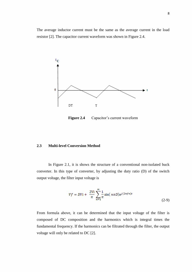
The average inductor current must be the same as the average current in the load
resistor [2]. The capacitor current waveform was shown in Figure 2.4.
Figure 2.4 Capacitor’s current waveform
2.3 Multi-level Conversion Method
In Figure 2.1, it is shows the structure of a conventional non-isolated buck
converter. In this type of converter, by adjusting the duty ratio (D) of the switch
output voltage, the filter input voltage is
(2-9)
From formula above, it can be determined that the input voltage of the filter is
composed of DC composition and the harmonics which is integral times the
fundamental frequency. If the harmonics can be filtrated through the filter, the output
voltage will only be related to DC [2].

9
The output voltage ripple of the DC/DC converter is determined by the
collective effect of the switching frequency, inductance, capacitor, duty ratio and
input voltage, etc. Therefore, the output voltage ripple can be reduced in many ways
such as by improving the frequency of switching, increasing filter inductance or
capacitance, or reducing the output voltage. [2]
However, increasing the switch frequency will increase the switch loss and
reduce the efficiency, and increasing the filter inductance or capacitance will cause
an increase of volume and system cost.
In this project, to reduce the output voltage ripple, a method of reducing the
input voltage is proposed. This new multi-level DC/DC converter structure is
presented in Figure 2.5. It consists of traditional DC/DC converters in series. The
output parts of Buck converters are connected with diode in series which ensures the
output isolation of all converters. In each level the middle diode and switching
element are connected to the negative point of the up buck converter.
Figure 2.5 Proposed multi-level DC/DC converter.
10
As to the conventional multi-level inverter, with the increase of levels and the
number of switch elements, diodes and capacitors have to be added rapidly.
However, the number of switch elements and the number of diodes will be reduced
by N separately in the proposed N-level DC/DC converter. The power loss can be
reduced by minimizing the acting levels according to the level of generating voltage.
2.4 Control scheme
There is several control schemes have been applied in the buck converters
such as sliding-mode control, voltage-mode control and current-mode control. The
external control is required to provide perfect regulation. Without the external
control, the output is dependent on the input voltage and lack of line regulation.
Every control schemes has their own advantages and disadvantages. [3]
The output voltage of DC-DC converter must be a regulated output voltage
under varying load and input voltage condition. The converter component values are
also changing with temperature, pressure, time and so forth. Controlling the output
voltage is needed in a closed loop manner by using voltage feedback. The external
control is required to provide perfect regulation. Without the external control, the
output is dependent on the input voltage and lack of line regulation for every type of
control schemes; they have their own advantages and disadvantages. [4]
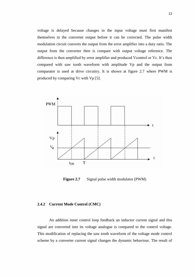
Figure 2.6 below is show the block diagram of feedback control. The
objective of the feedback control is used to ensure the output follow the reference
value and reduce the disturbances to an acceptable level. The feedback network or
control circuitry consists of error amplifier and pulse width modulator (PWM) to
determine the required duty ratio of the power switch to maintain the output at
desired level with fixed value for power converters. There are several forms of PWM
control, but the most popular form is the frequency operation is fixed due to
electromagnetic interference and noise considerations.

11
Figure 2.6 Block diagram for feedback control
2.4.1 Voltage Mode Control (VMC)
The key feature of this control is the existence of a feedback loop which
keeps track of the output voltage variation and adjusts the duty cycle. Furthermore, in
this control scheme, the difference between the output voltage Vc, and a reference
signal, Vref, is processed by a compensation network which generates a control
signal, Vcon. This control signal tells how the duty cycle has to be changed in order to
give the best transient dynamics for the desired output. This control signal is
compared with a periodic ramp signal, Vramp (t), to generate a pulse width modulated
signal which drives the switch [5].
In the voltage mode control scheme, the converter output voltage is sensed
and subtracted from an external reference voltage in an error amplifier. Then the
error amplifier produces a control voltage that is compared to a constant amplitude
saw tooth waveform. After that the comparator produces a PWM signal that is fed to
drives of controllable switches in the dc – dc converter. The duty ratio of the PWM
signal depends on the value of the control voltage. Furthermore the frequency of the
PWM signal is the same as the frequency of the saw tooth waveform. The advantage
of this scheme is simple hardware implementation and flexibility.
The error amplifier reacts in a fast manner to changes in the converter output
voltage. As a result, voltage mode control scheme provides good load regulation
against variations in the load. However regulation against variations in the input
12
voltage is delayed because changes in the input voltage must first manifest
themselves in the converter output before it can be corrected. The pulse width
modulation circuit converts the output from the error amplifier into a duty ratio. The
output from the converter then is compare with output voltage reference. The
difference is then amplified by error amplifier and produced Vcontrol or Vc. It’s then
compared with saw tooth waveform with amplitude Vp and the output from
comparator is used at drive circuitry. It is shown at figure 2.7 where PWM is
produced by comparing Vc with Vp [5].
Figure 2.7 Signal pulse width modulator (PWM)
2.4.2 Current Mode Control (CMC)
An addition inner control loop feedback an inductor current signal and this
signal are converted into its voltage analogue is compared to the control voltage.
This modification of replacing the saw tooth waveform of the voltage mode control
scheme by a converter current signal changes the dynamic behaviour. The result of

13
current mode control is a faster response and mainly applied to boost and buck-boost
converters which suffer from an undesirable non-minimum phase response [6].
With the inductor current taken into account, of course current mode control
performs better, however the application of current mode control to the buck
converter does not gain much benefit over voltage mode control. This is because the
inductor current information can be readily derived from the output voltage in the
case of the buck converter. In addition, with the absence of the low frequency
inductor current dynamics, the inheritances of non-minimum phase problem
associated with the boost and buck-boost converters is automatically eliminated.
High frequency instability in the form of sub harmonics and chaos is possible in
current mode control. Figure 2.8 shows the block diagram for Current Mode Control.
Figure 2.8 Current mode control block diagram
The voltage across the current sense resistor which is represents the actual
inductor current is fed into the current compensator and compared to the desired
current program level. The difference or current error is then amplified and filtered.
After that it is compared with a saw tooth ramp at PWM comparator input to
generate the required duty ratio. This control scheme also provides excellent noise
immunity to the spike sensed in the inductor current. When the clock pulse turns the

14
power switch on, the oscillator ramp (Vco) immediately dives to its lowest level
which means volts away from the corresponding current error level at the input of the
PWM comparator [3].