the design and fabrication of an optical sensor for ... design and fabrication of an optical sensor...
TRANSCRIPT

The Design and Fabrication
The Design and Fabrication
of an Optical Sensor for Monitoring
of an Optical Sensor for Monitoring
the Growth of Mould in Buildings
the Growth of Mould in Buildings
Presented By: Anna Sauer
MEScCandidate in Electrical Engineering
Supervisors: Drs. Sabarinathan, Savory, & Scott

OUTLIN
EOUTLIN
E
•Project Background and Facility
•What is m
ould?
•Existing Technology for use in the
detection of mould
•Design Requirements
•The Full Sensor
•Components of the sensor
•Results
•Im
plementation

THE INSURANCE RESEARCH LAB
THE INSURANCE RESEARCH LAB
FOR BETTER HOMES
FOR BETTER HOMES

THE INSURANCE RESEARCH LAB
THE INSURANCE RESEARCH LAB
FOR BETTER HOMES
FOR BETTER HOMES
Interchangeable
panels to allow
for the testing
of different
finishes, such as
Aluminum
Siding, Brick,
etc.

WHAT IS MOULD?
WHAT IS MOULD?
•Microscopic organisms known as
fungi, includes: m
ushrooms,
yeast, and m
ould
•They play an important role in
nature –
degrading pant and
animal debris
•Reproduce through spores
•Spores can be tracked or blown
indoors on soil particles in the
air

MOTIVATIO
NMOTIVATIO
N
•Mould in buildings is a
major problem for
homeowners and insurance
companies, as it causes
costly property damage and
can pose serious health
risks.
•About 10% of children are
asthmatic and it has been
shown that this is strongly
correlated with indoor
mould growth.

CURRENT W
AYS OF KNOWING IF
CURRENT W
AYS OF KNOWING IF
A BUILDIN
G HAS MOULD
A BUILDIN
G HAS MOULD
•Invasive and Destructive
–Destruction of Property
•Mould Sniffing Dogs
•High Resolution Units
–Georgia Tech
•Electronic Nose
–SCENTAUR, Hamilton Thorne Biosciences,
(http://w
ww.hamiltonthorne.com/reseach/environment/scentaur.htm
)

OUR GOAL
OUR GOAL
•To build and test a sensor
that can m
onitor the
growth of mould spores on
a m
embrane accurately
•40 or so sensors will be
built and installed into the
wall cavity of the control
building

MOULD
MOULD
•There are 4 predominant species of mould that are
found indoors, they are:
–Stachybotrys
–Cladosporium
–Penicillium
–Aspergillus
•Our membranes are from the Cladosporium
Shearosperimum
family
•Two types of membranes:
–PVC (Poly Vinyl Carbon)
–Teflon (Ploy Tetra Fluro
Ethylene (PTFE))
Day 0
Day 2
Day 4
Day 6
Day 8
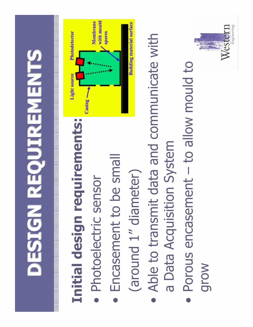
DESIGN REQUIREMENTS
DESIGN REQUIREMENTS
Initial design requirements:
•Photoelectric sensor
•Encasement to be small
(around 1”diameter)
•Able to transm
it data and communicate with
a Data Acquisition System
•Porous encasement –to allow m
ould to
grow

INITIAL EXPERIM
ENTS
INITIAL EXPERIM
ENTS
•Using a Spectrometer to determ
ine the
wavelength that is absorbed by the m
ould.
05
10
15
20
25
30
35
40
410
416
421
427
433
438
444
449
455
460
466
471
477
482
487
493
498
503
509
514
519
525
530
535
541
546
551
556
561
567
572
577
582
587
592
598
603
608
613
618
623
628
Largest reflection shown in Blue Range
450nm

FULL SENSOR
FULL SENSOR

HOUSIN
GHOUSIN
G
Housing units as designed by a 4
thyear group
in Mechanical Engineering, designs done in
Solid W
orks
Battery housing
Micro board
Wireless board
Optical board
Light baffle
Location of
membrane

HOUSIN
GHOUSIN
G
Housing unit as fabricated by the
University Machine Shop

ELECTRONICS
ELECTRONICS
3 Boards –in a tier form
at
1. Optical Board
2. Main Processor Board
3. Data Output Board
With a 4th board for power
Optical
Board
Main Processor
Board
Data Output Board
Main
Power
Inputs/Outputs
Inputs/Outputs
Inputs/Outputs
Inputs/Outputs
Power (6V)
Ground
On/Off Switch to
Boards
Sensor Data
Serial Data
Control of Wireless
Wireless Data

ELECTRONICS
ELECTRONICS
Printed Circuit Boards (PCB)
Designed using Eagle and as fabricated by the
Electronics Shop at UWO
microcontroller
voltage regulator
pins to PC
main power pins
npntransistor
-sw
itch
photodiode
link between
micro &
optical board
LED
Programming pins

DATA ACQUISITIO
N SYSTEM
DATA ACQUISITIO
N SYSTEM
Using
Labviewto
acquire data
through a
serial
connection

RESULTS
RESULTS
This experiment was perform
ed to ensure that the results that are being obtained
from the fabricated PCB are similar to those obtained from the breadboard.
0
0.51
1.52
2.53
3.54
4.55
Da
y 2
Da
y 4
Da
y 6
Da
y 8
Days of Mould Growth
Output Voltage (V)
Fabricated PCB
Breadboard circuit

IMPLEMENTATIO
NIM
PLEMENTATIO
N
•Continue lab testing of the
sensor
•Calibration of the sensor
•Evaluation of current
housing unit
•Fabrication and
implementation of 40
sensors into the control
building