the design and construction of single-stage and …qdg/publications/internalreports/baglo-04.pdf ·...
TRANSCRIPT

Co-op Work Term Report
Summer 2004:
The Design and Construction ofSingle-Stage and Dual-Stage
Photodetectors
by Jordan Baglo
Submitted September 7, 2004.
SN: 39481023
PHYS 298
Employer: Dr. Kirk Madison

The Design and Construction of
Single-Stage and Dual-Stage
Photodetectors
Jordan Baglo
SN: 39481023
September 7, 2004

I Preface
This report is a very broad overview of the design, construction, and testing oftwo different models of photodetectors which I carried out during the monthsof May through to September, in my Co-op work term placement in the lab-oratory of Dr. Kirk Madison of the UBC Department of Physics. During mywork term I was also assigned other individual projects, including the designand construction of the power supply boxes that will be used as the primarypower source for much of the laboratory equipment being built (including thesephotodetectors). I also made contributions to many other laboratory projects,such as a voltage regulator circuit and a diode laser protection circuit, withwhich I had various degrees of involvement. However, I spent the majority ofmy time and effort throughout the term working on the photodetectors, and Ihave decided to write my work term report on the single-stage and dual-stagephotodetectors for this reason.
In this report, I will briefly discuss the field of research and type of exper-iment being conducted in the lab, placing the photodetectors in this context.After the introductory content, I will describe the initial evaluation of the opera-tional amplifier used in the photodetector circuit, as well as the radio-frequency(RF) design problems—and solutions—that were encountered. Next follows adetailed description of the construction of the original single-stage photodetec-tor, and the methods that I used to evaluate the photodetector’s performance.Finally, the issues involved in the design and construction of the dual-stage pho-todetector are discussed, and the development process for the two-stage detectoris outlined.
I must stress that, although the coverage of this report ends with its finalsubmission, the photodetectors are still very much works in progress. Not onlydo the detectors need to be “mass produced,” in quantities beyond the sin-gle prototypes being considered for this project, but many modifications andimprovements to the designs of the the detectors are pending as well. The de-signs of the photodetectors (particularly the dual-stage model) are continuouslyevolving, and may continue to change with the requirements placed on them bythe experiment.
For their contributions to both the photodetector project and this report, Iwould like to thank the members of my lab—Dr. Madison, Dr. Bruce Klappauf,Janelle van Dongen, Amy Liu, and Tao Kong. I am especially grateful to Dr.Madison for providing me with the opportunity to work on this project, as wellas for his guidance with the design of the circuits, and his thorough explanationsof the “big picture” of the experiment. Dr. Klappauf provided me with muchassistance with testing my circuits, especially with troubleshooting my early opamp stability problems. Janelle, Amy, and Tao were always ready and willingto help me with my circuit construction, to suggest ideas for this report, or justto provide moral support. My project has been made much less difficult—andmuch more enjoyable—with the assistance of all my group members, and it isto them I owe thanks for my great experience this summer.
ii

Contents
I Preface . . . . . . . . . . . . . . . . . . . . . . . . . . . . . . . . ii1 Introduction . . . . . . . . . . . . . . . . . . . . . . . . . . . . . . 1
1.1 The Research . . . . . . . . . . . . . . . . . . . . . . . . . 11.2 The Detectors . . . . . . . . . . . . . . . . . . . . . . . . . 2
2 The Single Stage Photodetector . . . . . . . . . . . . . . . . . . . 32.1 Initial Design . . . . . . . . . . . . . . . . . . . . . . . . . 32.2 Preliminary Evaluation of the OPA686 Op Amp . . . . . 42.3 Building the Single-Stage Photodetector . . . . . . . . . . 72.4 Measuring the Frequency Response . . . . . . . . . . . . . 82.5 Conclusion . . . . . . . . . . . . . . . . . . . . . . . . . . 12
3 The Dual-Stage Photodetector . . . . . . . . . . . . . . . . . . . 133.1 Introduction . . . . . . . . . . . . . . . . . . . . . . . . . 133.2 The Circuit Design . . . . . . . . . . . . . . . . . . . . . . 133.3 The Board Layout . . . . . . . . . . . . . . . . . . . . . . 163.4 Building the Dual-Stage Photodetector . . . . . . . . . . 173.5 Conclusion . . . . . . . . . . . . . . . . . . . . . . . . . . 18
Appendices . . . . . . . . . . . . . . . . . . . . . . . . . . . . . . . . . 19A The Operational Amplifier . . . . . . . . . . . . . . . . . . . . . . 20
A.1 Basic Uses and Properties . . . . . . . . . . . . . . . . . . 20A.2 Negative Feedback and the “Golden Rules” . . . . . . . . 20A.3 The Inverting Amplifier . . . . . . . . . . . . . . . . . . . 21A.4 The Noninverting Amplifier . . . . . . . . . . . . . . . . . 22
B The Laser Lock System . . . . . . . . . . . . . . . . . . . . . . . 23B.1 Doppler-free Saturated Absorption Spectroscopy . . . . . 23B.2 Phase Sensitive Detection . . . . . . . . . . . . . . . . . . 23
C The Photodetector Enclosure . . . . . . . . . . . . . . . . . . . . 25D List of Equipment . . . . . . . . . . . . . . . . . . . . . . . . . . 29
D.1 Design and Data Analysis Software . . . . . . . . . . . . . 29D.2 Electrical/Optical Measurement Equipment . . . . . . . . 29D.3 Laser Equipment . . . . . . . . . . . . . . . . . . . . . . . 29D.4 Power Supplies and Signal Sources . . . . . . . . . . . . . 30D.5 Soldering and Assembly Equipment . . . . . . . . . . . . 30D.6 PCB Processing Equipment and Supplies . . . . . . . . . 30
E List of Vendors . . . . . . . . . . . . . . . . . . . . . . . . . . . . 31Bibliography . . . . . . . . . . . . . . . . . . . . . . . . . . . . . . . . 32
iii

List of Figures
1 Velocity distribution of the first BEC . . . . . . . . . . . . . . . . 12 The original photodetector design. . . . . . . . . . . . . . . . . . 43 The OPA686 on a “Surfboard” surface mount adaptor. . . . . . . 54 An assembled photodiode amplifier. . . . . . . . . . . . . . . . . 85 The original frequency response data with the LED . . . . . . . . 96 Several LED-measured frequency responses. . . . . . . . . . . . . 107 A comparison with a Thorlabs detector. . . . . . . . . . . . . . . 118 The dual-stage photodetector schematic. . . . . . . . . . . . . . . 159 Both sides of the circuit board trace. . . . . . . . . . . . . . . . . 1610 A fully assembled dual-stage photodetector board. . . . . . . . . 1711 The inverting and noninverting amplifiers . . . . . . . . . . . . . 2112 Photodetector enclosure design, overview . . . . . . . . . . . . . 2513 Photodetector enclosure design, front panel . . . . . . . . . . . . 2614 Photodetector enclosure design, bottom plate . . . . . . . . . . . 2715 Photodetector enclosure design, top plate . . . . . . . . . . . . . 2716 Photodetector enclosure design, rear plate . . . . . . . . . . . . . 2817 Photodetector enclosure design, side panels . . . . . . . . . . . . 28
iv

List of Tables
1 Electronics, CAD, and analysis software used. . . . . . . . . . . . 292 Measurement equipment used. . . . . . . . . . . . . . . . . . . . . 293 Laser equipment used for testing. . . . . . . . . . . . . . . . . . . 294 Power supplies and signal sources used. . . . . . . . . . . . . . . 305 Soldering and assembly equipment. . . . . . . . . . . . . . . . . . 306 PCB processing chemicals and equipment. . . . . . . . . . . . . . 307 A list of vendors, distributors, and other businesses used . . . . . 31
v

1 Introduction
1.1 The Research
This project takes place in the laboratory of Dr. Kirk Madison, of the Depart-ment of Physics at the University of British Columbia. The focus of the group’sresearch, which falls both in the fields of atomic, molecular, and optical (AMO)physics and in condensed matter physics, is that of Quantum Degenerate Gases.
1.1.1 Bose-Einstein Condensation
In short, the study of Quantum Degenerate Gases involves the production ofultra-cold atomic gases, and the highly non-classical phenomena which occurin systems of such gases. The most well-known example of such a system isthe Bose-Einstein Condensate (BEC). Although Bose-Einstein condensation waspredicted by Albert Einstein1 in 1924, the phenomenon was not observed untilJune 1995, when Eric Cornell and Carl Weiman created the first BEC at JILA(at the University of Colorado, Boulder) in a gas of 87Rb atoms (see Figure 1).
Figure 1: A computer-generated image of the velocity distribution of the firstobserved Bose-Einstein condensate at JILA. This image is from the JILA web-site, at http://jilawww.colorado.edu/bec.
The phenomenon of Bose-Einstein condensation occurs when bosonic atoms
1Einstein’s work was based on the noninteracting particle statistics ideas of SatyendraBose, which are now known as Bose-Einstein statistics; Bose himself played no direct role inEinstein’s prediction of the BEC [1].

(those with integer spin) are cooled sufficiently low, typically on the order ofhundreds of nanokelvin2, such that the density of atoms with a given energynear the ground state becomes extremely high. When cooled below some criticaltemperature Tc, some atoms coalesce into the ground state, with all of the atomscondensing together into the ground state in the limit as T → 0 [1].
What is remarkable about this condition is that the ground-state rubidiumatoms—which being bosons, are not subject to the Pauli exclusion principle—have the exact same quantum state; they become a single, massive particle de-scribed by a single wavefunction! Such Bose-Einstein condensates can be madeto have more than 106 atoms, and can have lifetimes in the tens of seconds [13].These macroscopic3 quantum systems provide an unprecedented opportunity todirectly manipulate and observe quantum phenomena in the laboratory, provid-ing a veritable scientific “playground” for the experimentation with quantumand condensed matter systems that had been inaccessible for decades. Theconstruction of a rubidium BEC is among the first goals of this group.
1.1.2 Degenerate Fermi Gases
Although such condensates of bosonic atoms provide excellent experimentalopportunities for the study of many quantum phenomena, the study of ultra-coldfermions is also of much interest. Due to the Pauli exclusion principle, no morethan one fermion can occupy the same quantum state (when opposite spins areconsidered to be different states), and thus no exact fermionic equivalent of theBose-Einstein condensate can be obtained. However, ultra-cold gases of fermionsexhibit their own degenerate, highly-correlated behaviours (such as Cooper pairformation) [10]. The study of such such behaviours in degenerate Fermi gaseswill prove invaluable for testing condensed matter theories—particularly thosepertaining to high TC superconductivity—which involve systems of fermionssuch as electrons.
One method of obtaining such ultra-cold systems of fermions is to use aFermi-Bose mixture, a mixture of fermions and bosons. By first creating aBEC with the bosons in the mixture in the same manner as usual, the fermionsare cooled by the BEC, beyond what is typically possible with other techniquesusing fermions alone [10]. This method of sympathetic cooling will be applied inthis lab—using 87Rb as the bosonic species and 6Li as the fermionic species—tocreate and study such systems of degenerate Fermi gases.
1.2 The Detectors
1.2.1 General Applications
The photodetectors were not designed for (nor shall they be dedicated to) asingle application in the laboratory; rather, they were designed to be used inmany different situations in which light needs to be measured or monitored.
2Using laser cooling and magneto-optical traps; see [12], for example3Macroscopic, that is, for a quantum system!
2

The countless possible uses of the detectors will require of them the ability tomeasure light signals with a wide range of characteristics, from weak to intense,and from steady to high-frequency; this needed versatility places constraints onthe design of such a general-purpose photodetector.
One of the most common—and least technically demanding—uses of thephotodetectors will be the monitoring of the light intensity of the direct4 laserbeams. The detectors will also be used to measure the fluorescence of thetrapped atoms, as well as that of the cold atom beams. The photodetectors mayadditionally be used as part of a Fabry-Perot interferometer, used to monitorthe wavelength of the beams.
1.2.2 The Laser Locking System
Although the detectors will not be used for just a single purpose, there is oneapplication which stands out as among the most important: the laser lockingsystem. This locking system uses the techniques of Doppler-free saturated ab-sorption spectroscopy and phase-sensitive detection to provide the necessaryfeedback loop to lock the laser wavelengths to the desired atomic line. For abrief discussion of these techniques, see Appendix B.
In terms of the requirements the locking system places on the photodetectors,since the piezoelectric element will modulate the AOM at roughly 100 kHz, it willbe necessary for the photodetectors to have frequency responses well above thisrange. Additionally, since the changes in light intensity on the photodetectorsdue to absorption of the beam will be small, high-frequency modulations ridingon large offsets, it would be useful to produce a detector that only amplifiesthis modulation. These issues have been dealt with in the construction of thephotodetectors, which is the subject of this report.
2 The Single Stage Photodetector
2.1 Initial Design
The original plan for the photodetector was based on a design by Todd Meyrathof the University of Texas at Austin [8]. This basic design (see Figure 2) utilizesa high-speed photodiode together with a high speed operational amplifier, withthe aim of producing a high-speed photodetector unit.
The operational amplifier that was chosen was the Burr-Brown OPA686.This op amp has an extremely high gain-bandwidth product 5 of 1600 MHz;for comparison, typical general-use op amps have bandwidths in the tens ofmegahertz and under. Although the high bandwidth will allow the detection of
4The “direct” beams may have first been been split, filtered, polarized, or otherwise atten-uated; for sufficiently intense beams, neutral density filters will be necessary to prevent thebeam from saturating the photodiode and the output of the operational amplifier, in order tokeep the measurements in the linear regime of the photodetector.
5Commonly known as the unity-gain bandwidth, fT , which is the bandwidth at a gainfactor of one; for op amps that are not stable at a gain of one, this value is interpolated.
3

PHOTODIODE AMPLIFIER
-
+
Todd Meyrath Oct 2003
Based on the sample design from the OPA686 datasheet
OPA686
+
10µF tantalum
0.1µF 1206 chip
+
Power Supply Bypass
10µF tantalum
0.1µF 1206 chip
0.1 to 10µF chip or tant. capacitor
or film capacitor for high voltages
-
+
OPA686
0.1µF 1206 chip
100pF
1206 chip
Rfeedback
1206 chip
-V
50Ω 1206 chip
BNC
output
Rfeedback
1206 chip
+5V
-5V
3
2
6
4
7
Fer
rite
Fer
rite
Ferrite
Cfeedback
1206 chip
Photodiode Reverse Bias
Photodiode
Figure 2: The original photodetector design, by Todd Meyrath [8].
a greater range of signals, thus producing a more versatile detector, the op ampwill also be more vulnerable to noise and self-induced oscillations than sloweroperational amplifiers. These problems were encountered—and dealt with—during the course of the project, and are discussed in the report below.
The operational amplifier will be used in a transimpedance configuration,which is essentially an current-to-voltage converter. The feedback resistor fromthe op amp’s output to its inverting input sets the “transimpedance gain”.Whatever current is input into the transimpedance amplifier will be producean output voltage according to Ohm’s law, helped along by the output of theop amp; that is, Vout = IinRf , where Rf is the transimpedance gain. Thisenables components like the photodiode, which are unable to produce the nec-essary large voltages to “enforce” their current output across heavy loads, toproduce voltages large enough for easy observation with an oscilloscope6. Thisis essentially the nature of the photodetector circuit to be built.
2.2 Preliminary Evaluation of the OPA686 OperationalAmplifier
Before designing the full photodetector, it was decided that a test of the perfor-mance and characteristics of the workhorse of the photodiode amplifier circuit,the Burr-Brown OPA686 operational amplifier, would provide useful insight forthe detector design. A simple test circuit which used the op amp in an inverting
6More details about op amps may be found in Appendix A, and in [6]
4

amplifier configuration7 was to be set up for this purpose. The power supplyconnection—complete with decoupling capacitors—was set up the same as inthe intended final design (see Figure 2, on the right), and the gain was set tobe 20 through the use of a 1 kΩ feedback resistor and a 50 Ω input resistor (seeSection A.3).
2.2.1 Early Breadboard Testing
The first attempt at construction of this test circuit was performed on a bread-board. The OPA686 (and most of the other components that will be used inthis project) is a surface mount component; in particular, it has an SOIC-8 8
package. Such components are typically very small, and have no “through-hole”leads for which holes must be drilled in a board; rather, these components areelectrically connected to the board by soldering tiny contacts or leads to pads onthe board. The only way to test such components on a breadboard is to solderthem to an adaptor board (a “Surfboard,” see Figure 3) with pads designed foran SOIC-8 footprint connected to corresponding SIP pins (“Single Inline Pins,”with 0.1” pitch) that fit into common breadboards.
Figure 3: The minuscule OPA686 on a “Surfboard” surface mount adaptor.Note the size comparison with the penny!
In early testing, the Surfboard on which the OPA686 was soldered wasplugged into a breadboard, on which all of the inputs, outputs, power sup-ply connections (with ferrite filters and decoupling capacitors) and feedbackcomponents were arranged, using standard through-hole components. Whenthis inverting amplifier test setup was evaluated by using a sinusoidal signalfrom a function generator, the results were found to be extremely unsatisfac-tory; the amplifier (with few exceptions) did not work. Most of the time, theoutput signal consisted of wild, full-scale oscillations which appeared essentiallyuncorrelated with the input signal, and seemed to be the result of some sort ofself-resonance property of the op amp itself.
7The inverting amplifier was chosen for testing purposes because it matches most closelythe transimpedance amplifier configuration to be used; the inverting amplifier is essentially atransimpedance amplifier with an input resistor converting input voltage into current.
8This is an abbreviation of “8-pin Small Outline Integrated Circuit”
5

Occasionally it was found, for particular (inexplicable) values of the positiveand negative power supply voltages, and particular values of the amplitude andDC offset of the function generator, that an output signal which was a distortedbut recognizable version of the input sine wave could be observed. Such outputsignals were always lower in amplitude than the input signal itself. Moreover,the particular combinations of voltages which produced such signals were seldomreproducible.
Based on suggestions from others in the group, the UBC Physics ElectronicsLab, and the op amp’s datasheet [2], it was decided that RF (radio-frequency)design techniques would need to be taken into consideration.9 Of most concernwere the lengths of the connections on and to the breadboard from the op amp.However, simply moving the breadboard components closer and shortening thewires had little effect.
It was suggested that the breadboard power supply might be responsible forthe oscillations, and that an oscilloscope check of the power supply with theamplifier circuit in operation would be informative. Indeed, it was discoveredthat, when comparing the output of the op amp with the power supply voltages,there were large oscillations of the power supply voltage that were correlatedwith the amplifier output. However, correlation does not (necessarily) implycausation, and it was never determined conclusively whether the power supplycaused the amplifier to oscillate, or vice versa, or whether the two acted togetherin producing the oscillations.
2.2.2 RF Design Modifications
In order to eliminate any effects due to poor RF design, a new op amp circuitwas set up on another Surfboard, only this time, the power supply ferrites anddecoupling capacitors were soldered directly to the Surfboard, as close to theop amp as possible. The purpose of the ferrites in series with the power lines isto block (or at least attenuate) any RF pickup from the power supply lines; thedecoupling capacitors between the power lines and ground provide additionalpower supply noise rejection by shunting high-frequency power spikes to ground,and “filling in” high-frequency power dips. By placing the supply filtering closeto the op amp, the length of wire between the filters and the op amp over whichparasitic RF signals can be accumulated is decreased dramatically.
Additionally, a thin copper sheet was superglued to the back of the bread-board, which was to act as a ground plane. All of the ground connections on theboard were soldered to this ground plane, which was in turn connected to theground of the breadboard power supply. This is a common RF design techniquewhich is intended to shield the circuit from noise, as well as to reduce the effectsof ground loops.10 By making short connections to a large conductor acting asa common ground, such ground loop problems are kept to a minimum.
9Some good RF design references include the books by DeMaw [3] and Everard [5].10Ground loops occur where wires connecting components in (or between) circuits to a
common ground are long enough to act as large antennae, which are prone to receiving RFpickup. See [9] for a good reference.
6

The new circuit was assembled on the breadboard, on which the input andfeedback resistors still remained, since it was found to be topologically impossi-ble to connect a surface mount resistor across the op amp, using the traceson the Surfboard. When this circuit was tested, the output was improvedimmeasurably—the output signal always followed the input signal, with nopower supply tweaking necessary—yet the output was still quite noisy, andthe gain was incorrect (as the output signal amplitude was smaller than that ofthe input signal).
This situation was finally rectified when the input and feedback resistors(through-hole, not surface mount) were soldered directly to the Surfboard, withthe feedback resistor’s leads allowing it to connect above and across the op amp.With the feedback components closer to the op amp, and with no remaining un-filtered connections to the breadboard, the circuit finally worked properly, withthe proper voltage gain of -20, and with significantly reduced noise. Furthertesting showed no problems, with the exception of some instability at low fre-quencies (below 1 kHz), which was determined to be an issue with the functiongenerator and not the amplifier.
2.3 Building the Single-Stage Photodetector
After satisfactorily testing the OPA686 operational amplifier in an invertingamplifier configuration, a complete prototype of the photodetector unit wasready to be built. Assembly of the circuit was to involve more than just solderingthe components to the printed circuit board (PCB); the boards themselves wereto be processed in the lab as well.
Although there are other methods of making PCB’s, the most accessiblemethod for “homemade” board making involves a light exposure method, similarto development methods used in photography. The boards to be processedhave a layer of copper on each side of the board, covered in a light-sensitivechemical resist layer. When an area of the board is exposed to ultravioletlight (a fluorescent light works well), the chemical resist becomes vulnerable tothe developer chemical (in this case, NaOH), and immersing the board in thedeveloper removes the exposed resist. Finally, exposing the board to a chemicaletchant (this lab uses ammonium persulphate) removes all copper that is nolonger protected by the resist.
After rinsing the board in water to remove the caustic (and poisonous)etchant, the development process is complete, with copper wires remainingwhere the board was not exposed to light. Thus by placing a standard laser-printed transparency over a board as a mask while exposing the board, the cop-per “trace” of a circuit may be transferred to a board. For two-sided boards,both sides of the board are exposed before developing. The only added diffi-culty in processing two-sided circuit boards is the need to align both sides ofthe board exactly opposite each other, which can sometimes be a difficult task.
For this photodiode amplifier circuit, a single-layer board transparency mask,containing 16 circuits, had already been created by the designer [8], thus therewas no need to design a new mask. The first test board to be processed was
7

Figure 4: An assembled photodiode amplifier.
slightly overdeveloped; a second try produced a board that was good enoughfor assembly. Using a drill press, holes for the power supply wires and the BNCleads and supports were drilled, and then segment of the board was cut off fromthe rest, upon which a circuit was assembled.
The circuit was built in accordance with the original design (see Figure 2),using a Hamamatsu S5973 photodiode and a feedback resistance of 10 kΩ, butwith no feedback capacitor to begin with. Except for the photodiode and theboard-mounted BNC, most of the components were in surface mount packages.For the resistors, capacitors, and ferrites, this required no special solderingtechniques 11 other than the use of tweezers to hold the component in placeduring soldering. For the op amp’s eight small pins, two pins at opposite cornerswere soldered first, after which the rest of the pins were easily soldered; however,the pins were often found to make poor contact with the copper pads of the PCB,and a hot air rework station was used to force the solder to “flow” up the pinsfrom the pads.
After the photodiode amplifier circuit had been assembled (see Figure 4),it was mounted on a metal post and connected to a power supply (and to theoscilloscope), and a brief, qualitative test of the photodetector was performed.An LED in series with a current-limiting resistor was connected to a functiongenerator; by placing the modulated LED in front of a photodiode, a clean,low-noise signal was observed from the detector, whose response appeared to bequite linear.
2.4 Measuring the Frequency Response
2.4.1 Initial Attempts with an LED
One of the most important steps in the construction of the detector was anevaluation of its frequency response. Although preliminary calculations using
11For an excellent online guide to surface mount soldering, see [4].
8

1 10 100 1000 10000 100000 1000000Frequency (Hz)
30
35
40
45
50
Amplitude (mV)
Figure 5: The original 10 kΩ frequency response data taken with the LED.
formulae in [8] and [2] predicted a bandwidth12 on the order of 80 MHz, theparasitic capacitances and resistances of the circuit could not be determinedvery accurately. To rule out a bandwidth that was orders of magnitude below(or above) predictions, a measure of the actual bandwidth was desired.
For the frequency measurements, a more permanent LED signal tester wasbuilt, by drilling holes in a bent aluminum sheet, in which were mounted a BNCand a red LED. A 50 Ω current-limiting resistor was connected between the BNCsignal wire and the anode of the LED, with the cathode connected through awire to the BNC ground. This was initially modulated with the only available3 MHz function generator, despite being incapable of reaching the predictedbandwidth.
Surprisingly, a drop-off in amplitude was observed even in the low (2–3)MHz range (see Figure 5). Since the function generator that was used only hada range of 3 MHz, it was deemed most likely to be a problem with the functiongenerator in its highest range. A different function generator with a range of20 MHz13 was obtained for further testing, so as to rule out this possibility.
Three frequency response data sets were taken with the new function genera-tor: one for the original 10 kΩ feedback resistor, and one each after the feedbackresistor had been replaced with values of 20 kΩ and 5 kΩ. While the bandwidthof the detector is supposed to decrease by a factor of 1
√
2for each doubling of
the feedback resistance Rf , the bandwidths stayed roughly the same—around3 MHz—for all values of the feedback resistance (see Figure 6). This stronglysuggested—since the function generator had been tested—that the LED itselfhas a bandwidth of 3 MHz; a quick measurement of the LED’s frequency re-sponse using a fast commercial detector (the Thorlabs PDA155) confirmed thisfact.
2.4.2 Testing with a Laser Diode
In order to provide an accurate measurement (or even an estimate) of the band-width and frequency response of the detector, a different modulated light source
12Here, the bandwidth is defined as f−3dB, which is the frequency at which the outputamplitude drops to 1
√
2, or -3 dB, below the maximum.
13Although it was marked as 20 MHz, it worked up to almost 25 MHz.
9

1 10 100 1000 10000 100000 1000000 10000000Frequency (Hz)
30
40
50
60
70
80
90
100
Amplifier Output Percent of Maximum
Photodetector Frequency Response:Blue = 5k, Red = 10k, Green = 20k
Figure 6: Frequency response data taken with the LED: Points are blue forRf = 5 kΩ, red for Rf = 10 kΩ, and green for Rf = 20 kΩ.
would need to be obtained. For this purpose, a 5 mW laser diode was used,intially connected through current-limiting resistors directly to the faster func-tion generator. The function generator was set up with a small amplitude ridingon a large DC offset, such that the light modulation was always in the linearregime of the laser’s “Intensity vs. Voltage” function.
Since the Thorlabs PDA155 photodetector had a known bandwidth of 50 MHz,it was used to test the combined frequency response of the laser diode and func-tion generator. The output of the function generator was also monitored on theoscilloscope, using a 1 MΩ input impedance so as to minimally perturb the sig-nal through measurement. When the Thorlabs detector’s output was observedat different modulation frequencies, the amplitude started to decline around14 MHz; however, the output amplitude of the function generator also showedthis same decline. When the Thorlabs detector was replaced with the lab-builtdetector, the same response was observed. No “rolloff” was observed in eithercase that could not be attributed to the laser diode-function generator circuit,suggesting that the bandwidths of both detectors were somewhat higher than25 MHz. The bandwidths of the detectors were too high to be measured withthe available equipment.
2.4.3 Comparison with a Commercial Detector
Since the bandwidth of the photodetector was known to be at least 25 MHz, andknowing that the intended uses of the photodetector would seldom require abandwidth greater than several megahertz, the bandwidth of the photodetectorwas declared to be more than sufficient. However, while an exact measurementof the bandwidth of the detector was deemed unnecessary, it was decided that aside-by-side comparison of the performance of the lab-built detector with thatof the Thorlabs detector would be informative.
In order to compare the performance of the two detectors with the same
10

signal, a glass microscope slide was positioned with a large angle of incidence inthe beam, acting as a simple beam-splitter. The angle was adjusted to roughlyequalize the split beam intensities. The Thorlabs detector was placed in thereflected beam, while the transmitted beam was reflected off two mirrors towardsthe other detector.
To drive the laser diode, a new technique was used; the function generatorstill provided the DC offset, but the modulation was provided by a recentlyobtained Agilent 8648A RF Synthesizer, which could modulate up to 1 GHz.Both sources were connected to the laser diode via an improvised circuit board,on which the RF synthesizer was connected through a 50 Ω resistor and 1 nFcapacitor to protect it from the DC offset, and the function generator wasconnected through ferrite beads to protect it from the modulation.
The idea behind testing the two detectors simultaneously was to negate thefrequency dependency of the laser’s modulation amplitude. Where the responsesof the detectors are linear, both will observe the same proportional variations ofthe light modulation, and the ratio of the detector outputs will remain constant.Assuming the detectors have different bandwidths, the ratio of the detectors’output amplitudes will change when one detector’s output begins to drop fasterthan the other; a second change will be observed where the faster detector’sreponse declines as well. This gives some indication of the bandwidths of thedetectors.
0 20 40 60 80 100Modulation Frequency (MHz)
0
0.2
0.4
0.6
0.8
1
1.2
Thorlabs/QDG Ratio
Frequency Response Ratio at 10 kOhms
0 20 40 60 80 100Modulation Frequency (MHz)
1
1.5
2
2.5
3
3.5
4
4.5
Thorlabs/QDG Ratio
Frequency Response Ratio at 10 kOhms
0 20 40 60 80 100Modulation Frequency (MHz)
0
100
200
300
400
500
600
Amplitude (mV)
Frequency Response Comparison at 10 kOhms
0 20 40 60 80 100Modulation Frequency (MHz)
0
100
200
300
400
500
600
Amplitude (mV)
Frequency Response Comparison at 50 kOhms
Figure 7: The results of the comparison with the Thorlabs detector. Rf = 10 kΩon the left and 50 kΩ on the right; the lab detector amplitudes are in red, Thorlabamplitudes are in blue, and ratios are in green.
When the measurements were taken with a feedback resistance of 10 kΩ,the lab-built detector clearly outperformed the Thorlabs detector (see Figure7, left); it reached its peak near 40 MHz, 10 MHz after the Thorlabs detector,and while the Thorlabs detector’s amplitude drops to near zero by 100 MHz,the lab-built detector maintains an amplitude above 50 mV out to 250 MHz!
For a feedback resistance in the lab-built detector of 50 kΩ, the situation is
11

reversed (see Figure 7, right); the Thorlabs detector significantly outperformsthe lab-built detector14. The behaviour is as expected, since the increase infeedback resistance by a factor of 5 should scale the frequency response by 1
√
5;
the increase in the amplitude ratio near 20 MHz corresponds to the “rolloff” ofthe lab-built detector, roughly 1
√
5lower than its 45 MHz rolloff with Rf = 10 kΩ.
Having tested the frequency performance of the photodetector for both feed-back values, it was decided that the 10 kΩ feedback resistance provides the bestcompromise between gain and bandwidth. This will be the value chosen forfuture photodetector units to be assembled.
2.5 Conclusion
The initial goal of constructing and testing a general-purpose photodetectorappropriate for most laboratory uses appears to have been met. The small sizeof the circuit (with 16 circuits fitting on a board) will allow the photodetectorsto be placed whatever tight spaces may be necessary. Additionally, the veryhigh bandwidth (around 45 MHz for Rf = 10 kΩ) is orders of magnitude greaterthan what will be required for most situations, and should be sufficient for anyhigh-frequency monitoring applications which may arise. With the exception ofthe design of a metal enclosure to protect and mount the circuit, only the “massproduction” phase of the single-stage photodetector project remains.
14Note that a neutral density filter was used to attenuate the beam for the 50 kΩ lab-builtdetector; however, this only scales the ratio by a constant factor.
12

3 The Dual-Stage Photodetector
3.1 Introduction
During the construction, testing, and evaluation of the original detector design,it was decided that a separate photodetector model should be built for the satu-rated absorption monitors, to be used in the laser locking system (see AppendixB). The signals which the locking system photodetectors will be monitoring willbe small modulations of around 100 kHz, on top of a steady light intensity, withthe modulation typically being only 1% of the steady intensity. Such a signalis ill-suited for use in the locking system, which really only “cares about” themodulation.
A better detector for this purpose would only amplify the modulation for itsoutput. The simplest way to achieve this is to use two amplification stages: thefirst to amplify the DC signal to usable levels for DC filtering, and a second toamplify only the remaining modulation. This is the basic design of the dual-stage photodetector that was constructed in this report.
In addition to the photodetector circuit itself, a metal enclosure for thedetector was designed and submitted to the UBC Physics Machine Shop to bemachined. This will not be covered in the body of the report below, but anoverview of the enclosure may be found in Appendix C.
3.2 The Circuit Design
The design of the dual-stage photodetector was based on a combination of twoseparate designs: the original single-stage design [8], and a dual-stage photode-tector designed by the JILA Electronics Lab [7]. The DC stage of the detectorwas to be the same as the original one-stage design. The AC stage, however,would consist of a high-pass RC filter15 after the output of the DC stage, con-nected into the input of a non-inverting amplifier (see Appendix A.4).
The operational amplifier that was chosen for the AC stage was the AnalogDevices AD829, which has a gain-bandwidth product of 750 MHz. Incidentally,between the time that the OPA686 was ordered for the original detectors andthe ordering of parts for the new detectors, the OPA686 was to declared by Burr-Brown to be nearing obsolescence, and was no longer recommended for new use.Fortunately, there was a recommended replacement op amp, the Burr-BrownOPA846, that was almost exactly equivalent, but with a higher gain-bandwidthproduct of 1750 MHz; this was the op amp that was chosen for the DC stageof the dual-stage detectors, as well as for future production of the single-stagedetectors.
One feature that was to be built into the new detectors was the ability toswitch the output between the AC and DC stages; that is, the ability to “turnoff” the AC amplification stage, and divert the output of the DC stage directly tothe BNC (but through a 50 Ω output resistor for impedance matching, as before).
15An RC high-pass filter consists of a capacitor in series with the line, and a resistor toground. Such a filter blocks low frequencies, with a rolloff at f−3dB = 1
2πRC.
13

This would not only allow the absolute DC intensity of the saturated absorptionpump and probe beams to be checked, it would also allow the detectors to beused for general purpose light detection when necessary. To implement this, theoutput of the DC stage would need to be switched between the AC stage inputand the BNC, and the AC stage output would also need to be simultaneouslyswitched between the BNC and somewhere else. If the AC stage output isnot disconnected from the DC stage while its inputs are disconnected, it mayintroduce its own noise, offsets, or oscillations to the DC output, which would beundesirable. In order to switch both connections, a double-pole double-throw16
was necessary.Another feature which was desired was the ability to adjust the value of
the gain for the AC stage. This would be made possible through the use of apotentiometer as part of the feedback resistance of that stage. Another resistorin series with the potentiometer would be necessary to maintain a minimumgain of 20, since the AD829 was identified in its datasheet as being unstablefor gains smaller than this value. The AC stage was designed to use a 20 kΩpotentiometer in series with a 3.8 kΩ resistor for the feedback loop, and a 200 Ωresistor to ground. Using Equation 7 derived in Appendix A.3, the minimumgain is:
Gmin = 1 +Rf,min
Rg
= 1 +3.8 kΩ
200 Ω= 1 + 19 = 20 (1)
And the maximum gain is:
Gmax = 1 +Rf,max
Rg
= 1 +23.8 kΩ
200 Ω= 1 + 119 = 120 (2)
A 20 kΩ “offset trim” adjustment potentiometer was also included for theAD829, to make use of its offset adjustment pins. This potentiometer takesa −15 V supply input to its center pin, with the two outside pins connectedto the offset adjustment pins of the AD829. This configuration “splits” the−15 V supply between the two pins, with one pin receiving xVolts and theother receiving 15 − xVolts. The offset trim control is optional, and in futureconstruction of the dual-stage photodetector, it may be omitted, but in case itis found to be necessary, the option to include it should be built into the board.
Finally, for the DC stage, a constant feedback resistance (and transimpedancegain) of 50 kΩ was chosen. Although this results in a smaller bandwidth thanif a 10 kΩ resistor was used, this bandwidth is still around 20 MHz, which is atleast two orders of magnitude greater than the approximately 100 kHz modula-tion the detectors were designed to observe. The sacrificed bandwidth will resultin a gain (and thus a signal) which is five times larger, which may sometimesrequire optical attenuation to avoid saturating the DC amplification stage. Thisoccasional need for attenuation does not outweigh the benefit of being able toobserve signals which are five times weaker, as it is usually much harder toincrease a weak signal strength than to attenuate a strong one.
16Or “DPDT”: essentially, a switch controlling two separate lines (poles), with two possibleconnections (throws) for each line.
14

Figure 8: The dual-stage photodetector schematic.
15

The schematic for the complete circuit design, combining all of these designspecifications, is shown in Figure 8.
3.3 The Board Layout
In order to construct this circuit, a circuit board would need to be laid out,according to the design. The main program that was used to design the circuitboard (and draw the schematic) for the dual-stage photodetector was EAGLE,an electronics design suite produced by CadSoft.
Before designing the board, there were several decision to make regarding thephysical composition of the circuit. The most important decision was whetherto use surface mount or through-hole components on the board. In some cases,there was little choice; the OPA846 is only available in surface mount form, andthe BNC, the photodiode, and the wires from the board to the panel mount DINpower connector would require through-holes to be drilled. For the remainderof the components, there was a choice between the two package types whichneeded to be resolved.
Figure 9: Both sides of the printed circuit board copper trace for the dual-stagephotodetector. The top side is on the left.
In the interest of building a compact board that would be more convenientfor laboratory use, all of the capacitors and fixed-value resistors on the board—which comprise the bulk of the circuit—were chosen to have surface-mountpackages. This allowed many such passive components to be squeezed intorelatively small space on the board. The choice of surface mount packagesfor the fixed-value passive components would also reduce the noise that wouldotherwise be introduced into the circuit from the added path lengths throughthe larger components, which can be especially problematic in the feedbackpaths of the op amps. For the potentiometers, though surface mount packagesare available, the extra structural support provided by through-hole pins wasdeemed important, particularly for the AC gain adjust, which would be pressedon with a screwdriver during adjustments. Finally, a through-hole DIP (dualin-line pin) package was chosen for the AC stage AD829 op amp. The mainreason for using a through-hole op amp package was to allow the op amp to beinserted into a socket on the board, rather than being soldered directly to it; the
16

suitability of the AD829 op amp for this photodetector circuit was not certain,and a socket would allow the replacement of the op amp during testing.
Once the components were chosen, the circuit board layout was designed inEAGLE. Since the circuit board needed to be as small as comfortably possible(with regards to assembly), several iterations of the design process were neces-sary before a satisfactory board layout (which was 2.20” long and 1.45” wide)was obtained. The circuit board trace for the final layout is shown in Figure 9.
The main difficulty encountered during the design of the board layout wasthe familiar problem of connecting components without crossing traces. Oftenthis problem was resolved through the use of “vias,” which are connections fromone side of the board to the other, made by inserting a wire into a hole in theboard which is soldered to pads on both sides. This allowed wires to avoidobstacles on one side of board by crossing under (or over) them on the otherside. This technique greatly simplified the layout process, as many connectionswere made between opposite sides of the board.
3.4 Building the Dual-Stage Photodetector
After the board layout was finalized (at least for the short term), a transparencymask was printed, with five copies each of the top and bottom traces of thecircuit. These traces needed to be aligned on the transparency so that the topand bottom of the circuits would line up exactly after the boards were etched;the creation of the board mask transparency was done in VectorWorks, a CADprogram with decent layout and measurement capabilities, so as to ensure exactalignment.
Figure 10: A fully assembled dual-stage photodetector board.
Having printed the transparency, a circuit board containing five copies ofthe dual-stage photodetector was developed. The board development process
17

was the same as described earlier in 2.3, except for the second side of the boardwhich needed to be exposed; the details need not be repeated here. All fiveboards were cut and drilled, in preparation for soldering and assembly. Finally,the components for one board were assembled and soldered, and a prototype ofthe dual-stage photodetector unit was complete (see Figure 10).
3.5 Conclusion
At the time of the conclusion of this report, only very basic tests have beencarried out with the two-stage detector. While the DC stage works as well asbefore, the AC stage is quite prone to noise and oscillation. Removing the socketand soldering the op amp directly to the board may fix the problem, but it maybe necessary to simply use a slower op amp to remove high-frequency oscillation.However, when an LF411 op amp—a much slower operational amplifer, with again-bandwidth product of only 3 MHz—was substituted for the AD829, thenoise and oscillations disappeared, for the most part. This was, however at thecost of speed, and the LF411 was unable to amplify even signals at 100 MHzwith any appreciable amplitude.
In conclusion, while a prototype of the dual-stage photodetector has beensuccessfully designed and constructed, more work needs to be done to ensurethe stability of the detector. It seems that a compromise between speed andstability must be made, and will need to be decided before the remainder of thedual-stage photodetector units are built.
18

Appendices

A The Operational Amplifier
Aside from discrete components such as resistors, capacitors, and diodes, theoperational amplifier is quite possibly the most useful and versatile electroniccomponent ever to grace a circuit board. Originally developed to perform math-ematical operations—including differentiation and integration—in analog com-puters (hence the name), operational amplifiers today continue to form thebackbone of analog circuitry.
A.1 Basic Uses and Properties
The operational amplifier is essentially a differential amplifier with a very highopen-loop voltage gain AOL, typically in a monolithic (integrated circuit) pack-age. As a differential amplifier, the op amp (as it is commonly named) usesas its output the amplified difference of its inverting and non-inverting inputvoltages (V− and V+, respectively):
VO = AOL(V+ − V−) (3)
Due to the large value of AOL for the op amp (for the Burr-Brown OPA846 usedin this project, for example, AOL = 90 dB = 3.16 × 10⁴ V/V), extremely smalldifferences (only 104 µV for the OPA846) between the input voltages will sendthe op amp’s outputs to its maximum output voltage.17 This property allowsthe operational amplifier to be used as a comparator, whereby the op amp’soutput is positive when the difference V+ − V− is positive, and the output isnegative when the difference is negative; This is a useful application in its ownright.
A.2 Negative Feedback and the “Golden Rules”
However, the most useful applications of the operation amplifier occur wheresome of the output voltage is fed back to its inverting input; when the noninvert-ing input is more positive than the inverting input, a positive voltage from theoutput is fed back to the inverting input, reducing the difference between theinputs, and thus reducing the output. For an appropriate feedback path, thisnegative feedback forces the output to a stable equilibrium. The operationalamplifier is most commonly used with some such form of negative feedback.
When analyzing circuits using operational amplifiers with external feedback,it can been extremely helpful (and informative) to make use of two basic princi-ples of their operation, popularized as the “Golden Rules” of op amp behaviourby Horowitz and Hill in their popular book, The Art of Electronics [6]. In theoriginal words of those authors, the rules are as follows:
Rule 1 The output attempts to do whatever is necessary to make the voltage
difference between the inputs zero.
17This is always less than, but usually close to the operational amplifier’s supply voltage.The positive and negative supply voltages of the op amp are commonly referred to as its rails,and thus an op amp which can output all the way to its supply voltage is known as rail-to-rail.
20

Rule 2 The inputs draw no current.
Although these rules are only approximations, they hold up exceptionallywell in most all cases, especially for the purposes of basic design and analysis.For example, Rule 2 is not exactly correct, as the input impedance of the op ampis finite, not infinite, thus some current must be drawn with applied voltage.However, for most op amps, this input impedance is very large: on the order ofmegohms for op amps with bipolar transistor inputs, and sometimes greater than1012 ohms for those with field-effect transistor (FET) inputs! The associatedinput currents are generally on the order of nanoamps, down to picoamps forthe FET-input variety, and can often be safely ignored in analysis.
A.3 The Inverting Amplifier
+
-Vin
Vout
Ri
Rf
+
-
Vin
Vout
Rg
Rf
Vi
∆
Vf
∆ Vf
∆Vg
∆
i
i
A) The Inverting Amplifier B) The Noninverting Amplifier
Figure 11: The two most common op amp configurations, the inverting (A) andnon-inverting (B) amplifiers. Current directions are for positive Vin.
The two most basic configurations of the operational amplifier are knownas the inverting and noninverting amplifiers. Expressions for the closed-loopvoltage gains G (for an ideal op amp) in terms of their component resistors canbe easily derived using only the golden rules and Ohm’s Law.
For the inverting amplifier (see Figure 11A), according to the first GoldenRule, the op amp should output the necessary current such that the voltage atits inverting input (V−) is equal to that at its noninverting input (V+), whichis set to ground. This forces the voltage change ∆Vi across the input resistorRi to be equal to the full voltage Vin measured with respect to ground; thatis, ∆Vi = Vin. The current I through this resistor which corresponds to thispotential difference is I = −∆Vi
Ri.
Since, by the second Golden Rule, none of this current will pass through theop amp, this entire current will pass through the feedback resistor Rf , generating
21
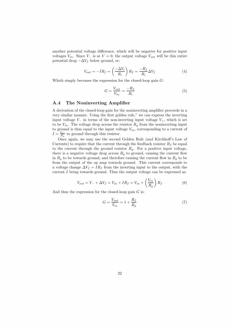
another potential voltage difference, which will be negative for positive inputvoltages Vin. Since V− is at V = 0, the output voltage Vout will be this entirepotential drop −∆Vf below ground, or:
Vout = −IRf =
(
−∆Vi
Ri
)
Rf =−Rf
Ri
∆Vf (4)
Which simply becomes the expression for the closed-loop gain G:
G =Vout
Vin
=−Rf
Ri
(5)
A.4 The Noninverting Amplifier
A derivation of the closed-loop gain for the noninverting amplifier proceeds in avery similar manner. Using the first golden rule,” we can express the invertinginput voltage V− in terms of the non-inverting input voltage V+, which is setto be Vin. The voltage drop across the resistor Rg from the noninverting inputto ground is thus equal to the input voltage Vin, corresponding to a current ofI = Vin
Rgto ground through this resistor.
Once again, we may use the second Golden Rule (and Kirchhoff’s Law ofCurrents) to require that the current through the feedback resistor Rf be equalto the current through the ground resistor Rg. For a positive input voltage,there is a negative voltage drop across Rg to ground, causing the current flowin Rg to be towards ground, and therefore causing the current flow in Rg to befrom the output of the op amp towards ground. This current corresponds toa voltage change ∆Vf = IRf from the inverting input to the output, with thecurrent I being towards ground. Thus the output voltage can be expressed as:
Vout = V− + ∆Vf = Vin + IRf = Vin +
(
Vin
Rg
)
Rf (6)
And thus the expression for the closed-loop gain G is:
G =Vout
Vin
= 1 +Rf
Rg
(7)
22

B The Laser Lock System
The laser locking system that will incorporate the photodetectors describedin this report uses the techniques of Doppler-free saturated absorption spec-troscopy and phase-sensitive detection to provide the necessary feedback loopto lock the laser wavelengths to the desired atomic line. This appendix willprovide a (very) brief and qualitative description of these techniques—withoutgoing into much detail and without the use of any equations—which was foundto be too long for the main text of this report.
B.1 Doppler-free Saturated Absorption Spectroscopy
Standard absorption spectroscopy involves the use of a single laser beam passingthrough a gas cell, with the absorption at each wavelength determined from theintensity of the beam that has passed through the cell. Due to the thermaldistribution of velocity of the gas atoms inside the cell, each atom will “see” itslines at Doppler-shifted wavelengths, and the absorption lines will be Doppler-
broadened, preventing accurate measurements of the atomic line.One way to circumvent this broadening is to use two counterpropagating
laser beams of the same frequency—a pump beam and a probe beam—with onebeam (the pump beam) being more intense than the other. With the two beamsaligned in such an antiparallel configuration, only the atoms moving entirelyorthogonal to the beams will see both beams at the same unshifted frequency, asany atom with a transverse velocity will see the beams with different frequencies.
When the pump beam is sufficiently intense that the excited state whosetransition corresponds to a given line has been saturated, such that the atomscan absorb no more photons at that frequency for the lifetime of the state,then the probe beam will see an decrease in absorption at that frequency. Thephotodetectors described in this report will measure the intensity of the pumpand probe beams, and the difference of the probe beam signal from the pumpbeam signal (provided by the photodetectors) will show a “Lamb dip” at thecorrect atomic lines, unbroadened by Doppler shifts. This is known as Doppler-free saturated absorption spectroscopy [11].
B.2 Phase Sensitive Detection
While this saturated absorption spectroscopic technique alone is sufficient forobservation of atomic lines, this experiment requires not that we observe suchlines, but that we lock the frequency of our laser to them. In order to actuallylock the beams to the line, a modification of the setup is required.
To provide the locking of the beams, the frequency of the laser light is mod-ulated by passing it through an acousto-optic modulator (AOM). In the AOM,light Bragg-diffracts off of acoustic waves in a crystal, generated by a piezoelec-tric element (a piezo). The diffracted beam separates (spatially) into discretediffraction orders, whose frequencies are determined by the modulation of the
23

piezo. By selecting one such diffraction order, and varying the modulation ofthe piezo, one may modulate the frequency of the lasers.
For the locking system, the frequencies of the pump and probe beams aretogether modulated (using the AOM) over a small range 18 back and forth.The same saturated absorption technique is applied with the modulated beams,and the inverse of the difference of the probe beam signal from the pump beamsignal is considered, such that a peak (rather than a Lamb dip) is observed atthe atomic resonance. When the “center frequency” of the two beams beforemodulation is slightly below the atomic line, and when the modulated frequencyis increasing, the inverted difference signal is also increasing, and vice versa; thatis, the signals are in phase. The converse is true for center frequencies abovethe atomic line—the signals have opposite phases.
When these signals are multiplied electronically, the result is positive (sincethe signals are in phase) for laser frequencies below the line, and negative forthose above the line. This technique, known as phase sensitive detection, givesthe required direction the wavelength needs to change, and provides the feedbacknecessary to lock the lasers to the line.
18Around 100 kHz, compared to the atomic line width of several MHz
24
C The Photodetector Enclosure
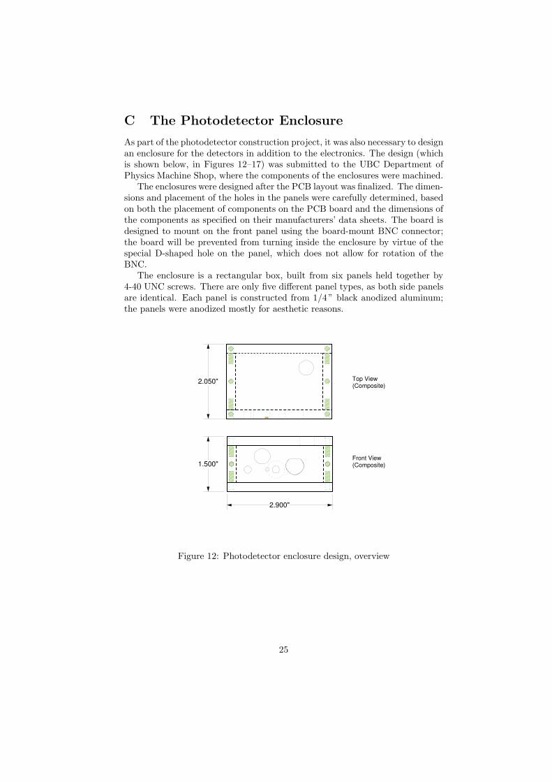
As part of the photodetector construction project, it was also necessary to designan enclosure for the detectors in addition to the electronics. The design (whichis shown below, in Figures 12–17) was submitted to the UBC Department ofPhysics Machine Shop, where the components of the enclosures were machined.
The enclosures were designed after the PCB layout was finalized. The dimen-sions and placement of the holes in the panels were carefully determined, basedon both the placement of components on the PCB board and the dimensions ofthe components as specified on their manufacturers’ data sheets. The board isdesigned to mount on the front panel using the board-mount BNC connector;the board will be prevented from turning inside the enclosure by virtue of thespecial D-shaped hole on the panel, which does not allow for rotation of theBNC.
The enclosure is a rectangular box, built from six panels held together by4-40 UNC screws. There are only five different panel types, as both side panelsare identical. Each panel is constructed from 1/4” black anodized aluminum;the panels were anodized mostly for aesthetic reasons.
Top View (Composite)
Front View (Composite)
2.050"
1.500"
2.900"
Figure 12: Photodetector enclosure design, overview
25

1/8"
1/8"
Photodetector Enclosure: Front Panel
5/8"
1 3/8"
2 7/8"
1"
1/8"
1/8"
1 7/8"
1/8"
1/8"
1"
1/4"
2 7/8"
C
DE
C D E
A A
AA
2*B 2*B
B
B
B B
Top View
Front View
3/8"
3/8"
1/2"
1/2"
Figure 1
D E
Figure 2
H1/4"3/8"
2 3/4"
3/4" 1/2"
H
1/8"
1/8"
1/4"
1/4"
1/4"
1/8"
1/2"1/2"
G
3/4"
3/4"
1/4"
H: Ø .094" hole, ~.050" deep (locking ring cutout, cuts into G)
G: special counterbored hole for a switch (see Fig. 3)
1 1/8"
1 5/8"
Figure 3
1/2"
1/4"
1/4"
Top
Side
1/2"
Back
Ø 1/4"
Ø 1/2"
G
A: 4-40 UNC counterbored clearance hole, 0.250"
E: Ø .490" special D-shaped hole, .25" deep (see Fig. 2) D: Ø .435" special D-shaped hole,
.25" deep (see Fig. 1)
B: 4-40 UNC tapped hole, .300"
C: Ø .2" hole, .25" deep
Figure 13: Photodetector enclosure design, front panel
26

Top View
Front View
Photodetector Enclosure: Bottom Plate
2 7/8"
2"
1/4"
2 7/8"
A A
AA
A A
1/8" 1/8"
1/8"
1/8" 1/8"
1" 1"
1/8" 1/8"
1/8"
1/8" 1/8"
3*A 3*A
A: 4-40 UNC counterbored clearance hole, 0.250"
1 7/8"
1"
2 3/4"
2 3/4"
2 3/4"
Figure 14: Photodetector enclosure design, bottom plate
Photodetector Enclosure: Top Plate
Top View
Front View
3/4"
5/8"
2 7/8"
2"
1/4"
2 7/8"
3/4"
1"
1/8"
1/8"
1/8"
1/8"
1"
1/8"
1/8"
3*A
A
A
A A
A
A
F
F 3*A
2 1/4"
2 3/4"
F: Ø .400" hole, .25" deep
A: 4-40 UNC counterbored clearance hole, 0.250"
2 1/4"
Figure 15: Photodetector enclosure design, top plate
27

Photodetector Enclosure: Rear Plate
1/4"1/2"
2 7/8"
2 7/8"
1/8"
1/4"
1/8"
1/4"
1"
A A
A A
2*B 2*B
B
B
B
B
B: 4-40 UNC tapped hole, .300"
Top View
Front View
1/8"
2 3/4"
2 3/4"
3/4"
1/4"
3/4"
1/4"
1/2"
1/8"
2 3/4"
A: 4-40 UNC counterbored clearance hole, 0.250"
Figure 16: Photodetector enclosure design, rear plate
Photodetector Enclosure: Side Panels
1"
1 1/2"
1 1/2"
3/4"
3/4"
1"
1/4"
1/4"1/2"
1/4"
3/4"
2*B
2*B
B
B B
B
B
B
B
B
B: 4-40 UNC tapped hole, .300"
Top View
Side View Front View
1/4"3/4"
1/4"
1 1/4"
1/8"
1/8"
1/4"
1 1/4"
1/8"
1/8"
3/4"1/2"1/2"
Figure 17: Photodetector enclosure design, side panels
28

D List of Equipment
The following list is not an exhaustive compilation of everything that was used,but rather a list of the products and equipment were most important or mostrelevant throughout the design, testing, and construction of the photodetectors.
D.1 Design and Data Analysis Software
Product Brand & Model
Electronics design Altium (Protel) CircuitStudio 2004Electronics design CadSoft EAGLE Light Edition 4.1Electronics/mechanical design MiniCAD VectorWorks 8.5.2Data analysis Wolfram Research Mathematica 4
Table 1: Software used for design, layout, and data analysis.
D.2 Electrical/Optical Measurement Equipment
Product Brand & Model
Digital multimeter Extech Instruments 380282Digital oscilloscope Tektronix TDS3014High-speed photodetector Thorlabs PDA155Laser power detector Coherent FieldMaster-GSOptical spectrum analyzer Ando AQ-6315A
Table 2: Equipment used for electrical and optical measurements.
D.3 Laser Equipment
Product Brand & Model
Helium-Neon laser 1 mW HeNe at 633 nm, unknown originLaser diode NVG Inc. model D660-5, 5 mW at 660 nmCollimation tube Thorlabs LT230P-B collimation tube
Table 3: Laser equipment used for testing.
29

D.4 Power Supplies and Signal Sources
Product Brand & Model
Function generator (3 MHz) Interstate Electronics Corp. F33Function generator (20 MHz) BK Precision 4040ASynthesized signal generator (1 GHz) Agilent 8648ABreadboard w/ power supply K&H Projects PP-272Power supply (±15 V, floating 5 V) Power-One CP131-A
Table 4: Power supplies and signal sources used.
D.5 Soldering and Assembly Equipment
Product Brand & Model
Soldering iron Weller TC201PSoldering tip Weller PTA8 (screwdriver)Soldering tip Weller PTS7 (long conical)Soldering system Metcal MX-500SSoldering tip Metcal STTC-537 (chisel)Soldering tip Metcal STTC-507 (conical)Soldering tip Metcal STTC-540 (bent)Hot air rework station Atten 850Carbide drill bits Drill Bit City, #68Carbide drill bits Drill Bit City, #71
Table 5: Equipment for soldering and assembling boards.
D.6 PCB Processing Equipment and Supplies
Product Brand & Model
Etching tank, air pump, & heater Circuit Specialists ET10 Etching SystemPCB exposure fluorescent light MG Chemicals 416-X Exposure KitPCB developer (NaOH) MG Chemicals #418 DeveloperPCB etchant MG Chemicals Ammonium Persulphate
Table 6: PCB processing chemicals and equipment.
30

E List of Vendors
Much of the equipment and supplies used in this project were already availablein the lab before the project commenced. However, all of the electronics com-ponents (as well as some equipment and supplies) used in this project needed tobe ordered (and reordered). Additionally, some components (i.e. the enclosurefor the photodetector) needed to be machined or manufactured. These wereeach obtained from the vendors, distributors, and other businesses in Table 7:
Vendor Products / Services URL or Location
Allied Electronics Electronics components http://www.alliedelec.comDigiKey Electronics components http://www.digikey.caElectrosonic Electronics components http://www.e-sonic.caMouser Electronics components http://www.mouser.comNewark InOne Electronics components http://canada.newark.comHamamatsu Optoelectronics http://www.hamamatsu.comDrill Bit City Carbide drill bits http://www.drillbitcity.comUBC Physics Ma-chine Shop
Enclosure machining Hennings Building, UBC
UBC PhysicsElectronics Lab
Electronics components Hennings Building, UBC
Table 7: A list of vendors, distributors, and other businesses used
31

Bibliography
[1] Jeremy Bernstein, Paul Fishbane, and Stephen Gasiorowicz. Modern
Physics. Prentice Hall, 2000.
[2] Burr-Brown. OPA686 Datasheet, September 2000.
[3] Doug DeMaw. Practical RF design manual. Prentice-Hall, EnglewoodCliffs, N.J., 1982.
[4] Luke Enriquez. Hints and tips for using surface mount technology. Anonline guide to SMT, found at http://www.geocities.com/vk3em, August2001.
[5] Jeremy Everard. Fundamentals of RF Circuit Design: with Low Noise
Oscillators. John Wiley and Sons, Chichester, 2001.
[6] Paul Horowitz and Winfield Hill. The Art of Electronics. Cambridge Uni-versity Press, Cambridge, second edition, 1989.
[7] JILA Electronics Lab. 2-Stage Photodetector Circuit Schematic, June 2002.
[8] Todd P. Meyrath. A simple photodiode amplifier. A design for a photodiodeamplifier, with notes, schematics, and a PCB mask, April 2004.
[9] John H. Moore, Davis C. Christopher, and Michael A. Coplan. Build-
ing Scientific Apparatus: A Practical Guide to Design and Construction.Westview Press, Redwood City, Calif., second edition, 1989.
[10] Roberto Onofrio and Carlo Presilla. Ultracold atomic fermi-bose mixturesin bichromatic optical dipole traps: a novel route to study fermion super-fluidity. Journal of Statistical Physics, 115(1-2):57–89, 2004.
[11] Daryl W. Preston. Doppler-free saturated absorption: Laser spectroscopy.American Journal of Physics, 64(11):1432–1436, 1996.
[12] Volker Schweikhard. Ultracold Atoms in a Far Detuned Optical Lattice.PhD thesis, Physikalisches Institut, Universitat Stuttgart, November 2001.
[13] Peter van der Straten and Harold Metcalf. The quest for bec. In Claus Zim-mermann Matthias Weidemller, editor, Interactions in Ultracold Gases:
From Atoms to Molecules, pages 1–63. WileyEurope, March 2003.
32