the dc and ac withstands test for tps booster injection kicker
TRANSCRIPT
THE DC AND AC WITHSTANDS TEST FOR TPS BOOSTER INJECTION KICKER *
Yung-Hui Liu#, Chin-Shen Chen, Che-Kai Chan, Ying-Tzu Huang, Chih-Sheng Yang, Hsin-Hui Chen, June-Rong Chen, NSRRC, Hsinchu, Taiwan
Abstract TPS requires highly precise and stable pulsed magnets
for top-up mode operation. One injection and two extraction in vacuum kicker magnets in the booster ring are designed and noticed to minimize driving voltage. The HV insulation for magnet itself and vacuum feedthrough need to be tested. A DC withstand voltage tester MUSASHI 3802 (Model: IP-701G) is used to test the DC breakdown voltage, which the maximum driving voltage is 37 kV. And the AC withstand voltage tester (PHENIX AC dielectric tester, Model 6CP100/50-7.5-220) was also test the AC breakdown voltage. Thicker than 10 mm ceramic plate could effectively avoid the breakdown occurred with 37 kV DC charging. Thus HV withstand voltage will be higher in vacuum chamber and the insulation with HV will not be the problem.
INTRODUCTION The Taiwan photon source (TPS) requires highly
precise and stable pulsed magnets for top-up mode operation [1]. Ten pulsed magnets are used for injection and extraction of the electron beam in the booster and storage ring [2]. One injection and two extraction in vacuum kicker magnets in the booster ring are designed for minimizing driving voltage. The HV insulation, vacuum feedthrough, and air pressure condition need to be noticed. The electron beam of the booster synchrotron is injected from 150-MeV LINAC and accelerated to operating energy 3 GeV with 3 Hz repetition rate. The beam at full energy is then transferred through the transfer line to the storage ring. According to the booster design, the electron beam is injected into the booster synchrotron along the axis, involving an injection septum (length 0.8 m) and a quick kicker magnet (length 0.5 m) to place the beam on that booster axis. After the electron beam is ramped to 3 GeV, the beam at full energy is extracted from the booster in one turn period using two kicker magnets (effective length 1.0 m) and septa (0.8 m DC and 0.8 m AC septum).
TPS BOOSTER KICKER SPECIFICATIONS
The pulsed magnets in TPS are divided into 3 parts. The first part is booster injection section; there are one booster injection septum and one kicker included. Then,
the electron beam extract to the second part - booster extraction section. There are 2 booster extraction kickers and two septa (DC+AC septum) in booster extraction section. Passing by the BTS (booster to storage ring) section, the electron beam is inject to the storage ring by 4 kickers and two septa (Pre AC septum +AC septum). The booster kickers, including one injection and 2 extraction ones, were all rectangular wave type.
Table 1 showed the parameters of booster injection and extraction kickers. Because of the concentric design for booster ring, the length of bunch train could reach up to 1000 ns. The fall time for BR injection kicker and rise time for extraction kicker is set to be 350 ns within one revolution time. The maximum value for extraction kicker is reach to 30 kV(shown in brackets), this will be severe requirement. The impedance of pulser is 25 for 2 standard parallel 50 cables. The flatness for the flat top is ± 1% and the pulse to pulse stability is within ± 0.1%.
Table 1: Booster Kicker Specifications
Specifications Booster kicker
Injection Extraction (2 pieces)
Electron energy (GeV) 0.15 3.0 Bend angle (mrad) 16 [30] 1.3 [2.0] Beam aperture (mm) 35*20 35*18 Length (m) 0.5 0.5 * 2 Nominal field (T) 0.016 [0.03] 0.026 [0.04] Mag. aperture (mm) 65*20 65*18 Nominal current (A) 267 [501] 372 [573] Pulse shape Flat top Flat top Fall time (ns) 95%-5% <350 <350 Pulse duration (ns) 1000ns-FT 1000ns-FT Energy in magnet (J) 0.100 [0.352] 0.208 [0.492] Impedance (Ohm) 25 25 Inductance (H) 2.8 3.0 Drive voltage (kV) 13.4 [25.1] 18.6 [28.6] Pulse to pulse stability(%) ± 0.1 ± 0.1 Flatness (%) ± 1 ± 1
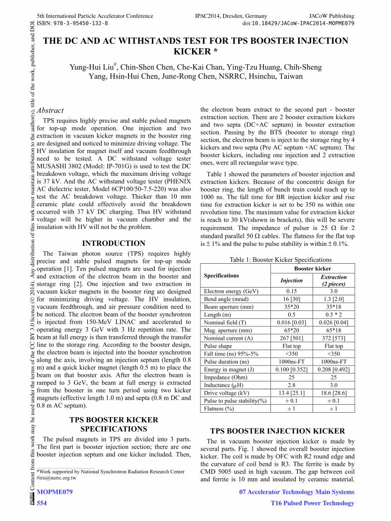
TPS BOOSTER INJECTION KICKER The in vacuum booster injection kicker is made by
several parts. Fig. 1 showed the overall booster injection kicker. The coil is made by OFC with R2 round edge and the curvature of coil bend is R3. The ferrite is made by CMD 5005 used in high vacuum. The gap between coil and ferrite is 10 mm and insulated by ceramic material.
___________________________________________
*Work supported by National Synchrotron Radiation Research Center #[email protected]
5th International Particle Accelerator Conference IPAC2014, Dresden, Germany JACoW PublishingISBN: 978-3-95450-132-8 doi:10.18429/JACoW-IPAC2014-MOPME079
MOPME079554
Cont
entf
rom
this
wor
km
aybe
used
unde
rthe
term
soft
heCC
BY3.
0lic
ence
(©20
14).
Any
distr
ibut
ion
ofth
isw
ork
mus
tmai
ntai
nat
tribu
tion
toth
eau
thor
(s),
title
ofth
ew
ork,
publ
isher
,and
DO
I.
07 Accelerator Technology Main SystemsT16 Pulsed Power Technology
The booster injection kicker was put in a 350 CF chamber, which is fixed on the wall. The outgas rate from ferrite (total surface area 1680 cm2) and insulators (ceramic) will increase outgassing rate. Baking at 150 oC for 24 hr could reduce outgassing rate, which could satisfy the design requirement of booster vacuum [3]. Two inlet and two outgo feedthroughs were need in the booster injection kicker. The 75 CF flange was used and two RG-220 cables (standard 50 ) were used to connect the pulser and kicker.
Figure 1: The Booster injection kicker magnet system.
ELECTRODE EDGE AND GAP BETWEEN ELECTRODE AND GROUND
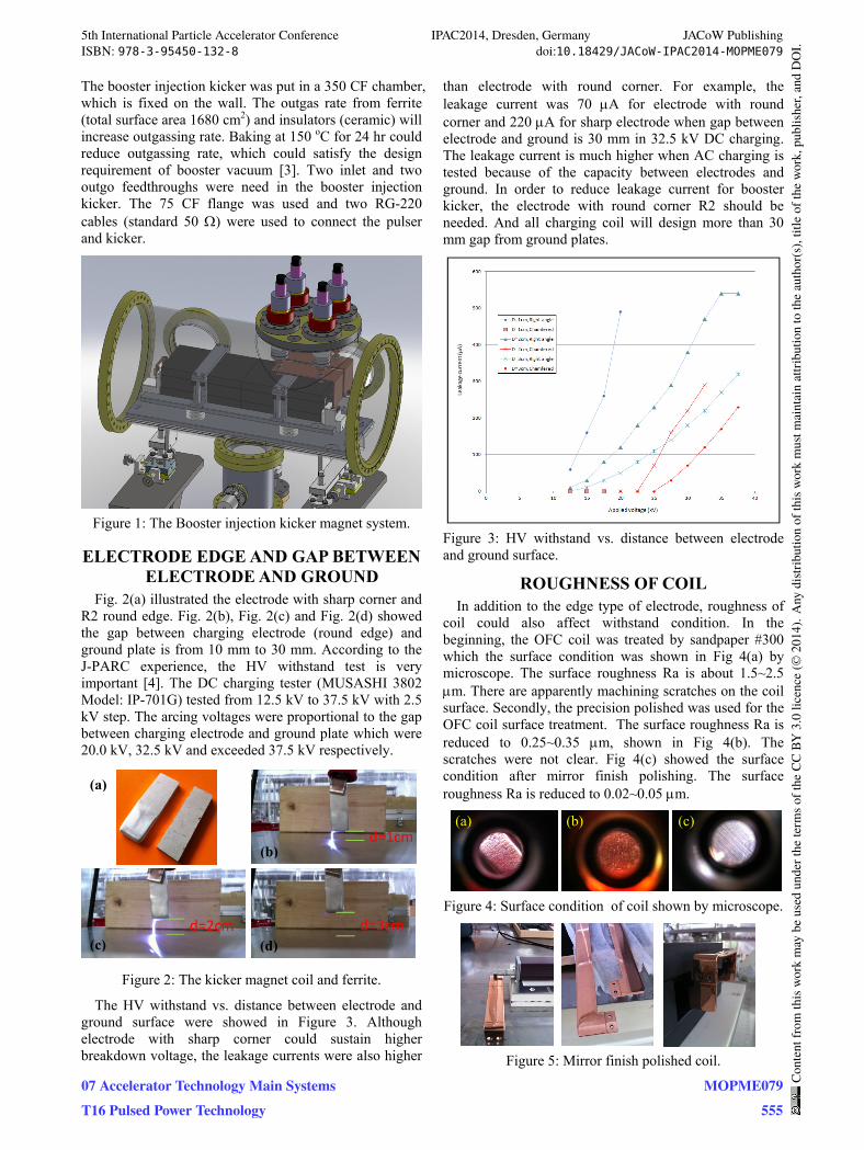
Fig. 2(a) illustrated the electrode with sharp corner and R2 round edge. Fig. 2(b), Fig. 2(c) and Fig. 2(d) showed the gap between charging electrode (round edge) and ground plate is from 10 mm to 30 mm. According to the J-PARC experience, the HV withstand test is very important [4]. The DC charging tester (MUSASHI 3802 Model: IP-701G) tested from 12.5 kV to 37.5 kV with 2.5 kV step. The arcing voltages were proportional to the gap between charging electrode and ground plate which were 20.0 kV, 32.5 kV and exceeded 37.5 kV respectively.
Figure 2: The kicker magnet coil and ferrite.
The HV withstand vs. distance between electrode and ground surface were showed in Figure 3. Although electrode with sharp corner could sustain higher breakdown voltage, the leakage currents were also higher
than electrode with round corner. For example, the leakage current was 70 A for electrode with round corner and 220 A for sharp electrode when gap between electrode and ground is 30 mm in 32.5 kV DC charging. The leakage current is much higher when AC charging is tested because of the capacity between electrodes and ground. In order to reduce leakage current for booster kicker, the electrode with round corner R2 should be needed. And all charging coil will design more than 30 mm gap from ground plates.
Figure 3: HV withstand vs. distance between electrode and ground surface.
ROUGHNESS OF COIL In addition to the edge type of electrode, roughness of
coil could also affect withstand condition. In the beginning, the OFC coil was treated by sandpaper #300 which the surface condition was shown in Fig 4(a) by microscope. The surface roughness Ra is about 1.5~2.5 m. There are apparently machining scratches on the coil surface. Secondly, the precision polished was used for the OFC coil surface treatment. The surface roughness Ra is reduced to 0.25~0.35 m, shown in Fig 4(b). The scratches were not clear. Fig 4(c) showed the surface condition after mirror finish polishing. The surface roughness Ra is reduced to 0.02~0.05 m.
Figure 4: Surface condition of coil shown by microscope.
Figure 5: Mirror finish polished coil.
(a)
(b) d=1cm
(c) d=2cm d=3cm
(d)
(a) (b) (c)
5th International Particle Accelerator Conference IPAC2014, Dresden, Germany JACoW PublishingISBN: 978-3-95450-132-8 doi:10.18429/JACoW-IPAC2014-MOPME079
07 Accelerator Technology Main SystemsT16 Pulsed Power Technology
MOPME079555
Cont
entf
rom
this
wor
km
aybe
used
unde
rthe
term
soft
heCC
BY3.
0lic
ence
(©20
14).
Any
distr
ibut
ion
ofth
isw
ork
mus
tmai
ntai
nat
tribu
tion
toth
eau
thor
(s),
title
ofth
ew
ork,
publ
isher
,and
DO
I.
The final surface of OFC coil was shown in Fig. 5 which were mirror finish polished. The AC withstand tester (PHENIX Model 6CP100/50-7.5-220) measured AC withstands for different surface roughness of coil, which the gap is 35 mm. The AC withstand was 22.5 kV for coil was treated by sandpaper #300. And the AC withstand was increased to 25.0 kV for coil was treated by precision polished. The AC withstand was increased to 30.0 kV for coil was treated by mirror finish polishing. Not only the AC withstands increase, but leakage current reduce by reducing roughness of the coil surface.
BOOSTER INJECTION KICKER WITHSTANDS TESTS
Although the nominal driving voltage for booster injection kicker is 13.4 kV and the maximum voltage is 25.1 kV, the DC withstand test was still tested up to 35 kV [5]. Because of the structure is similar to booster extraction kicker which the maximum driving voltage is 28.6 kV, the same design could apply to the booster extraction kicker.
Figure 6: The experimental setup for DC withstand voltage test.
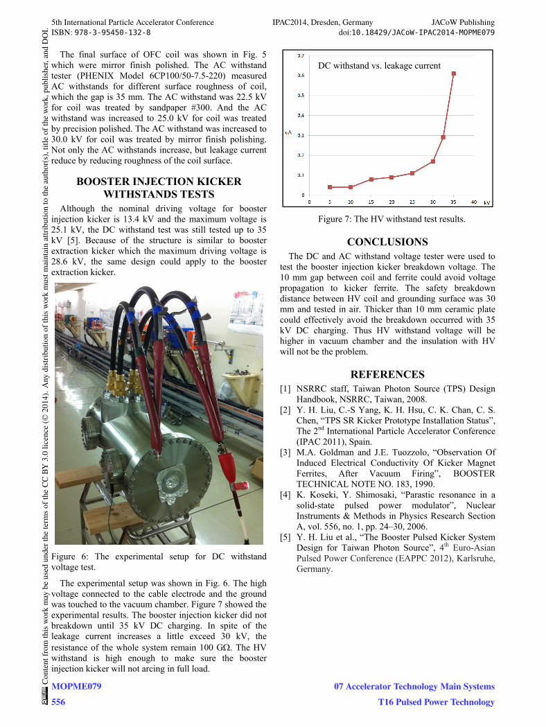
The experimental setup was shown in Fig. 6. The high voltage connected to the cable electrode and the ground was touched to the vacuum chamber. Figure 7 showed the experimental results. The booster injection kicker did not breakdown until 35 kV DC charging. In spite of the leakage current increases a little exceed 30 kV, the resistance of the whole system remain 100 G. The HV withstand is high enough to make sure the booster injection kicker will not arcing in full load.
Figure 7: The HV withstand test results.
CONCLUSIONS The DC and AC withstand voltage tester were used to
test the booster injection kicker breakdown voltage. The 10 mm gap between coil and ferrite could avoid voltage propagation to kicker ferrite. The safety breakdown distance between HV coil and grounding surface was 30 mm and tested in air. Thicker than 10 mm ceramic plate could effectively avoid the breakdown occurred with 35 kV DC charging. Thus HV withstand voltage will be higher in vacuum chamber and the insulation with HV will not be the problem.
REFERENCES [1] NSRRC staff, Taiwan Photon Source (TPS) Design
Handbook, NSRRC, Taiwan, 2008. [2] Y. H. Liu, C.-S Yang, K. H. Hsu, C. K. Chan, C. S.
Chen, “TPS SR Kicker Prototype Installation Status”, The 2nd International Particle Accelerator Conference (IPAC 2011), Spain.
[3] M.A. Goldman and J.E. Tuozzolo, “Observation Of Induced Electrical Conductivity Of Kicker Magnet Ferrites, After Vacuum Firing”, BOOSTER TECHNICAL NOTE NO. 183, 1990.
[4] K. Koseki, Y. Shimosaki, “Parastic resonance in a solid-state pulsed power modulator”, Nuclear Instruments & Methods in Physics Research Section A, vol. 556, no. 1, pp. 24–30, 2006.
[5] Y. H. Liu et al., “The Booster Pulsed Kicker System Design for Taiwan Photon Source”, 4th Euro-Asian Pulsed Power Conference (EAPPC 2012), Karlsruhe, Germany.
DC withstand vs. leakage current
5th International Particle Accelerator Conference IPAC2014, Dresden, Germany JACoW PublishingISBN: 978-3-95450-132-8 doi:10.18429/JACoW-IPAC2014-MOPME079
MOPME079556
Cont
entf
rom
this
wor
km
aybe
used
unde
rthe
term
soft
heCC
BY3.
0lic
ence
(©20
14).
Any
distr
ibut
ion
ofth
isw
ork
mus
tmai
ntai
nat
tribu
tion
toth
eau
thor
(s),
title
ofth
ew
ork,
publ
isher
,and
DO
I.
07 Accelerator Technology Main SystemsT16 Pulsed Power Technology