the compliance information resource … 11: a historical and evolutionary review daniel d. hoolihan...
TRANSCRIPT
AUGUST 2010
A HISTORICAL AND EVOLUTIONARY REVIEW
MagazineTHE COMPLIANCE INFORMATION RESOURCE FOR ELECTRICAL ENGINEERS
CISPR 11
IN Compliance MagazinePO Box 235Hopedale, MA 01747CHANGE SERVICE REQUESTED
TM

August 2010 IN Compliance 3
WHAT’S INSIDE
BUSINESS NEWS47
18 ALL FERRITE BEADS ARE NOT CREATED EQUAL Understanding the Importance of Ferrite Bead Material BehaviorChris Burket, TDK Corporation
LACK OF GLOBAL STANDARDIZATION Directly Impacts Market AccessBill Holz, TÜV Rheinland of North America
Simulating Small Device CDM USING SPICERobert Ashton, ON Semiconductor; Marty Johnson, National Instruments; Scott Ward, Texas Instruments
FUNDAMENTALS OF ELECTROSTATIC DISCHARGE Part 1: An Introduction to ESDThe ESD Association
8
EVENTS50
NEWS IN COMPLIANCE5
THE FUTURE OF EMC ENGINEERING37
28
32
38
CISPR 11: A Historical and Evolutionary ReviewDaniel D. Hoolihan
COMPONENTS DIRECTORY46

4 IN Compliance August 2010 www.incompliancemag.com
Lorie NicholsPublisher & Editor
Sharon SmithDirector of Sales
Barbara KovalchekMedia Consultant
Erin C. FeeneyDirector of Media Services
IN Compliance MagazineISSN 1948-8254 (print)
ISSN 1948-8262 (online)
is published by
Same Page Publishing LLCP.O. Box 235
Hopedale, MA 01747tel: (508) 488-6274fax: (508) 488-6114
IN Compliance Magazine subscriptions are free to qualified subscribers in North America.
Subscriptions outside North America are $129 for 12 issues. The Digital Edition is free.
Please contact our circulation department at [email protected]
For information about advertising with IN Compliance, please call 978-873-7722 or
e-mail [email protected].
Copyright 2010 IN Compliance Magazine, all rights reserved.
Contents may not be reproduced in any form without the prior consent of the publisher.
While every attempt is made to provide accurate information, neither the publisher nor the authors
accept any liability for errors or omissions.
Magazine

August 2010 IN Compliance 5
NEWS IN COMPLIANCE
FCC Seeks Comments on Interoperability in 700 MHz Band
The Federal Communications Commission (FCC) has requested additional comments in connection with its efforts to expand deployment of public safety broadband networks in the 700 MHz band.
In a Public Notice issued in May, the Commission detailed several key technical issues related to the interoperability of individual networks within a nationwide public safety broadband system. These technical issues include whether or not to allow roaming between public safety and commercial networks, what security features (if any) should be supported to optimize network security, and what requirements for performance and reliability should be adopted for the network or devices utilized on the network.
In addition to these and other interoperability technical issues, the Commission has also requested comments on matters related to out-of-band emissions limits and equipment certification requirements.
Although comments on the issues raised in the Commission’s Public Notice were due by mid-June, the Public Notice provides an in-depth look at the Commission’s thinking related to the deployment of a nationwide broadband network for public safety
communications. The complete text of the Public Notice is available at http://hraunfoss.fcc.gov/edocs_public/attachmatch/DA-10-884A1.pdf.
FCC Clamps Down on Violations of HAC Requirements
The Federal Communications Commission (FCC) is continuing its strict enforcement of its hearing aid compatibility (HAC) requirements for manufacturers and service providers of wireless equipment and services, as evidenced by a recent flurry of enforcement actions.
In late May, the Commission issued citations to eight separate resellers of wireless services for failing to file annual hearing aid compatibility status reports as required under the FCC’s 2003 Hearing Aid Compatibility Order. In the same time frame, the Commission also announced that it had resolved four separate petitions for requests for waiver of obligations under the hearing aid compatibility requirements.
The circumstances prompting each of the citations were unique, but recipients generally claimed that they failed to file the required reports because they either did not know of the requirement, or believed that the requirement did not apply to them. However, in each and every case, the Commission reiterated that its HAC reporting requirements apply to all wireless service providers, including resellers.
Commission Citations carry no financial penalties, but represent a final warning of sorts to their recipients, and violations of FCC regulations subsequent to receipt of a Citation can lead to monetary forfeitures up to $150,000 for each violation, or for each day of a continuing violation.
The complete text of the FCC’s citation against eCallPlus (one of the eight recipients of citations in May) can be viewed at http://hraunfoss.fcc.gov/edocs_public/attachmatch/DA-10-932A1.pdf.
FCC Opens Formal Inquiry on Legal Framework for Broadband
The Federal Communications Commission (FCC) has opened a formal inquiry seeking comments on its recently released proposal to revamp its regulation of the Internet and Internet services.
In a Notice of Inquiry issued in June, the Commission has requested comments on a new regulatory framework for broadband Internet services, first outlined by FCC Chairman Julius Genachowski in May. In brief, Genachowski’s so-called “third-way” to regulating the Internet reportedly attempts to strike a balance between the Commission’s current regulatory framework and a more highly regulated scenario by creating a precise policy for the regulation of broadband services.
DILBERT: © Scott Adams/Dist. by United Feature Syndicate, Inc. Reprinted with permission.

6 IN Compliance August 2010 www.incompliancemag.com
NEWS IN COMPLIANCE
The Commission’s long-standing approach to regulating broadband Internet services was struck a significant blow in April, when the Federal Court of Appeals for the District of Columbia Circuit determined that the Commission exceeded its statutory authority when it sanctioned Comcast Corporation back in 2008. The Court, in overturning the Commission’s action against Comcast, ruled that Congress had not accorded the FCC the power to regulate the network management practices of Internet service providers. Comments on the Commission’s Notice of Inquiry were due by July 15th. The complete text of the Notice is available at http://hraunfoss.fcc.gov/edocs_public/attachmatch/FCC-10-114A1.pdf.
New Standards Lists Released For the EU’s Machinery Directive
The Commission of the European Union (EU) has issued an updated list of standards that can be used to demonstrate compliance with the essential requirements of its Directive 2006/42/EC, the current version of the so-called Machinery Directive.
The EU’s Machinery Directive defines the essential health and safety requirements for a wide range of products, including machinery and partly completed machinery; lifting accessories; chains, ropes and webbing; interchangeable equipment; removable mechanical transmission devices; and safety components.
The Directive’s scope specifically excludes electrical and electronic products covered under Directive 73/23/EEC (the so-called Low Voltage Directive), including household appliances, audio and video equipment, informational technology equipment and ordinary office machinery.
The extensive list of CEN and CENELEC standards for the Machinery Directive was published in May in the
Official Journal of the European Union and replaces all previously published standards lists for the Directive.
The revised list of standards can be viewed at http://eur-lex.europa.eu/LexUriServ/LexUriServ.do?uri=OJ:C:2010:136:0001:0041:EN:PDF. A brief correction to the May 26th listing, published on June 11th, is available at http://eur-lex.europa.eu/LexUriServ/LexUriServ.do?uri=OJ:C:2010:152: 0014:0014:EN:PDF.
EU Parliament Renews Concerns About EMFs
The European Union (EU) Parliament has formally adopted a resolution calling on the EU Commission and other parties to speed research into possible adverse health effects associated with exposure to electromagnetic fields (EMFs).
The resolution, which was originally presented to the Parliament in April 2009, but just published in May 2010 in the Official Journal of the European Union, calls on the Commission to “present a yearly report on the level of electromagnetic radiation in the EU, its sources, and actions taken in the EU to better protect human health and the environment.”
Covering a large number of issues related to EMF exposure, the Parliament’s resolution articulates pointed concerns about increasing exposure to EMFs from the use of mobile phones, especially among children and young adults. On that issue, the resolution specifically “condemns certain particularly aggressive marketing campaigns by telephone operators” that feature “mobile phones designed solely for children or free call time packages aimed at teenagers.”
Further, the resolution sharply questions the extended delay in the release of findings from the so-called Interphone epidemiological study,
intended to explore possible links between the use of mobile phones and certain types of cancers. (Results from this study, conducted earlier in the decade, were expected to be released in 2006, according to the Parliament’s resolution.)
The complete text of the Parliament’s resolution regarding EMFs is available at http://eur-lex.europa.eu/LexUriServ/LexUriServ.do?uri=OJ:C:2010:137E: 0038:0042:EN:PDF.
European Union Recasts Energy Labeling Requirements Directive
In support of the European Union’s (EU’s) stated goal of achieving a 20% savings in energy consumption by 2020, the EU Commission has published a “recast” version of its directive on the labeling of energy-consuming products.
The new directive, 2010/30/EU, covers “labeling and standards product information on the consumption of energy and other resources by energy-related products,” and is intended to establish a framework for the harmonization of national regulations on information provided to end users.
Published in June in the Official Journal of the European Union, the new directive provides regulators, manufacturers and other interested parties with a single document that consolidates the numerous amendments that have been made to the original energy labeling directive, 92/75/EEC, issued in 1992. More important, the scope of the new directive has been expanded beyond household appliances (the focus of 92/75/EEC) to cover all “energy-related products which have a significant direct or indirect impact on the consumption of energy.” Indeed, the directive’s only named exclusion from its provisions is for “second-hand products.”
EU Member States have until June 20, 2011 to integrate the provisions of

August 2010 IN Compliance 7
NEWS IN COMPLIANCE
the new directive into their respective national laws and regulations. The former directive, 92/75/EEC will then be repealed, effective July 21, 2011.
The complete text of the EU’s new energy labeling directive is available at http://eur-lex.europa.eu/LexUriServ/LexUriServ.do?uri=OJ:L:2010:153: 0001:0012:EN:PDF.
Fire Hazard Prompts Recall of Coffee Maker
Walmart Stores of Bentonville, AR has issued a voluntary recall of about 900,000 General Electric-brand coffee makers manufactured in China.
According to a recall alert issued by the U.S. Consumer Product Safety Commission (CPSC), the coffee makers can overheat, posing fire and burn hazards to consumers.
Walmart says that it has received 83 reports of overheating, smoking, melting, burning and fire associated with the recalled coffee makers, including three reports of minor burns and one report of a significant kitchen fire with extensive damage.
The recalled coffee makers were sold exclusively at Walmart stores nationwide from March 2008 through January 2010 for about $30.
To view the CPSC notice regarding this recall, go to http://www.cpsc.gov/cpscpub/prerel/prhtml10/10238.html.
Hewlett-Packard Expands Notebook Battery Recall
Hewlett-Packard of Palo Alto, CA has expanded its voluntary recall of lithium-ion batteries manufactured in China and used in certain HP and Compaq-brand notebook computers.
According to the U.S. Consumer Product Safety Commission (CPSC), the
recalled batteries can overheat, posing a fire and burn hazard to consumers.
Hewlett-Packard originally recalled about 70,000 lithium-ion batteries in May 2009. Since then, the company says that it has received 38 additional reports of batteries that overheated and ruptured, resulting in 11 instances of minor personal injury and 31 instances of minor property damage. The additional reports led the company to issue the current recall, which involves an additional 54,000 units.
The lithium-ion batteries were sold with various models of HP and Compaq notebook computers through computer and electronics stores nationwide, and through hp.com and hpshopping.com, from August 2007 through July 2008 for between $500 and $3000. The batteries were also sold separately for between $100 and $160.
To view the CPSC notice regarding this recall, go to http://www.cpsc.gov/cpscpub/prerel/prhtml10/10240.html.
Dishwashers Recalled Due to Fire Hazard
The Maytag Corporation of Newton, IA and Benton Harbor, MI has announced the voluntary recall of about 1.7 million dishwashers, due to the potential of an electrical failure in the dishwasher’s heating element.
The electrical failure can pose a serious fire hazard, according to a recall notice recently issued by the U.S. Consumer Product Safety Commission (CPSC).
Maytag has received 12 reports of dishwasher heating element failures that have resulted in fires and dishwasher damage, including a single report of an extensive kitchen fire. However, there have been no reports of injuries.
The recalled dishwashers were sold at department and appliance stores and by homebuilders nationwide from February
2006 through April 2010 for between $250 and $900.
To view the CPSC notice regarding this recall, go to http://www.cpsc.gov/cpscpub/prerel/prhtml10/10255.html.
General Electric Recalls Washing Machines
GE Appliances & Lighting of Louisville, KY is voluntarily recalling about 181,000 of its front-load washing machines manufactured in China.
According to a recall notice issued by the U.S. Consumer Product Safety Commission (CPSC), a wire within the machine can break and make contact with a metal part on the washtub while the machine is operating, posing a fire and shock hazard to consumers.
The company has received reports of seven incidents related to the recalled washing machines, in which flames escaped from the units and caused minor smoke damage. However, there have been no reports of injuries.
The recalled washing machines were sold in department and various retail stores nationwide from December 2006 through May 2010 for about $700.
Additional details regarding this recall are available at http://www.cpsc.gov/cpscpub/prerel/prhtml10/10259.html.
CISPR 11 – A Historical and Evolutionary Reviewby Daniel D. Hoolihan
CISPR 11A Historical and Evolutionary Review
by Daniel D. Hoolihan

August 2010 IN Compliance 9
CISPR 11 is the International Standard for electromagnetic emissions (disturbances) from Industrial, Scientific and Medical (ISM) Equipment.
The official title of the standard is “Industrial, Scientific, and Medical Equipment – Radio-Frequency Disturbance Characteristics – Limits and Methods of Measurement.” The premiere edition of the standard was released in 1975 and the latest edition (Edition 5.0) was released in 2009. The standard includes both limits and methods of measurement for conducted phenomena and radiated phenomena. This article traces the history and development of the content of the standard over the last 35 years.
FIRST EDITION - 1975The title of the Premiere Edition was “Limits and Methods of Measurement of Radio Interference Characteristics of Industrial, Scientific, and Medical (ISM) Radio-Frequency Equipment (excluding surgical diathermy apparatus).” The publication was prepared by CISPR Subcommittee B (Interference from Industrial, Scientific, and Medical
Apparatus). It summarized the technical content of a number of CISPR Publications, Recommendations and Reports over a period of 8 years (1967-1975).
NOTE – CISPR is the International Committee on Radio Frequency Interference; it has a number of Subcommittees that address various areas of electromagnetic interference.
The frequency range covered by the First Edition was 150 kHz to 18 GHz. The terminal voltage limits were quoted in millivolts and covered the frequency range 150 kHz to 30 MHz. Table 1(Terminal Voltage Limits) from the First Edition is reproduced in Figure 1.
The radiated limits were quoted for the frequency range 0.150 MHz to 1000 MHz and they were quoted in microvolts per meter. They were quoted at antenna-measurement distances of 30, 100, and 300 meters from the equipment or 30 meters or 100 meters from the boundary of the users’ premises.
CISPR 11 – A Histor ical and Evolut ionary Review FEATURE
Frequency Range - MHz
On a Test Site, at a distance from the
equipment of 30 m
On a Test Site, at a distance from the
equipment of 100 m
Not on a Test Site, at a Distance of 30 m from the boundary of user’s premises
Not on a Test Site, at a Distance of 100 m from the boundary of user’s premises
Not on a Test Site, at a Distance of 300 m from the equipment
0.15 – 0.285 - 50 (34) - 50 (34) -
0.285 – 0.49 - 250 (48) - 250 (48) -
0.49 – 1.605 - 50 (34) - 50 (34) -
1.605 – 3.95 - 250 (48) - 250 (48) -
3.95 – 30 - 50 (34) - 50 (34) -
30 – 470 30 (30) – In TV Bands
500 (54) – Outside TV Bands
- 30 (30)* 50 (34)** 200 (46)
470 - 1000 100 (40) – In TV Bands
500 (54) – Outside TV Bands
- 100 (40)*
500 (54)** - 200 (46)
• * - Compliance with these limits is required only for the TV channels in use at any time at the site
• ** - Limits for use outside the TV channels in use at the time at the site
Figure 2
Frequency Range - MHz Limits in mV for microwave ovens with RF power of 5 kW or less
Limits in mV for all other ISM equipment
0.15 – 0.20 2 3
0.20 – 0.50 2 2
0.50 – 5.0 1 1
5.0 – 30.0 2 1
Figure 1

10 IN Compliance August 2010 www.incompliancemag.com
FEATURE CISPR 11 – A Histor ical and Evolut ionary Review
Table II [Limits of Radiation in microvolts/meter and decibels (uV/m)] from the First Edition is recreated in Figure 2.
There was a special limit for radiation from microwave equipment used for heating and medical purposes in the frequency range from 1-18 GHz; it was 57 dB above a picowatt Effective Radiated Power (ERP) referred to a half-wave dipole.
Methods of measurement quoted CISPR Publications 1, 2, and 4 for quasi-peak measuring sets. Measurement of the radio-frequency voltage on supply mains (AC voltage lines) was done with a V-network with an intrinsic impedance of 150 ohms.
Magnetic field measurements are made with a balanced loop antenna below 30 MHz. Above 30 MHz, an “electric aerial” would be used as per CISPR Publications 2 and 4. The center of the “aerial” would be 3 meters above the ground.
Above 1 GHz, the “receiving aerial” shall be made with a directive aerial of small aperture capable of making separate measurements of the vertical and horizontal components of the radiated field. The height of the aerial had to be the same as the height of the approximate radiation center of the equipment under test.
SECOND EDITION - 1990The Second Edition was released in 1990 and it contained changes over the previous 15 years including two amendments.
In this Edition, ISM Equipment was divided into two Groups and two Classes. The Groups were (1) Group 1 which included all ISM equipment that used RF energy only
for internal functioning of the equipment and (2) Group 2 equipment which included ISM equipment that was used for external treatment of material and similar processes. Class A equipment is equipment suitable for use in all establishments other than domestic buildings. Class B equipment is that equipment that is suitable for use in domestic surroundings.
The frequency bands for conducted emissions were stated as covering 150 kHz to 30 MHz. The second edition included NEW separate limits for Class A and Class B equipment.
The Class A limits in dBuV are shown in Figure 3.
The Class B Limits in dBuV are shown in Figure 4.
Electromagnetic radiation disturbance limits for Group 1 equipment in Edition 2 are shown in Figure 5.
There were additional limits for radiated emissions for Group 2 equipment.
In the frequency range, 1 GHz to 18 GHz, the limit for radiation disturbance power was 57 dB above a picowatt (effective radiated power) referred to a half-wave dipole in the narrow frequency range 11.7 GHz to 12.7 GHz.
The standard used statistics for compliance conclusions. Par. 6.1 stated “It cannot be shown that equipment in series production fails to meet the requirements of this publication without a statistical assessment of compliance being carried out.”
In the General Measurements Requirements clause, the standard allowed Class A equipment to be measured either on a test site or in situ as determined by the manufacturer. However, the standard was firm that Class B ISM equipment SHALL be measured at a test laboratory.
Frequency Band – MHz Quasi-Peak Average
0.15 – 0.50 66 decreasing with logarithm of frequency to 56
56 decreasing with logarithm of frequency to 46
0.50 – 5 56 46
5 – 30 60 50
Figure 4
Frequency - MHz Group 1 – Quasi-Peak Group 1 -Average Group 2 – Quasi-Peak Group 2 - Average
0.15 - 0.50 79 66 100 90
0.50 - 5.0 73 60 86 76
5 - 30 73 60 90 decreasing with logarithm of frequency to 70
80 decreasing with logarithm of frequency to 60
Figure 3

12 IN Compliance August 2010 www.incompliancemag.com
FEATURE CISPR 11 – A Histor ical and Evolut ionary Review
The measuring equipment used by the testing lab had to comply with CISPR 16. Receivers needed both average and quasi-peak capability. An Artificial Mains Network (LISN) was needed for conducted emissions and it was a 50 ohm-50 microhenry network.
Antennas used included a loop antenna below 30 MHz and a balanced dipole antenna from 30 MHz to 1000 MHz. Measurements were made in both horizontal and vertical polarizations. Class A equipment was measured with the center of the antenna 3 meters above ground while there was a change for Class B equipment in that the center of the antenna had to be adjusted between 1 and 4 meters.
The test lab had to meet special provisions for measuring radiated emissions including having a minimum-sized ground plane, an area free of reflecting structures, and large enough to allow appropriate separation of the equipment under test and the receiving antenna.
Amendment 1 to the second edition was released in March of 1996. It changed some conducted emission limits especially for Class A equipment. Amendment 2 was also released in March of 1996 and it released limits for Induction Cooking Appliances for both conducted limits and radiated magnetic field limits. Also, radiation limits for Group 2 equipment were changed in Amendment 2.
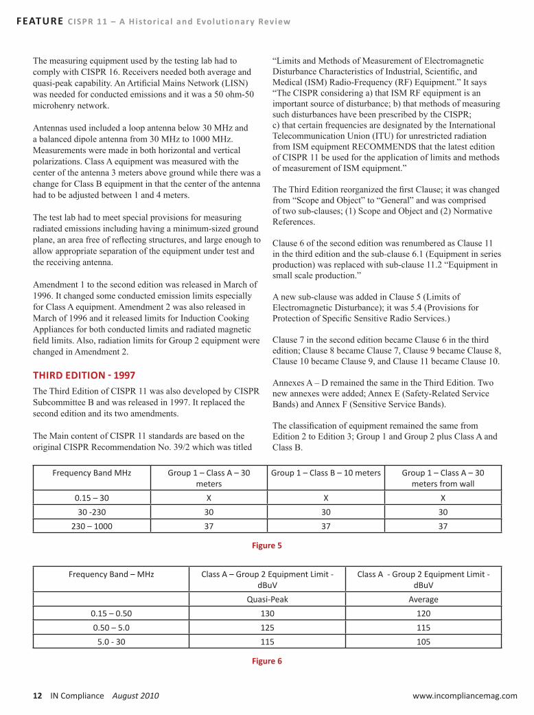
THIRD EDITION - 1997The Third Edition of CISPR 11 was also developed by CISPR Subcommittee B and was released in 1997. It replaced the second edition and its two amendments.
The Main content of CISPR 11 standards are based on the original CISPR Recommendation No. 39/2 which was titled
“Limits and Methods of Measurement of Electromagnetic Disturbance Characteristics of Industrial, Scientific, and Medical (ISM) Radio-Frequency (RF) Equipment.” It says “The CISPR considering a) that ISM RF equipment is an important source of disturbance; b) that methods of measuring such disturbances have been prescribed by the CISPR; c) that certain frequencies are designated by the International Telecommunication Union (ITU) for unrestricted radiation from ISM equipment RECOMMENDS that the latest edition of CISPR 11 be used for the application of limits and methods of measurement of ISM equipment.”
The Third Edition reorganized the first Clause; it was changed from “Scope and Object” to “General” and was comprised of two sub-clauses; (1) Scope and Object and (2) Normative References.
Clause 6 of the second edition was renumbered as Clause 11 in the third edition and the sub-clause 6.1 (Equipment in series production) was replaced with sub-clause 11.2 “Equipment in small scale production.”
A new sub-clause was added in Clause 5 (Limits of Electromagnetic Disturbance); it was 5.4 (Provisions for Protection of Specific Sensitive Radio Services.)
Clause 7 in the second edition became Clause 6 in the third edition; Clause 8 became Clause 7, Clause 9 became Clause 8, Clause 10 became Clause 9, and Clause 11 became Clause 10.
Annexes A – D remained the same in the Third Edition. Two new annexes were added; Annex E (Safety-Related Service Bands) and Annex F (Sensitive Service Bands).
The classification of equipment remained the same from Edition 2 to Edition 3; Group 1 and Group 2 plus Class A and Class B.
Frequency Band MHz Group 1 – Class A – 30 meters
Group 1 – Class B – 10 meters Group 1 – Class A – 30 meters from wall
0.15 – 30 X X X
30 -230 30 30 30
230 – 1000 37 37 37
Figure 5
Frequency Band – MHz Class A – Group 2 Equipment Limit - dBuV
Class A - Group 2 Equipment Limit - dBuV
Quasi-Peak Average
0.15 – 0.50 130 120
0.50 – 5.0 125 115
5.0 - 30 115 105
Figure 6

August 2010 IN Compliance 13
CISPR 11 – A Histor ical and Evolut ionary Review FEATURE
With respect to the Limits of electromagnetic disturbance, Class A equipment could still be tested either at a test lab or in situ while Class B equipment had to be measured in a testing laboratory.
The limits for conducted emissions on the power leads were measured from 150 kHz to 30 MHz using a 50ohm/50uH network. The limits remained the same for Class A and Class B equipment from Edition 2 except that another category was added for Class A-Group 2 equipment for mains supply currents in excess of 100 amps per phase when using the CISPR voltage probe. The limits are shown in Figure 6 for this special case.
However, new limits were added in Table 2c (Mains terminal disturbance voltage for inductive cooking appliances) for Group 2-Class B equipment for both domestic and commercial cooking appliances.
Table 3 (Electromagnetic radiation disturbance limits for group 1 equipment) had a major change as the measurement distance for Group 1-Class A equipment was changed from 30 meters to 10 meters with a corresponding increase in limits of 10 dB (assuming an inverse distance fall-off of the radiated electromagnetic field.)
Par. 5.2.2 of this edition also introduced the concept of measuring products at shorter distances than the specified measurement distances for radiated disturbances. For example, it allowed Group 2 Class A equipment to be measured at a distance of between 10 and 30 meters instead of 30 meters. Also, it allowed Group 1 and 2, Class B, equipment to be measured at antenna distances between 3 and 10 meters. However, it stated that “In case of dispute, Class A-Group 2 equipment shall be measured at a distance of 30 meters; Class B-Group 1, Class B- Group 2, and Class A-Group 1 equipment SHALL be measured at a distance of 10 meters.”
Tables 3a and 3b were added to cover Group 2 induction cooking appliances for Class B and Class A, respectively. Table 3a (Limits of the magnetic field induced current in a 2 m loop antenna around the device under test) was intended to use the “Van Veen Loop Method” measurement method as per CISPR 16-2. Table 3b (Limits of the magnetic field strength) is measured at a 3-meter antenna distance with a 0.6 meter loop antenna as described in CISPR 16-1.
Table 4 (Electromagnetic radiation disturbance limits for Group 2 – Class B equipment measured on a test site) added a new column of requirements which was simply: the quasi-peak magnetic field (measured at 3 meters) will not exceed 39 dBuA/meter decreasing linearly with the logarithm of the frequency to 3 dBuA/meter from 150 kHz to 30 MHz.
14 IN Compliance August 2010 www.incompliancemag.com
FEATURE CISPR 11 – A Histor ical and Evolut ionary Review
Table 5 changed the measurement distance from 30 meters to 10 meters and increased the limits by 10 dB from Edition 2 limits.
Table 6 was added to the Third Edition. It was titled “Electromagnetic radiation disturbance peak limits for Group 2- Class B ISM equipment producing CW-type disturbances and operating at frequencies above 400 MHz.” Table 7 (Electromagnetic radiation disturbance peak limits for Group 2- Class B ISM equipment producing fluctuating disturbances other than CW and operating at frequencies above 400 MHz) and Table 8 (Electromagnetic radiation disturbance weighted limits for Group 2 – Class B ISM equipment operating at frequencies above 400 MHz) were also added to the Third Edition.
Clause 5.4 (Provisions for protection of specific sensitive radio services) was added to the fourth edition and it referenced the new Annex F which gave examples of bands to be protected.
The same general measurement conditions existed as in the previous edition which is that Class A equipment could be measured at a test lab or in situ. Class B equipment had to be measured on a test site (in a test lab).
For equipment on a turntable, the distance to the antenna was measured from the center of the turntable. For equipment not on a turntable, the distance to the antenna was measured from the edge of the equipment.
Paragraph 6.5.6 (Single and multiple-zone induction cooking appliances) was added to the third edition.
Amendment 1 to the Third Edition added requirements for ISM lighting apparatus operating in the frequency bands of 915 MHz, 2.45 GHz, and 5.8 GHz. It also added IEC 60705:1999 (Household microwave ovens – methods for measuring performance) to the normative standards. It also added new words in Clause 5.2.2 (discussed earlier) and it added Table 5 (Electromagnetic Radiation disturbance limits for Group 2 – Class A equipment). All new wording was added to Clause 5.2.3 by Amendment 1. In Clause 6.2.1, it added the requirement that “for measurements at frequencies above 1 GHz, a spectrum analyzer with characteristics as defined in CISPR 16-1 shall be used.” Additionally, in clause 6.2.4, it added the words “for measurements at frequencies above 1 GHz, the antenna used shall be as specified in CISPR 16-1.” Also, Clause 6.5.4 (Microwave cooking appliances) was added by Amendment 1. An important (and somewhat controversial) sub-clause was added by Amendment 1 in 7.1.3 (Radiation measurements [9 kHz to 1 GHz]). It added two sentences that impacted Edition 3 and future editions. The first sentence said “For the test site measurements, an
inverse proportionality factor of 20 dB per decade shall be used to normalize the measured data to the specified distance for determining compliance.” Also, it added the parenthetical sentence, “Care should be taken in measuring a large test unit at 3 meters at a frequency near 30 MHz due to near-field effects.” It deleted a key sentence from Edition 2 that said “At the closer measurement distance the electromagnetic disturbances measured shall not exceed the limit values specified in Clause 5.” In sub-clause 8.2 it added the sentence “The distance between the receiving antenna and the EUT shall be 3 meters.” Sub-clauses 8.3 (Validation and calibration of test site) and 8.4 (Measuring Procedure) were completely rewritten. Finally, Amendment 1 added Figure 5 (Decision tree for the measurement of emissions from 1 GHz to 18 GHz of Class B- Group 2 ISM equipment operating at frequencies above 400 MHz).
Amendment 2 replaced “spark erosion equipment” with “electro-discharge machining (EDM) and arc welding equipment.” It also made additional editing changes to a number of sub-clauses.
FOURTH EDITION - 2003The Fourth Edition of CISPR 11 was published in March of 2003. The Fourth Edition superseded the Third Edition (1997), its first amendment (1999) and its second amendment (2002).
There were a limited number of changes in going from the Third Edition to the Fourth Edition. The first two sentences in Clause 4 were changed to read “The manufacturer and/or supplier of ISM equipment shall ensure that the user is informed about the class and group of the equipment, either by labeling or by the accompanying documentation. In both cases, the manufacturer/supplier shall explain the meaning of both the class and the group in the documentation accompanying the equipment.”
Clauses 7.1 and 7.2 were interchanged from the Third Edition.
Clause 6.2.5 (Artificial Hand) was added in Edition 4 as well as Figure 6 (Artificial Hand, RC Element). The concept of an artificial hand was introduced to simulate the effects of the user’s hand during the conducted emission measurements
The definitions of Group 1 ISM equipment, Group 2 ISM equipment, Class A equipment, and Class B equipment remained basically the same as the Third Edition.
With respect to limits of electromagnetic disturbance, Class A equipment could, again, be measured either in a testing laboratory or in situ (as preferred by the manufacturer). However, again, Class B equipment must be measured in a testing laboratory.


16 IN Compliance August 2010 www.incompliancemag.com
FEATURE CISPR 11 – A Histor ical and Evolut ionary Review
The limits of terminal disturbance voltage (conducted emissions) gives the manufacturer two choices: (1) meet the average limit with an average detector and the quasi-peak limit with a QP detector or (2) meet the average limit when using a QP detector. This was the same as stated in Edition Three.
For radiated disturbances from 150 kHz to 1000 MHz, the limits stayed basically the same as the third edition. Measurements were allowed at closer distances than the specified distances, under certain considerations. In case of dispute, however, Class B (Group 1 and Group 2) and Class A (Group 1) shall be measured at a distance of 10 meters and
Class A (Group 2) shall be measured at a distance of 30 meters.
Receivers use for the measurements shall meet the criteria of CISPR 16-1. The artificial mains network (LISN) remained the same as the third edition; a 50 ohm/50 microhenry V-Network as specified in CISPR 16-1. The antennas used for measuring CISPR 11 products must meet CISPR 16-1. In a testing laboratory, the antenna must be raised and lowered from 1 to 4 meters in the frequency range 30 MHz to 1000 MHz. For measuring products in situ, the antenna’s center must be fixed at 2 meters above the ground.
CISPR 11 – Edition 1 – 1975 CISPR 11 – Edition 5 - 2009
Foreword Foreword
Preface Introduction
1 – Scope 1- Scope
2 – Object 2 – Normative References
3 – Definitions 3 – Terms and Definitions
4 – Limits of Interference 4 – Frequencies Designated for ISM Use
5 – Methods of Measurement 5 – Classification of ISM Equipment
6 – Safety Precautions 6 – Limits of Electromagnetic Disturbance
Appendix A – Precautions to be taken in the use of a Spectrum Analyzer
7 – Measurement Requirements
Appendix B – Propagation of Interference from industrial RF equipment at frequencies between 30 MHz and 300 MHz
8 – Special Provisions for Test Site Measurements (9 kHz to 1 GHz)
Appendix C – Artificial Mains Networks for currents between 25 amps and 100 amps
9 – Radiation Measurements – 1-18 GHz
10 – Measurements in situ
11 – Safety Precautions
12 – Assessment of Conformity of Equipment
13 – Figures and Flowcharts
Annex A (Informative) – Examples of Equipment Classification
Annex B (Informative) – Precautions to be taken in the use of a Spectrum Analyzer (see 6.3.1)
Annex C (Normative) – Measurement of Electromagnetic Radiation disturbances in the presence of signals from radio transmitters
Annex D (Informative) – Propagation of Interference from industrial radio frequency equipment at frequencies between 30 MHz and 300 MHz
Annex E (Informative) – Recommendations of CISPR for protection of certain radio services in particular areas
Annex F (Informative) –Frequency Bands allocated for safety-related radio services
Annex G (Informative) – Frequency Bands allocated for sensitive radio services
Bibliography
FIgure 7
August 2010 IN Compliance 17
CISPR 11 – A Histor ical and Evolut ionary Review FEATURE
Amendment 1 to Edition 4 was released in 2004; it primarily replaced Table 6 in Edition 4 with a new table that addresses Group 2 (Class A and Class B) ISM equipment producing CW type disturbances and operating at frequencies above 400 MHz.
Amendment 2 added CISPR 16-4-2:2003 to the Normative References. It also added a new Table 2c for Mains Terminal disturbance voltage for induction cooking appliances. It also modified Clause 6.5.4 (Microwave Cooking Appliances) and 6.5.6 (Single and multiple-zone induction cooking appliances) to more closely match the IEC Product Standard. Amendment 2 also added clauses 6.6 (Recording of test-site measurement results), 6.6.1 (Conducted Emissions), and 6.6.2 (Radiated Emissions). Also, Clause 11.4 (Measurement Uncertainty) was added and it said “Determining compliance with the limits in this standard shall be based on the results of the compliance measurement, not taking into account measurement instrumentation uncertainty.” However, results of measurements of emissions from ISM equipment were supposed to reference the measurement uncertainty considerations contained in CISPR 16-4-2.
FIFTH EDITION - 2009The Fifth Edition of CISPR 11. the current edition, was released in 2009.
The Fifth Edition continued the long-standing practice of Group 1 and Group 2, Class A and Class B equipment classifications. The limits stated in the 2009 edition were similar to the limits in the Fourth Edition.
A comparison of the table of contents of the First Edition and the Fifth Edition indicates the growth in length and complexity of the standard over a period of 35 years (Figure 7).
Edition 5’s first Clause is titled “Scope” versus the previous Edition’s title of “General.” Clause 2 has a new title; “Normative References.” Clause 3 (Terms and Definitions) is also new. Clause 4 (Frequencies Designated for ISM Use) was the previous Ediiton’s Clause 3. Clause 5 was the same as Edition 4’s Clause 4 except Edition 5 added sub-clause 5.1 (Information for the user) to the main body of the standard.
Clause 6 underwent a major overhaul from Edition 4. Its Main Clause and Sub-Clause headings are as follows:Clause 6 – Limits of Electromagnetic Disturbance 6.1 – General 6.2 – Group 1 Measured on a Test Site 6.3 – Group 2 Measured on a Test Site 6.4 – Group 1 and Group 2 Class A Measured in situ
Clause 7 added a new sub-clause 7.1 (General) and a new sub-clause 7.7 (Recording of Test Site Measurement Results).
Clause 12 (Assessment of Conformity of Equipment) added a new sub-clause 12.1 (General) and then the next three sub-clauses were the same as sub-clauses 11.1 – 11.3 in Edition 4.
Clause 13 is new and titled “Figures and Flowcharts.” Annex E is also new for Edition 5.
The entire Edition was written to have a more transparent structure.
Table 17 was added with a title of “Electromagnetic Radiation Disturbance Limits for Class A Group 1 Equipment Measured in situ.” It especially addressed equipment with input power greater than 20 KVA.
An Amendment 1 to Edition 5 was released in 2010. It created a new subset of equipment, Small Equipment. Small Equipment was defined to be “equipment, either positioned on a table top or standing on the floor which, including its cables, fits in a cylindrical test volume of 1.2 meters in diameter and 1.5 meters above the ground plane.”
Using this definition, Tables 4, 5, 9, 10, and 11 were modified to allow testing of Class A and B products meeting the “Small Equipment” definition to be tested at a 3-meter test distance. The limit at three meters would be extrapolated from the typical test distance of 10 meters using an inverse-distance fall-off assumption (free-field).
SUMMARY AND CONCLUSIONSThe CISPR 11 standard for measuring disturbances (emissions) from Industrial, Scientific, and Medical Equipment has been in existence for over 35 years. It has grown from a simple document to a complex document involving a number of types of products.
It has grown from measuring products at a larger distance (100 meters and 30 meters) for Class A Equipment to measuring them at 3 meters. Class B equipment measurement distances have seen an equivalent degradation of “far-field” radiated emission measurements. This steady erosion of the “laws of physics” is worrisome and a trend to reverse this erosion is overdue in the engineering field of EMC and the EMC Standards arena. n
Dan Hoolihan is the president of Hoolihan EMC Consulting and can be reached by e-mail at [email protected].
by Chris Burket, TDK Corporation
Understanding the Importance of Ferrite Bead Material Behavior

August 2010 IN Compliance 19
A common scenario: A design engineer inserts a ferrite bead into a circuit experiencing EMC problems, only to find that the bead has actually caused the unwanted
to noise to be WORSE. How can this be? Aren’t ferrite beads supposed to remove noise energy and not make the problem worse?
The answer to this question is fairly simple, but may not be widely understood outside of those who work a majority of their time solving EMI issues. Simply put, a ferrite bead is not a ferrite bead is not a ferrite bead, etc. Most ferrite bead manufacturers provide a table which lists their part number, the impedance at some given frequency (usually 100 MHz), the DC resistance (DCR), a maximum current rating and some dimensional information (see Table 1). All pretty much standard stuff. What is not shown in the data table is material information and the respective performance characteristics over frequency.
WHAT IS A FERRITE BEAD?A ferrite bead is a passive device that removes noise energy from a circuit in the form of heat. The bead creates impedance over a broad frequency range that eliminates all or part of the undesired noise energy over that frequency range. For DC voltage applications (such as Vcc lines for ICs), it is desirable to have a low DC resistance value as to not have large power losses within the desired signal and/or voltage or current source (I2 x DCR losses). However, it is desirable to have high impedance over some defined frequency range. Therefore, the impedance is related to the material used (permeability), the size of the ferrite bead, the number of windings and the winding construction. Obviously, the more windings within a given case size and for a specific material used, the higher the impedance, but this will also yield higher DC resistance as the physical length of the inner coil is longer. The part’s rated current is inversely proportional to its DC resistance.
One of the fundamental aspects of using ferrite beads for EMI applications is that the component must be in its resistive stage. What does this mean? Simply, it means that
Table 1: Typical Ferrite Bead Data Table

20 IN Compliance August 2010 www.incompliancemag.com
FEATURE Al l Ferr i te Beads Are Not Created Equal
“R” (AC resistance) must be greater than “XL” (inductive reactance). At frequencies where XL > R (lower frequencies), the part behaves more as an inductor than a resistor. At frequencies where R > XL, the part behaves as a resistor which is the desired property of the ferrite bead. The frequency, at which “R” becomes greater than “XL,” is called the “cross-over” frequency. This is shown in Figure 1 with the cross-over frequency marked, 30 MHz in this example, by the red arrow.
Another way to look at this is in terms of what the part is actually doing while in its inductive and resistive stages. Like other applications where there is an impedance mismatch with inductors, part of the introduced signal is reflected back to the source. This can provide some protection for sensitive devices on the other side of the ferrite bead, but also introduces an
“L” into the circuitry and this can cause resonances and oscillations (ringing). So when the bead is still inductive in nature, part of the noise energy will be reflected and some percentage will pass through, depending on the inductance and impedance values.
When the ferrite bead is in its resistive stage, the component behaves, as stated, like a resistor and therefore impedes the noise energy and absorbs this energy from the circuit and does so in the form of heat. Though constructed in an identical manner as some inductors, using the same processes, manufacturing lines and techniques, machinery and some of the same component materials, the ferrite bead uses a lossy ferrite material while an inductor utilizes a lower loss ferrite material. This is shown in curves of Figure 2.
Figure 1: Cross Over Frequency
Figure 2: Reflection vs. Absorption
Figure 3: 120 Ohm (at 100 MHz) Ferrite Beads
Figure 4: Typical Impedance Curve with /Z/, R, XL
August 2010 IN Compliance 21
Al l Ferr i te Beads Are Not Created Equal FEATURE
This figure shows [μ’’] which is used to reflect the behavior of the lossy ferrite bead material.
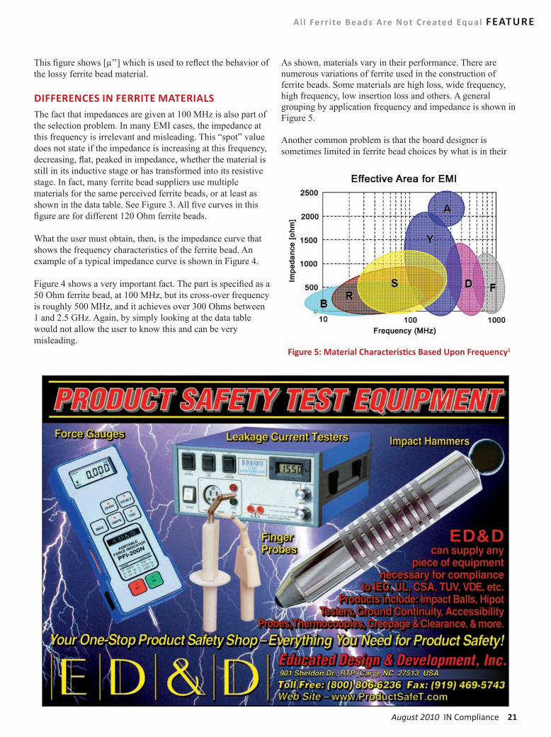
DIFFERENCES IN FERRITE MATERIALSThe fact that impedances are given at 100 MHz is also part of the selection problem. In many EMI cases, the impedance at this frequency is irrelevant and misleading. This “spot” value does not state if the impedance is increasing at this frequency, decreasing, flat, peaked in impedance, whether the material is still in its inductive stage or has transformed into its resistive stage. In fact, many ferrite bead suppliers use multiple materials for the same perceived ferrite beads, or at least as shown in the data table. See Figure 3. All five curves in this figure are for different 120 Ohm ferrite beads.
What the user must obtain, then, is the impedance curve that shows the frequency characteristics of the ferrite bead. An example of a typical impedance curve is shown in Figure 4.
Figure 4 shows a very important fact. The part is specified as a 50 Ohm ferrite bead, at 100 MHz, but its cross-over frequency is roughly 500 MHz, and it achieves over 300 Ohms between 1 and 2.5 GHz. Again, by simply looking at the data table would not allow the user to know this and can be very misleading.
As shown, materials vary in their performance. There are numerous variations of ferrite used in the construction of ferrite beads. Some materials are high loss, wide frequency, high frequency, low insertion loss and others. A general grouping by application frequency and impedance is shown in Figure 5.
Another common problem is that the board designer is sometimes limited in ferrite bead choices by what is in their
Figure 5: Material Characteristics Based Upon Frequency1
22 IN Compliance August 2010 www.incompliancemag.com
FEATURE Al l Ferr i te Beads Are Not Created Equal
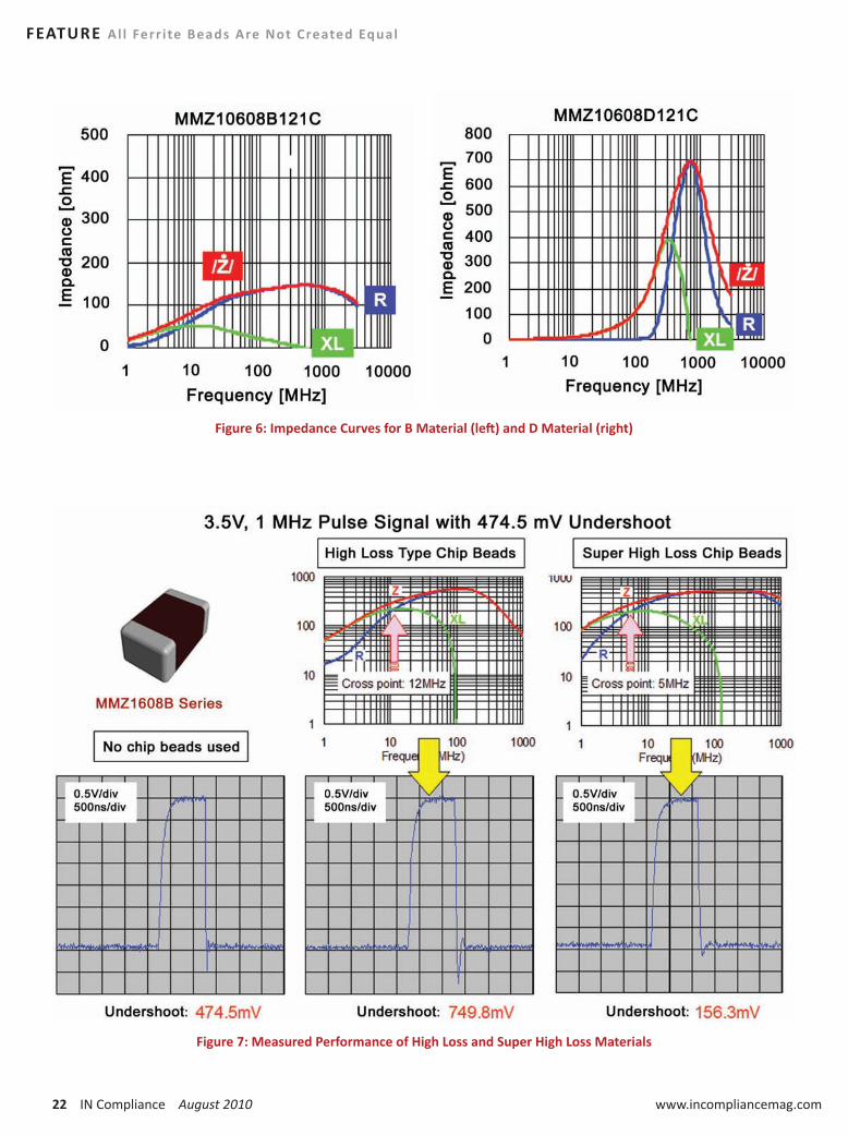
Figure 6: Impedance Curves for B Material (left) and D Material (right)
Figure 7: Measured Performance of High Loss and Super High Loss Materials
August 2010 IN Compliance 23
Al l Ferr i te Beads Are Not Created Equal FEATURE
approved component database. If the company has only a few approved ferrite beads which have been used on other products and were deemed satisfactory, in many cases there is no perceived need to evaluate and approve other materials and part numbers. This has many times, in the recent past, led to some of the worsening effects of the original EMI noise problem mentioned above. What worked before may or may not work on the next project. One can’t simply carry over the last project’s EMI solution, especially if the frequency has changed for the desired signal or there are frequency changes in potentially radiating components such as clock devices.
COMPARING CROSS-OVER FREQUENCIESIf one takes a look at the two impedance curves in Figure 6, a comparison can be made of the material effects of two similar specified parts.
For both parts, the impedance at 100 MHz is 120 Ohms. For the part on the left, using the “B” material, the maximum impedance is around 150 ohms and is achieved at 400 MHz. For the part on the right, using the “D” material, the maximum impedance is 700 Ohms as is achieved at approximately 700 MHz. But the biggest difference is in the cross-over frequencies. The super high loss “B” material transitions (R > XL) at 6 MHz while the very high frequency “D” material remains inductive until around 400 MHz. Which is the right part to use? It depends on each individual application.
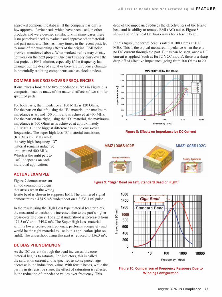
ACTUAL EXAMPLEFigure 7 demonstrates an all too common problem that arises when the wrong ferrite bead is chosen to suppress EMI. The unfiltered signal demonstrates a 474.5 mV undershoot on a 3.5V, 1 uS pulse.
In the result using the High Loss type material (center plot), the measured undershoot is increased due to the part’s higher cross-over frequency. The signal undershoot is increased from 474.5 mV up to 749.8 mV. The Super High Loss material, with its lower cross-over frequency, performs adequately and would be the right material to use in this application (plot on right). The undershoot using this part is reduced to 156.3 mV.
DC BIAS PHENOMENONAs the DC current through the bead increases, the core material begins to saturate. For inductors, this is called the saturation current and is specified as some percentage decrease in the inductance value. With ferrite beads, while the part is in its resistive stage, the effect of saturation is reflected in the reduction of impedance values over frequency. This
drop of the impedance reduces the effectiveness of the ferrite bead and its ability to remove EMI (AC) noise. Figure 8 shows a set of typical DC bias curves for a ferrite bead.
In this figure, the ferrite bead is rated at 100 Ohms at 100 MHz. This is the typical measured impedance when there is no DC current through the part. But as can be seen, once a DC current is applied (such as for IC VCC inputs), there is a sharp drop-off of effective impedance, going from 100 Ohms to 20
Figure 8: Effects on Impedance by DC Current
Figure 9: “Giga” Bead on Left, Standard Bead on Right2
Figure 10: Comparison of Frequency Response Due to Winding Configuration

24 IN Compliance August 2010 www.incompliancemag.com
FEATURE Al l Ferr i te Beads Are Not Created Equal
Ohms in the above curves for just a 1.0 A current at 100 MHz. Maybe not too critical, but something the design engineer must be aware of. Again, by using only the parts’ electrical characteristic data from the supplier’s datasheet, the user would have no knowledge of this DC bias phenomenon.
FREQUENCY RESPONSE VS. WINDING CONSTRUCTIONAs with high frequency RF inductors, the winding direction of the inner coils within the ferrite bead has a large impact on the frequency behavior of the bead. The winding direction
influences not only the impedance versus frequency levels, but also shifts the frequency response. In Figure 9, two 1000 Ohm ferrite beads, in the same case size and made of the same material but with two different winding configurations, are shown.
The part on the left, with coils wound in the vertical plane and stacked in the horizontal direction, yields higher impedance and a higher frequency response than the part on the right which is wound in the horizontal plane and stacked in the vertical direction. This is, in part, due to the lower capacitive reactance (XC) associated with the reduced parasitic capacitance between the end terminations and the inner coils. The lower XC creates a higher self resonance frequency which then allows the ferrite bead to continue to increase in impedance up to the higher self resonance frequency, resulting also in a higher obtainable impedance value than possible with a standard constructed ferrite bead. The curves for the above two 1000 Ohm ferrite beads are shown in Figure 10.
ACTUAL TEST RESULTSTo further show the impact of correct and incorrect ferrite bead selection, a simple test circuit and test board were used to demonstrate much of what has been discussed above. In Figure 11, a test board is shown with three ferrite bead locations and test points labeled as “A”, “B”, and “C” at 0 mm, 50 mm, and 100 mm distance from the output of the transmitting (TX) device, respectively.
Signal conditions for this test were the following:
Frequency: 8 MHzDuty Cycle: 50%High voltage: 5VLow voltage: 0V Rise time: 1.6 nSFall time: 1.8 nS
The signal integrity was measured on the output side of the ferrite bead at each of the three locations and duplicated with two ferrite beads made of different materials. The first material, a low frequency, lossy “S” material was tested at points “A,” “B” and “C”. Next, a higher frequency “D” material was used. The point to point results using these two ferrite beads are shown in Figure 12.
Figure 11: Test Setup and Test Board
Figure 12: In-Circuit Performance Testing Results


26 IN Compliance August 2010 www.incompliancemag.com
FEATURE Al l Ferr i te Beads Are Not Created Equal
The “through” unfiltered signal is shown in the center row and exhibits some overshoot and undershoot on the rising and falling edges respectively. As can be seen, with the use of the correct material for the above test conditions, the lower frequency, lossy material exhibited good overshoot and undershoot signal improvement on the rising and falling edges. These results are shown in Figure 12 in the upper row. The results using the high frequency material caused ringing that magnified the levels of each and increased the period of instability. These test results are shown in the bottom row.
When looking at the improvement on EMI over frequency for the recommended upper part (in Figure 12) in the horizontal scan shown in Figure 13, it can be seen that this part substantially reduces the EMI spikes and reduces the overall noise levels, for all frequencies in the 30 to approximately 350 MHz range, to an acceptable level well below the EMI limit highlighted by the red line, which is the general regulatory standard for Class B devices (FCC part 15 in the US). The “S” material used in the ferrite bead is specifically for these lower frequencies. And as can be seen, the “S” material has limited impact on the original, unfiltered EMI noise levels once the frequency gets above 350 MHz, but does reduce the one major spike at 750 MHz around 6 dB. If the major portion of the EMI noise problem was above 350 MHz, one would need to look at using a higher frequency ferrite material that has its impedance maximum higher in the frequency spectrum.
Of course all of the ringing, shown in the bottom curves in Figure 12, is typically avoided by actual performance testing and/or simulation software, but it is hoped that this article will allow the reader to bypass a lot of the common errors, decrease the amount of time needed to select the correct
ferrite bead and allow for a more “educated” starting point when a ferrite bead is needed to help solve an EMI issue.
CONCLUSIONTo avoid misuse in your future ferrite bead needs, it is recommended that you always:
1. Understand the noise problem within your circuit, including noise sources
2. Choose the correct material behavior needed, e.g., high loss at low frequencies
3. Determine the allowable trade-off for DC resistance and needed AC impedance
4. Get the impedance curve and other data for the part to be used
5. Don’t automatically use what has worked before
6. Don’t assume that a ferrite bead will be the best EMI component to use
7. If in doubt, contact your ferrite bead supplier as they will have EMI experts
In closing, it is desirable to approve families or series of ferrite beads, not just individual part numbers, to have more options and design flexibility. It needs to be noted that different suppliers use different materials, and it is a must that the frequency performance of each be reviewed, especially when doing multiple sourcing for the same project. This is somewhat easy to do on a first time basis, but once parts are entered into a component database under one control number, and they can be used anywhere thereafter, it is important that the frequency performance of the different suppliers’ parts closely resemble each other in order to eliminate potential future problems for other applications. The best way to do this is to have similar data from the various suppliers and, as a minimum, have the impedance curve. This will also ensure the right ferrite bead is being used to solve your EMI problem.
And remember, not all ferrite beads are created equal. n
NOTES1. Material designations “B,” “R,” “S,” “Y,” “A,” “D” and “F”
are those of the author’s company only and reflect different frequency behavior. Other ferrite bead suppliers have their own material designations.
2. “Giga” is a product name of the author’s company only.
Chris Burket has been with TDK since 1995 and is now a senior applications engineer supporting a vast array of passive components. He has been involved in product design, technical sales and marketing. Mr Burket has written and presented technical papers at numerous forums. Mr. Burket had been awarded three U.S. patents in optical/mechanical switches and in capacitors. Mr. Burket can be reached at [email protected] 13: Radiated EMI Noise (Horizontal) Suppression


28 IN Compliance August 2010 www.incompliancemag.com
Lack of Global StandardizationDirectly Impacts Market Access
A great number of companies define themselves as global, yet their scope for “global” varies and therefore so does their global compliance needs. One
company might market its products in the U.S., Canada and European Union, while another might be introducing new products to 150-plus countries. No matter the company’s definition of “global,” there are several critical areas they should address to ensure they are truly ready to place products on markets worldwide.
Most companies will have some standard development process that deals with the product lifecycle – from new product conception through the end of the product’s life cycle. This article deals with new product conception through
market introduction phases, as well as the compliance staff’s specific contributions.
NEW PRODUCT CONCEPTIONNormally, at this stage of development, only the basic product functions are identified, including the product features, revenue opportunities and market opportunities (where and when the product needs to be introduced). This is the key stage in the standard development process. The chances of a successful project are increased significantly if:
y Opportunities have been identified at the country level, and
y The right team members have evaluated the product opportunity.
by Bill Holz, TÜV Rheinland of North America
Bring Your Regulatory Compliance Staff into the Process Early to Achieve Success


30 IN Compliance August 2010 www.incompliancemag.com
FEATURE Lack of Global Standardizat ion Direct ly Impacts Market Access
This is probably the most common shortcoming for many companies – where the product opportunity is developed and evaluated by a single organization or does not include all the key organizations. Companies must properly address a new opportunity by involving all of the key staff members from:
y Marketing
y R&D (Engineering)
y Regulatory Compliance
y Finance
The involvement of these organizations will ensure that all key aspects pertaining to a successful product development and launch will be addressed. The role the regulatory compliance staff plays during this phase is considerable. Many times these contributions are overlooked until it is too late in the game to overcome an incorrect product introduction assumption. This is especially true with respect to each country’s regulatory and technical requirements.
COUNTRY REGULATORY AND TECHNICAL REQUIREMENTSFrom this point, we can assume that the product conception document lists each country (where the product introduction will occur), the product launch date and the anticipated revenue. The compliance staff should then be able to provide information on the following:
y Regulated Products. Depending on the product, certain certifications must be obtained before a product can be legally placed on a specific country’s market. Some products may not have any requirements, while others need a variety of certifications such as:
{ Product safety
{ EMC
{ Energy
{ Telecom/radio
{ Medical
The ramifications of not knowing, or knowing yet not complying, are significant. Not every country is set up to maintain high surveillance on mandatory certifications, but the risk remains if compliance is not met with legal regulations and fines, and in some cases worse can be imposed.
y Technical Requirements. Is the envisioned product designed to meet the technical requirements for each country on the list? Have you identified a technology that may only be acceptable to certain countries?
This situation is quite common. A company takes a product – designed for North American standards – and wants to place it on global markets. The problem is not so much that one fails to gain regulatory certifications, but rather, it is often not possible to even use these products in other global markets.
y Testing Requirements. Depending on the product and country, there may be specific requirements as to where the testing must be performed or which test reports will be accepted in lieu of in-country testing. In countries where the product is regulated, it is necessary to either perform in-country testing or submit test reports to the correct standard from an accredited lab.
This is a cost concern. First, know the number of samples required for testing in each country. Second, learn which existing test reports will be accepted in which countries. In most cases, accepted test reports come from an accredited laboratory.
In addition, the U.S. has a Mutual Recognition Agreement (MRA) with several countries regarding test reports. The contracted laboratories must be accredited for the appropriate standards, and maximum coverage under available MRA’s must be obtained.
y Language Requirements. To submit a product for mandatory certifications, each authority must dictate the language of the application and user documentation to be accepted.
This is a cost concern. It only makes sense that a product placed in a foreign country must have user documentation written in the intended users’ language. In many cases, it is required that the application and user documents be in the prescribed language for the application to be submitted. In others, it can be submitted in English to gain the certification, but must also be in the local language prior to placing on the market. Still, others will allow everything to be in English. Translation is expensive and can further delay certifications if it is incomplete.
y Local Residence Requirements. Each authority has requirements regarding the applicants’ legal establishment (residence). In many cases, the formal application must be signed by a legal entity located within that country. These requirements, and how to fulfill them, varies considerably.
This is a cost concern. In many cases, the legal applicant must be an established resident of the country where the application is being made. An established resident can be a locally based company, distributor or licensed agent. Not knowing these legal requirements can cause serious delays,
August 2010 IN Compliance 31
Lack of Global Standardizat ion Direct ly Impacts Market Access FEATURE
and significant costs can be incurred if the company does not have a legal solution.
y Lead Time for Certification. How long it takes to attain certification is not only dependent on each country’s process, but also the time of year the product introduction is planned. Holidays and heavy vacation periods must be taken into account.
This is a cost concern. Revenue planning for a given country should assume that all required certifications have been attained. It is not a simple case of estimating the time (usually overly optimistic) but rather the actual time for these efforts. The same product can take 2 weeks in one country and 12 weeks in another. To properly plan revenue, companies need to know the actual timeline.
y Documentation Requirements. To submit an application in any country, you must provide specific product and company information. The application process will not start until all documentation has been made available.
This is a cost concern primarily from the perspective of delayed revenue. An application can be submitted to an authority without all required documents, but the application will not be processed. Even worse, many incomplete applications are just set to the side and lost.
The time to gain a certification, as discussed above, is based on a start date when all samples and/or required documents are available. Providing anything less will not start the clock for the approval. All requested documents must be provided.
If submitting these highly technical documents is not a concern and if one does not or cannot provide them, then no certifications will be granted. Therefore, if information cannot be provided to specific countries, then those markets should be removed from the list.
y Cost for Certifications. Once again, the cost to attain a certification will vary significantly from country to country.
There is no way to avoid the cost required to pay for certifications, but it is important to know the cost associated with each country. There may be many cases where the certification cost for a particular country may far outweigh the potential revenue margins. It is better to cross off these revenue-loss situations before investing in the process and know the full cost beforehand.
There is another aspect regarding the cost of certifications: the loss of revenue due to certification delays. This is a far bigger number than actual certification costs. Just consider
that there is only a maximum of 260 selling days per year (actually less). Any lost planned revenue days cannot be recovered; they are gone. This can be figured out quite easily. Divide that country’s annual planned revenue by 260 days to calculate the revenue per day. For example, planned revenue of $2.6 million can be estimated at $10,000 per day revenue. The daily loss typically is considerably higher than certification costs. This is where a good partner in global certifications will end up making money by getting products certified on time.
SUMMARYUnlike the European Union, there is very little, if any, standardization of any of the above items or process harmonization for the rest of the world. Therefore, the compliance staff will need to investigate each of the above aspects for each country on the list. The dynamics are such that the regulations vary considerably from country to country, but they also change frequently. Old information cannot be reused; the task must be done frequently.
Each one of the listed items has a direct impact on a company’s ability to develop the correct product as well as legally place it on the market. For each item, there is also a cost impact – not only direct costs, but costs associated with:
y Time to place it on the market
y Lost revenue from improperly planned certification time
y Time for planned market introduction
Far too often regulatory compliance staff members are brought into the picture too late in the new product conception phase. As a result, products may be improperly defined to meet the intended market, or applicable regulations and associated costs may not be taken into account – resulting in less then acceptable profitability for the product. The issues presented seem to be amplified in today’s economy, but no matter what the economic situation, use the compliance staff to the fullest to bring products to a successful and profitable launch. n
Bill Holz, Senior Specialist at TÜVRheinland’s International Approvals Division since 2008, has 25 years of experience in international regulatory services. Holz is considered one of the foremost experts on the rules and pitfalls of navigating complex international regulatory procedures. He moderates the company’s popular roundtable series, “Global Regulatory Approval of Products.”

Simulating Small Device CDMUsing Spice
by Robert Ashton, ON Semiconductor,Marty Johnson, National Semiconductor Corporation
and Scott Ward, Texas Instruments

August 2010 IN Compliance 33
S imulat ing Smal l Device CDM Using Spice FEATURE
In earlier articles in this publication we have discussed the charged device model (CDM) testing of small devices. In the first article we demonstrated that the peak current
for small devices does not become vanishingly small.1 The commonly held belief of vanishing current for small devices was shown to be an artifact of measuring the current with the 1 GHz oscilloscope2 specified in the JEDEC CDM standard.6 The second article explained various ways to make CDM testing of small devices more reliable with the use of small surrogate packages, or the use of templates to hold the device during testing.3 In this article we will show how insight can be gained into the CDM testing of small devices using a simple three capacitor circuit model.4, 5
THE CDM TESTA diagram of a CDM tester built to the JEDEC field induced CDM standard6 is shown in Figure 1. The tester consists of a Field Plate, whose potential can be controlled by a high voltage power supply through a high value resistor. Above the Field Plate is a Ground Plane. At the center of the Ground Plane is a pogo pin. The pogo pin is connected to the Field Plate with a disk shaped 1 W resistor as well as to an oscilloscope through a 50 W cable. The Ground Plane can move in three dimensions relative to the Field Plate such that the pogo pin can be made to contact the pins of an integrated circuit placed pins up on the Field Plate. To perform the test, the device under test (DUT) is placed on top of a thin insulator on the Field Plate. The potential of the Field Plate is then slowly raised to a high voltage, 500 V for example. Since the capacitance between the DUT and the Field Plate is much larger than the capacitance to anything else, the DUT potential will closely track the Field Plate potential. To perform the actual stress the Ground Plane is moved such that the pogo pin touches a pin of the DUT. This quickly grounds the DUT, resulting in a very fast current pulse between the DUT and the pogo pin. The oscilloscope measures the CDM current pulse by sensing the voltage across the 1 W resistor. Sample CDM waveforms are shown in Figure 2 for the small and large modules specified in the JEDEC CDM standard to calibrate CDM testers. These modules consist of small metal coins of a specified size and capacitance to the Field Plate.
CIRCUIT MODELThe above explanation of how a field induced CDM test is performed does not
show what controls the magnitude and time dependence of a CDM event. To do this a circuit model is useful and a simple one is shown in Figure 3. CDUT is the capacitance between the DUT and the Field Plate, CDG is the capacitance between the DUT and the Ground Plane and CFG is the capacitance between the Field Plate and the Ground Plane. The resistance between the pogo pin and the Ground Plane is the 1 W current sensor. The 50 W resistance of the oscilloscope is ignored. The resistance of the spark which forms between the pogo pin and
Figure 1: Diagram of a field induced CDM tester according to the JEDEC CDM standard

34 IN Compliance August 2010 www.incompliancemag.com
FEATURE Simulat ing Smal l Device CDM Using Spice
the DUT is assumed to be a simple resistor. The inductance of the pogo pin and spark are lumped as a single inductor. The values of the spark resistance and the inductance will be used as fitting parameters. This model is the same as that proposed by Montoya and Maloney4 and the 3 capacitor model of
Atwood et al.5 Atwood has also proposed a 5 capacitor model, which includes capacitance between the Field Plate and Ground Plane to the CDM tester’s chassis, which is more accurate, especially for large size DUTs and long times. For small devices and short times the 3 capacitor model is very informative as we shall see.
The circuit in Figure 3 was implemented in the Spice simulator LTSpice7. The Spice circuit diagram, with values used to simulate the large JEDEC calibration module, is shown in Figure 4. A voltage controlled switch is used to represent the spark as the pogo pin approaches the DUT pin. A switch resistance of 26 ohms represents the resistance of
Figure 2: Measurements of the small and large JEDEC calibration modules using an 8 GHz oscilloscope
Figure 3: CDM setup with superimposed circuit diagram
Figure 4: Spice implementation of 3 capacitor CDM model
Parameter Large JEDEC Small JEDEC
Diameter (mm) 25.4 8.89
DUT to Field C 55.3 pF 6.78 pF
DUT to Ground C 1.5 pF 0.183 pF
Field to Ground C 16.1 pF 17.0 pF
Table 1: Values used in simulations
Figure 5: Comparison of measured and simulated waveforms for the JEDEC calibration modules
Figure 6: Current and voltages for a simulation of a CDM event for the large JEDEC module
August 2010 IN Compliance 35
S imulat ing Smal l Device CDM Using Spice FEATURE
the arc. The voltage source V2 is used to trigger the switch and was set to trigger the switch at 1 ns. The voltage source VCDM provides the test voltage, 500 V in the simulations presented. A 9 nH inductor represents the combined inductance of the spark and the pogo pin as well as a small ferrite bead included in the Ground Plane assembly to tune the waveform to match the JEDEC standard. The values for CDUT are from parallel plate calculations and are very close to the nominal values in the JEDEC CDM standard. CDG is calculated assuming a parallel plate capacitor and a 3 mm long pogo pin. The value of CFG is also based on a parallel plate capacitor model with a peripheral capacitance term minus a capacitance representing a shielding of the Field Plate to ground plane capacitance due to the size of the device under test. The separation between the Field Plate and the Ground Plane was equal to the 3 mm long pogo pin and the thickness of the JEDEC calibration module. The capacitance values used are shown in Table 1. In the simulation the potential of the DUT is set to an initial condition expected for the midpoint between two capacitors in series with a voltage across them, in this case 487 V.
Comparisons of the measured and simulated CDM waveforms are shown in Figure 5. The measured data is the same as shown in Figure 2. There are two major features of interest beyond the good agreement between the simulations and the measured data. First of all, the peak current drops only by about 25% even though the DUT capacitance values differ by a factor of 2.9. The second feature is that the width of the major peak is much narrower for the small module. This shows that the narrower pulse widths for small DUTs shown in the first article in this series1 is simply a property of the LRC circuit which makes up the CDM tester.
The voltage on the DUT and the Field Plate during the CDM event helps in the understanding of what occurs during a field induced CDM test. Figure 6 shows a plot of the current into the DUT, as well as the voltage on the DUT and Field Plate for the simulation of the large JEDEC CDM module. The simulated current is the same as that shown in Figure 5. The voltage on the DUT starts at just below 500 V, as discussed above, and then falls quickly to zero volts with a small oscillation. This result is what would be expected for the rapid grounding of the DUT. What is often less appreciated is what occurs to the voltage on the Field Plate. The Field Plate voltage drops to a value just over 100 V after a small oscillation. This shows that the CDM event consists of a rapid movement of charge between the three capacitors in the model, with the main movement of charge being from CFG to CDUT. The charge movement is dominated by the CDUT and CFG capacitors due to their larger size. The voltage on the Field Plate will only rise back to 500 V with a time constant in excess of 1 ms due to the large resistor between the Field Plate and the power supply.
DISCUSSIONThe simulations shown here provide useful insight into the field induced CDM test. The event is a rapid movement of charge between the capacitances of the field induced CDM tester. The geometry of the test fixture is critical in terms of determining the capacitance, especially CFG. CFG is affected by many things besides the dimensions of the Ground Plane. The length of the pogo pin and the thickness of the DUT are obvious. Calibration of the CDM system is performed using coin shaped modules with a thickness of 1.27 mm. Many integrated circuit packages such as Pin Grip Arrays are much thicker than this. The thickness of a product when tested on the CDM machine will therefore affect the severity of the test it receives due to changes in the Field Plate to Ground Plane spacing. The area of the DUT will also affect the value of CFG. As the DUT size, and therefore capacitance, increases it will shield a larger area of the Field Plate resulting in a decrease in the value of CFG. The result is that as DUT area and capacitance increases, CFG decreases. This enhances the well known property of CDM stress not being linear for large DUT capacitance.
The values of pogo pin, spark inductance and the spark resistance are not precisely known values, which limits the ability of the circuit models to be used as predictive tools. Spark length and resistance is an area that could be a science
36 IN Compliance August 2010 www.incompliancemag.com
FEATURE Simulat ing Smal l Device CDM Using Spice
in itself. Spark properties depend strongly on humidity as well as the shapes of both the pogo pin tip and the geometry of the integrated circuit pin being tested. In the current analysis these values can be considered fitting parameters.
CONCLUSIONSCircuit model simulations of field induced CDM measurements are a valuable tool in the understanding of CDM testing. They show how the event is a rapid movement of charge between the capacitances in the tester, and that the geometry of the tester, the properties of the device under test and properties of the spark are all critical to the severity of the test. n
1. R. Ashton, M. Johnson, and S. Ward, “CDM Currents for Small Integrated Circuits,” IN Compliance, May 2010.
2. M. Johnson, R. Ashton, and S. Ward, “FCDM Measurements of Small Devices,” EOS/ESD Symposium Proceedings 2009.
3. M. Johnson, R. Ashton, and S. Ward, “CDM Testing of Small Integrated Circuits,” IN Compliance, June 2010.
4. J. Montoya and T. Maloney, “Unifying Factor ESD Measurements and Component ESD Stress Testing,” EOS/ESD EOS-27, 2005.
5. B.C. Atwood, et al., “Effect of Large Device Capacitance on FICDM Peak Current,” EOS/ESD EOS-29, 2007.
6. JESD22-C101E, “Field-Induced Charged-Device Model Test Method for Electrostatic-Discharge-Withstand Thresholds of Microelectronic Components,” JEDEC Solid State Technology Association, December 2009.
7. LTSpice is a product of Linear Technologies.
Robert Ashton joined the Discrete Products Division of ON Semiconductor as a Senior Protection and Compliance Specialist in 2007, having previously spent 3 years in the position of Director of Technology at White Mountain Labs, a provider of ESD and latch-up testing of integrated circuits. Prior to that, Robert was a Distinguished Member of Technical Staff at Agere Systems, Bell Labs Lucent Technology, and AT&T Bell Labs, in integrated circuit technology development. Robert has published numerous articles on ESD testing of integrated circuits, test structure use in integrated circuits and CMOS technology development, and has presented tutorials on ESD, latch-up, and Transmission Line Pulse testing at IEEE and ESD Association conferences. In addition, Robert is an active member of ESDA Working Group 5 for Device Standards, ESDA Working Group 14 for System Level Test as well as the JEDEC Committee 14.1 ESD and Latch-Up Working Groups and the IEEE Surge Protection Device Committee.
Robert received his B.S. and Ph.D. in Physics from the University of Rhode Island in Kinston, RI, USA in 1971 and 1977.
Marty Johnson returned to National Semiconductor in 2006 working in ESD device design debug and supervising the ESD Characterization Lab. He currently is supervisor of the ESD Qualification & Characterization Lab. From 2001 to 2006, he worked at Philips Electronics (Semiconductor Division) focusing on WLR and TLP characterization. During his tenure at Philips he was the corporate representative to the Reliability Technology Advisory Board (RTAB, now ISMI) and its chairman in 2004. From 1978 to 2001, he worked for National Semiconductor spanning the semiconductor reliability spectrum from basic reliability qualification through wafer level reliability to ESD and Latch-up. He is also active on the JEDEC ESD Team (JC-14.1), the Joint ESDA/JEDEC HBM and CDM teams and the JEDEC Latch-up Standards team.
Marty received his B.S. Physics from Midland Lutheran College in 1973, his M.S. Physics from the University of Tennessee Space Institute in 1975 and his M.S. in Electrical Engineering from the University of Nebraska in 1978.
Scott Ward joined Texas Instruments in 2007 to work in the field of device-level ESD testing and ESD testing standards development. He has since expanded his work to include factory ESD control and handling. Prior to Texas Instruments, Scott worked for Cypress Semiconductor in San Jose, CA. At Cypress, his work included ESD and Latch-up design and characterization; as well as device testing standards development. Since 2003, he has been a member of the ESDA Working Group 5 standards committee (device testing). Scott joined the JEDEC ESD standards task force in 2005. Scott is an ESDA member, attending every EOS/ESD Symposium since his first in 1996. Scott began his career at ZiLOG in 1995, designing on-chip ESD protection networks.
Scott has an M.S. in Electrical Engineering from the University of Idaho and a B.S. in Electrical Engineering from Montana State University.

August 2010 IN Compliance 37
The Future of EMC Engineeringby Mark I. Montrose, Montrose Compliance Services, Inc.
Have you ever thought about the future and products that will need regulatory approval? Compliance includes more than just product safety and EMC. It may include software protocols or installation requirements unique to a facility or be country specific. Will reliability engineering become a subset of compliance or vice versa? What are we to do as a small group of engineering specialists that must now achieve compliance for any country individually because mutual recognition agreements do not exist? Do we have the manpower and bandwidth to even get the job done?
We must now be comfortable with requirements related to wireless communication protocols, RoHS, WEEE, REACH, Energy Star, ETSI, PTCRB, MIL-Standard, and many others described by acronyms we may know little about or have never heard of. What about European Directives not yet created for products that do not yet exist, or countries that are entering the compliance arena, mandating in-country testing? Will we still be performing certification to existing standards (i.e., IEC/CISPR/EN/FCC/UL/CSA) or will standards evolve into something more complex with new requirements covering a greater scope that we have never had to deal with?
Will our work in the future focus on component level approval or system level? Does it matter as long as the intent of achieving regulatory requirements is met? What types of products will need component versus system level certification especially if nanotechnology and optical communications is utilized?
Future products will probably be based on delivering content to users, if we consider the field of information technology one of the more important elements of our
life. We expect products to be physically smaller containing greater functionality at low cost, but what about reliability? Is it even possible to perform component testing on small assemblies? Should we be concerned more with radiated emissions causing harmful interference in an already broadband wireless environment or should we worry more about immunity by ensuring our product will continue to work within harsh electromagnetic environments? With intelligent transportation systems becoming a major element in our life, should we worry about component level testing or should we worry about their integration when installed in the vehicle communicating with other electrical systems? If an immunity event occurs in any one subsystem, a fatal disaster could occur.
The future is exciting. Embrace new technology with passion and never stop the process of continued education.
Mark I. Montrose is an EMC consultant with Montrose Compliance Services, Inc. having 30 years of applied EMC experience. He currently sits on the Board of Directors of the IEEE (Division VI Director) and is a long term past member of the IEEE EMC Society Board of Directors as well as Champion and first President of the IEEE Product Safety Engineering Society. He provides professional consulting and training seminars worldwide and can be reached at [email protected]
Compliance Engineering in the Future
Part 1: An Introduction to ESD
Fundamentals of Electrostatic Discharge

August 2010 IN Compliance 39
Protecting your products from the effects of static damage begins by understanding the key concepts involved in electrostatics and Electrostatic Discharge.
This is Part 1 of a six-part series on The Fundamentals of Electrostatic Discharge (ESD), 2010. It addresses the impact of ESD productivity and product reliability. The ESD fundamentals were first developed in 2001 by the ESD Association. In Part 1: An Introduction to ESD; the basics of electrostatic charge, discharge, types of failures, ESD events, and device sensitivity are discussed.
HISTORY & BACKGROUNDTo many people, static electricity is little more than the shock experienced when touching a metal doorknob after walking across a carpeted room or sliding across a car seat. However, static electricity has been a serious industrial problem for centuries. As early as the 1400’s, European and Caribbean forts were using static control procedures and devices to prevent electrostatic discharge ignition of black powder stores. By the 1860’s, paper mills throughout the U.S. employed basic grounding, flame ionization techniques, and steam drums to dissipate static electricity from the paper web as it traveled through the drying process. Every imaginable business and industrial process has issues with electrostatic charge and discharge at one time or another. Munitions and explosives, petrochemical, pharmaceutical, agriculture, printing and graphic arts, textiles, painting, and plastics are just some of the industries where control of static electricity has significant importance.
The age of electronics brought with it new problems associated with static electricity and electrostatic discharge. And, as electronic devices become faster and smaller, their sensitivity to ESD increases. Today, ESD impacts productivity and product reliability in virtually every aspect of the global electronics environment.
Despite a great deal of effort during the past twenty-five years, ESD still affects production yields, manufacturing costs, product quality, product reliability, and profitability. The cost of damaged devices themselves ranges from only a few cents for a simple diode to thousands of dollars for complex integrated circuits. When associated costs of repair and rework, shipping, labor, and overhead are included, clearly the opportunities exist for significant improvements. Nearly all of the thousands of companies involved in electronics manufacturing today pay attention to the basic, industry accepted elements of static control. Industry standards are available today to guide manufacturers in establishing the fundamental static mitigation and control techniques (see Part 6: ESD Standards). It is unlikely that any company which ignores static control will be able to successfully manufacture and deliver undamaged electronic parts.
by the ESD Association
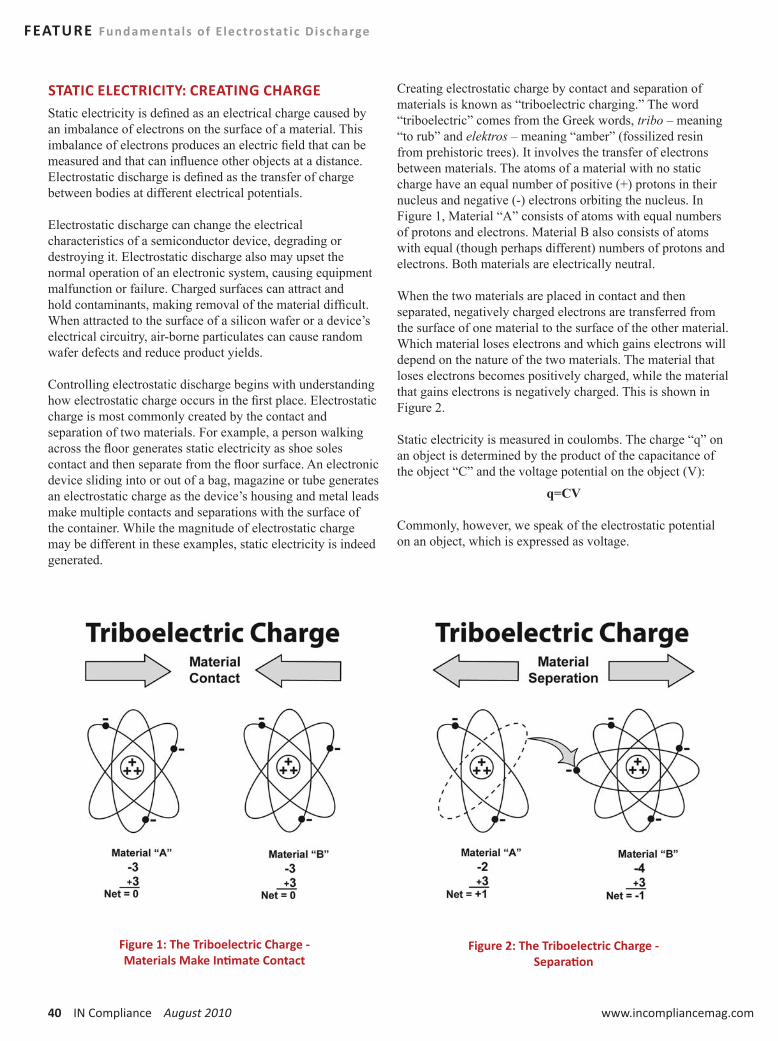
40 IN Compliance August 2010 www.incompliancemag.com
FEATURE Fundamentals of E lectrostat ic Discharge
STATIC ELECTRICITY: CREATING CHARGEStatic electricity is defined as an electrical charge caused by an imbalance of electrons on the surface of a material. This imbalance of electrons produces an electric field that can be measured and that can influence other objects at a distance. Electrostatic discharge is defined as the transfer of charge between bodies at different electrical potentials.
Electrostatic discharge can change the electrical characteristics of a semiconductor device, degrading or destroying it. Electrostatic discharge also may upset the normal operation of an electronic system, causing equipment malfunction or failure. Charged surfaces can attract and hold contaminants, making removal of the material difficult. When attracted to the surface of a silicon wafer or a device’s electrical circuitry, air-borne particulates can cause random wafer defects and reduce product yields.
Controlling electrostatic discharge begins with understanding how electrostatic charge occurs in the first place. Electrostatic charge is most commonly created by the contact and separation of two materials. For example, a person walking across the floor generates static electricity as shoe soles contact and then separate from the floor surface. An electronic device sliding into or out of a bag, magazine or tube generates an electrostatic charge as the device’s housing and metal leads make multiple contacts and separations with the surface of the container. While the magnitude of electrostatic charge may be different in these examples, static electricity is indeed generated.
Creating electrostatic charge by contact and separation of materials is known as “triboelectric charging.” The word “triboelectric” comes from the Greek words, tribo – meaning “to rub” and elektros – meaning “amber” (fossilized resin from prehistoric trees). It involves the transfer of electrons between materials. The atoms of a material with no static charge have an equal number of positive (+) protons in their nucleus and negative (-) electrons orbiting the nucleus. In Figure 1, Material “A” consists of atoms with equal numbers of protons and electrons. Material B also consists of atoms with equal (though perhaps different) numbers of protons and electrons. Both materials are electrically neutral.
When the two materials are placed in contact and then separated, negatively charged electrons are transferred from the surface of one material to the surface of the other material. Which material loses electrons and which gains electrons will depend on the nature of the two materials. The material that loses electrons becomes positively charged, while the material that gains electrons is negatively charged. This is shown in Figure 2.
Static electricity is measured in coulombs. The charge “q” on an object is determined by the product of the capacitance of the object “C” and the voltage potential on the object (V):
q=CV
Commonly, however, we speak of the electrostatic potential on an object, which is expressed as voltage.
Figure 1: The Triboelectric Charge - Materials Make Intimate Contact
Figure 2: The Triboelectric Charge - Separation


42 IN Compliance August 2010 www.incompliancemag.com
FEATURE Fundamentals of E lectrostat ic Discharge
This process of material contact, electron transfer and separation is a much more complex mechanism than described here. The amount of charge created by triboelectric generation is affected by the area of contact, the speed of separation, relative humidity, and chemistry of the materials, surface work function and other factors. Once the charge is created on a material, it becomes an “electrostatic” charge (if it remains on the material). This charge may be transferred from the material, creating an electrostatic discharge, or ESD, event. Additional factors, such as the resistance of the actual
discharge circuit and the contact resistance at the interface between contacting surfaces also affect the actual charge that is released. Typical charge generation scenarios and the resulting voltage levels are shown in Table 1. In addition, the contribution of humidity to reducing charge accumulation is also shown. It should be noted however that static generation still occurs even at high relative humidity.
An electrostatic charge also may be created on a material in other ways such as by induction, ion bombardment, or contact with another charged object. However, triboelectric charging is the most common.
HOW MATERIAL CHARACTERISTICS AFFECT STATIC CHARGE
Triboelectric Series
When two materials contact and separate, the polarity and magnitude of the charge are indicated by the materials’ positions in a triboelectric series. The triboelectric series tables show how charges are generated on various materials. When two materials contact and separate, the one nearer the top of the series takes on a positive charge, the other a negative charge. Materials further apart on the table typically generate a higher charge than ones closer together. These tables, however, should only be used as a general guide because there are many variables involved that cannot be controlled well enough to ensure repeatability. A typical triboelectric series is shown in Table 2.
Virtually all materials, including water and dirt particles in the air, can be triboelectrically charged. How much charge is generated, where that charge goes, and how quickly, are functions of the materials’ physical, chemical and electrical characteristics.
Insulative Materials
A material that prevents or limits the flow of electrons across its surface or through its volume is called an insulator. Insulators have an extremely high electrical resistance, generally greater than 1 x 10¹¹ ohms (surface resistance) and 1 x 10¹¹ ohm-cm (volume resistivity). A considerable amount of charge can be generated on the surface of an insulator. Because an insulative material does not readily allow the flow of electrons, both positive and negative charges can reside on insulative surface at the same time, although at different locations. The excess electrons at the negatively charged spot might be sufficient to satisfy the absence of electrons at the positively charged spot. However, electrons cannot easily flow across the insulative material’s surface, and both charges may remain in place for a very long time.
Means of Generation 10-25% RH 65-90% RH
Walking across carpet 35,000V 1,500V
Walking across vinyl tile 12,000V 250V
Worker at bench 6,000V 100V
Poly bag picked up from bench 20,000V 1,200V
Chair with urethane foam 18,000V 1,500V
Table 1: Examples of Static GenerationTypical Voltage Levels
+
Positive
Negative
-
Rabbit fur
Glass
Mica
Human Hair
Nylon
Wool
Fur
Lead
Silk
Aluminum
Paper
COTTON
Steel
Wood
Amber
Sealing Wax
Nickel, copper Brass, silver
Gold, platinum
Sulfur
Acetate rayon
Polyester
Celluloid
Silicon
Teflon
Table 2: Typical Triboelectric Series

August 2010 IN Compliance 43
Fundamentals of E lectrostat ic Discharge FEATURE
Conductive Materials
A conductive material, because it has low electrical resistance, allows electrons to flow easily across its surface or through its volume. Conductive materials have low electrical resistance, less than 1 x 10⁴ ohms (surface resistance) and 1 x 10⁴ ohm (volume resistance) for electrostatic discussions. When a conductive material becomes charged, the charge (i.e., the deficiency or excess of electrons) will be uniformly distributed across the surface of the material. If the charged conductive material makes contact with another conductive material, the electrons will be shared between the materials quite easily. If the second conductor is attached to an earth grounding point, the electrons will flow to ground and the excess charge on the conductor will be “neutralized.”
Electrostatic charge can be created triboelectrically on conductors the same way it is created on insulators. As long as the conductor is isolated from other conductors or ground, the static charge will remain on the conductor. If the conductor is grounded, the charge will easily go to ground. Or, if the charged conductor contacts another conductor, the charge will flow between the two conductors.
Static Dissipative Materials
Static dissipative materials have an electrical resistance between insulative and conductive materials (1 x 10⁴ - 1 x 10¹¹ ohms surface or volume resistance). There can be electron flow across or through the dissipative material, but it is controlled by the surface resistance or volume resistance of the material.
As with the other two types of materials, charge can be generated triboelectrically on a static dissipative material. However, like the conductive material, the static dissipative material will allow the transfer of charge to ground or other conductive objects. The transfer of charge from a static dissipative material will generally take longer than from a conductive material of equivalent size. Charge transfers from static dissipative materials are significantly faster than from insulators, and slower than from conductors.
Electrostatic Fields
Charged materials also have an electrostatic field and lines of force associated with them. Conductive objects brought into the vicinity of this electric field will be polarized by a process known as induction. A negative electric field will repel electrons on the surface of the conducting item that is exposed to the field. A positive electric field will attract electrons to near the surface thus leaving other areas positively charged. No change in the actual charge on the item will occur in polarization. If, however, the item is conductive or dissipative and is touched to ground while polarized, charge will flow from or to ground to compensate for the charge imbalance. If the electrostatic field is removed and the ground contact
disconnected, the charge will be trapped on the item. If a nonconductive object is brought into the electric field, the electrical dipoles will tend to align with the field creating apparent surface charges. A nonconductor cannot be charged by induction.
ESD DAMAGE—HOW DEVICES FAILElectrostatic damage to electronic devices can occur at any point from manufacture to field service. Damage results from handling the devices in uncontrolled surroundings or when poor ESD control practices are used. Generally damage is classified as either a catastrophic failure or a latent defect.
Catastrophic Failure
When an electronic device is exposed to an ESD event, it may no longer function. The ESD event may have caused a metal melt, junction breakdown, or oxide failure. The device’s circuitry is permanently damaged causing the device to stop functioning. Such failures usually can be detected when the device is tested before shipment. If a damaging level ESD event occurs after test, the part may go into production and the damage will go undetected until the device fails in final test.
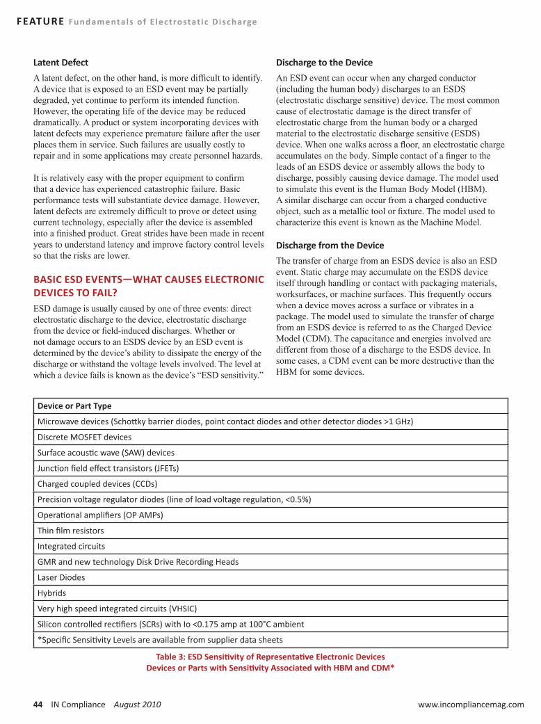
44 IN Compliance August 2010 www.incompliancemag.com
FEATURE Fundamentals of E lectrostat ic Discharge
Latent Defect
A latent defect, on the other hand, is more difficult to identify. A device that is exposed to an ESD event may be partially degraded, yet continue to perform its intended function. However, the operating life of the device may be reduced dramatically. A product or system incorporating devices with latent defects may experience premature failure after the user places them in service. Such failures are usually costly to repair and in some applications may create personnel hazards.
It is relatively easy with the proper equipment to confirm that a device has experienced catastrophic failure. Basic performance tests will substantiate device damage. However, latent defects are extremely difficult to prove or detect using current technology, especially after the device is assembled into a finished product. Great strides have been made in recent years to understand latency and improve factory control levels so that the risks are lower.
BASIC ESD EVENTS—WHAT CAUSES ELECTRONIC DEVICES TO FAIL?ESD damage is usually caused by one of three events: direct electrostatic discharge to the device, electrostatic discharge from the device or field-induced discharges. Whether or not damage occurs to an ESDS device by an ESD event is determined by the device’s ability to dissipate the energy of the discharge or withstand the voltage levels involved. The level at which a device fails is known as the device’s “ESD sensitivity.”
Discharge to the Device
An ESD event can occur when any charged conductor (including the human body) discharges to an ESDS (electrostatic discharge sensitive) device. The most common cause of electrostatic damage is the direct transfer of electrostatic charge from the human body or a charged material to the electrostatic discharge sensitive (ESDS) device. When one walks across a floor, an electrostatic charge accumulates on the body. Simple contact of a finger to the leads of an ESDS device or assembly allows the body to discharge, possibly causing device damage. The model used to simulate this event is the Human Body Model (HBM). A similar discharge can occur from a charged conductive object, such as a metallic tool or fixture. The model used to characterize this event is known as the Machine Model.
Discharge from the Device
The transfer of charge from an ESDS device is also an ESD event. Static charge may accumulate on the ESDS device itself through handling or contact with packaging materials, worksurfaces, or machine surfaces. This frequently occurs when a device moves across a surface or vibrates in a package. The model used to simulate the transfer of charge from an ESDS device is referred to as the Charged Device Model (CDM). The capacitance and energies involved are different from those of a discharge to the ESDS device. In some cases, a CDM event can be more destructive than the HBM for some devices.
Device or Part Type
Microwave devices (Schottky barrier diodes, point contact diodes and other detector diodes >1 GHz)
Discrete MOSFET devices
Surface acoustic wave (SAW) devices
Junction field effect transistors (JFETs)
Charged coupled devices (CCDs)
Precision voltage regulator diodes (line of load voltage regulation, <0.5%)
Operational amplifiers (OP AMPs)
Thin film resistors
Integrated circuits
GMR and new technology Disk Drive Recording Heads
Laser Diodes
Hybrids
Very high speed integrated circuits (VHSIC)
Silicon controlled rectifiers (SCRs) with Io <0.175 amp at 100°C ambient
*Specific Sensitivity Levels are available from supplier data sheets
Table 3: ESD Sensitivity of Representative Electronic DevicesDevices or Parts with Sensitivity Associated with HBM and CDM*
August 2010 IN Compliance 45
Fundamentals of E lectrostat ic Discharge FEATURE
The trend towards automated assembly would seem to solve the problems of HBM ESD events. However, it has been shown that components may be more sensitive to damage when assembled by automated equipment. A device may become charged, for example, from sliding down the feeder. If it then contacts the insertion head or another conductive surface, a rapid discharge occurs from the device to the metal object.
Field Induced Discharges
Another electrostatic charging process that can directly or indirectly damage devices is termed Field Induction. As noted earlier, whenever any object becomes electrostatically charged, there is an electrostatic field associated with that charge. If an ESDS device is placed in that electrostatic field, a charge may be induced on the device. If the device is then momentarily grounded while within the electrostatic field, a transfer of charge from the device occurs as a CDM event. If the device is removed from the region of the electrostatic field and grounded again, a second CDM event will occur as charge (of opposite polarity from the first event) is transferred from the device.
HOW MUCH STATIC PROTECTION IS NEEDED?Damage to an ESDS device by the ESD event is determined by the device’s ability to dissipate the energy of the discharge or withstand the voltage levels involved—as explained previously these factors determine the parts ESD sensitivity. Defining the ESD sensitivity of electronic components is the first step in determining the degree of ESD protection required. Test procedures based on the models of ESD events help define the sensitivity of components to ESD. These procedures and more are covered in Part 5 of this series.Many electronic components are susceptible to ESD damage at relatively low voltage levels. Many are susceptible at less than 100 volts, and many disk drive components have sensitivities below 10 volts. Current trends in product design and development pack more circuitry onto these miniature devices, further increasing their sensitivity to ESD and making the potential problem even more acute. Table 3 indicates the ESD sensitivity of various types of components.
SUMMARYIn this introductory article on electrostatic discharge, we have discussed the basics of electrostatic charge and discharge, types of failures, ESD events, and device sensitivity. We can summarize this discussion as follows:
1. Virtually all materials, even conductors, can be triboelectrically charged.
2. The level of charge is affected by material type, speed of contact and separation, humidity, and several other factors.
3. Electrostatic fields are associated with charged objects.
4. Electrostatic discharge can damage devices so they fail immediately, or ESD may result in latent damage that may escape immediate detection, but cause the device to fail prematurely once in service.
5. Electrostatic discharge can occur throughout the manufacturing, test, shipping, handling, or operational processes.
6. Component damage can occur as the result of a discharge to the device, from the device, or from charge transfers resulting from electrostatic fields. Devices vary significantly in their sensitivity to ESD.
Protecting your products from the effects of static damage begins by understanding these key concepts of ESD. Armed with this information, you can then begin to develop an effective ESD control program. In Part 2 we will focus on some basic concepts of ESD control. n REFERENCES1. ESD-ADV 1.0, Glossary, ESD Association, Rome NY.
2. ESD TR20.20, Handbook, ESD Association, Rome, NY.
3. ESD ADV 11.2, Triboelectric Charge Accumulation Testing, ESD Association, Rome, NY.
4. ANSI/ESD S20.20—Standard for the Development of Electrostatic Discharge Control Program, ESD Association, Rome, NY.
© 2010, ESD Association, Rome, NY

46 IN Compliance August 2010 www.incompliancemag.com
Components Directory
ABSORBERS SHIELDED COATINGS
BOARD LEVEL SHIELDING
CONDUCTIVE MATERIALS
LEADER TECH INC. . . . . . . . . . . . . . . . . . . . . . . .866-TECH-EMI
FERRITE BEADS, RODS & FORMS
LEADER TECH INC. . . . . . . . . . . . . . . . . . . . . . . .866-TECH-EMI
FILTERS
SHIELDED ENCLOSURES
SHIELDED WIRE AND CABLE
SHIELDING MATERIAL

August 2010 IN Compliance 47
Outstanding Service Recognition Program Announced
ANSI Accredited Standards Committee on Electromagnetic Compatibility, C63®, has initiated a program to recognize individuals who have given outstanding service to the C63® committee over an extended period of time.
Nominees for the C63® Outstanding Contribution Award shall be past or current members of C63® and/or its subcommittees and/or working groups, and shall have demonstrated a significant contribution to the activities of C63® over a period of at least 5 years.
The Awards Committee is soliciting the names of prospective awardees by means of announcements at C63® meetings and in the C63 ® Newsletter, and by e-mail notices to all C63® participants. Nominations should be sent to the chairman of the Awards Committee, [email protected], and should include a short description of why the person is being nominated. The deadline for receiving nominations that will be considered for the Thursday, October 28, 2010, C63® general meeting is Monday, August 16, 2010.The Awards Committee will review all nominations and make their recommendations to the C63® Steering Committee approximately 6 weeks prior to the Thursday, October 28, 2010 C63® general meeting. A maximum of two persons will be recommended to the Steering Committee by the Awards Committee each calendar year.
The Steering Committee may choose to approve none, one, or both of the Awards Committee nominees. The individuals receiving recognition will receive a Certificate of Appreciation signed by the Chairman of C63® and a monetary award valued at approximately $50.00 USD or a dinner for two. The Certificate will be presented by the chairman of C63® at the C63® general meeting on October 28 and an announcement will be made in the C63® newsletter. If requested by the awardee, a letter of appreciation may also be sent to their employer, signed by the chairman of C63®.
New Extended Temperature COTS for Rugged, Continuous Operation Applications
LCR Electronics, has introduced a line of single phase COTS (commercial-off-the-shelf) filters that operates over an extended temperature range of -40°C to +85°C (-40°F to +185°F).
The new RoHS-compliant Single Stage F9100 Filters and Double Stage F9200 Filters are ideal for high ambient environments or in applications with limited temperature rise requirements as found in the military, industrial and medical industries.
The new 115/250 VAC 50/60 Hz filters are available with rated current from 5 A to 35 A, in both general purpose and low leakage current versions. High potential voltage for both series is 1,450 VDC line-to-line and 2,250 VDC line-to-ground. Depending on the filter current rating,
insertion loss for the F9100 measured in a 50 ohm system for frequencies starting at 50 kHz up to 30 MHz ranges from 5 dB to 45 dB in common mode and 5 dB to 35 dB in differential mode. Insertion loss for the F9200 ranges from 5 dB to 80 dB in common mode and 10 dB to 75 dB in differential mode, under the same conditions. For more information, visit www.lcr-inc.com/military-filters.html.
West Coast Operations Expansion
Leader Tech announces the expansion of its West Coast operations. Alex Cox, the Company’s newest Regional Sales Engineer, will lead this effort from his San Francisco Bay Area office.
“The addition of Alex to our team will allow Leader Tech to strengthen existing client relationships and dramatically improve one-on-one engineering support for customers in the Western United States,” says Tim Black, Director of Business Development.
Alex brings 15 years of technical sales experience in the electronics industry and has extensive working knowledge of Defense Aerospace, Wireless, RF Microwave, Telecommunication, and Semiconductor applications. Immediately prior to joining Leader Tech, Alex amassed a decade of hands-on experience with a major electronic equipment company. During that tenure, he provided R&D, Electrical, and Design Engineering teams with highly-responsive engineering and customer service support.
BUSINESS NEWS
Bob Hofmann, Chairman of the ASC-C63® Awards Committee (left) is shown receiving his Membership
Certificate from the Chairman of ASC-C63®, Don Heirman, during the April, 2010 meeting in Piscataway, NJ.
48 IN Compliance August 2010 www.incompliancemag.com
BUSINESS NEWS
Low Frequency Magnetic Shielding Coating
Integran Technologies Inc. has entered into an exclusive, Worldwide, Market Development Agreement (MDA) with Magnetic Shield Corporation to provide Nanovate™ EM coating for low frequency magnetic shielding.
Nanovate™ EM coating technology achieves similar performance to specialty discrete magnetic shielding foils currently offered by Magnetic Shield Corporation, but uses a process that allows a nanocrystalline metal to be applied directly to metal, polymer and composite substrates. The process flexibility enables appli-cations where part size, and/or complexity makes the use of formed foils impractical. In addition, the Nanovate™ EM coating also eliminates additional processes such as forming, annealing and assembly. “We see tremendous promise in the Nanovate EM coating when considering the decreasing size and increasing complexity of certain part applications.”, says Mark Wickler, COO of Magnetic Shield Corporation.
Magnetic Shield Corporation reports that companies working with sensors, transducers, and other electronic devices sensitive to low frequency magnetic interference will be particularly interested in this novel approach. To learn more about Nanovate™ EM, visit www.magnetic-shield.com/nano.html.
Advanced Compliance Solutions Inc. Completes Audit to Become CBTL
Advanced Compliance Solutions (ACS) has partnered with Nemko USA for assistance and sponsorship of their CB Testing Laboratory (CBTL) program. After a successful audit by three international members of the CB Scheme, ACS is now capable of testing and generating a CB report which is provided to NCB Nemko for issuance of the internationally recognized CB Certificate. The CB Report is then used by the manufacturer to gain national certification in over 50 countries without the need for in-country re-testing.
Nemko works with ACS as a partner lab, a non-exclusive relationship whereby both organizations benefit from cooperative business activity. The Nemko Direct Market Access program ACS uses frequently is a valued service for global approvals that perfectly complimented ACS’s entry into the CB Scheme.
“ACS now offers a complete test and approval process for customers with global aspirations” explains Doug Massey, Director of Safety at ACS. “ACS can depend on Nemko’s involvement and guidance from the test plan phase through the issuance of the CB Certificate and leverage of that report for other mandatory national certifications.”
Flexible 3 GHz EMI Digital Receiver
Teseq Inc. has introduced a cost-effective, high-performance digital EMI receiver/analyzer with optimum measurement parameters for those EMC labs that do not require full CISPR compliance for radiated emissions measurements. The new PMM 9010/30P features a frequency measurement range of 10 Hz up to 3 GHz for labs with smaller test chambers, GTEM (gigahertz transverse electromagnetic) cells or doing on-site work, and is fully compliant to CISPR 16-1-1 in the 9 kHz to 30 MHz measurement range. When paired with a PMM extension receiver module, the PMM 9010/30P becomes fully
CISPR-compliant measuring up to 6 GHz. Teseq is the exclusive North American distributor for PMM, a brand of Narda Safety Test Solutions srl, which manufactures the compact modular PMM 9010/30P receiver.
The flexible PMM 9010/30P provides more stable performance than analog receivers. It uses powerful digital signal processing to eliminate aging of critical parts that could degrade measurement accuracy. The CISPR detectors as well as the IF and RBW filters are completely stable and feature lifetime, calibration-free operation. The PMM 9010 series receivers include the latest CISPR 16 detectors, including RMS-AVG, C-AVG and APD, as well as the traditional Peak, Quasi-Peak and AVG detectors. Internal preamplifier, peak limiter and attenuator systems are also included. For the CISPR 16 compliant ranges, an integrated tracking pre-selector is included.
The new receiver is ideal for use in small labs and commercial test labs that have limited budgets, but need to perform fast, reliable, compliant measurements. Using the CLICK option, non-continuous operating household appliances such as mixers and hair dryers can be rapidly pre-tested for compliance to CISPR 14. For more information, visit www.teseq.com.
Solar Panel Modules Donated for SolarAid Mission
More than 150,000 people now have access to clean and safe renewable energy amid the rural landscape of Tanzania, Africa, thanks to a generous donation of 200 solar panels by TÜV Rheinland PTL, LLC, part of the world’s
August 2010 IN Compliance 49
largest solar and photovoltaic testing network. The recycled modules are being installed by SolarAid, a British charity determined to reduce global poverty and climate change through solar energy.
To date, SolarAid has installed 70 of the donated solar modules onto the roofs of 14 health facilities in the Iringa region of central Tanzania. According to SolarAid (www.solar-aid.org), the modules produce 12.6 KW of power for the structures, which serve an estimated 154,586 people. SolarAid plans to set up the remaining 130 modules onto 22 – 27 health facilities and clinics in Iringa, Ludewa, Makete, and Kiwango over the next year.
TÜV Rheinland PTL has been donating modules to individuals and organizations for 12 years. These modules no longer have commercial value after completing a cycle of qualification and engineering testing at TÜV Rheinland PTL’s photovoltaic testing laboratory in Tempe, Arizona. Per an agreement with the manufacturers, TÜV Rheinland PTL recycles the tested panels for educational or nonprofit purposes, primarily to expand awareness and share the benefits of renewable energy.
Over 85 percent of Tanzanians have no access to electricity, primarily relying on wood and charcoal for cooking, kerosene and candles for lighting, and disposable batteries for radios and other handheld electrical devices. More than one-third of the population lives below the national poverty line, further limiting their ability to attain clean, safe and reliable forms of energy.
According to SolarAid, many of the health facilities have been using battery-powered torches as examination lights and illuminating rooms with dimly lit kerosene-filled tins. With solar energy, the clinics have expanded to a 24-hour operation and increased their ability to save lives and reduce illness.
The donated modules were made by a variety of manufacturers including Soluxia; Canadian Solar Inc; Mitsubishi; Boading Tainwei; MSK; Suntech; Brightwatts; Schott; Shell; BP Solar; Evergreen; Solarfun; Sunpower; and Solar World. For more information, visit www.tuvptl.com.
TÜV SÜD Appoints Business Development Director
TÜV SÜD is pleased to announce that Mr. Leeton H. Lee has joined the company’s Consumer Goods and Retail Services group in the role of Business Development Director. Mr. Lee’s appointment helps further strengthen TÜV SÜD’s testing, inspection, and certification program for toys, children’s products, apparel, and footwear in the America’s region.
Mr. Lee joins TÜV SÜD America with over 15 years of experience in product safety compliance, quality assurance, risk management and safety recalls in the key areas of toys, children’s products, premiums, promotional products, apparel, and other consumer products. He has many years of experience as an in-house legal counsel for well-known toy and consumer products companies, along with having established and supervised the companies’ in-house product compliance, safety, and quality assurance departments.
Test Center Awarded ISO/IEC 17025 Accreditation from A2LA
Renewable Energy Test Center, TÜV SÜD America’s partner for Photovoltaics Testing, has announced that it has been awarded ISO/IEC 17025 accreditation from The American Association for Laboratory Accreditation (A2LA). The scope of the ISO/IEC 17025 accreditation applies to all IEC and UL Test Standards required for PV certification, and includes:
y IEC 61215 for c-Si Flat-Plate Panels
y IEC 61646 for Thin Film Flat-Plate Panels
y IEC 62108 for Concentrator PV
y IEC 61730 Standard for Safety for Flat-Plate Panels (Europe)
y IEC 60904 Standard for Cell Testing and Characterization
y UL 1703 Standard for Safety for Flat-Plate Panels (USA)
y ULC/ORD C-1703 Standard for Safety for Flat-Plate Panels (Canada)
“Leveraging on RETC’s vast experience in equipment design and fabrication, process development, PV Testing, and Quality Standards, RETC was able to successfully achieve its ISO/IEC 17025 accreditation in a brief three-month period, soon after the official move into our 26,000-square-foot, state-of-the-art PV Testing Laboratory in the heart of the Silicon Valley,” states Ms. Alelie Funcell, President and CEO, RETC, LLC. “Our broad range of PV Testing Services, which includes listing to UL 1703 by a NRTL, and ISO/IEC 17025 A2LA accreditation, qualifies us to become an ILAC-Affiliated Laboratory. RETC is now listed by The California Energy Commission (CEC) as one of the ILAC-Affiliated Laboratories for PV.”
“TÜV SÜD America is also in the process of obtaining ULC/ORD C-1703 Accreditation from Standards Council of Canada (SCC) through its partnership with RETC. With the lengthy turn-around times of PV testing and certification both in the U.S. and globally, this additional milestone demonstrates the two organizations’ drive to further the advancements of solar energy technologies,” added Mr. Karsten Xander, President and CEO, TÜV SÜD America. For more information, visit www.tuvamerica.com/services/photovoltaics.cfm.
BUSINESS NEWS

50 IN Compliance August 2010 www.incompliancemag.com
2010 Minnesota EMC Event. . . . . . . . . . . . .45
AMTA 2010 Regional Event . . . . . . . . . . . . .43
AR. . . . . . . . . . . . . . . . . . . . . . . . . . . . . . . . . .11
Braden Shielding Systems . . . . . . . . . . . . . .C4
Captor Corporation. . . . . . . . . . . . . . . . . . . .35
Com-Power Corporation . . . . . . . . . . . . . . .C2
Curtis Industries/Filter Networks . . . . . . . .13
E. D. & D., Inc. . . . . . . . . . . . . . . . . . . . . . . . .21
ESD Association. . . . . . . . . . . . . . . . . . . . . . .41
ETS-Lindgren . . . . . . . . . . . . . . . . . . . . . . . . .C3
Nemko Canada . . . . . . . . . . . . . . . . . . . . . . .27
Panashield, Inc. . . . . . . . . . . . . . . . . . . . . . . .29
Schurter Elecronic Components . . . . . . . . .19
Spira Manufacturing Corporation . . . . . . . .33
EVENTS
August 4Test Area and Personnel/Common Electrical Product Safety Tests SeminarAssociated Research, Inc. Lake Forest, ILwww.incompliancemag.com/events/100804
August 11Operator Safety in Electrical Safety TestingAssociated Research, Inc. Webinarwww.incompliancemag.com/events/100811
August 12Data Acceptance Program and ISO/IEC 17025 Requirements and ImplementationUL UniversityResearch Triangle Park, NCwww.incompliancemag.com/events/100812
August 16 – August 17Critical EMC Concepts for Meeting Radiated Immunity RequirementsNational Technical Systems, Inc.Plano, TXwww.incompliancemag.com/events/100816_1
August 16 – August 19MIL-STD-461F: Methods and ProceduresWL Academy Gaithersburg, MDwww.incompliancemag.com/events/100816_2
August 17 – August 18 Lightning Protection Installation Standard ReviewUL UniversityResearch Triangle Park, NCwww.incompliancemag.com/events/100817
August 24Advances in Antenna Test and Measurement: A Colloquium and ExhibitionAMTA/IEEE SE Michigan and Dayton SectionsDayton, OHwww.incompliancemag.com/events/100824_1
August 24 – August 25Globalability: The Key to International ComplianceUL UniversityNorthbrook, ILwww.incompliancemag.com/events/100824_2
August 25Medical Device Testing Associated Research, Inc. Webinarwww.incompliancemag.com/events/100825
ADVERTISERS
Advertiser Page Advertiser Page
Seminars, Training &
Symposiums