tgf2929-hm datasheet
TRANSCRIPT

TGF2929-HM 100W, 28V, DC – 3.5 GHz, GaN RF Power Transistor
Data Sheet Rev. C, February 2020 | Subject to change without notice
1 of 19 www.qorvo.com
Product Features • Frequency: DC to 3.5 GHz
• Output Power (P3dB)1: 132 W
• Linear Gain1: 17.4 dB
• Typical DEFF (P3dB)1: 74.9%
• Operating Voltage: 28 V
• Low thermal resistance package
• CW and Pulse capable
Note 1: @ 2 GHz
General Description The Qorvo TGF2929-HM is a 100 W (P3dB) discrete GaN on
SiC HEMT which operates from DC to 3.5 GHz. The
device is constructed with Qorvo’s proven QGaN25HV
process, which features advanced field plate techniques to
optimize power and efficiency at high drain bias operating
conditions. This optimization can potentially lower system
costs in terms of fewer amplifier line-ups and lower thermal
management costs.
Hermetic package
Lead-free and ROHS compliant
Evaluation boards are available upon request.
Functional Block Diagram
Applications • Space radar
• Satcomm
• Military radar
• Civilian radar
• Land mobile and military radio communications
• Test instrumenation
• Wideband or narrowband amplifiers
• Jammers
Ordering info Part No. Description TGF2929-HM DC – 3.5 GHz packaged part
TGF2929-HM EVB01 3.1 – 3.5 GHz EVB

TGF2929-HM 100W, 28V, DC – 3.5 GHz, GaN RF Power Transistor
Data Sheet Rev. C, February 2020 | Subject to change without notice
2 of 19 www.qorvo.com
Absolute Maximum Ratings Parameter Rating Units
Breakdown Voltage,BVDG +145 V
Gate Voltage Range, VG −7 to +2 V
Drain Current 12 A
Power Dissipation, CW (PDISS) See page 4. W
RF Input Power, CW, T=25 °C +42 dBm
Storage Temperature −65 to +150 °C
Exceeding any one or a combination of the Absolute Maximum Rating conditions may cause permanent damage to the device. Extended application of Absolute Maximum Rating conditions to the device may reduce device reliability.
Recommended Operating Conditions Parameter Min Typ Max Units
Drain Voltage Range, VD +12 +28 +50 V
Drain Bias Current, IDQ – 260 – mA
Gate Voltage, VG1 – −2.7 – V
Electrical specifications are measured at specified test conditions. Specifications are not guaranteed over all recommended operating conditions. Notes:
1. To be adjusted to desired IDQ
Electrical Specifications Parameter Conditions Min Typ Max Units
Gate Leakage VD = +10, VG = −3.8 −31.7 mA

TGF2929-HM 100W, 28V, DC – 3.5 GHz, GaN RF Power Transistor
Data Sheet Rev. C, February 2020 | Subject to change without notice
3 of 19 www.qorvo.com
Pulsed Characterization – Load Pull Performance – Efficiency Tuned1 Parameters Typical Values Unit
Frequency 1 2 3 3.5 GHz
Linear Gain, GLIN 23.3 18.6 16.0 17 dB
Output Power at 3dB compression point, P3dB
50.1 49.5 49.9 49.1 dBm
Drain Efficiency at 3dB compression point, DEFF3dB
79.2 74.9 67.4 63.1 %
Gain at 3dB compression point, G3dB
20.3 15.6 13.0 14 dB
Notes: 1. VD = +28 V, ID = 260 mA, Temp = +25 °C, Pulse Width = 100 uS, Duty Cycle = 20%
Pulsed Characterization – Load Pull Performance – Power Tuned1 Parameters Typical Values Unit
Frequency, F 1 2 3 3.5 GHz
Linear Gain, GLIN 21.7 17.4 14.7 15.6 dB
Output Power at 3dB compression point, P3dB
50.9 51.2 50.9 50.8 dBm
Drain Efficiency at 3dB compression point, DEFF3dB
69.4 68.1 59.7 58.5 %
Gain at 3dB compression point 18.7 14.4 11.7 12.6 dB
Notes: 1. VD = +28 V, ID = 260 mA, Temp = +25 °C, Pulse Width = 100 uS, Duty Cycle = 20%
RF Characterization – 3.1 – 3.5 GHz EVB Performance At 3.3 GHz1 Parameter Min Typ Max Units
Linear Gain, GLIN – 13.9 – dB
Output Power at 3dB compression point, P3dB – 50.5 – dBm
Power-Added-Efficiency at 3dB compression point, PAE3dB
– 54 – %
Gain at 3dB compression point, G3dB – 10.9 – dB
Notes: 1. VD = +28 V, ID = 260 mA, Temp = +25 °C, Pulse Width = 100 uS, Duty Cycle = 20%
RF Characterization – Mismatch Ruggedness at 3.3 GHz Symbol Parameter dB Compression Typical
VSWR Impedance Mismatch Ruggedness 3 10:1
Test conditions unless otherwise noted: TA = 25 °C, VD = 28 V, IDQ = 260 mA, Pulse Width = 100 uS, Duty Cycle = 20%, Driving input power is determined at pulsed compression under matched condition at EVB output connector.

TGF2929-HM 100W, 28V, DC – 3.5 GHz, GaN RF Power Transistor
Data Sheet Rev. C, February 2020 | Subject to change without notice
4 of 19 www.qorvo.com
Thermal and Reliability Information – Pulsed
Thermal and Reliability Information – CW
100.0
110.0
120.0
130.0
140.0
150.0
160.0
170.0
180.0
190.0
200.0
1.00E-06 1.00E-05 1.00E-04 1.00E-03 1.00E-02 1.00E-01 1.00E+00
Pe
ak IR
Su
rfac
e T
em
pe
ratu
re (°
C)
Pulse Width (sec)
Peak IR Surface TemperaturePackage base fixed at 85°C, Pdiss = 100 W
5% Duty Cycle 10% Duty Cycle 20% Duty Cycle 50% Duty Cycle
80
100
120
140
160
180
200
220
240
0 10 20 30 40 50 60 70 80 90 100 110 120
Pe
ak I
R S
urf
ace
Te
mp
era
ture
, °C
CW Power Dissipation, W
Peak IR SurfaceTemperature vs. CW PowerPackage base fixed at 85°C

TGF2929-HM 100W, 28V, DC – 3.5 GHz, GaN RF Power Transistor
Data Sheet Rev. C, February 2020 | Subject to change without notice
5 of 19 www.qorvo.com
Thermal and Reliability Information – CW
Parameter Simulation Conditions Value Units
Thermal Resistance, Peak IR Surface Temperature at Average Power (θJC) PDISS = 28.8 W, Tbaseplate = 85 °C
1.08 °C/W
Channel Temperature (TCH) 116 °C
Thermal Resistance, Peak IR Surface Temperature at Average Power (θJC) PDISS = 57.6 W, Tbaseplate = 85 °C
1.15 °C/W
Channel Temperature (TCH) 151 °C
Thermal Resistance, Peak IR Surface Temperature at Average Power (θJC) PDISS = 86.4 W, Tbaseplate = 85 °C
1.20 °C/W
Channel Temperature (TCH) 189 °C
Thermal Resistance, Peak IR Surface Temperature at Average Power (θJC) PDISS = 115.2 W, Tbaseplate = 85 °C
1.28 °C/W
Channel Temperature (TCH) 232 °C
Note: 1. Thermal resistance measured to bottom of package. 2. Refer to the following document: GaN Device Channel Temperature. Thermal Resistance, and Reliability Estimates
Thermal and Reliability Information – Pulsed
Parameter Simulation Conditions Value Units
Thermal Resistance, Peak IR Surface Temperature at Average Power (θJC)
PDISS = 100 W, Tbaseplate = 85 °C
Pulse Width = 1 mS
Duty Cycle = 5%
0.73 °C/W
Channel Temperature (TCH) 158 °C
Thermal Resistance, Peak IR Surface Temperature at Average Power (θJC)
PDISS = 100 W, Tbaseplate = 85 °C
Pulse Width = 1 mS
Duty Cycle = 10%
0.75 °C/W
Channel Temperature (TCH) 160 °C
Thermal Resistance, Peak IR Surface Temperature at Average Power (θJC)
PDISS = 100 W, Tbaseplate = 85 °C
Pulse Width = 1 mS
Duty Cycle = 20%
0.78 °C/W
Channel Temperature (TCH) 163 °C
Thermal Resistance, Peak IR Surface Temperature at Average Power (θJC)
PDISS = 100 W, Tbaseplate = 85 °C
Pulse Width = 1 mS
Duty Cycle = 50%
0.88 °C/W
Channel Temperature (TCH) 173 °C
Note: 1. Thermal resistance measured to bottom of package. 2. Refer to the following document: GaN Device Channel Temperature. Thermal Resistance, and Reliability Estimates

TGF2929-HM 100W, 28V, DC – 3.5 GHz, GaN RF Power Transistor
Data Sheet Rev. C, February 2020 | Subject to change without notice
6 of 19 www.qorvo.com
Load Pull Smith Charts1, 2, 3 Notes: 1. 28 V, 260 mA, Pulsed signal with 100 uS pulse width and 20 % duty cycle. Performance is at indicated input power.
2. See page 15 for load pull and source pull reference planes. 6-Ω load pull TRL fixtures are built with 20-mil RO4350B material. 3. NaN means the impedances are either undefined or varying in load-pull system.
0.4
0.5
0.6
0.7
0.8
0.9
1 1.2
1GHz, Load-pull
50.950.4
49.9
21.2
20.7
20.2
19.2
18.777.2
75.2
73.2
69.2
• Max Power is 50.9dBm
at Z = 2.74+0.08i
= -0.3729+0.0126i
• Max Gain is 21.3dB
at Z = 3.34+2.77i
= -0.1809+0.3502i
• Max DEff is 79.2%
at Z = 3.44+1.37i
= -0.245+0.1807i
Zo = 6
3dB Compression Referenced to Peak Gain
Zs(1fo) = 0.55-0.79i
Zs(2fo) = 0.45+0.23i
Zs(3fo) = 0.63+2.62i
Power
Gain
DEFF

TGF2929-HM 100W, 28V, DC – 3.5 GHz, GaN RF Power Transistor
Data Sheet Rev. C, February 2020 | Subject to change without notice
7 of 19 www.qorvo.com
Load Pull Smith Charts1, 2, 3 Notes: 1. 28 V, 260 mA, Pulsed signal with 100 uS pulse width and 20 % duty cycle. Performance is at indicated input power.
2. See page 15 for load pull and source pull reference planes. 6-Ω load pull TRL fixtures are built with 20-mil RO4350B material. 3. NaN means the impedances are either undefined or varying in load-pull system.
0.2
0.3
0.4
0.5
0.6
0.7
0.8
0.9
1 1.2
2GHz, Load-pull
50.8
50.3
49.8
16.2
15.7
15.2
14.2
74.3
72.3
70.368.3
• Max Power is 51.2dBm
at Z = 2.08-2.52i
= -0.3535-0.4221i
• Max Gain is 16.6dB
at Z = 1.75+0.48i
= -0.5425+0.0955i
• Max DEff is 74.9%
at Z = 1.81-1.13i
= -0.505-0.2178i
Zo = 6
3dB Compression Referenced to Peak Gain
Zs(1fo) = 1.01-5.12i
Zs(2fo) = 1.17-5.31i
Zs(3fo) = 1.77-6.3i
Power
Gain
DEFF

TGF2929-HM 100W, 28V, DC – 3.5 GHz, GaN RF Power Transistor
Data Sheet Rev. C, February 2020 | Subject to change without notice
8 of 19 www.qorvo.com
Load Pull Smith Charts1, 2, 3 Notes: 1. 28 V, 260 mA, Pulsed signal with 100 uS pulse width and 20 % duty cycle. Performance is at indicated input power.
2. See page 15 for load pull and source pull reference planes. 6-Ω load pull TRL fixtures are built with 20-mil RO4350B material. 3. NaN means the impedances are either undefined or varying in load-pull system.
-0.4
3GHz, Load-pull
50.550
49.5
48.5
14.2
13.7
13.2
11.7
66.6 64.6 62.6
58.6
• Max Power is 50.9dBm
at Z = 1.84-4.1i
= -0.2019-0.6285i
• Max Gain is 14.4dB
at Z = 0.98-1.29i
= -0.6624-0.3072i
• Max DEff is 67.4%
at Z = 1.56-3.05i
= -0.3651-0.5507i
Zo = 6
3dB Compression Referenced to Peak Gain
Zs(1fo) = 13.54-5.28i
Zs(2fo) = 12.79+6.84i
Zs(3fo) = 6.7+0.08i
Power
Gain
DEFF

TGF2929-HM 100W, 28V, DC – 3.5 GHz, GaN RF Power Transistor
Data Sheet Rev. C, February 2020 | Subject to change without notice
9 of 19 www.qorvo.com
Load Pull Smith Charts1, 2, 3 Notes: 1. 28 V, 260 mA, Pulsed signal with 100 uS pulse width and 20 % duty cycle. Performance is at indicated input power.
2. See page 15 for load pull and source pull reference planes. 6-Ω load pull TRL fixtures are built with 20-mil RO4350B material. 3. NaN means the impedances are either undefined or varying in load-pull system.
-0.5
3.5GHz, Load-pull
50.5
50
49.5
14.1
13.6
13.1
12.6
61.2
59.2
57.2
• Max Power is 50.8dBm
at Z = 1.49-4.74i
= -0.144-0.724i
• Max Gain is 14.5dB
at Z = 0.81-3.23i
= -0.4385-0.6823i
• Max DEff is 63.1%
at Z = 1.28-3.79i
= -0.2969-0.6752i
Zo = 6
3dB Compression Referenced to Peak Gain
Zs(1fo) = 2.55+1.69i
Zs(2fo) = 9.73+2.34i
Zs(3fo) = 10.83-9.97i
Power
Gain
DEFF
TGF2929-HM 100W, 28V, DC – 3.5 GHz, GaN RF Power Transistor
Data Sheet Rev. C, February 2020 | Subject to change without notice
10 of 19 www.qorvo.com
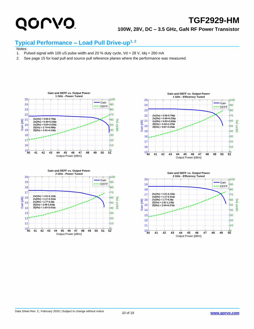
Typical Performance – Load Pull Drive-up1, 2 Notes: 1. Pulsed signal with 100 uS pulse width and 20 % duty cycle, Vd = 28 V, Idq = 260 mA
2. See page 15 for load pull and source pull reference planes where the performance was measured.
40 41 42 43 44 45 46 47 48 49 50 5115
16
17
18
19
20
21
22
23
24
25
Output Power [dBm]
Ga
in [d
B]
Gain and DEFF vs. Output Power1 GHz - Power Tuned
Zs(1fo) = 0.55-0.79i
Zs(2fo) = 0.45+0.23i
Zs(3fo) = 0.63+2.62i
Zl(1fo) = 2.74+0.08i
Zl(2fo) = 3.41+4.14i
40 41 42 43 44 45 46 47 48 49 50 510
10
20
30
40
50
60
70
80
90
100
DE
FF
[%
]
Gain
DEFF
40 41 42 43 44 45 46 47 48 49 50 5115
16
17
18
19
20
21
22
23
24
25
Output Power [dBm]
Ga
in [d
B]
Gain and DEFF vs. Output Power1 GHz - Efficiency Tuned
Zs(1fo) = 0.55-0.79i
Zs(2fo) = 0.45+0.23i
Zs(3fo) = 0.63+2.62i
Zl(1fo) = 3.44+1.37i
Zl(2fo) = 9.87+3.25i
40 41 42 43 44 45 46 47 48 49 50 510
10
20
30
40
50
60
70
80
90
100
DE
FF
[%
]
Gain
DEFF
40 41 42 43 44 45 46 47 48 49 50 51 5210
11
12
13
14
15
16
17
18
19
20
Output Power [dBm]
Ga
in [d
B]
Gain and DEFF vs. Output Power2 GHz - Power Tuned
Zs(1fo) = 1.01-5.12i
Zs(2fo) = 1.17-5.31i
Zs(3fo) = 1.77-6.3i
Zl(1fo) = 2.08-2.52i
Zl(2fo) = 1.43+2.61i
40 41 42 43 44 45 46 47 48 49 50 51 520
10
20
30
40
50
60
70
80
90
100
DE
FF
[%
]
Gain
DEFF
40 41 42 43 44 45 46 47 48 49 5010
11
12
13
14
15
16
17
18
19
20
Output Power [dBm]
Ga
in [d
B]
Gain and DEFF vs. Output Power2 GHz - Efficiency Tuned
Zs(1fo) = 1.01-5.12i
Zs(2fo) = 1.17-5.31i
Zs(3fo) = 1.77-6.3i
Zl(1fo) = 1.81-1.13i
Zl(2fo) = 2.04+6.37i
40 41 42 43 44 45 46 47 48 49 500
10
20
30
40
50
60
70
80
90
100
DE
FF
[%
]
Gain
DEFF

TGF2929-HM 100W, 28V, DC – 3.5 GHz, GaN RF Power Transistor
Data Sheet Rev. C, February 2020 | Subject to change without notice
11 of 19 www.qorvo.com
Typical Performance – Load Pull Drive-up1, 2 Notes: 1. Pulsed signal with 100 uS pulse width and 20 % duty cycle, Vd = 28 V, Idq = 260 mA
2. See page 15 for load pull and source pull reference planes where the performance was measured.
40 41 42 43 44 45 46 47 48 49 50 518
9
10
11
12
13
14
15
16
17
18
Output Power [dBm]
Ga
in [d
B]
Gain and DEFF vs. Output Power3 GHz - Power Tuned
Zs(1fo) = 13.54-5.28i
Zs(2fo) = 12.79+6.84i
Zs(3fo) = 6.7+0.08i
Zl(1fo) = 1.84-4.1i
Zl(2fo) = 2.74-4.32i
40 41 42 43 44 45 46 47 48 49 50 510
10
20
30
40
50
60
70
80
90
100
DE
FF
[%
]
Gain
DEFF
40 41 42 43 44 45 46 47 48 49 50 518
9
10
11
12
13
14
15
16
17
18
Output Power [dBm]
Ga
in [d
B]
Gain and DEFF vs. Output Power3 GHz - Efficiency Tuned
Zs(1fo) = 13.54-5.28i
Zs(2fo) = 12.79+6.84i
Zs(3fo) = 6.7+0.08i
Zl(1fo) = 1.56-3.05i
Zl(2fo) = 2.28-1.93i
40 41 42 43 44 45 46 47 48 49 50 510
10
20
30
40
50
60
70
80
90
100
DE
FF
[%
]
Gain
DEFF
40 41 42 43 44 45 46 47 48 49 50 5110
11
12
13
14
15
16
17
18
19
20
Output Power [dBm]
Ga
in [d
B]
Gain and DEFF vs. Output Power3.5 GHz - Power Tuned
Zs(1fo) = 2.55+1.69i
Zs(2fo) = 9.73+2.34i
Zs(3fo) = 10.83-9.97i
Zl(1fo) = 1.49-4.74i
Zl(2fo) = 2.15-1.31i
40 41 42 43 44 45 46 47 48 49 50 510
10
20
30
40
50
60
70
80
90
100
DE
FF
[%
]
Gain
DEFF
40 41 42 43 44 45 46 47 48 49 5010
11
12
13
14
15
16
17
18
19
20
Output Power [dBm]
Ga
in [d
B]
Gain and DEFF vs. Output Power3.5 GHz - Efficiency Tuned
Zs(1fo) = 2.55+1.69i
Zs(2fo) = 9.73+2.34i
Zs(3fo) = 10.83-9.97i
Zl(1fo) = 1.28-3.79i
Zl(2fo) = 1.77+0.01i
40 41 42 43 44 45 46 47 48 49 500
10
20
30
40
50
60
70
80
90
100
DE
FF
[%
]
Gain
DEFF

TGF2929-HM 100W, 28V, DC – 3.5 GHz, GaN RF Power Transistor
Data Sheet Rev. C, February 2020 | Subject to change without notice
12 of 19 www.qorvo.com
Power Driveup Performance Over Temperatures Of 3.1 – 3.5 GHz EVB1
Notes:
1. Vd = 28 V, Idq = 260 mA, Pulse Width = 100 uS, Duty Cycle = 20 %
60
70
80
90
100
110
120
130
140
150
3.1 3.2 3.3 3.4 3.5
P3dB
[W
]
Frequency [GHz]
P3dB vs. Frequency vs. Temperature
-40°C
25°C
85°C
30
35
40
45
50
55
60
65
70
75
80
3.1 3.2 3.3 3.4 3.5
PA
E3dB
[%
]
Frequency [GHz]
PAE3dB vs. Frequency vs. Temperature
-40°C
25°C
85°C
6
7
8
9
10
11
12
13
14
15
16
3.1 3.2 3.3 3.4 3.5
G3dB
[dB
]
Frequency [GHz]
G3dB vs. Frequency vs. Temperature
-40°C
25°C
85°C

TGF2929-HM 100W, 28V, DC – 3.5 GHz, GaN RF Power Transistor
Data Sheet Rev. C, February 2020 | Subject to change without notice
13 of 19 www.qorvo.com
Power Driveup Performance At 25 °C Of 3.1 – 3.5 GHz EVB1
Notes:
1. Vd = 28 V, Idq = 260 mA, Pulse Width = 100 uS, Duty Cycle = 20 %
8.0
8.5
9.0
9.5
10.0
10.5
11.0
11.5
12.0
12.5
13.0
60
70
80
90
100
110
120
130
140
150
160
3.1 3.2 3.3 3.4 3.5
Ga
in [
dB
]
Po
we
r [W
]
Frequency [GHz]
Output Power and Gain vs. Frequency @ 25°C
Power
Gain
30
35
40
45
50
55
60
65
70
75
80
3.1 3.2 3.3 3.4 3.5
PA
E [
%]
Frequency [GHz]
PAE vs. Frequency at 25°C

TGF2929-HM 100W, 28V, DC – 3.5 GHz, GaN RF Power Transistor
Data Sheet Rev. C, February 2020 | Subject to change without notice
14 of 19 www.qorvo.com
Pin Layout 1
Notes: 1. The TGF2929-HM will be marked with the “TGF2929HM” designator and a lot code marked below the part designator. The “YY”
represents the last two digits of the calendar year the part was manufactured, the “WW” is the work week of the assembly lot start, the “MXXX” is the production lot number, and the “ZZZ” is an auto-generated serial number.
Pin Description
Pin Symbol Description
1 VD / RF OUT Gate voltage / RF Input
2 VG / RF IN Drain voltage / RF Output
3 Flange Source to be connected to ground
1
2
3

TGF2929-HM 100W, 28V, DC – 3.5 GHz, GaN RF Power Transistor
Data Sheet Rev. C, February 2020 | Subject to change without notice
15 of 19 www.qorvo.com
Mechanical Drawing1, 2, 3, 4, 5
Notes: 1. All dimensions are in inches. Otherwise noted, the tolerance is ±0.005 inches. 2. Material:
Package base: Metal Ringframe: ceramic Package lid: ceramic
3. Package exposed metal base and leads are gold plated. 4. Lid is attached to package with solder. 5. Parts meet industry NI360 footprint.

TGF2929-HM 100W, 28V, DC – 3.5 GHz, GaN RF Power Transistor
Data Sheet Rev. C, February 2020 | Subject to change without notice
16 of 19 www.qorvo.com
Schematic Of 3.1 – 3.5 GHz EVB
Bias-up Procedure Bias-down Procedure
1. Set VG to -4 V. 1. Turn off RF signal.
2. Set ID current limit to 300 mA. 2. Turn off VD
3. Apply 28 V VD. 3. Wait 2 seconds to allow drain capacitor to discharge
4. Slowly adjust VG until ID is set to 260 mA. 4. Turn off VG
5. Set ID current limit to 7 A
6. Apply RF.

TGF2929-HM 100W, 28V, DC – 3.5 GHz, GaN RF Power Transistor
Data Sheet Rev. C, February 2020 | Subject to change without notice
17 of 19 www.qorvo.com
PCB Layout Of 3.1 – 3.5 GHz EVB
Board material is RO4350B 0.02” thickness with 1 oz copper cladding.
Bill Of material Of 3.1 – 3.5 GHz EVB
Ref Des Value Description Manufacturer Part Number R1 1 kΩ 0603 Resistor Vishay/Dale CRCW0603102RJNEA
C1, C2 5.6 pF RF NPO 250VDC ± 0.1 pF Capacitor ATC 600S5R6BT
C3 1.2 pF RF NPO 250VDC ± 0.1 pF Capacitor ATC 600S1R2BT
L1 22 nH Inductor Coilcraft 0805CS-220X-LB
R2 20 Ω 0603 Resistor Vishay/Dale CRCW060320R0JNEA
C4 10 uF Ceramic Capacitor Murata C1632X5R0J106M130AC
L2 12.5 nH Inductor Coilcraft A04T_L
C5 2400 pF Ceramic Capacitor Murata C08BL242X-5UN-X0T
C6 1000 pF Ceramic Capacitor ATC 800B102JT50XT
C7 220 uF Electrolytic Capacitor United Chemi-Con EMVY500ADA221MJA0G
C8 15 pF RF NPO 250VDC 5% Capacitor ATC 600S150JT250XT
TGF2929-HM 100W, 28V, DC – 3.5 GHz, GaN RF Power Transistor
Data Sheet Rev. C, February 2020 | Subject to change without notice
18 of 19 www.qorvo.com
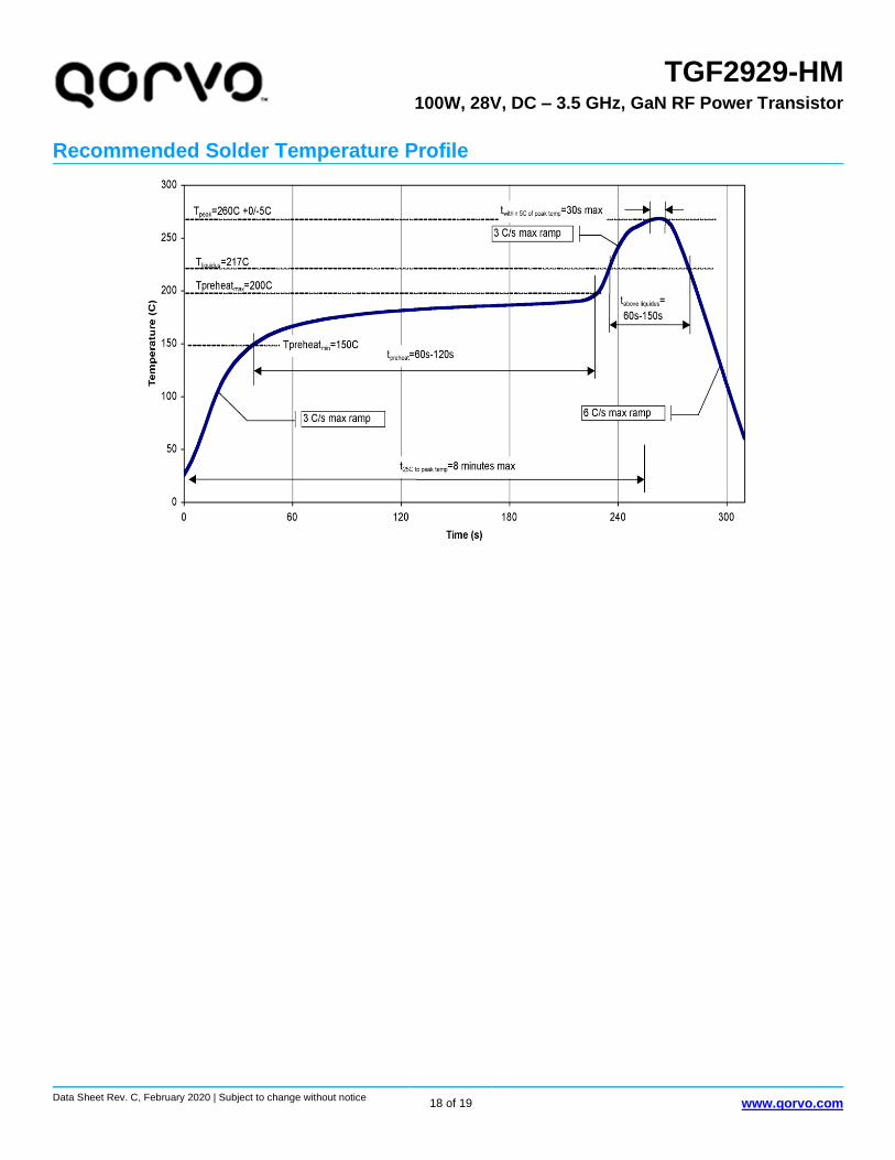
Recommended Solder Temperature Profile

TGF2929-HM 100W, 28V, DC – 3.5 GHz, GaN RF Power Transistor
Data Sheet Rev. C, February 2020 | Subject to change without notice
19 of 19 www.qorvo.com
Contact Information For the latest specifications, additional product information, worldwide sales and distribution locations:
Web: www.qorvo.com
Tel: 1-844-890-8163
Email: [email protected]
Important Notice The information contained herein is believed to be reliable; however, Qorvo makes no warranties regarding the information contained herein and assumes no responsibility or liability whatsoever for the use of the information contained herein. All information contained herein is subject to change without notice. Customers should obtain and verify the latest relevant information before placing orders for Qorvo products. The information contained herein or any use of such information does not grant, explicitly or implicitly, to any party any patent rights, licenses, or any other intellectual property rights, whether with regard to such information itself or anything described by such information. THIS INFORMATION DOES NOT CONSTITUTE A WARRANTY WITH RESPECT TO THE PRODUCTS DESCRIBED HEREIN, AND QORVO HEREBY DISCLAIMS ANY AND ALL WARRANTIES WITH RESPECT TO SUCH PRODUCTS WHETHER EXPRESS OR IMPLIED BY LAW, COURSE OF DEALING, COURSE OF PERFORMANCE, USAGE OF TRADE OR OTHERWISE, INCLUDING THE IMPLIED WARRANTIES OF MERCHANTABILITY AND FITNESS FOR A PARTICULAR PURPOSE.
Without limiting the generality of the foregoing, Qorvo products are not warranted or authorized for use as critical components in medical, life-saving, or life-sustaining applications, or other applications where a failure would reasonably be expected to cause severe personal injury or death.
Copyright 2020 © Qorvo, Inc. | Qorvo is a registered trademark of Qorvo, Inc.
Handling Precautions Parameter Rating Standard
Caution! ESD-Sensitive Device
ESD – Human Body Model (HBM) Class 1B ANSI/ESDA/JEDEC JS-001
ESD – Charged Device Model (CDM) Class C3 ANSI/ESDA/JEDEC JS-002
Solderability Compatible with both lead-free (260°C max. reflow temp.) and tin/lead (245°C max. reflow temp.) soldering processes.
Solder profiles available upon request.
Package lead plating is NiAu. Au thickness is 60 microinches.
RoHS Compliance This part is compliant with 2011/65/EU RoHS directive (Restrictions on the Use of Certain Hazardous Substances in Electrical and Electronic Equipment) as amended by Directive 2015/863/EU. This product also has the following attributes:
• Lead Free
• Halogen Free (Chlorine, Bromine) • Antimony Free
• TBBP-A (C15H12Br402) Free
• PFOS Free
• SVHC Free
Pb