testing high speed serial io interfaces based on spectral jitter decomposition · ·...
TRANSCRIPT

1
'HVLJQ&RQ�������
Testing High Speed Serial IO Interfaces Based on Spectral Jitter Decomposition
Rainer Plitschka, Agilent Technologies, Inc. E-mail: [email protected] Bernd Laquai, Agilent Technologies, Inc. E-mail: [email protected]

2
$EVWUDFW�This paper proposes a new method to verify the jitter performance by decomposition into its spectral components. The implementation for spectral jitter decomposition deploys the conventional real-time compare to expected data on ATE or BERT equipment. The key difference is a different sampling point location used for comparing. The spectral power density is calculated from the obtained error signal, yielding the jitter energy spectrum. By analyzing their spectral properties, the measurement results identify parasitic jitter sources that crosstalk into sensitive high-speed IO interfaces like PCI Express, S-ATA and XAUI. The paper shares experimental results and provides a mathematical description of the proposed method for an in-depth understanding.
���$XWKRU�V��%LRJUDSK\�Rainer Plitschka�is with Agilent Technologies since 1979. He worked in R&D as hardware engineer as well as within project management. In 1995 he joined marketing with functions in sales development and product marketing. Today his focus is set for applications needing parallel BER Testing. He holds a diploma in microwave technology from University Karlsruhe, Germany. Bernd Laquai received his Dipl.-Ing. Degree in Electrical Engineering from University of Stuttgart, Germany and started his professional career at the Research Institute for Microelectronics in Stuttgart (IMS) in 1987. In 1997 he joined Hewlett-Packard / Agilent and is now a member of the R&D team responsible for generating new test solutions on the 93000 ATE platform family particularly focused on high-speed interfacing.

3
,QWURGXFWLRQ�Massive parallel embedding of high-speed IO ports running at multiple Gigabits per second is certainly the most prevalent method used these days to match the lagging IO bandwidth of SOC-devices to the constantly growing performance of digital logic cores. However, crosstalk from millions of simultaneously switching digital transistors, that injects jitter into the sensitive analog high-speed IO ports is substantially eating up the timing margins of the sub-nanosecond bit intervals available for transmission. Therefore, managing the jitter is the toughest challenge to be successful with the new IO technology. IC-testers (ATE) as well as parallel Bit Error Rate Testers (BERTs) are readily available to stimulate the device under test with high-speed data and to compare the device response at-speed to expected data. This equipment is required to verify the mission mode functional behavior and to perform the measurement of critical parameters such as the Bit Error Rate (BER) and other traditional performance data to confirm the compliance with key standards or proprietary specifications. The traditional test approaches evolved from the early high-speed communication applications implemented in standalone devices using dedicated semiconductor materials such as Gallium-Arsenide or Silicon-Germanium. Devices of this kind easily consumed several Watts of power when they were running at multiple Gigabits per second, even for single channel IO. The former standard driven and costly measurement techniques were completely focused to singular long haul interconnects using optical fibers for transmission targeted for the high-end communication market. This situation has changed meanwhile. With CMOS structure sizes below 250nm, Gigabit transmission was feasible and quickly became a disruptive technology for chip-to-chip interconnects and backplanes in many electronic systems. It is no longer an optical fiber but regular PCBs with low cost FR4 material as dielectric that is used as a low-cost transmission medium, causing a noticeable loss in transmission performance. Highly complex CMOS designs are under development using hundreds of IO’s and operating far beyond a Gigabit per second. The high speed IO’s are no longer standalone but are massively embedded in parallel into large microprocessors, graphic chipsets, memory controllers, highly integrated switches or router devices. The loss in performance of the transmission medium as well as the high integration density had a significant impact on the required circuit design to still guarantee fault-free transmission. Sophisticated equalization was introduced to compensate the lossy behavior of the FR4 dielectric. Data rate matching techniques were introduced to compensate for rate differences up to 300ppm. New clocking schemes and coding techniques were developed to reduce electromagnetic interference. High effort was spent to reduce power and to make the embedded IO macrocells immune against switching noise as it is generated by today’s microprocessors. The test methodologies, however, couldn’t keep pace with the changes in circuit design. Jitter test methodology is still in its infancy. The mathematical models and measurement techniques for jitter are still as simple as in the past. Even though some awareness for the need of new test methodologies appeared, specific aspects such as jitter separation into different categories aren’t solved completely yet. Dedicated and different equipment is required to quantify the various jitter phenomena accordingly.

4
Debugging to eliminate jitter sources is a tedious and time-consuming job and jitter testing in production is a costly nightmare. A particularly difficult aspect for the designers of SOC-devices is that jitter induced by ground bounce and clock crosstalk can hardly be simulated with existing tools on the top level of a huge SOC design containing millions of transistors. Furthermore the leading-edge high-speed IO standards require the use of the most recent process technologies that often aren’t in a mature state yet and only leave minimum design margins. As a consequence, process variations significantly affect the analog performance of the high speed IO circuitry and achieving sufficient design robustness is a constantly moving target. Unpredictable jitter performance that requires a tedious and empirical tweaking over several design cycles is the result. Since the competitive pressure in the respective markets is high, a product often can’t wait to be fully optimized for its jitter performance and production starts while process variations still affect performance critically. Therefore it is crucial to quickly identify jitter issues in first silicon that affect the design robustness. This also makes an efficient jitter test methodology in early production inevitable to ensure appropriate product quality. Given this situation, test methodologies for both design verification as well as for production are required providing a cost-efficient and more problem specific analysis and test of the jitter phenomena. The new method presented in this paper exactly serves this purpose. Whereas existing techniques make use of statistical methods and destroy the frequency information contained in the jitter the method proposed in this paper preserves it and uses it for spectral decomposition. The obtained spectral characteristic of the jitter reveals exactly the information that allows immediate identification of the jitter sources. The method categorizes the jitter based on its frequency and makes a frequency selective measurement and test of jitter possible.

5
7KH�6SHFWUDO�-LWWHU�'HFRPSRVLWLRQ�0HWKRG� 7KH�2ULJLQ�RI�WKH�0HWKRG�Analog to digital conversion based on single bit conversion is commonly used in audio applications. High accuracy and linearity can be achieved using a simple and low-cost implementation of the so-called bit stream technology (sigma-delta converters et al.). The generic concept that makes the A/D conversion with a single 1-bit comparator possible is based on adding noise to the analog signal before it is digitized (fig. 1).
Fig. 1: Single bit conversion principle The single bit conversion principle can be understood easily when we imagine the analog input signal being offset arbitrarily by the noise relative to the comparator threshold. This means that superimposing noise, conceptually moves the input signal up and down across the fixed compare threshold and therefore allows digitizing of different signal levels in the analog input signal. The result is a binary bit stream that contains the analog signal information in terms of a binary bit density. Extraction of the analog signal from the digital bit stream representation is simply achieved by low-pass or narrow band-pass filtering. The impact of the superimposed noise and the extraction of the analog input signal from the binary coded bit stream are described best in the frequency domain. The superimposed noise has a high bandwidth compared to the analog input signal, and the noise energy is spread over the whole bandwidth. This means that only a small amount of energy falls in the frequency band consumed by the input signal. Therefore the spectral energy of the analog input signal is minimally distorted by the noise energy and simple frequency selective filtering eliminates the majority of the noise energy outside the band of interest when retrieving the analog signal from its binary representation. In a sigma-delta converter the noise is obtained by feeding back the quantization noise that occurs as a result of the 1 bit comparison. Extremely high accuracy is obtained by additional shaping of noise. The noise in the frequency band of interest is suppressed before adding the high frequency noise.

6
The bit stream single bit A/D conversion principle is commonly used for conversion and processing of signal amplitudes. However, it can also be leveraged to the timing domain, where it can be used advantageously to represent and post-process the jitter modulation waveform contained in a high-speed data signal using a single comparator. In timing domain application of the bit stream conversion technology, the comparator does not compare for amplitudes but for the phase of bit transitions in an incoming data signal. Leveraging this principle leads to the proposed method for the spectral jitter decomposition and analysis. )XQGDPHQWDOV�RI�WKH�1HZ�3URSRVHG�0HWKRG�When a conventional bit error rate measurement is performed on a data signal, the goal is to find a threshold and a sampling point for comparison such that the BER is zero or at least minimized. Typically this sweet spot is within the center of the data eye. With the proposed method, however, we offset the sampling point into the crossover section of the data eye where the compare of captured versus expected data yields a bit error signal. A conventional bit error rate tester or automated test equipment (ATE) can be used to implement the method. Figure 2 shows a schematic of the basic principle. This example assumes a mixture of random and sinusoidal jitter is injected into the stream of data. The Error Signal is the result of the comparison between the incoming data and the expected data. So this is a real-time digitized bit stream coded with ‘0’ for match and ‘1’ for difference between incoming data and expected data. This Error Signal gained from sampling at the crossover is no longer a simple Pass/Fail result; it contains the frequency information of the actual jitter. Just from looking at the jitter histogram no conclusion can be made on the frequency of the jitter because forming a histogram basically destroys any frequency information. In the example of Figure 2 the Error Signal sampled and compared in the crossover point shows up with a periodic modulation of the error density. During the positive period of the sinusoidal component the error density is increased, since the short-term mean of the random jitter portion is offset by the sinusoidal component, which increases the eye closure. During the negative portion of the sinusoidal component errors are also generated, but with smaller density than during the positive portion. Therefore the modulation of the error density in the error signal reflects the spectral properties of the jitter modulation. The period of the sinusoidal jitter gets transferred into the Error Signal and can be extracted by statistical methods such as the calculation of the autocorrelation function or the calculation of the spectral density of the signal. The Error Signal is an at-speed signal. But there is no need to process the Error Signal in real-time. BERT and ATE equipment provide memory to store the obtained Error Signal. So the Digital Signal Processing (DSP) Tools will be applied after recording the Error Signal for a certain length.

7
Fig. 2: Generation of the error signal for the proposed method (schematically)

8
7KH�9LVXDOL]DWLRQ�RI�WKH�6SHFWUDO�'HFRPSRVLWLRQ� Figure 3 represents the spectral density as obtained from the Error Signal; it shows Spectral Energy over Frequency. In the generic case of mixed random and deterministic periodic jitter the Spectral Decomposition can show 3 different categories of jitter: a) A broadband jitter spectrum caused by the random jitter and shaped by the PLL loop filter of the device under test revealing important information on the PLL bandwidth (indicated by the corner frequency). b) One or more peaks of deterministic periodic jitter of lower frequency than the corner frequency of the PLL loop filter that can be tracked by the PLL of the device, so-called “in-band jitter” c) One or more peaks of deterministic periodic jitter of higher frequency than the corner frequency of the PLL loop filter that can not be tracked by the PLL of the device, so-called “out-of-band jitter” The fact that the spectral power density of the random portion gets distributed over many frequencies while the spectral power of the periodic portions stays concentrated in discrete lines significantly enhances the detection of spurious periodic jitter deeply buried in random jitter. Thus even smallest sources of periodic and deterministic jitter can be identified and compared to a limit.
Fig. 3: Spectral density of the error signal
9
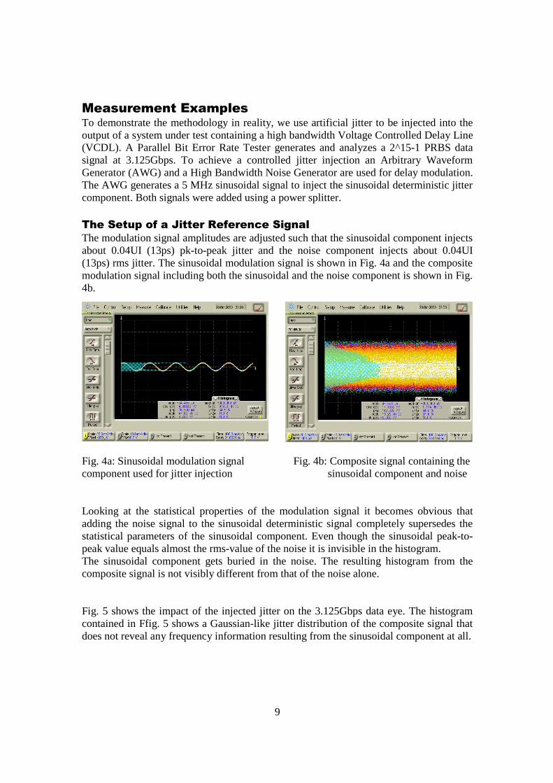
0HDVXUHPHQW�([DPSOHV�To demonstrate the methodology in reality, we use artificial jitter to be injected into the output of a system under test containing a high bandwidth Voltage Controlled Delay Line (VCDL). A Parallel Bit Error Rate Tester generates and analyzes a 2^15-1 PRBS data signal at 3.125Gbps. To achieve a controlled jitter injection an Arbitrary Waveform Generator (AWG) and a High Bandwidth Noise Generator are used for delay modulation. The AWG generates a 5 MHz sinusoidal signal to inject the sinusoidal deterministic jitter component. Both signals were added using a power splitter. 7KH�6HWXS�RI�D�-LWWHU�5HIHUHQFH�6LJQDO� The modulation signal amplitudes are adjusted such that the sinusoidal component injects about 0.04UI (13ps) pk-to-peak jitter and the noise component injects about 0.04UI (13ps) rms jitter. The sinusoidal modulation signal is shown in Fig. 4a and the composite modulation signal including both the sinusoidal and the noise component is shown in Fig. 4b.
Fig. 4a: Sinusoidal modulation signal Fig. 4b: Composite signal containing the component used for jitter injection sinusoidal component and noise Looking at the statistical properties of the modulation signal it becomes obvious that adding the noise signal to the sinusoidal deterministic signal completely supersedes the statistical parameters of the sinusoidal component. Even though the sinusoidal peak-to-peak value equals almost the rms-value of the noise it is invisible in the histogram. The sinusoidal component gets buried in the noise. The resulting histogram from the composite signal is not visibly different from that of the noise alone. Fig. 5 shows the impact of the injected jitter on the 3.125Gbps data eye. The histogram contained in Ffig. 5 shows a Gaussian-like jitter distribution of the composite signal that does not reveal any frequency information resulting from the sinusoidal component at all.

10
Fig. 5: Data eye at 3.125Gbps with induced random and sinusoidal jitter 7KH�&DOLEUDWLRQ�RI�WKH�-LWWHU�5HIHUHQFH�6LJQDO� With the jitter injected into the data, the high-speed output signal is captured real-time with the error analyzer of a Parallel Bit Error Tester and compared to the expected data. By sweeping the sample point the a Bathtub Curve is recorded (Fig. 6).
Fig. 6: Bathtub Curve for no jitter, sinusoidal, random noise and combined modulation
No jitter Sinusoidal Random noise Sine & Noise
11
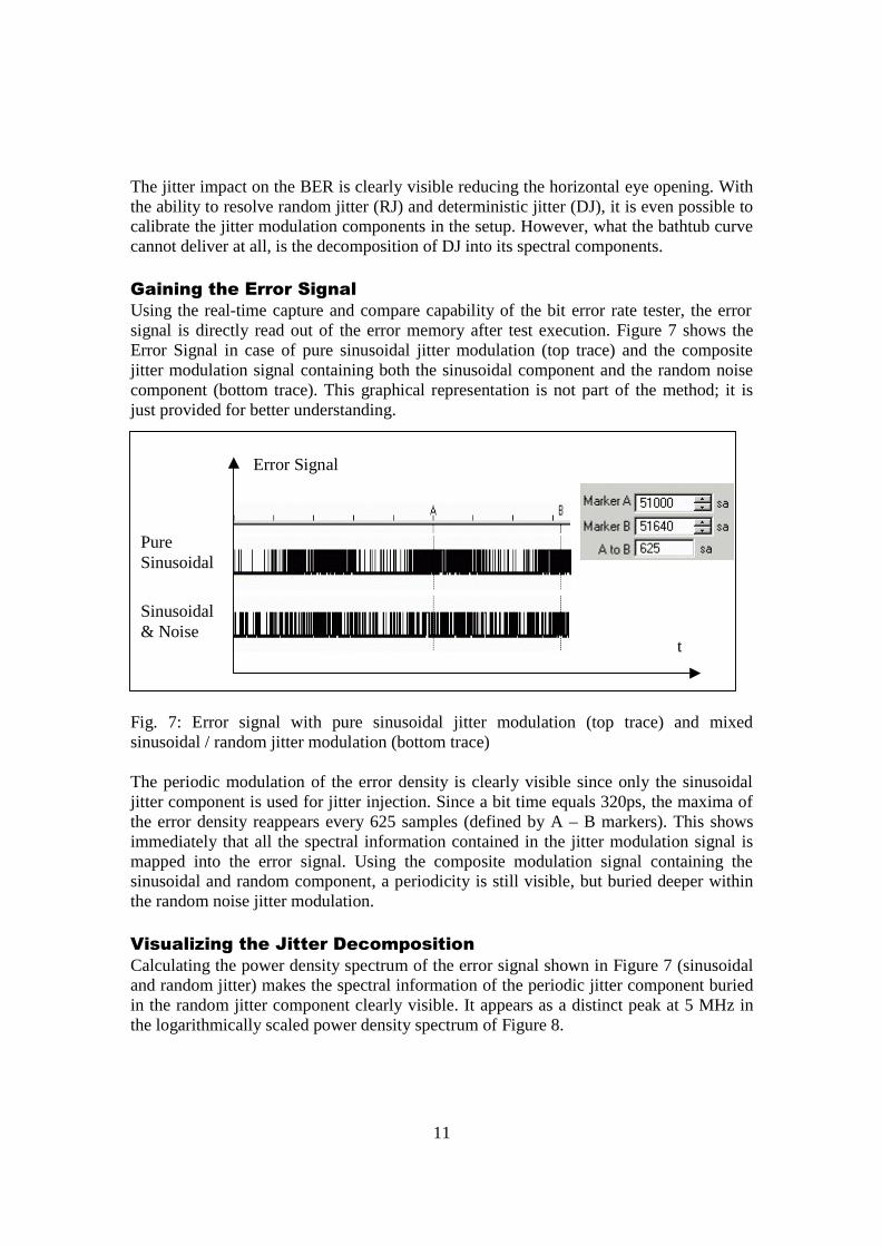
The jitter impact on the BER is clearly visible reducing the horizontal eye opening. With the ability to resolve random jitter (RJ) and deterministic jitter (DJ), it is even possible to calibrate the jitter modulation components in the setup. However, what the bathtub curve cannot deliver at all, is the decomposition of DJ into its spectral components. *DLQLQJ�WKH�(UURU�6LJQDO Using the real-time capture and compare capability of the bit error rate tester, the error signal is directly read out of the error memory after test execution. Figure 7 shows the Error Signal in case of pure sinusoidal jitter modulation (top trace) and the composite jitter modulation signal containing both the sinusoidal component and the random noise component (bottom trace). This graphical representation is not part of the method; it is just provided for better understanding.
Fig. 7: Error signal with pure sinusoidal jitter modulation (top trace) and mixed sinusoidal / random jitter modulation (bottom trace) The periodic modulation of the error density is clearly visible since only the sinusoidal jitter component is used for jitter injection. Since a bit time equals 320ps, the maxima of the error density reappears every 625 samples (defined by A – B markers). This shows immediately that all the spectral information contained in the jitter modulation signal is mapped into the error signal. Using the composite modulation signal containing the sinusoidal and random component, a periodicity is still visible, but buried deeper within the random noise jitter modulation. 9LVXDOL]LQJ�WKH�-LWWHU�'HFRPSRVLWLRQ Calculating the power density spectrum of the error signal shown in Figure 7 (sinusoidal and random jitter) makes the spectral information of the periodic jitter component buried in the random jitter component clearly visible. It appears as a distinct peak at 5 MHz in the logarithmically scaled power density spectrum of Figure 8.
Error Signal
t
Pure Sinusoidal
Sinusoidal & Noise

12
Fig. 8 Spectral power density of the recorded error signal from fig. 7 (bottom) 5HVXOWV�IURP�D�;$8,�'HYLFH
Fig. 9a: Jitter transfer test of a 3.125Gbps XAUI SerDes using random jitter injection into the reference clock and using the spectral decomposition method The proposed method allows the identification and analysis of the bandwidth of a random jitter as it passes through a loop filter of a PLL. Even though the random jitter spreads its
- Sine & Noise - Random noise
Peak at 5 MHz

13
spectral energy over a certain bandwidth, the logarithmic display of the power density spectrum allows the identification of the bandwidth of random jitter as well as its roll-off character. This approach was used to verify the PLL jitter transfer characteristic of a 3.125Gbps SerDes. Broadband noise injects a random jitter modulation into the 156MHz reference clock of a XAUI SerDes. The TX jitter output is investigated with the spectral decomposition method described above. We can clearly identify the shaping of the jitter spectrum by the PLL loop filter (Fig. 9a). Since we use broadband noise instead of a swept sinusoidal single tone to measure the jitter transfer we are able to perform the analysis in one shot. The plot of Figure 9a uses a prototype implementation of the measuring framework. The graph shows directly the spectral power density as calculated from the error signal. 5HVXOWV�IURP�D�3&,�([SUHVV�'HYLFH�
�Fig 9b: Spectral Decomposition Result from a PCI Express TX Device in Compliance Mode, Roll Off and Crosstalk from a 187.5MHz int. Clock� Another example is taken from a real PCI Express TX circuit running in Compliance Mode. For this measurement the TX output signal is fed into a Clock-Data-Recovery Circuit (CDR) to extract a clock from the data signal, as PCI Express does not provide a clock at data rate. Using a CDR for jitter measurements is normally a good idea, as the low frequency jitter components, which do not harm when operating, will be eliminated from the readings. In this case the Device under Test shows a crosstalk from an internal Clock running at 187,5 MHz. This information is extremely helpful for the designer, as he is immediately able to locate the problem area.
- Roll Off - Clock Crosstalk

14
&RQFOXVLRQ�IURP�WKH�0HDVXUHPHQW�([DPSOHV�The measurements clearly show that a regular capture and compare of a data stream with the compare strobe positioned at the bit interval boundary transfers the spectral information contained in the jitter completely into the binary error signal. Therefore the simple calculation of the power density spectrum from the error signal allows the spectral decomposition and analysis of the jitter and allows the spectral identification of parasitic jitter sources. This aspect can be used efficiently for testing. Typically jitter is the result of crosstalk of clocks from the digital cores into sensitive Phase Locked Loops (PLL’s) or Delay Locked Loops (DLL’s). The main crosstalk mechanisms are directly coupling micro-fields or crosstalk by ground-bounce and charge injection into a common substrate. Jitter may also be the result of bandwidth limitations that come along with a non-linear phase characteristic causing the pattern dependent offset of the transitions in a bit stream. During the test of devices we normally can assume that the test patterns are repeated periodically and therefore the pattern dependent jitter appears as periodic jitter during test in the same way as the clock induced jitter. Therefore both clock crosstalk and pattern dependent jitter concentrate their energy into discrete spectral lines that are clearly visible in the jitter spectrum with significant distance to the noise floor generated by the random jitter. A difference, however, exists in terms of jitter frequencies. Whereas jitter caused by clocks from the digital core appears at several hundreds of MHz with a single or few components, the data dependent jitter is very high frequency in nature and, due to run length variations in the pattern, appears as a bunch of parasitic spectral components. This spectral behavior can be used advantageously to separate the jitter sources with the proposed method. A characteristic result from a spectral jitter decomposition with the method as shown is the appearance of individual distinct jitter peaks or a group of jitter peaks in the case of a defective device. It is therefore possible to not only identify respective frequencies of defect inducing jitter sources but also to define frequency selective pass/fail criteria to efficiently screen devices for the appearance of those separated jitter defects. In addition to a frequency selective jitter screening, a more global test using a pass/fail mask in the jitter spectrum is possible to test for unexpected jitter sources. Finally we also conclude that even a jitter transfer test is possible with the proposed method. The intentional injection of either sinusoidal, multi-tone or even broadband noise signals into the reference clock of a device under test can be used to characterize the jitter transfer characteristic of its PLL’s and DLL’s and to create specific test criteria for extracted parameters such as the loop bandwidth.
4XDQWLILFDWLRQ�RI�6SHFWUDO�-LWWHU�&RPSRQHQWV�The method as described above allows the spectral decomposition of jitter contained in a data signal. The most important aspect of the decomposition is certainly the identification of jitter sources from its associated frequencies in the spectrum. However, there might also be an interest to quantify the individual spectral jitter components for their energy even though the spectral power density is the result of a non-trivial mapping of the jitter modulation into the binary error density. The following section shows that such a

15
quantization of the spectral jitter components is possible and it derives the required mathematical relationships to do an analytical description of the proposed method. 2EVHUYDWLRQV�LQ�WKH�OHYHO�GRPDLQ�The final goal of the proposed method for spectral jitter decomposition is to use the algorithm in the time (phase) domain of the signal. However, the explanation of the basics is easier with an analogy in the signal level domain. For the following we will assume that uniformly distributed white noise is added to an analog signal s(t). When we use a 1 bit clocked comparator to sample the noisy signal we get a binary random bit stream b(t) that randomly toggles between the logic values and the analog signal modulates the density of the logic values. Thus, the output of the comparator represents the analog signal in terms of an error bit density (fig 10).
Fig. 10: Digitizing of an analog sinusoidal signal using additive noise and a bit stream modulation technique To investigate the role of the noise for obtaining a bit density encoded binary representation of the signal we will initially use uniformly distributed noise where the probability distribution function (PDF) is constant with a value of 1/(2α) across the level range from -α to +α. The respective cumulative distribution function (CDF) then has a triangular shape (fig. 11), the mean is zero and the variance is σ2 = 1/3*α2. In the case of α=1 the PDF p(x) and CDF F(x) are given by:
(1)

16
(2) The case of α≠1 can be easily derived considering the fact that if a random variable X is distributed with F(x) and is transformed it into another random variable Y according to Y=aX+b then Y is distributed with F((y-b)/a).
Fig. 11: Probability functions of the uniformly distributed noise Assigning the values 0 and 1 to the logic levels and using uniformly distributed noise means that for an analog input level s(t0)=x with x below -α the output b(t) would be constantly 0 and for an input greater than +α the output would be constantly 1. The voltages in between are linearly mapped to a binary random signal such that the bit density d(t) follows a straight line according to:
(3) This density characteristic is equivalent to the CDF of the additive noise. In order to get a more balanced binary output signal it is advantageous to assign the values –1 and +1 to the logic levels. In this case we have to map the previous CDF into the range -1 to +1

17
requiring the multiplication of the previous result with a factor of 2 and to offset it by –1. Therefore, the mapping of an analog value at the input to the output density can be described with:
(4) The result is shown graphically in fig. 12.
Fig. 12: Mapping of an analog input level into a bit density for uniformly distributed noise and logic levels –1 and +1. As a conclusion the uniformly distributed noise superimposed on the analog signal allows a linear mapping into a binary random signal with a bit density proportional to the analog signal level:
(5) The scaling (gain) factor m of the mapping represented by the steepness of the mapping characteristic is linked to the standard deviation σ of the noise:
(6)

18
In the more common case of Gaussian random noise we get the following result for the density function d(x) with similar considerations:
(7) where erf(x) is the tabulated error function. Fig. 13 shows the bit density mapping characteristic graphically.
Fig. 13: Mapping of an analog input level into a bit density for Gaussian noise From the characteristic of the error function erf(x) we can conclude that in the case of Gaussian random noise the mapping is linear in the range of -σ to +σ. Beyond this range we get a nonlinear compression effect. However, the knowledge of the mapping characteristic allows the compensation of the nonlinear compression by simply calculating the inverse mapping on the result, if necessary. For small signals around the zero level we get a scaling factor m that is the derivative at the point zero:
(8) When we investigate the resulting binary random bit signal b(t) in the frequency domain we observe that the spectral energy of the transferred noise is spread over the whole spectrum (assuming an input of white noise with a bandwidth BW) in the same way as for the noise modulation signal.

19
The power density spectrum Bbb(f) describes the energy and is defined either as the Fourier transform of the autocorrelation function of b(t) or by the squared magnitude spectrum of B(f, T) where B(f, T) is the finite Fourier transform of b(t) in a given finite time interval T with T being sufficiently large (see also /2/):
(9) Since the discrete Fourier transform (DFT) already assumes a periodically repeated finite time interval, the use of a DFT or FFT algorithm is particularly suited to calculate the sampled version of Bbb(f) with an accuracy that improves the more samples are taken. In the presence of the noise only we can assume that the sum of all spectral components in the power density spectrum yields the noise energy that is equal to the variance (a noise signal that contains no DC component is assumed):
(10) Therefore the noise floor in the power density spectrum generated by the noise only is:
(11) Since we assumed the noise to be white until the given bandwidth it appears as a constant noise floor. When we keep σ constant, the noise floor becomes smaller as the bandwidth increases. The spectral components of the analog input signal are linearly mapped for input ranges between -σ and +σ according to the bit density mapping described above. In case of a sinusoidal analog signal, this means that its signal energy appears as a spike in the power density spectrum Bbb(f) with all the energy concentrated into a single spectral component.

20
It is therefore clearly visible in the power density spectrum of the bit density function. In case the amplitude of a sinusoidal signal is A, the respective density amplitude maps to:
(12) The respective energy of the signal appears as a peak with the energy E=1/π·(A/σ)2 at the respective signal frequency. Fig. 14 shows the respective power spectrum calculated from the bit density signal for a sinusoidal analog input signal, uniformly distributed white noise with standard deviation σ, mean µ=0 and logic levels –1 and +1.
Fig. 14: Power density spectrum of the binary random compare signal 7UDQVIHU�RI�WKH�UHVXOWV�WR�WKH�WLPH�SKDVH�GRPDLQ�In the signal level domain we compared levels to a fixed level threshold of zero and derived the mapping into a bit density function. This intermediate result can now be transferred into the time or phase domain. When we focus our investigations in the time domain to a single bit interval derived from a fixed reference clock, we can associate a phase to the timing events in a single bit interval. The timing events are formed when bit levels change and the level threshold crossings occur. A transfer of the level domain approach into the phase domain therefore means a comparison of the phase offset of a bit level transition to the boundary (phase=0) of the individual bit interval (see fig 15).

21
Fig. 15: Sampling data to compare for the phase offset In order to do a binary comparison for the phase offset, it must be decided whether the transition occurred before or after the sample strobe that is positioned at the bit interval boundary (typically 0.5UI apart of the center of the data eye). This decision is now equivalent to the level decision in the level domain using a level compare threshold. However, the decision result is now obtained by comparing the sampled bit value to the expected data at the bit interval boundary. In the case the transition from bit n to bit n+1 occurs later than the start of the bit interval n+1, the bit n is sampled. The comparison reports no error. In the case the transition from bit n to bit n+1 occurs earlier than the start of the bit interval n+1 the bit n+1 is sampled. If the bit n+1 is different from the bit n the comparison results in an error. Since two adjacent bits can be either equal or different, the error occurs only with a probability of 0.5 in this case. Therefore the deviation from the average error probability of 0.5 indicates the decision result. In case there is no transition no comparison takes place and no result will be generated from that bit. When we investigate the mapping characteristic of the jitter modulation into the bit error density we clearly observe that the shape follows the CDF of the noise as in the case of the level comparison except for a different scaling factor and offset. This difference can be explained by the fact that an offset of less than –1UI or an offset of more than +2UI yields an error probability of 0.5 in case of truly random data and provided the duration of adjacent bits is still close to nominal (low jitter frequency). We obtain the asymptotic approach towards the value of 0 because the two adjacent bits can either be equal or different with the same probability 0.5. Assigning the levels of +1 and -1 for error / no-error yields the average value of 0. On the other hand it is pretty obvious that when the transition is offset to the center of bit n+1 and we actually compare to the expected data of bit n we should reach a minimum error density of 0. Since we assigned the value of –1 for no-error the density shows up with a value close to -1 in the center of the data eye. From the left side and the right side we see a roll-off according to the error function as a result of the Gaussian noise we used.
22
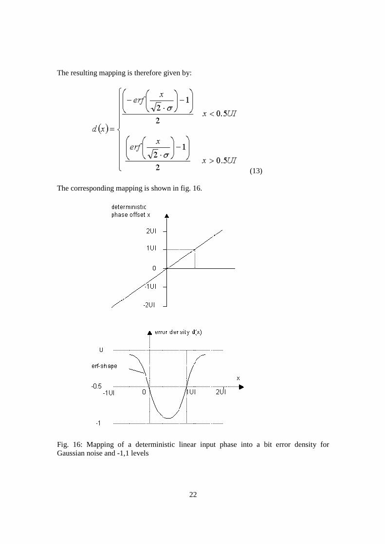
The resulting mapping is therefore given by:
(13) The corresponding mapping is shown in fig. 16.
Fig. 16: Mapping of a deterministic linear input phase into a bit error density for Gaussian noise and -1,1 levels

23
As a result we can define the mapping factor m for the sample strobe positioned at the phase offset 0:
(14) For the sample strobe positioned at the phase offset 1UI compared to the end of the next bit interval (this indicates the right boundary or the end of the bit interval of bit n+1), and the mapping factor is:
(15) Similar to the level domain we are now able to also determine the spectral energy of the error density signal of a sinusoidal jitter component with amplitude A from the mapping factor m for the linear mapping range. It will be mapped to a peak height in the power density spectrum of:
(16) The boundary conditions for this result are: the amplitude A of the sinusoidal jitter component is smaller than 1σ of the random Gaussian jitter, the Gaussian random jitter is assumed to have a bandwidth significantly higher than the frequencies of the spectral components of interest and the assignment of the logic values are –1 for no error 1 for an error as a result of the compare. 5HVXOWV�RI�WKH�WKHRUHWLFDO�LQYHVWLJDWLRQV�The theoretical investigation related to the quantification of the results obtained with the proposed method for spectral jitter decomposition helps us understand some key properties of the method. First of all it shows that the statistical properties of the noise described by the CDF determines the linearity of the mapping. Since the Gaussian CDF is linear in the range from -σ to +σ the presence of Gaussian random noise constraints the direct linear amplitude mapping of the deterministic signal to peak amplitudes less than -σ to +σ. Exceeding this range will lead to non-linear distortions, resulting in harmonics that appear in the power density spectrum. However, when the CDF is known, a linearization is possible with a post-processing using the inverse characteristic of the Gaussian CDF. Another result is that the mapping factor m can be easily determined. When A is much smaller than σ, the rms-value of the composite signal will not be affected by the sinusoidal component. In order to determine m it is therefore only required to measure

24
the rms-value of the composite jitter. The theoretical results also indicate that the mapping factor becomes larger as the rms-value of the random jitter component decreases. This means that small amounts of deterministic jitter can be “amplified” using random jitter that is as small as possible. In most cases the device intrinsic random jitter is sufficient for this purpose. If the device intrinsic random jitter is too small to fulfill the constraint of linear mapping, it can be easily be added using random data and an interconnect cable or loadboard trace, connecting it to the measurement equipment that causes high frequency data dependent jitter. Since data dependent jitter depends on a few previous bits only the injected frequencies are in the range of the baud frequency. In this case random test patterns cause many different randomly varying run lengths resulting in a Gaussian distribution of the injected data dependent jitter that gets superimposed on the deterministic jitter generated by the device under test. Adding the data dependent jitter makes it possible to linearly map a periodic jitter component at lower frequency. In case the frequency range of interest is below the loop bandwidth of the PLL, a further option is the additional injection of random jitter into a reference clock input of the device under test. In this case, the PLL transfers the random jitter into the circuitry under investigation and this allows a linear mapping of periodic jitter components generated in the device. We can also use the theoretical results to verify the previous experimental result. In the experiment the injected sinusoidal jitter peak-to-peak amplitude was about equal to 1σ of the random jitter. Therefore the sinusoidal peak amplitude is half of it. According to formula (16) a ratio of 0.5 yields a peak height of 0.02 rad2/Hz in the power spectrum. The experimental result therefore matches the theoretical result.
�6XPPDU\�DQG�&RQFOXVLRQ�With the method described above we introduced a new approach for jitter testing. We were able to prove that it is possible to extract jitter from high-speed data signals and decompose it into its spectral components using already existing equipment such as ATE and BERT equipment. The approach of using the spectral view on the jitter not only allows immediate identification of jitter sources for debugging but also allows a frequency selective testing of jitter for production purposes. We explained the new methodology conceptually, verified it with experiments and gave a detailed mathematical description. The method is derived from proven sigma-delta single bit conversion technology that is used for years now in audio applications with highest accuracy. The basic idea is to leverage the single bit conversion technique from the level domain into the phase domain. It can be seen that the effort to implement the method on real-time capture and compare equipment is minimal. With existing equipment the setup for comparing the device output data to the expected data has to be changed simply such that the compare threshold occurs in the crossover of the data transitions. We were able to show that the resulting error density signal contains all spectral information of the jitter. Therefore it is only required to calculate the spectral power density from the error signal to visualize the spectral properties.

25
With this method we were able not only to extract the frequency information of parasitic jitter components but also to quantify the spectral jitter components with respect to their jitter energy. In order to achieve a linear mapping of spectral jitter energies into the error density signal, sufficient random jitter is required in addition to the periodic deterministic jitter components of interest. However, given a mixture of random and periodic jitter, we were also able to prove that the method is able to extract the deterministic portion even though it is deeply buried in the random jitter. It is therefore possible to identify even the smallest deterministic jitter sources. Finally we also succeeded to use the method for analyzing phase regulation circuitry such as PLL’s and DLL’s for their jitter transfer characteristic. Jitter bandwidth and roll-off characteristic can be determined by evaluating the spectral shaping of white, random input jitter at the circuit output. Overall we believe the new test methodology is a significant contribution to enable the design community to quickly verify and improve the jitter performance of highly complex SOC silicon by using existing ATE or BERT equipment and to help the test engineer to ensure product quality with efficient production testing that includes jitter. /LWHUDWXUH�/1/ A. Papoulis: Probability, Random Variables and Stochastic Processes, McGraw Hill 1965 /2/ J. S. Bendat: A. G. Piersol, Random Data, John Whiley&Sons, 1986 /3/ Yi Cai, Bernd Laquai, Kent Luehman: Jitter Testing for Gigabit Serial Communication Transceivers, IEEE Design and Test of Computers, Jan-Feb 2002 /4/ Bernd Laquai, Yi Cai: Testing Gigabit Multilane SerDes Interfaces with Passive Jitter Injection Filters, IEEE Proc. of the International Test Conference 2001 /5/ T.J. Yamaguchi, M. Soma, M. Ishida, H. Musha, L. Marlasie: A New Method for Testing Jitter Tolerance of SerDes Devices Using Sinusoidal Jitter, IEEE Proc. of the International Test Conference 2002 /6/ J. Wilstrup: A Method of Serial Data Jitter Analysis Using One-Shot Time Interval Measurements, IEEE Proc. of the International Test Conference 1998 /7/ National Committee for Information Technology Standardization (NCITS) T11.2/Project 1230-DT “Fibre Channel – Methodologies for Jitter and Signal Quality Specification” Rev. 5.0, February 21, 2002 /8/ Jitter Analysis Techniques for High Data Rates, Application Note 1432, Agilent Technologies, 5988-8425EN, February 1, 2003