test rei'ort no. 22146-l for lk39f1 s/n u-l ... . nasa -22 , '., i., b-i* cr 141858 c. 1...
TRANSCRIPT

l .
N A S A - 2 2 , '., I., b- i * C R
1 4 1 8 5 8 c. 1
T E S T R E I'O R T N O . 2 2 146 - l
F O R
L K 3 9 F 1 S /N U-l. I N F R A R E D D E T E C 'X R
F O R
N A S A
H m e y w e I L Inc. Rac i i8 t i .m C e n te r
7 . Fo r bes R o a d Lex ing t rn , Mzssochuse t ts 0 2 1 7 3
https://ntrs.nasa.gov/search.jsp?R=19750017636 2019-03-19T13:19:18+00:00Z

.
.
.
i t
TEST REPORT NO. 22146-l PAGE 2 OF 1E TECH LIBRARY K&F& NM
llllllln llllll~ lllllll~ llllll~ lll~Il Ollb27l,i'
TABLE OF CONTENTS
SECTION
1.0 INTRODUCTION
2.0 DESCRIPTION OF DETECTOR
3.OA PERFOR-MNCE TABLE
3.OB GRAPHS OF TEST RESULTS
4.0 COhQITIONS OF MEASUREMENT
5.0 DETECTOR READOUT CIRCUITRY
6.0
7.0
HANDLING AND USE PRECAUTIONS - ANPLIFIER OPERATING INSTRUCTIONS
NOTE : PLEASE READ HANDLING AND USE PRECAUTiONS BEFORE USING THIS DETECTOR.

TEST REPORT NO. 22146-1 PAGE 3 OF 18
1.0 INTR&UCTION.
The multilayered (hg,Cd)Te detecto'? is sensitive to three infrared bands. Nominal cut-off wavelengths for each band arc as follows:
Channel 1 - 3 microns Channel 2 - 6 microns Channel 3 - 11 microns:
'The multilayered detector iS mounted in a Honeyweli 1x39 glass dewar. Accompanying the detector/dewar asstmbly is c 'tree-channel preamplifier package capable of switching each detector to the single channel input of the HRB Singer Reconfax IV Mark IV IrZrared Scanner.
-_.

-‘EST REPORT NO. 22146-1
-IPA 22146
XNTRACT NO. NAS9-14180
TEST REPORT NO. 22146-l PAGE 4 OF 18 1
(DEVICE) LK39Fl
CUSTOMER NASA/Johnson Space Center
2.0 DESCRIPTION OF DETECTOR
HRC Identification Number Type of Detector Date of Manufacture Window Material
Element -II
I.ength Width Area Distance to Window Field of View Liquid Nitrogen Hold Time (No&ml)
(S/N) U-l
50572S43D2 _Photoconductive (Hg,Cd)Te April, 1975 _Irtran II
.49
.s3
.26 4-8
40.0 _ 8.0
MM MM MM2 MN I)eotees - - Hours
. . -. - “_.. - _ -- u

TEST REPORT NO. 22146-1 PAGE 5 OF 18
3.0 PERFORMANCE TABLE .; .
A cut-off 300'K 77'K Optirmlm
Bias D* [1010] C%mneL (rlicrons) R[qj R[zz] [ma] AP
(1 KHZ) I) (10 KHz) .'R$12 wzl -- .-
1 2.9 1680 707 1 29 48 436,000
2 6.0 76 43 8 2.14 4.48 ' 872
3 11.4 20 1 33 8 2.24 I 2.66 944

1 ,o I 0.9
Q.8
0.7
0.6 I
0.5
, 014
! 0.3
0.2 I
O.?
I
i ~- TEST REPORT NO. 22140-I ;
:, PAGE 6 OF 18 :
a
I I,9 2.0 3.0 4.0 5.3 6.0 7.0. 8.0 9.9 10.0 11.0 12.0 .
.A (h4krons) .
RUATIM FfSPOME VS WAVELENGTH FOR THE 3-CHANNEL DETECTOR

w,_ . . , . . , , . I . . . , -
T E S T I& P O R T N O . 2 2 1 4 ;~ 1 5 P A G E 7 O F 1 8
R E L A T IV E S IG N A L V S . F R E Q :'E N C Y cl-!!xx 1
2 3 4 5 4 7 1 9 1 2 3 4 5 6 7 8 9 1 2 3 4 5 6 7 8 9 1 2 3 4 s 6 7 0 9 1 - -
i
.

1 Y 8 7 b .
I .
4
4
3
lo3 104 105
FREQUBXCY (hz)

NOISE VS. FREQUENCY TEST REPORT NO. 22146-1 18
C~4NNEL 1 PAGE 9 OF
1 2 3 4 s c 7891 1 2 a 4 5 6?59 I 2 3 4 44769
I 2 I . 44749
\ 100 :
7+-k- . . . . . . . , . . . . . ..--.. _.. .
-1’ ..’ 4
y .“_ _. -Tt- --7- .:
--i- -. i“ -f- . . . . . . . .
.:. .--_c ,G& . ‘:!
xIii7 xszt:: --L- . -7” . I -. :. --
.: p -4,;;
loL 10J lo4 lo5
FREQUENCY (Hz)
. , ,. . : . . . . ._ .,_. .I. .--

NOISE VS. FREQUENCY TEST REPORT 10. 22146-l CHANNELL PAGE 10 OF 18
1 2 3 4 5 b7aQl I 2 3 4 5 b789
1 2 3 4 5 6789 1 2 3 4 56759
1 2 J 4 5 b789.
1 9 8 .: 7 . . 1.. ._ 5 ,_..
4. .
J: f- Lil 1. :_ : : : .:.; i .::
: : : 3 . -: . .
! .l.-
;!- 2: :. .‘. : i ; :, -. - . - . . 4
f . .T
: *.
i
:
._* .
I/
ie
-’
. . ;. . I ”
I
: : . .
. -
. -
_.
~
I .-
: ; : :
. .
5
-”
I “I.
1
--
,I ‘1
t
IlO4 FREQUCNCY (Hz)
10 3

I 1
NOISE VS.,FREQUENCY TEST REPORT NO. 22146-l CHANNEL 3 PAGE 110F 18
) 2 3 4 5 6 7**: I 2 3 4 5 1783
1 - 34 54;u9 I 2 3 4 5 6169
1 2 3 4 5 6769
-e.-. - ' j-f-+--- A... l--.. --.
.F#++-
.'3,.l' -- .- ----:. +++++++++ -_. . . I L"Y+~, ;y - 1 e--j t- 1-- ,,. - -7-i _ ? k-Pu4
--I- -+.T, . 'I
..y-.p- . . . ..- . . ..,_ - I 4 -!-J-.1- .i- 14.A .-e,,.., .&...I
.!..- ..“I
’
!-.i:/?di.
*_ ..^ :
‘ta,
,_ l,i :i,.-!.-.:.-~-..!.-.~ -f-j+;
r . .- - ?. . . _ -r- 4-l a ---I--: -.’ .--- --
;--c. 4.. -. L
.f a
.$-i--j-I. ’
“If
103 104 lo5 106 FREQUENCY (iiz)
. . . . . _ . . - *-,-A. _.d -
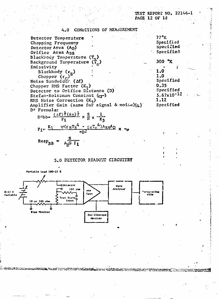
. TEST REPORY NO. 22146-l - PAGE 12 OF 18 .
4.0 CONULTIONS OF tfEAAIRE?fENT
Detector. Tcmpcrzkurc '. Chapping Frcqucncy . Detector Area (AD) ' Orifice Area ABB' Rlackboby Temperature (T ) Background Temperature (t-) - Emissivity I -
Blackbody (6,) I . Chopper (c 3 .
Noise Sandwig&. (Af) Chopper RXS Factor (X1) Detector to Orifice D~stante (3) Ste.fan-Boitzman Constant &) RNS Koise Correction (I$) Amplifier Gain (same for signal & noL?)(c)' D* Formula:
D;'bb= e@$.@d ; ' x -7% -- "3
5.0 DETECTOR READO'JT CIRCUfTXY
.
77*K SpecifPzd SpeciCteB
' SpCCiff@il
.
300 %
1.6 i ..-
2.0 Speci.fied . 0'.35 Specified 5.67x10-= . *-. 1.12 Specified
, . ! , 8
Blor Honlcor
.--

TEST REPORT NO. 22146-l PAGE 13 OF 18
6.0 HMDLING AND PRECAUTIOXS FOR HRC PRECISION L.R. DErECTOX
This precisfsn infrared detector was built in the laboratories of the HanPywell Radiation Center under the utmost care. This ,device was pro&ted using some of the most modern technology in existence. Howeve t, as with any precision piece of equipinent, there are toler- ance limitations.to which it C.An be subjected physicaily, thermally, and electrically.
6.1 Operating Temperature
The device is designed to operate at the approximate temperatures noted in Section 2.0 of this report.
6.2 Storage
This unit is designed to be stored at temperatures LIP to 185*F (8YCJ for short periods of time. Do not exceed this limit. Pro- longed exposure to high temperatures may prcduce a degradation of device performance.
6.3 Window and Housing
ParLs may cr.xk or break if subjected to hi h impact. Always transport device in the container in which H t was shipped.
6.4 DetLxtor Element Burnout --L 'The detector element is capable of dissipating only milliwatts of pouer. Do aot overbias. -- A. Caution: If lead from detector device should break contact
with the test circuit:
:: Turn off bias and amplifier power source. Discharge coupling capacitor b shorting test leads.
3. Reconnect detector elament to b ihs supply. 4. Turn bias power on again.
B. Uhen the detector is connected to any power source, there must be no voltage differential between the contacts until after circuit is complete.
C. Do not use any amplifier circuitry that will produce current . iZC2 detector or generate c-urrent surges.
D. The detector should be operated only in the ccoled condition. lf it i? pc-ssib1.e that the cooling unit may malfunction with- out ope::ator's kncwledge, the manufacturer suggests that a current/voltage limit.er be installed in the bias circuit to preverlt a runaway condition when the detector element warms.

.- -, . . . - *. _ . _ -. _ . - - _. _
TEST REPOR+ Pr‘O. 22146.? PAGE 1, OF 18
6.5 Protection from Meter Volts
~. Normally, the meters used to measure resistance utilize a 1.5 volt battery. The current generated by the battery is sufficient to
_ cause detector burnout. Therefore, if it is necessary to measure resistance, observe the following:
Use a Wheatstone bridge with an external battery to produce a current/voltage level compatible with the maaufacturer’s test results.
-. . . I . .
. .
L . .
i .
B. When the device is in an o erating circuit or syst.em, use a VTVM with selector switc K set to voltage. Read voltage drop across detector and compute resistance by Ohm’s Law. Re ‘cautious of power ground loops between VTVM and detector circuitry. Connect common ground first; then consect VTW to high side of detector. If VTVM is of a high impedance, it is advisable to use a series limiting resistance in VWM lead. Resistance values up to 1% of VTVM input impedance will cause no voltage reading errors.
6.6 Moisture
Before cooiing, remove ali traces of moisture in the dewar well. This will minimize therma 1 transfer problems and prevent dewar well breakage caused by t.he expansion of water when it freezes.
J I I ,
i 2..
. -*...-...---.-_ .._ * __

TEST REPrlT NO. 22146-l PAGE 15 OF 18
7.0 OPERATING INSTRUCTIONS FOR THE EK46 PREAMPLIFIER PACKAGE
The amplifier assembly'contains three low noise preamplifiers (Hone]~ell EK:!S) and bias circclits. The gz&qge has the capability of switchi.k:.a; each detector to a single charnel output. Design allows t!-.at only one detector can be biased at any one time. Detector bias limit resistors are located internally in the EY28 preamplifiers. Nomiaai bias limits are as ~011~s:
Channel1 - i mill iamperes Channel 2 - 8 mill iamperes Channel 3 - 8 milliweres.
1.) Eetector Bias Circuits
Detector Bias currents are set by the "Bias Control" and monitored by the bias current meter on the front panel. More accurate settings, are made using a DVM at the "Detector Test Point Terminals." The "I" position of the "I", "E", and "OFF" switch associated with the test jacks aliows the detector current to Le measured in terms of a voltage drop across a precision ,1X 100-n resistor in series with the dezector. The "E" position allows direct reading of the voltage drop across the detector. The "OFF" position removes the DVM from
the circuit.
2.) Detector Selector Switch This Esed to alternately switch Channels Dl, D2, and D3 to their proper preamplifier, the output of which is connected to the "Signal CA&put. ” The switch passes through a shorting position to insure that any extraneous charge at the preamplifier input is grounded out prior to connecting the detector.

. . .d - . .s . . . . , . , . - ._ ,_ - . - . :a . / .L . . . . , . .~ . . - = . - - . . ,_ . . . . _ d. . . . . . . . , , + . - _ - . . . . . . -.r l - - . -e_ . - . . . __ . -___ I . - _
T E S T R E P O R T N O . 2 2 1 4 6 - 1 P A G E 1 6 O F 1 8
3 .) ~ ~ A - m n l i fie r P o w e r
O n - O ff sw i tches fo r th e amp l i f i e r p o w e r supp ly .
4 .) M T R S h o r t
S w i t+ l th a t wi l l sLa r t o u t th e cu r ren t m e ter, if des i r ed . 4
S .i D e tecto r S h o r t
Th is is a p ro tect ive swi tch u s e d to p l a ce a shor t ac ross a n y d e tec to r a t the iT:put. It s h ou l d b e i n " sho r t ed " pos i t i on w h e n c o n n e c tin g o r d i sconnec t i ng d e tectors.
6 .) Test G a in In p u t 1 0 0 0 /t I,
A no rma l l y sho r t ed 1 1 1 - 1 % res is tor is w i r ed i n se r i es w i th th e d e tec to r re tu rn l eads . It is fe d b y a 1 C O O J L 1 % res is tor c o n n e c te d
I
I to J4. Th is p r ov i des a 1 0 0 0 /l s i gna l a tte n u a tio n a n d a l l ows a m e s n s o f i n jec t i ng a s i gna l i n th e mp l i f i e r i n p u t w i th its d e tec.tor i n th e c i rcui t a n d ca l i b ra t i ng th e g a i n o f e a c h amp l i f i e r w i thou t s ign i f icant ly c h a n g i n g th e i n p u t res is tance.
7 .) Z a p Inh ib i t o r Ci rcu i t
S i nce app l i ca t i on o f excess i ve p o w e r to th e d e tecto rs wi l l c a u se d e g r a d a tio n o r c o m p l e te b u r n o u t, e . p ro tect ive c i rcui t is p r o v i d ed th a t wi l l sho r t o u t th e d e tec to r if th e vo l t age ac ross th e d e tec to r r ises a b o v e a p rese t va lue . S h o u l d th i s occur , th e "B i a s P o w e r " swi tch must b e s h u t o ff a n d th e "B i a s C o n tro l " m u s t b e set to ze ro ;
th e shor t c a n th e n b e r e m o v e d by th e " A n t i -Zappe r " reset switch.
-.
.
' IZST REPORT N’o. 22146-1 PAGE 17 OF 13
NOTE : During shipment, the batteries were d iscdnnected. The back panel can be unscrewed; the outside of the hous ing can then be slibhtly puii .* forward and up to al low the batteries to be connected to the circuits. Batteries and wires are labeled.
.

TEST REPORT NO. EK46A). SCHEMATIC 'PAGE18 OF 18
22146. 1
,
. . .
.
.
.
