telequipment d61a osciloscope instruction & service manual
TRANSCRIPT
TELEQUIPMENF
DANGER
It is not possible to screen all high voltages, so care should be takennot to touch high voltage tags. Also where possible the instrumentshould be unplugged AND switched off during servicing. A BLEEDERPATH FOR THE EHT IS NOT PROVIDED~.so after switching offand before touching any internal parts, the EHT should be dischargedby temporarily shorting the appropriate points to chassis, (forinstance the CRT cathode pin and PDA connector where applicable).
FOR SERVICING AND SPARES ENQUIRIESSEE THE IN FORMATION AT START OF SECTION 5.
TELEQUIPMENT is a registered trade mark of TEKTRONIX U.K. LTD.
TEKTRONIX U K. LTD313 Chase RoadSouthgate,London N14 6JJENGLAND.
Telephone01-882 6100Telex: 262004Cables:TELEQUIPT LONDONN14
TEKTRONIX INC.,P.O Box 500Beaverton,Oregon (97005)U.S.A.
Telephone:(503) 644-0161Telex: 360485Cables:TEKTRONIX
DSCILLDSCDPE
TYPE D6IA~
INSTRUCTION MANUAL
Pc~S4bÇ~t(,9
YmLic~’vrn~x1 ~‘)
Q7Q-2019-00
~d~
I
Issue 6(711101)February 1977©Copyright (1975) byTektronix U.K. Ltd.
Printed in England by D & H NEWMAN LTD, 29 Harcourt Street, London Wi. 01 262 6356
— — — — — — — — — — — — — — — — — — —
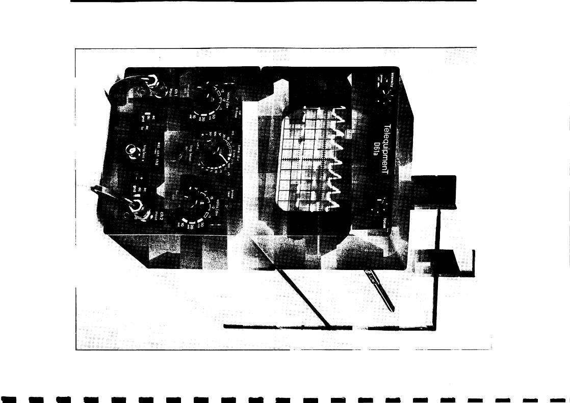
The D61A is a 10 MHz solid state dual trace oscilloscope using FET input circuitry for minimumdrift and fast stabilization time. A CAT with 8 cm x 10 cm face provides a bright and clear display.The dual trace vertical amplifiers provide the facility for each channel to be displayed separately,
alternately or chopped between channels. Channel 2 can be switched to become the horizontalamplifier to provide an X — Y display.
The design of this instrument is subject to continuous development and improvement,consequently this instrument may incorporate minor changes in detail from the informationcontained herein. These changes which usually affect the Component Lists and Circuit Diagrams aredescribed on Amendment Lists issued at regular intervals and are located in the pocket inside theback cover.
In addition to the standard instrument, variations known as Options are available and are
listed in Section 7 of this manual.
NOTICE TO OWNER
To obviate the risk of damage during transit and to facilitate packaging the owner is requested
NOT to send the following items unless they are suspect, should this instrument be returned toTEKTRONIX for servicing.
Manual
Probes
Plug Assemblies
CONTENTS
Page SECTION
1 SPECIFICATION 3 CIRCUIT DESCRIPTION
Cathode Ray Tube (CAT)CoolingHorizontal Deflection
External Horizontal amplifierSweep rates
Outputs Front PanelCalibratorProbe test
Power SupplyConsumption..Supply frequencySupply voltages
SizeTemperature limitsTrigger
Coupling
1/11/2
1/11/1
1/21/2
LevelSensitivitySource
Vertical AmplifierBandwidthDeflection factorsOperating modesX—Y
Weight
2 OPERATING INSTRUCTIONS
Additional facilities — Use ofAC—TVSlopeTrigger sourceTrig level
Basic applications
1/21/21/21/21/2
1/21/21/21/2
1/11/11/11/11/2
2/32/32/32/3
Attenuator and Vertical input amplifier .. 3/1C.R.T. Circuit and Power Supply .. .. 3/2Horizontal amplifier .. .. .. .. 3/2Vertical Output Amplifier .. .. .. 3/1Timebase, Unbianking and Bright line
auto circuit .. .. .. .. .. 3/1Trigger circuit .. .. .. .. .. 3/2
4 MAINTENANCE AND RE-CALIBRATION
Calibration Proced ureAstigmatism and GeometryHorizontal AmplifierInitial settingInternal calibratorSupply line voltagesTrigger and sweepVertical amplifier
IntroductionCalibratorGeneralTools and Equipment
MechanicalAccess to interior
4/24/24/14/34/14/34/2
4/14/14/1
4/14/14/14/1
C.R.T. removal ..
Re-fitting C.R.T.Replacing intensity or focus controls
5 COMPONENT LIST
Correction formula for fastrise time waveforms
Frequency measurementInstantaneous voltage measurement with
reference to a DC voltageInstantaneous voltage measurement with
reference to groundMonitor or display — Use as.Peak to Peak voltage measurementRise time measurementsVoltage measurement between two
points on a waveform ..
First time OperationSetting the controlsSwitch on
Operation of ControlsC.R.T.HorizontalVertical
Pre Operational check
2/32/32/4
2/4
2/22/2
2/12/12/12/1
2/52/4
Electrical components ..
Mechanical parts.. ..
..
..
..
..
..
..
5/25/8
2/4
2/4 6. CIRCUIT DIAGRAMSFigure
Power Supply and C.R.TPrinted Circuit Board PC 156 ..
..
..
..
..
57
Sweep Generator ..
Time/Div SwitchVolts/Div Switch )Trig Input and Horizontal AmplifierVolts/Div Switch and Vert Input amplifierCH1CH2‘Y’ Amplifier .. ..
Pre Set Controls diagram)Printed Circuit boards at end of chapter
4
6
3
1AlB2
7 OPTIONS
Option 1Option 4Option 6
SECTION Page
2/78
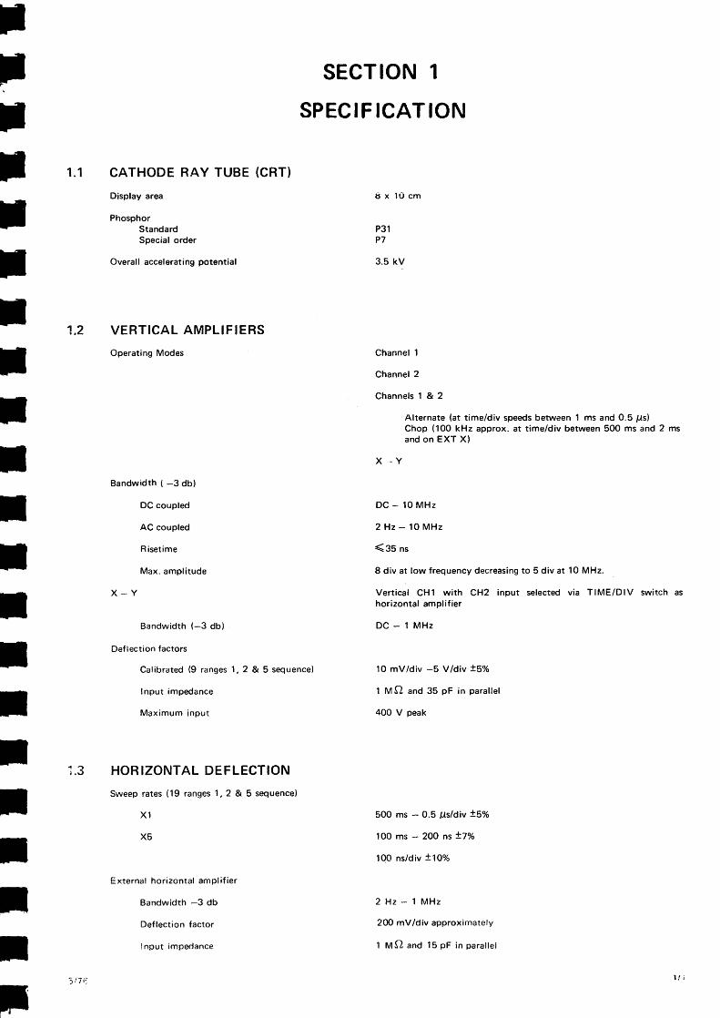
Display area
Phosphortandard
Special order
Overall accelerating potential
ERTICAL AMPI
Operating Modes
Bandwidth (—3 db)
DC coupled
AC coupled
Risetime
Max. amplitude
X—Y
Bandwidth (—3 db)
eflection factors
Calibrated (9 ranges 1, 2 & 5 sequenc
Input impedance
Maximum input
SPEC iF ICA1
x 10 cm
31
5 kV
Hz — 10 MHz
35 ns
(at time/div speeds b)0 kHz approx. at timXT X)
div at low frequency decreasing to 5 div at 10 MHz.
DC — 1 MHz
10 mV/div —5 V/div ±5%
1 M~and 35 pF in parallel
HORIZONTAL DI
Sweep rates (19 ranges
Xl
)0 ns/div ±10%
1.1
is and 0.5 /.Ls)en 500 ms and 2
is/div ±5%
Hz — 1 MHz
I1.4 TRIGGER I
Level Variable orVariable limited with auto free running in absence of trigger signal
Coupling AC orTV field for sweep ranges up to 100 ps/div andTV line from 50 ps/div to 0.5 ps/div
Source CH1, CH2 or external. All positive or negative
Sensitivity
Internal
40 Hz - 1 MHz 0.5 div minimum amplitude required becoming 1 div at 10 MHz
External
External, trig level only.40 Hz. 1 MHz 100 mV minimum amplitude required
1 MHz - 10 MHz 1 V minimum amplitude required a1.5 OUTPUTS FRONT PANEL
Calibrator peak to peak 500 mVsquarewave ±2%at supply frequency.
Probe test 2.5 V approximately rectangular pulse at sweep repetition rate and
sweep width.
1.6 POWER SUPPLY
Supply Voltages The instrument will operate at any selected one of the following voltages
107V ±10%117V ±10%214V ±10%234V ±10%
Supply frequency 48 - 440 Hz
Consumption 25 VA
1.7 SIZE IHeight 280 mm
Width 160 mm
Depth 420 mm
1.8 WEIGHT Bkgs
1.9 COOLING Convection
1.10 TEMPERATURE LIMITS, ambient
Operating 15 to +40°C
Non-operating — 25 to +70°C
II
1/2 8/77
I
SECTION 2OPERATING INSTRUCTIONS
2.1 PRE OPERATIONAL CHECK 2.2 OPERATION OF CONTROLS
2.1.1 GENERALAlthough this instrument is robust and is subjected tostringent checks before leaving our factory, it should bechecked externally for possible damage. In the case ofdamage contact the carriers and your local Tektronixfield office immediately.
Before switching the instrument on it is generallyrecommended that this section of the manual is read rightthrough and that some time be spent in becoming familiarwith the controls but experienced oscilloscope users mightfind the instructions in paragraph 2.4 rather laboriousso it is left to the individual user to decide what toomit reading.
The D61A relies on convection cooling and careshould be taken to see that external air circulation isnot restricted.
2.1.2 SUPPLY VOLTAGE ADJUSTMENTBefore operating the instrument it is necessary to adjustfor the available ac supply by means of the voltageselector plug, on the rear panel. Provision is made forselecting 107V, 117V, 214V and 234V. The plug shouldbe set to the nearest voltage to the available supply whichshould be within 10% of the tapping selected. The selectoris set by pulling out the plug and rotating until theselected voltage is opposite the indicator mark. The plugshould then be pushed back into the socket.
2.1.3 SUPPLY FUSEThe fuse holder is situated on the printed circuit boardinside the rear cover and if it is necessary to change thesupply tapping then the fuse should be checked forcorrect rating. For operation on 107V or 117V a 500mAfuse should be fitted and on 214V or 234V the fuseshould be 250mA. To gain access to the fuse holder itis necessary to remove the rear cover (see paragraph 4.2.1).
2.2.4 HORIZONTALTIME DIVISION
2.1.4 SUPPLY CABLE (OR POWER CORD)One of two types of supply cable will be fitted to theinstrument. For the American continent a lead with amoulded three pin plug will be supplied. For the rest ofthe world the three core lead has short tails left forconnecting to a plug top suitable for connection to thelocal supply system. The cores of this cable are colourcoded as follows.
LINE Brown
NEUTRAL Blue
EARTH Green/Yellow X5 When the X5 switch is pulled out
the sweep speeds are magnified bya factor of 5 and therefore thesweep range becomes 100 ms/divi-
For safety reasons it is important that the earth wire is sion to 100 ns/division.connected and if an extension lead is used it is essentialthat there is earth continuity. POSITION ~-* The X POSITION control uses the
BEFORE REMOVING THE REAR COVER DIS.CONNECT THE INSTRUMENT FROM THE SUPPLY
2.2.1 C.R.T.INTENSITY Varies the’ display intensity. An
instrument ON/OFF switch isfitted to this control.
FOCUS Controls the display definition.
TRACE ROTATION This control is fitted on therear of the instrument. It allowsthe trace to be aligned withthe horizontal graticule lines.
2.2.2 VERTICALVOLTS/DIVISION Provides attenuation of the input
signal in 9 calibrated steps. In theX — Y mode, CH1 provides thevertical input and CH2 the hori-zontal input.
POSITION ~ Moves the respective trace in theY or vertical axis. A channel ON/OFF switch is fitted to thiscontrol.
AC/DC/GND This selects the input coupling.In the AC position a capacitor isin series with the input, whilst inthe DC position the signal iscoupled directly to the attenuator.In the GND position the input isdisconnected and the amplifierinput is grounded. This allows aO V dc level to be established.
2.2.3 TRIG The slide switch is used to select(Pick off) channel 1 ,channel 2 or an external
source to provide a triggeringpulse (see 2.2.4 below).
Selects the sweep speed, therebeing 19 calibrated steps in therange 500 ms/division to 0.5 ps/division. Also EXT X or CH2(X — Y) MODE can be selected.On EXT X and sweep speedsbetween 500 ms/division and2 ms/division the display chopsbetween channels at approxi-mately 100 kHz/sec. On sweepsspeeds between 1 ms/division and0.5 ps/division the display alter-nates between channels.
3/77 2/1
same knob as tne speed magniT~er.When it is rotated is moves thetrace is an Xor horizontal axis.
Triggering is normally AC coupledbut when TV is selected triggeringis from a TV field at sweep speedsof 0.5 s/division to 0.1 ms/divisionand from a TV line at sweepspeed of 50 ps/division to 0.5 ps/division.
Enables the sweep to be triggeredeither externally or internally fromeither channel of vertical amplifier.
This switch allows triggering on apositive or negative slope of aninput waveform. On the TV posi-tion + refers to a positive goingpicture signal and — to a negativegoing picture signal.
The level control selects the volt-age level of the input waveform atwhich the sweep starts. With theknob pulled out the AUTOposi-tion is selected. In this position therange of level control is restrictedto a total of 2.5 divisions. In theabsence of an adequate trigger sig-nal the sweep generator free runsproviding a stable reference.trace.
These sockets connect the inputsignal to the respective verticalamplifiers.
The sockettriggering ortrigger ordependantswitch position.
Situated On the rear panel andconnected via an isolating capa-citor to the grid of the CRT. Apositive going signal is necessaryto intensify the trace with 10 ~Jamplitude providing a good con-trast. A negative going signal ofsimilar amplitude will blank thetrace.
A squarewave of 500 mV ampli-tude at supply frequency isprovided at this socket to allowfor the checking of the calibrationof the Vertical channels or fortriggering the sweep at supplyfrequency.
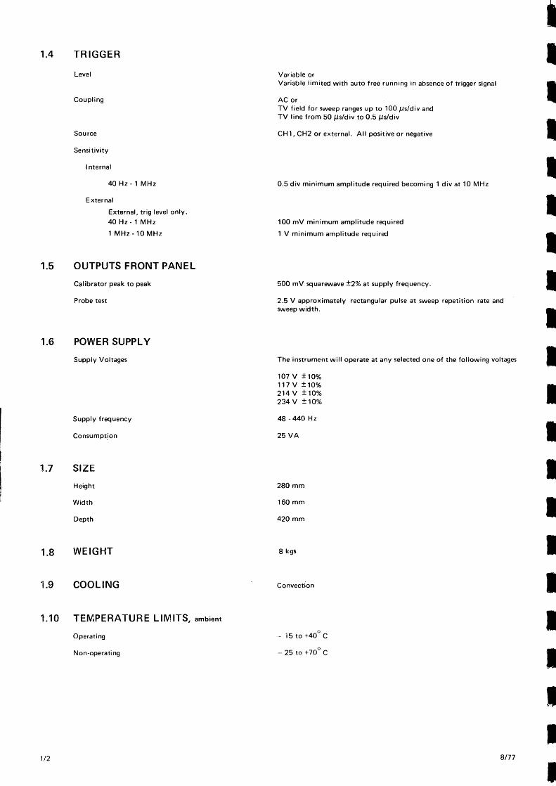
Provides a rectangular pulse attimebase frequency to facilitatethe setting up of probes. To set upthe probe compensation operateas follows:—1. Connect the probe to the in-
put socket of the channel withwhich it is to be used and setthe EXT-CH1-CH2 switch tothe other channel.
2. The TRIG LEVEL controlshould be turned fully anti-clockwise and pulled out tothe AUTOposition.
3. The TIME/DIVISION controlshould be set to 500 ps/divi-sion.
+— +
4. The appropriate VOLTS/DIV-SION control should be set to0.05 V/division.
5. The probetip should be appliedto the PROBE TEST socketand the probe trimmer adjustedso that the leading corner ofthe display is free from underor over shoot. The illustrationbelow shows three conditions:(a) over compensated;(b) correctly compensated;(c) under compensated.
Connect the CAL 0.5V socket (4mm) to input socket 1.For this operation a lead of 75~2Co-axial cable is requiredwith a BNC plug at one end and a 4 mm plug at theother. It should be possible to construct such a lead usinglocally available parts but in case of difficulty contactyour local TEKTRONIX field office.
I
AC/TV
EXT-CH1 -CH2
TRIG LEVEL
IIIII
2.3 INPUT AND OUTPUT SOCKETS
II
connects either aEXT X signal to thehorizontal circuits,
on the TIME/DIV
IUCH1
INPUTCH2
TRIG/EXT X
Z MOD
CAL
PROBE TEST& probe compensation
A
B
C
0.5 VOLT/DIV500pSEC/DIV
~ND This is connected to the chassis ofthe instrument.
2.4 FIRST TIME OPERATION2.4.1 SETTING THE CONTROLS
Set the front panel controls as follows:—
INTENSITY fully anti-clockwise - OFF
FOCUS Central
CH1 VOLTS/DIV 0.1 V
CH2 AC-DC-GND DC
CH1 Y POSITION Central
CH2Y POSITION Fully anti-clockwise (should clickoff)
EXT/CH1/CH2 CH1
TIME/DIV lOms
POSITION in and central
TRIG LEVEL in and central
AC-TV AC
IIII1II
2i~
III
2/76
I
2.4.2 SWITCH ON1. Switch on by turning the INTENSITY control
clockwise -
2. Allow a short while for a trace to appear.3. Centralize the trace using the X and Y (CH1)
POSITION controls.4. Adjust the INTENSITY control so that the trace is
at a suitable viewing intensity.5. Adjust the FOCUS control for the sharpest obtain-
able trace.6. Adjust the CH1 V POSITION control so that the
lower edge of the trace is level with one of the threelower graticule lines.
7. Observe that the overall waveform occupies 5 fullvertical divisions of the graticule.
8. Switch CH1 VOLTS/DIV switch to 0.2 V.9. Observe now that the trace will only occupy 2%
vertical division of the graticule.10. Disconnect the input from CH1 INPUT leaving
only a reference trace, which can be aligned withthe graticule lines by using the TRACE ROTATION~control, which is the lever sticking out of the topof the instrument, under the rear handle end piece.
11. Connect the input plug to CH2 INPUT.12. Set the EXT-CH1-CH2 switch to CH2.13. Switch on CH2 by rotating CH2 V POSITION
control clockwise until a click is heard. Furtherrotation will move the trace up the screen.
14. Set the lower edge of the trace to a suitable refer-ence line and observe that the trace occupies 5 fullvertical divisions.
15. Turn the CH1 POSITION control fully anti-clockwise to the OFF.position and note that CH2trace brightness increases. Leave CH1 off.
16. By now the user will be conversant with theoperation of the V or vertical controls so now theyshould turn to the sweep controls. By turning theTIME/DIV control anti-clockwise in steps as far asit will go, it should be noticed that the sweepspeed decreases. ~-. .c.~..,.4
17. Set the TIME/DIV knob to 1 ms and observe thenumber of cycles.
18. Set thé TIME/DIV knob tolOms and note thatmore cycles of the waveform should be seen.
19. Pull out the X5 control and observe that thedisplay should be double that in 17 above.
2.5 USE OF ADDITIONAL FACILITIES2.5.1 TRIGGER SOURCE
We have been using the control in the INT position but itis possible to trigger from an external signal by pluggingthe signal into the TRIG/EXT X socket. The EXT-CH1-CH2 switch should be set to EXT.
2.5.2 SLOPE (+ or —)
The + — switch allows triggering from a positive (+) goingor negative (—) going portion of the trigger signal. This isimportant when it is only required to observe a portion of; waveform but where several cycles of a waveform aredisplayed the setting is often unimportant.
2.5.3 AC-TVForthe inspection or measurement of most waveforms theAC-TV control is used in the AC position. For theinspection of TV field or TV line waveforms the switchshould be set to TV, and the + — switch to + for positivegoing picture signals or — for negative going picturesignals. For TV field waveforms sweep ranges of 0.5 sec/div to 0.1 ms/div should be used. For TV line waveformssweep ranges of 50 ps/div to 0.5 ps/div are required. Inthe TV position the Level control is inoperative but theAuto position still gives a trace in the absence of a TVsignal of sufficient amplitude to trigger the oscilloscope.
2.5.4 TRIG LEVELThere are two modes of LEVEL control operation. Inthe normal (control IN) position the triggering point canbe varied over the whole of the waveform to a maximumof 8 divisions for a symmetrical waveform.
In the AUTO position (control OUT) level control isrestricted to approximately 2% divisions, and the timebase
free runs in the absence of a trigger signal.
2.6 BASIC APPLICATIONSThe following are typical applications of oscilloscope typeD61A. Only outline procedures are given to allow theuser to adapt the method to individual requirements.Familiarity with the controls of the instrument a~out-lined in 2.2, 2.3 and 2.4 should allow these basic tech-niques to be applied to a wide variety of uses.
2.6.1 USE AS A MONITOR OR DISPLAYOne of the most frequent uses of an oscilloscope is as amonitor or display. By correct adjustment of the X and Ycontrols it is possible to displaymany cycles or a fractionof one cycle of a repetitive waveform. Generally it isdesirable to limit the display to the centre 6 divisionsvertically and in the case of a repetitive waveform todisplay 1 to 8 cycles within the centre 8 divisions hori-zontally. It is possible to use the D61A instrument in thisway to inspect a waveform for slope, over or undershootand ringing. Where it is required to compare two wave-forms, such as the waveforms entering and leaving adevice, it is possible to feed the two waveforms tothe two channels and display them either vertically oneabove the other, or superimposed.
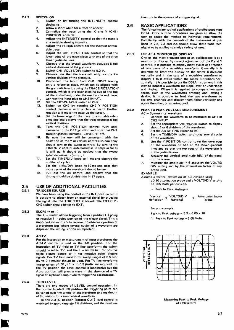
2.6.2 PEAK TO PEAK VOLTAGE MEASUREMENTAC — Symmetrical waveform1. Connect the waveform to be measured to CH1 or
CH2 INPUT.2. Set the appropriate VOLTS/DIV switch to display
about 5 or 6 divisions of the waveform.3. Set the AC-DC-GND switch to AC.4. Set the TIME/DIV switch to display several cycles
of the waveform.5. Use the Y POSITION control to set the lower edge
of the waveform on one of the lower graticulelines and so that the top edge of the waveform isin the graticule area.
6. Measure~the vertical amplitude (div) of the signalon the screen.
7. Multiply the amplitude in 6 above by the VOLTS/DIV setting and by the attenuation factor of anyprobe used.
EXAMPLEAssume a vertical deflection of 5.3 division using
a X10 attenuation probe and a VOLTS/DIV settingof 0.05 Volts per division.
Peak to Peak Voltage =
Vertical X VOLTS/DIV
deflection (Setting)
for our example
X Attenuator factor(probe)
Peak to Peak voltage 5.3 x 0.05 x 10.‘. Peak to Peak voltage 2.65 Volts.
Measuring Peak to Peak Voltageof a Waveform
2/76 2/3
2.6.3 VOLTAGE MEASUREMENT BETWEEN TWO POINTSON A WAVEFORMProceed as in 2.6.2 above substituting the two measure-ment points for the peaks and setting the lower point onone of the lower graticule lines.
2.6.4 INSTANTANEOUS VOLTAGE MEASUREMENT WITHREFERENCE TO GROUNDTo make a measurement of the DC level at a specifiedpoint or. a waveform use the following procedure.1 - Set the AC/DC/GND switch of the selected channel
to DC.2. Set the EXT/CH1/CH2 switch to .the channel
selected.3. Pull the TRIG LEVEL control out to the AUTO
position-4. C.nnect the waveform to be measured to the
INPUT of the selected channel.5. If the waveform is repetitive use the TIME/DIV
and X POSITION (+—~). controls to displayat leastone cycle.
6. Switch the AC/DC/GND switch of the channel inuse to GND.
7. Set the trace to the lowest graticule line or othersuitable reference line, using the V POSITIONcontrol, if the point to be measured is positive.Set to highest or other suitable graticule line ifthe point to be measured is negative. AFTERTHIS DO NOT ADJUST THE Y POSITIONCONTROL.
8. Set AC/DCIGND switch to DC.9. Measure the distance in divisions from the refer-
ence line to the point to be measured.10. Establish the polarity of the measured voltage.
If the measurement point is above the referenceline the voltage is positive. If the measurementpoint is under the reference line it is negative.
11. Multiply the estimate in (9) above by the VOLTS/DIV switch setting and any probe attenuationfactor.
EXAMPLEAssume that the veritcal distance measured is +23divisions with a VOLTS/DIV setting of 200 mVand the probe attenuation factor is Xl
Instantaneous —
voltage —
For the values given
Instantaneous voltage = 2.7 x 1 x 0.2 x 1
.. InstantaneousVoltage = 0.54 Volts
2.6.5 INSTANTANEOUS VOLTAGE MEASUREMENT WITHREFERENCE TO A DC VOLTAGEProceed as in 2.6.4 but in step (6) set the switch to DCand feed in the reference voltage to the input. step 8 willbe to remove the reference voltage.
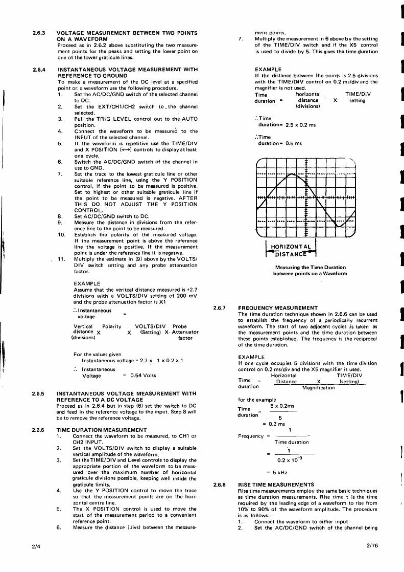
2.6.6 TIME DURATION MEASUREMENT1. Connect the waveform to be measured, to CH1 or
CH2 INPUT.2. Set the VOLTS/DIV switch to display a suitable
vertical amplitude of the waveform.3. Set the TIME/DIV and Level controls to display the
appropriate portion of the waveform to be meas-ured over the maximum number of horizontalgraticule divisions possible, keeping well inside thegraticule limits.
4. Use the V POSITION control to move the traceso that the measurement points are on the hori-zontal centre line.
5. The X POSITION control is used to move thestart of the measurement period to a convenientreference point.
6. Measure the distance (Jivs) between the measure-
Vertical Polaritydistance X
(divisions)
VOLTS/DIV ProbeX (Setting) X Attenuator
factor
ment points.7. Multiply the measurement in 6 above by the setting
of the TIME/DIV switch and if the X5 controlis used to divide by 5. This gives the time duration
EXAMPLEIf the distance between the points is 2.5 divisionswith the TIME/D.IV control on 0.2 ms/div and themagnifier is not used.Time horizontal TIME/DIVduration = distance X setting
(divisions)
.~.Timeduration= 2.5 x 0.2 ms
..Timeduration= 0~5ms
Measuring the Time Durationbetween points on a Waveform
2.6.7 FREQUENCY MEASUREMENTThe time duration technique shown in 2.6.6 can be usedto establish the frequency of a periodically recurrentwaveform. The start of two adjacent cycles .is taken asthe measurement points and the time duration betweenthese points established. The frequency is the reciprocalof the time duration.
EXAMPLEIf one cycle occupies 5 divisions with the time divisioncontrol on 0.2 ms/div and the X5 magnifier is used.
Horizontal TIME/DIVTime = Distance X (setting)duration Magnification
for the example5x0.2ms
Time =
dura~ion
Frequency = ____________Timeduration
= 0.2x103
= 5 kHz
2.6.8 RISE TIME MEASUREMENTSRise time measurements employ the same basic techniquesas time duration measurements. Rise time t is the timerequired by the leading edge of a waveform to rise from10% to 90% of the waveform amplitude. The procedureis as follows:—1. Connect the waveform to either input2. Set the AC/DC/GND switch of the channel being
5= 0.2 ms
II
II1IIIIIIIII
2/4 2/76
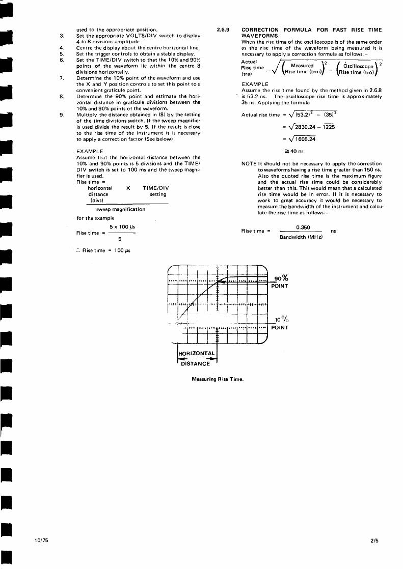
used to the appropriate position.3. Set the appropriate VOLTS/DIV switch to display
4 to 8 divisions amplitude4. Centre the display about the centre horizontal line.5. Set the trigger controls to obtain a stable display.6. Set the TIME/DIV switch so that the 10% and 90%
points of the waveform lie within the centre 8divisions horizontally.
7. Determine the 10% point of the waveform and usethe X and V position controls to set this point to aconvenient graticule point.
8. Determine the 90% point and estimate the hori-zontal distance in graticule divisions between the10% and 90% points of the waveform.
9. Multiply the distance obtained in (8) by the settingof the time divisions switch. if the sweep magnifieris used divide the result by 5. If the result is closeto the rise time of the instrument it is necessaryto apply a correction factor (See below).
EXAMPLEAssume that the horizontal distance between the10% and 90% points is 5 divisions and the TIM E/DIV switch is set to 100 ms and the sweep magni-fier is used.Rise time =
horizontal X TIME/DIVdistance setting(divs)
sweep magnification
for the example
5 x lOOpsRise time =
5
Rise time = loops
2.6.9 CORRECTION FORMULA FOR FAST RISE TIMEWAVEFORMSWhen the rise time of the oscilloscope is of the same orderas the rise time of the waveform being measured it isnecessary to apply a correction formula as follows:—
Actual Ii ‘2Rise time ~ ( Measured ) — ( OscilloscoPe) 2
(tra) Rise time (trm) ~Risetime (tro)
EXAMPLEAssume the rise time found by the method given in 2.6.8is 53.2 ns. The oscilloscope rise time is approximately35 ns. Applying the formula
Actual rise time = \/‘~ii~—(35)2
= ~/2830.24 — 1225
= ~[1605.24
~40 ns
NOTE It should not be necessary to apply the correctionto waveforms having a rise time greater than 150 ns.Also the quoted rise time is the maximum figureand the actual rise time could be considerablybetter than this. This would mean that a calculatedrise time would be in error. If it is necessary towork to great accuracy it would be necessary tomeasure the bandvvidth of the instrument and calcu-late the rise time as follows:—
0.350Rise time = fls
Bandwidth (MHz)
Measuring Rise Time.
10/75 2/5
CIRCUIT
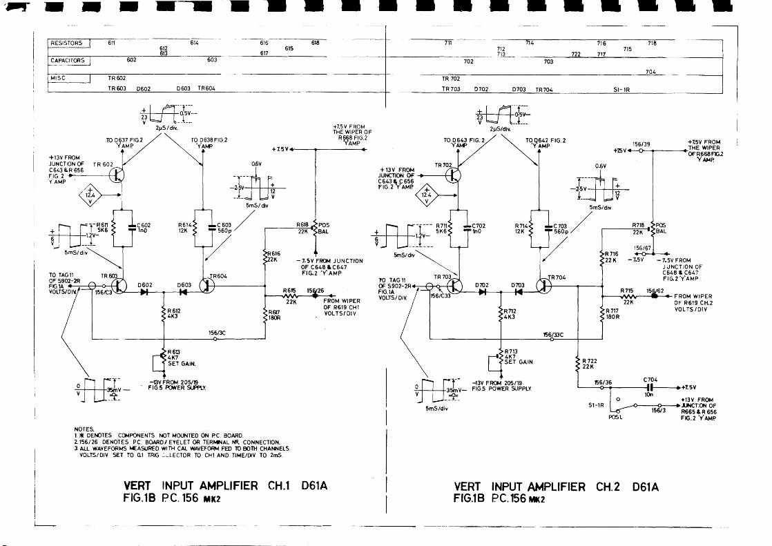
ATTENUATORAND VERTICAL INPUTAMPLIFIER Figures 1A& lB.
CH1 and CH2 are identical and the following descriptioncovers both channels.
The input to the attenuator is connected via C901 tothe input socket SK9O1 on AC, directly to the inputsocket on DC or to ground on GND. The capacity com-pensated attenuator is switched by S902 wafer 1 in stepsof 100, 10 and 1 and the output is fed to the gate ofTR6O1 via C601 and R602 which, together with 0601,protect the input against overloads up to ±400V.TR6O1 is a F.E.T. source follower whose output DC levelis adjusted to zero by R604 and R608. The output is thenattenuated in steps of 5, 2 and 1 selected by S902 wafer2 F and fed to the base of TR6O3 which together withTR604 forms a longtailed pair. The diodes 0602 and0603 in the emitters increase the signal handling capacity
~ut affecting the change inly proportional to current ane. This compensates for the~rselyproportional to supplyI vertical sensitivity remains ie. Vertical shift is fed to thf the channel is set up by RIstage emitter current. The~ ~nd TRFfl4 n~c
SECTION 3
ESCR IPT ION
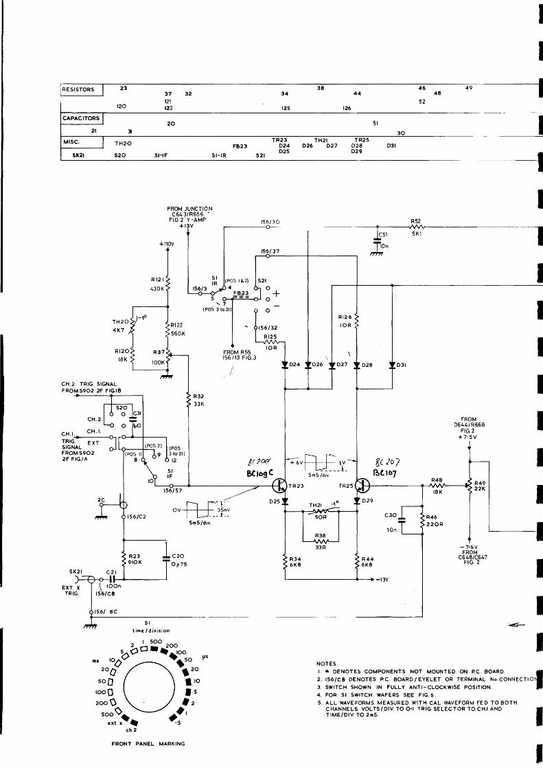
3.2 TRIGGER CIRCUIT Figures3&4
This consists of a Iongtailed pair TR23 and TR25 similarto the Vertical Amplifier input stage but with temperaturecompensation in its emitter circuit. On the CH2 positionthe input is connected to CH2 and EXT..X position viaC20, C21 and R23 to the TRIG/EXT X socket. On allother positions of the Time/Div switch the input isconnected to S20 which selects either the EXT TRIGsocket, CH1 or CH2 signal. The output from the appro-priate collector, selected either by the Polarity switch 821or the Time/Div switch Si, is connected via diode 027 orD31 to the emitter of common base stage TR26. Thecollector of TR26 is connected via D54, D33 and D34 tothe input of the Horizontal Amplifier on CH2 and EXT Xpositions of the Time/Div switch Si. On other positions ofthe Time/Div switch the collector of TR26 is AC coupledvia 032 to the base of TR21, a shunt feedback stage.
On the AC position of S22 the output of TR21 is con-nected via diodes D58 and 059, which limit the voltageswing, to the input of the Schmitt trigger circuit TR22and TR24. The Level control R2i allows the mean DClevel of the output of TR21 to be varied so that any por-tion of the trigger signal can be set at the triggering level
.g .1.._. C.L..:.. tAIL..... ,L.. I .....,..I .~..._I .... •1..,.. A.....
haretiv by
~J.
ducts and discharges the timing capacitor until D45conducts and reduces the current in TR34 to the valuerequired by the timing resistor. At this point the flybackstops. During the flyback the hold-off capacitor dischargesthrough Rii4 until D48 conducts. At this point theaction is complete and the timebase can be triggered bythe next triggering pulse.
3.3.2 1f the Trig level control is in the Auto position and notrigger pulses are present, TR34 and D49 conduct andreduce the potential at the anode of 048. This allows thehold-off capacitor to discharge further and re-trigger thebistable. The timebase then free-runs. If trigger pulses arepresent at the anode of 043 the positive pulses triggerthe monostable TR32 and TR35. When triggered at fre-quencies above about 10 Hz the average collector currentof TR35 is low and 049 is cut off returning the timebaseto the normal triggered condition.
3.3.3 The collector current of TR29 which is cut off during thesweep is fed to the input of TR28. The collector of TR28goes negative at the beginning of the sweep until diodeD38 conducts and clamps the collector potential at about3 V. thus unblanking the sweep. When TR29 conducts atthe end of the sweep TR28 collector goes positive blankingthe trace. On chop positions of the sweep negative edgesfrom the chop circuit are fed to the base of TR28 to blankthe trace during the transitions.
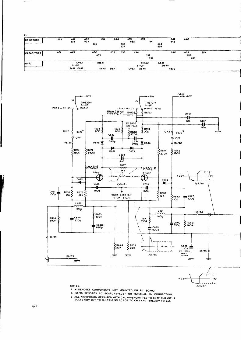
3.4 HORIZONTAL AMPLIFIER Figure 3
This consists of a shunt feedback stage TR31 withswitched feedback resistors to give X5 expansion. Thesweep and horizontal shift currents are mixed at the inputof the shunt feedback stage and the output is fed to aIongtailed pair, TR33 and TR37, which feeds the hori-zontal deflection plates of the CRT. 044 clamps thecollector of TR33 and prevents it from bottoming.
On the EXT X and CH2 positions of the Time/Divswitch the input of TR31 is switched to the collector ofTR26 via 033, 034 and D54 and the X5 feedback resistoris shorted Out by diodes 033, 034, D35 and D37. Thetrace is then deflected horizontally via the EXT X socketor from Channel 2. On these positions the gate of TR36
is connected to the cathode of D47 which clamps theoutput of the timebase at about +1 V and turns off TR29thus unbianking the trace.
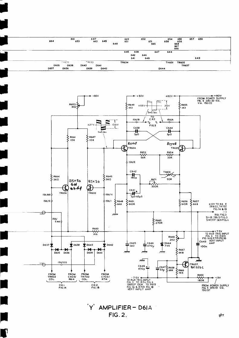
3.5 CRT CIRCUIT AND POWER SUPPLY
The supply voltage is fed via the power ON/OFF switchS401, the fuse FS4O1 and the voltage selector SK4O1 tothe appropriate primary tapping on T40i.
3.5.1 The —13 V line is obtained from a full wave rectifiercircuit consisting of D405, 0406, C402 and R4O3.
3.5.2 The +117 V line is obtained from a bridge rectifier D401,D4O2, D403 and 0404 with reservoir capacitor C403 andsmoothed by R406 and C4OS to provide the +110 V lineand by R407 and C406 to provide the +80 V line.
3.5.3 The —1050 V line is obtained from a halfwave rectifiercircuit consisting of 0407, 0409, C4l 1 and C412.
3.5.4 The +2500 V line is obtained from a voltage doublercircuit consisting of 0408, D409, C40i and C404.
3.5.5 The calibrator circuit provides a 0.5 V squarewave atsupply frequency. It is produced by a diode switchingcircuit in which a current derived from the stabilized—7.5 V line is passed through 0413 and R4O8 duringnegative half cycles of the AC voltage from the 13 Vtransformer winding. On positive half cycles 0413 is cutoff and the current passes through 0412 and R402. Theoutput voltage is set by R405. The temperature coefficientof the diode 0413 is compensated for by the negativecoefficient of the output resistor R408 giving an outputvoltage which is nominally independent of temperature.
3.5.6 The grid voltage of the CRT is derived from a zener diodeconnected between the CRT cathode and the —1050 Vsupply. The voltage is varied by the intensity controlR301. The intensity of the trace may be varied by signalsfed via the Z Mod socket SK3O1 and C3O1 to the grid ofthe CRT.
I
Figure 5
IIIIIIIIIIIIIIII
3/2
III
10/75
I
SECTION 4
MAINTENANCE AND RE-CALIBRATION
Care must be taken not to touch high voltage tags. The instrument MUST BE UNPLUGGED when removing the case, removing or repla~ingthe tube, or other components and where possible during other servicing.
4.1 INTRODUCTION
4.1.1 GENERALThe solid state design of the instrument makes frequentadjustment of the internal preset components unnecessary.The appropriate part of the re-calibration procedureshould be carried out, whenever the instrument fails tomeet its specification, or whenever a defective componentis replaced. Section 3 should be helpful in deciding whichpart of the circuit requires adjustment.
4.1.2 CALIBRATORThe internal 0.5 V calibration signal allows the accuracyof the vertical amplifier system to be checked. Thecalibration signal which is at supply frequency can alsobe used to check the sweep speed to the accuracy of thesupply frequency.
4.1.3 TOOLS AND EQUIPMENTTo carry out the whole calibration procedure, thefollowing tools and equipment are required:—Low-capacitance trimming tool (for preset capacitors).Small screwdriver (for preset potentiometers).Amplitude Calibrator, providing 1 kHz squarewave, ampli-tude 50 mV, amplitude accuracy within 0.25%.Time-mark Generator, providing markers of 1 ms, 1 psand preferably, 0.5 ps. Accuracy within 0.1%.Squarewave Generator, providing outputs of 1 kHz and10 kHz, 50 mV to 50 V.Squarewave Generator, providing outputs of 10 kHz,100 kHz and 1 MHzwith rise-time less than 10 ns.Coaxial cable and terminating resistor for the above.Monitor Oscilloscope, complete with Xi0 passive probe,and having a sweep output socket.Passive Probe, X10 attenuation, suitable for input capaci-ties of 25 to 35 pF.Test Meter, 20,000 n/volt or higher, accuracy within 2%2.5 V DC to 2500 V DC.Composite TV video signal source.Sinewave Generator, 1 kHz, 10 kHz and 50 kHz.Co-axial leads allowing the same signal to be connectedto Channel 1, Channel 2 and the EXT socket.
4.2 MECHANICAL4.2.1 ACCESS TO INTERIOR
NOTE: UNPLUG INSTRUMENT FROM SUPPLYBEFORE REMOVING COVERS
The cabinet covers are removed as follows:—1. The back cover is removed by undoing and
removing the three fixing screws arid pulling thecover off.
2. The lower side panels can then be slid backwardsout of position.To re-fit the covers it is necessary to slide the lowercovers into position taking care that the slot on thelower edge engages with the raised portion of thelower panel bezel, and that the lug at the top isengaged. The rear cover should be slid into positionand the three screws inserted.
4.2.2 CRT REMOVAL1. Disconnect the instrument from the ac supply.2. Remove the covers as shown in 4.2.1 above.3. Short point k on the Printed Circuit board to chassis
via a 1 M~Zresistor and keep the short in place for
about 1 minute to discharge any residual highvoltage.
4. Remove the INTENSITY and FOCUSknobs.5. Remove the felt washers and the panel bearing
the name TELEQUIPMENT.6. Remove the 4 screws fixing the plastic bezel
surrounding the tube face and pull off the bezeland graticule.
7. Slide off the black section of the upper case bymoving forward.
8. Spring down the ends of the springy copper stripabove the tube and slide the strip out.
9. Pull off the tube base (at the rear of the tube)using the loop provided.
10. Loosen the screws holding the clamps which fix therear tube screen to the plastic moulding and slidethese clamps off.
11. Slide the tube gently forward easing the mumetalpast the lower support and chassis edge until thePDAcap is clear of the chassis.
12. Remove the PDA cap by pulling out and then slidethe tube right out of the instrument.
4.2.3 RE-FITTING CRTThe procedure for re-fitting is the reverse of 4.2.2 above.Care must be taken in easing the front of the mumetalscreen past the chassis edge, and in keeping the PDA capclear of the chassis front.
4.2.4 REPLACING INTENSITY OR FOCUS CONTROLSIf it is required to replace either of these controls it isnecessary to remove the C.R.T. as above to allow enoughroom to get to the extension spindles and fixing nuts.
4.3 CALIBRATION PROCEDURE
4.3.1 INITIAL SETTING1. Remove side covers, reference Para 4.2.1. Connect
to a suitable A.C. power source and switch theinstrument on.
2. Set the front panel controls as follows:—AC-DC-GND) GNDrVOLTS/DIV )CH1 & 0.01POSITION )CH2 Mid-positionTIME/DIV ) 1 msHorizontal POSITION Mid-position, push inTRIG LEVEL Mid-position, out (AUTO)+
EXT-CH1-CH2 EXTAC-TV ACFOCUSINTENSITY)
Adjust for well definedlovi brilliance trace
4.3.2 SUPPLY LINE VOLTAGES (R668)D.C. supply line voltages should normally lie within theprescribed limits when A.C. power source voltage coin-cides with the setting of the line voltage selector on therear of the instrument.
The —7.5 V line is adjustable by means of R668. Itshould normally only require re-setting when TR637 hasbeen replaced. If the movement of the trace is greaterthan 1 div when the mains voltage is adjusted to±10% ofnominal, use the following procedure:—
3/77 4/1
1. Set the Test Meter to a range suitable for measuring10V d.c.
2. Connect the negative test lead to test point 67 andthe positive test lead to chassis.
3. Set CH1 & CH2 AC-DC-GND to GND.4. Adjust R668 for a meter reading of 7.5 V approx-
imately.5. Re-check the trace movement for ±10% variation.6. If the specification cannot be met, raise or lower
the voltage setting which must remain within thelimits of 7 V to 7.7 V.
7. If P668 is altered, the Vertical Amplifier Balanceprocedures in 4.3.4 must be re-checked.
Supply Line Test Point Limits
— 7,5V~
CH1 POSITION potentiometerviolet-blue wire
—7.3V to —7.7V
+ 7.5V CH1 POSITION potentiometerorange-white wire
+7.1Vto +7.9V
— 13V Horizontal POSITION poten-tiometer mauve-white wire
—12.4V to —13.6V
+13V Test Point3 +ll.9Vto+12.1V
+ 80V Test Point 22 +75V to +85V
+110V TestPoint29 +l07Vto+ll7V
—1050V Test Point 156/7 —1060V to —i 160\
+2500V Test Point 156/K +2400V to +2500V
4.3.3 ASTIGMATISM AND GEOMETRY (R305 and R307)1. Set TIME/DIV to 100 ps and display a 10 kHz
sinewave signal on one channel only at 6 divisionsvertical amplitude.
2. Adjust FOCUS and R305 (Astigmatism) for bestdefinition of display. Leave 10 kHz signal connec-ted.
3. SetTIME/DIV tol ms.4. Select AUTO and ensure that no signal is con-
nected to EXT.5. Set EXT-CH1-CH2 switch to EXT so tnat display
becomes an unsynchronised raster.6. Adjust R307 so that the raster becomes as nearly
as possible rectangular.7. Disconnect 10 kHz signal.
4.3.4 VERTICAL AMPLIFIER
4.3.4.1 CHANNEL 1 VOLTS/DIV BALANCE (R604 and R608)1. Check that Channel 1 input switch is set to GND
and VOLTS/DIV to 0.01.2. Turn Channel 1 on, Channel 2 off.& Connect test meter between test point C3 and
chassis.t~4. Adjust P604 for zero reading. It should normally
be necessary to adjust R604 only when TR6O1 hasbeen replaced. After adjustment of R604, P613must be checked and re-adjusted If necessary. Seepara 4.3.4.5. Disconnect test meter.
~. 5. Switch Channel 1 VOLTS/DIV between 0.01, 0.02and 0.05 positions. Adjust R608 to eliminate verti-cal movement of the trace.
4.3.4.2 CHANNEL 1 POSITION BALANCE (R618)1. Connect test meter between Channel 1 POSITION
potentiometer moving contact (red-blue wire) andchassis.
2. Adjust POSITION for zero reading.3. Adjust P618 to bring the trace to the centre of the
screen.4. Disconnect test meter.
4.3.4.3 CHANNEL 2 VOLTS/DIV BALANCE (R704 and R708)1. Check that Channel 2 input switch is set to GND
and VOLTS/DIV to 0.01.
2. Turn Channel 2 on and Channel 1 off.3. Connect test meter between test point C33 and the
chassis..~ 4. Adjust R704 for zero reading.
It should normally be necessary to adjust P704only when TR7O1 has been replaced. After adjust-ment of R704, R713 must be checked and re-adjusted if necessary. See para 4.3.4.6.
~ 5. Disconnect test meter.~f 6. Switch Channel 2 VOLTS/DIV between 0.01,0.02
and 0.05 positions. Adjust R708 to eliminatevertical movement of the trace.
4.3.4.4. CHANNEL 2 POSITION BALANCE (R718)- Connect test meter between Channel 2 POSITION
potentiometer moving contact (red-blue wire) andchassis.
2. Adjust POSITION for zero meter reading.3. Adjust R7l8 to bring the trace to the center of the
screen.4. Disconnect test meter.
4.3.4.5 CHANNEL 1 GAIN (R613)1. Set Channel 1 VOLTS/DIV to 0.01 and Amplitude
Calibrator output to 50 mV.2. Display Amplitude Calibrator output on Channel 1.3. Adjust the amplitude of the display to exactly 5
divisions with P613.4. Disconnect Amplitude Calibrator.
4.3.4.6 CHANNEL 2 GAIN (R713)1. Set Channel 2 VOLTS/DIV to 0.01 and Amplitude
Calibrator output to 50 mV.2. Display Amplitude Calibrator output on Channel 2.3. Adjust the amplitude of the display to exactly 5
divisions with R7 13.4. Disconnect,AmpI itude Calibrator.
4.3.4.7 PULSE RESPONSE (C641, R671 and R653)1. Set both VOLTS/DIV to 0.01.2. Display a 1 MHz squarewave signal simultaneously
on both channels. (Ensure that the co-axial cableconnecting the signal to the instrument is correctlyterminated).
3. Adjust C641 and R67l to optimise squarewaveresponse on both channels. If the response of thechannels is not exactly the same, adjust for bestcompromise.
4. Adjust P653 to minimize the change in squarewaveresponse occurring when either POSITION controlis adjusted.
5. Disconnect squarewave signal.
4.3.4.8 ATTENUATORS (C902, C903, C904 and C905)Channel 1 and Channel 2 attenuators and input selectorcircuits are electrically identical. Corresponding compo-nents in these parts of the two channels carry the samecomponent references.
1. Set Channel 1 input switch to D.C.2. Display a 10 kHz squarewave of 0.5 V amplitude
on Channel 1, using the 0.1 VOLTS/DIV positionof the attenuator.
3. Adjust C905 for the best response (square cornerwithout overshoot or undershoot.
4. Set Channel 1 attenuator to 1 VOLTS/DIV andincrease the amplitude of the squarewave to 5V.
5. Adjust C904 for the best response.6. Disconnect squarewave signal.7. Connect a X10 passive probe to the input of
Channel 1.8. Set the Channel 1 VOLTS/DIV to 001.9. Display a 1 kHz squarewave of 0.5 V amplitude
via the probe.10. Adjust the probe compensation for the best
squarewave response.ii. Set VOLTS/DIV to 0.1 and increase ~heamplitude
of the squarewave to 5 V.12. Without altering the probe compensation, adjust
C903 for the best squarewave response.13. Set VOLTS/DIV to 1 and increase the amplitude
of the squarewave to 50 V.14. Adjust C902 for the best squarewave response.
4/2 3/77
15. Disconnect signal and probe.16. Repeat Ops 1 to 15 for Channel 2.
6. Discdhnect Calibrator.
4.3.5.3.
4.3.5 HORIZONTAL AMPLIFIER
4.3.5.1 OUTPUT STAGE BALANCE (R108 and R113)1. With TIME/DIV set to 2 ms display a 1 kHz signal
(sinewave or squarewave) on Channel 1.2. Adjust the horizontal POSITION control to the
point where the Iefthand end of the trace does notmove when the X5 switch is operated.
3. Without re-adjusting the-POSITION control, bringthe Iefthand end of the trace to the centre verticalgraticule line by adjustment of Al 13.
4. Position the trace centrally on the screen with thehorizontal POSITION control.
5. Adjust R108 for the best horizontal linearity atthe right and lefthand extremities of the CATscreen.
4.3.5.2 PRE-AMPLIFIER BALANCE (R37, R49 and R80)1. Set TIME/DIV to2 ms.2. Short tag C2 or the top lead of C20 to ground.3. Set EXT-CH1-CH2 switch to EXT.4. Connect test meter between test point (H—) and
Chassis (+).5. Adjust R49 so that the test meter reading is
independent of the position of the ±switch.6. Disconnect the test meter.7. SetTIME/DIVto1 ms.8. Adjust the lefthand end of the trace to the left-
hand edge of the -graticule by means of thePOSITION control.
9. Turn TIME/DIV to CH2 and bring the spot to thecentre vertical graticule line by adjusting R80.
10. Set TIME/DIV to EXT X.11. Bring the spot to the central graticule line by
adjusting A37.
4.3.5.3 CHANNEL 2 HORIZONTAL GAIN CR104)1. Set TIME/DIV to CH2.2. Set the output of the Amplitude Calibrator to
50 mV and connect to the input of Channel 2.3. Set Channel 1 input switch to GND and channel 2
input switch to A.C.4. Set Chennal 2 VOLTS/DIV to 0.01.5. Set horizontal deflection to exactly 5 division with
R104.
10. Set TIME/DIV to 100 ~1s.11. Turn R3l clockwise adjusting the LEVEL control
if necessary to maintain triggering until a positionis reached at which triggering can not be obtainedor, the pot is fully clockwise. Notesetting of R3l.
12. Adjust R31 to halfway between the two positionspreviously noted.
13. Remove the 10 kHz input signal.14. Feed a 1 div amplitude to 10 MHz sinewave to
CH1 and check that a locked trace can be obtainedby adjustment of the LEVEL control on both +veand -ve. If not turn A31 anticlockwise sufficientto obtain a locked trace but not as far as in 7 above.
15. Repeat 14 on CH2 both +ve and —ve.
4.3.6.2 SWEEP STABILITY (R74)1. Remove CAL signal.2. Apply a 1 kHz signal.3. Set TIME/DIV to 1 ms.4. Bring the RH end of the trace on to the screen
using the X POSITION control.5. Adjust R74 anticlockwise until the trace dis-
appears noting the position of the end of the traceat that instant.
6. Turn R74 clockwise until the timebase starts tofree run again noting the position of the end of thetrace.
7. Re-adjust R74 to bring the RH end of the tracehalfway between the two positions previouslynoted.
4.3.6.3 lms/DIV SWEEP ACCURACY (R89)This adjustment should not be performed until any nec-essary adjustments have been made to R104. See para.
1. Set TIME/DIV to 1 ms:2. Display .1 rns markers from the Time Marker
Generator on Channel 1.3. Adjust R89 so that markers are exactly one major
division apart over the centre 7 divisions. LeaveTime Marker Generator connected.
4.3.6.4 SWEEP LENGTH CR77)Adjust sweep length to 10.5 divisions with R77. LeaveTime Marker Generator connected.
4.3.6.5 0.5/As/DIV SWEEP ACCURACY (C2)1. Set Time Marker Generator to 0.5/is.2. Set TIME/DIV to 0.5/As.3. Adjust C2 (mounted on TIME/DIV switch) so that
one marker occurs for each major division overthe centre 8 divisions. (Alternatively, set TimeMarker Generator to 1 /Js and adjust for onemarker every 2 divisions).
4. Disconnect Time Marker Generator.
4.3.7 INTERNAL CALIBRATOR (R405)1. Set Channel 1 input switch to DC.2. Set VOLTS/DIV switch to 0.1 V.3. Display a 0.5 1 kHz signal from the Amplitude
Calibrator and adjust R613 for exactly 5 divisionsvertical deflection.
4. Remove Amplitude Calibrator signal and connectthe internal calibrator signal to Channel 1.
5. Adjust the amplitude of the displayed signal toexactly 5 divisions with R405.
4.3.6 TRIGGER SWEEP
4.3.6.1 TRIGGER SENSITIVITY (R31)1. Set CH1 and CH2 VOLTS/DIV to 1 V and both
channels on.2. Feed 0.5 V 50 Hz squarewave to both INPUTS.3. Set both AC-DC-GND switches to DC.4. Set TIME/DIV to 2 ms.5. Push TRIG LEVEL in with TRIG switches set to
CH1 and+.6. Adjust LEVEL for a triggered trace.7. Turn R31 anti-clockwise until multi-triggering
takes place. Note setting of R31.8. Remove the 50 Hz input signal.9. Feed 0.25 V 10 kHz signal to both INPUTS.
3/77 4/3
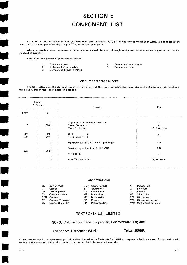
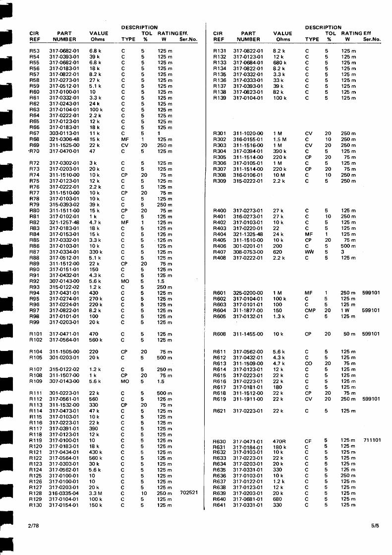
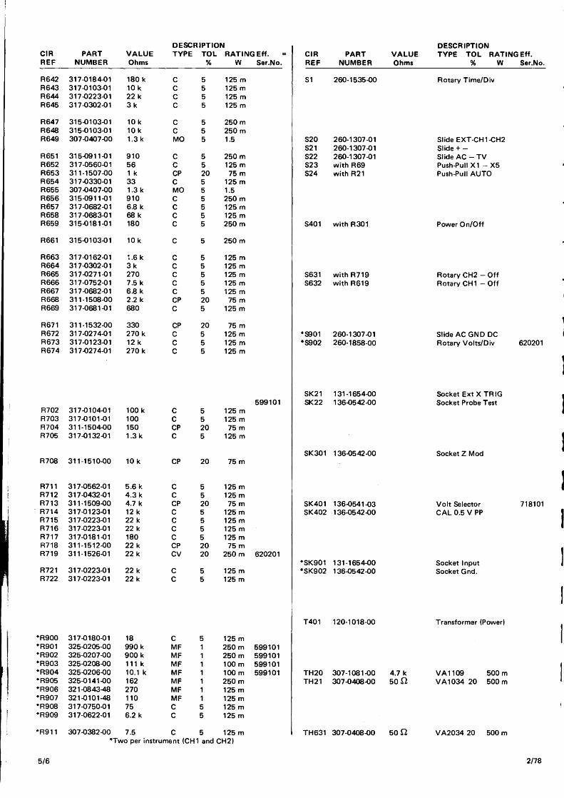
SECTION 5COMPONENT LIST
Values of resistors are stated in ohms or multiples of ohms; ratings at 70°Care in watts ~r sub-multiples of watts. Values of capacitorsare stated in sub-multiples of farads; ratings at 70°Care in volts or kilovolts.
Whenever possible, exact replacements for components should be used, although locally available alternatives may be satisfactory forstandard components.
Any order for replacement parts should include:
1. Instrument type 4. Component part number2. Instrument serial number 5. Component value3. Component circuit reference
CIRCUIT REFERENCE BLOCKS
The table below gives the blocks of circuit referer~es,so that the reader can relate the items listed in this chapter and their location inthe circuitry and printed circuit boards in Section 6.
CircuitReference
_______________ Circuit Fig.
Trig Input & Horizontal Amplifier 31 300) Sweep Generator 4
Time/Div Switch 2. 3 4 and 6
301 400 CRT ) 5401 600 Power Supply
Volts/Div Switch CH1 - CH2 Input Stages 1 A
Vertical Input Amplifier CH1 & CH2 1 B601 1000)
Y Amplifier 2
Volts/Div Switches 1A, lB and 6
ABBREVIATIONS
BM Button mica CMP Cermet preset PS PolystyreneC Carbon E Electrolytic Se SeleniumCP Carbon preset Ge Germanium Si SiliconCV Carbon variable MF Metal Film SM Silver micaCER Ceramic MO Metal oxide WW Wire-woundCT Ceramic Trimmer PE Polyester WWP Wire-wound presetCM Cermet thick film PP Polypropylene WWV Wire-wound variable
TEKTRONIX U.K. LIMITED
36 - 38 Coidharbour Lane, Harpenden, Hertfordshire, England
Telephone: Harpenden 63141 Telex: 25559.
All requests for repairs or replacement parts should be directed to the Tektronix Field Office or representative in your area. This procedure willassure you the fastest possible ~‘t~vice. In the UK enquiries should be made to Harpender,.
3/77 51
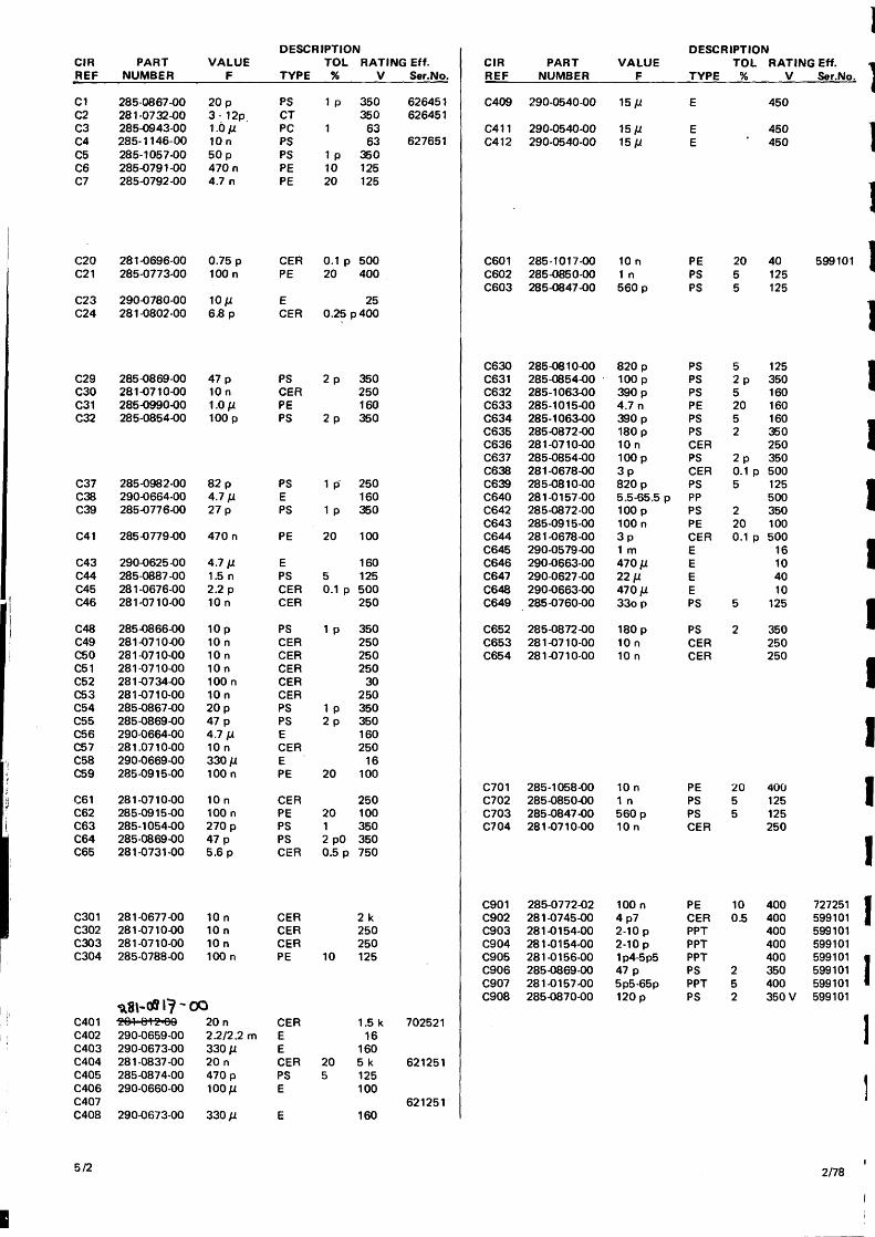
DESCRIPTION DESCRIPTION
C20 281-0696-00 0.75 pC21 285-0773-00 lOOn
C23 290-0780-00 10/2C24 281-0802-00 6.8p
,~8~-~I-ooC401 264—8t2~O9 20nC402 290-0659-00 2.2/2.2 mC403 290-0673-00 330/2C404 281-0837-00 20 nC405 285-0874-00 470pC406 290-0660-00 100/2C407C408 290-0673-00 330 p
CER 0.1 p 500PE 20 400
E 25CER 0.25 p400
C601 285-1017-00 iOnC602 285-0850-00 1 nC603 285-0847-00 560 p
C630 285-0810-00 82OpC631 285-0854-00 loopC632 285-1063-00 390 pC633 285-1015-00 4.7nC634 285-1063-00 390pC635 285-0872-00 l8OpC636 281-0710-00 iOnC637 285-0854-00 100 pC638 281-0678-00 3 pC639 285-0810-00 82OpC640 281-0157-00 5.5-65.5 pC642 285-0872-00 lOOpC643 285-0915-00 100 nC644 281-0678-00 3 pC645 290-0579-00 1 mC646 290-0663-00 470/1C647 290-0627-00 22/2C648 290-0663-00 470/1C649 285-0760-00 33o p
C652 285-0872-00 180 pC653 281-0710-00 iOnC654 281-0710-00 iOn
C901 285-0772-02 lOOnC902 281-0745-00 4p7C903 281-0154-00 2-lOpC904 281-0154-00 2-10 pC905 281-0156-00 1p4-5p5C906 285-0869-00 47 pC907 281-0157-00
5p5-65p
C908 285-0870-00 l2Op
20 4 599101
PE 20 400PS 5 125PS 5 125CER 250
PE 10 400 727251CER 0.5 400 599101PPT 400 599101PPT 400 599101PPT 400 599101PS 2 350 599101PPT 5 400 599101
PS 2 350V 599101
I
CIRREF
PARTNUMBER
VALUEF TYPE
TOL%
RATINGV
Eff.Ser.No.
Cl 285-0867-00 2Op PS 1 p 350 626451C2C3
281-0732-00285-0943-00
3-12p1.0/1
CTPC 1
35063
626451
C4 285-1146-00 10r~ PS 63 627651CS 285-1057-00 5Op PS ip 350C6 285-0791-00 470n PE 10 125C7 285-0792-00 4.7 n PE 20 125
CIRREF
PARTNUMBER
VALUEF TYPE
TOL%
RATINGV
Eif.Ser.No.
C409 290-0540-00 15/1 E 450
C411 290-0540-00 15/1 E 450C412 290-0540-00 15/1 E ‘ 450
C29 285-0869-00C30 281-0710-00C31 285-0990-00C32 285-0854-00
C37 285-0982-00C38 290-0664-00C39 285-0776-00
47 p10 n1.0/1100 p
82 p4.7/127 p
IPS
2p 350
CER 250PE 160PS
2p 350
PS ip 250E 160PS lp 350
PE 20 100
E 160PS 5 125CER 0.1 p 500CER 250
C4l 285-0779-00 470 n
I
C43 290-0625-00C44 285-0887-00C45 281-0676-00C46 281-0710-00
I
PSPSPSPEPSPSCERPSCERPSPPPSPECEREEEEPS
PSCERCER
5 1252p 3505 16020 1605 1602 350
2502p 3500.1 p 5005 125
5002 35020 1000.1 p 500
16104010
5 125
2 350250250
I
C48C49C50C5 1C52~53C54C55C56C57C58C59
285-0866-00281-0710-00281-0710.00281-0710-00281-0734-00281-0710-00285-0867-00285-0869-00290-0664-00281.0710-00290-0669-00285-0915-00
I4.7/11.5 n2.2 p10 n
10 p10 n10 niOn100 n10 n20 p47 p4.7/210 n330/1lOOn
10 n100 n270 p47 p5.6 p
10 n10 n10 n100 n
II
C61 281-0710-00C62 285-0915-00C63 285-1054-00C64 285-0869-00C65 281-0731-00
C301 281-0677-00C302 281-0710-00C303 281-0710-00C304 285-0788-00
PSCERCERCERCERCERPSPSECEREPE
CERPEPSPSCER
CERCERCERPE
CEREECERPSE
C7O1 285-1058-00 iOnC702 285-0850-00 1 nC7O3 285-0847-00 56OpC704 281-0710-00 10 n
ip 35025025025030
250ip 3502p 350
160250
1620 100
25020 1001 3502p0 3500.5 p 750
2k250250
10 125
1 .5 k16
16020 5k5 125
100
II
702521
621251
621251
5/2
E 160
2/78
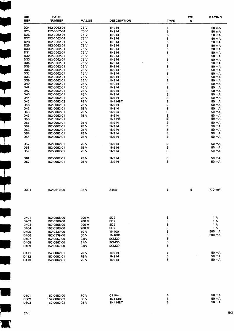
CIR PARTVALUE
TOL RATINGREF NUMBER DESCRIPTION TYPE %
024 152-0062-01 75V iN9i4 Si025 i52-0062-Ol 75V 1N914 SiD26 152-0062-01 75V 1N914 Si027 152-0062-01 75V 1N914 SiD28 152-0062-01 75V 1N914 SiD29 152-0062-01 75V iN9l4 SiD3O 152-0062-01 75V 1N914 Si031 152-0062-01 75V 1N914 SiD32 152-0062-01 75V 1N914 Si033 152-0062-01 75V lN9i4 Si034 152-0062-01 75V 1N9i4 Si t035 152-0062-01 75V 1N914 Si 50 mAD36 152-0062-01 75V 1N914 Si SOmAD37 152-0062-01 75 V 1 N91 4 Si 50 mAD38 152-0062-01 75V iN9l4 Si SO mA039 152-0062-01 75V 1N914 Si 5OmA040 152-0062-01 75 V 1 N9i 4 Si SOmA041 152-0062-01 75V iN914 Si 5OmA042 152-0062-01 75 V 1 N914 Si 50 mA043 152-0062-01 75V 1N9i4 Si 50 mA044 152-0062-01 75 V 1 N9i 4 Si SO mAD45 152-0062-02 75 V 1 N4148T Si 50 mA046 152-0062-01 75V 1N914 Si 50mA047 152-0062-01 75 V 1 N914 Si 50 mA048 1S2-0062-01 75 V 1 N914 Si 50 mA049 152-0062-01 75 V 1N914 Si 50 mAD5O i52006201 iN4l48 Si 50 mA,051 152-0062-01 75V 1N914 Si 50 mA052 152-0062-01 75V 1N914 Si 50 mA053 1S2-0062-01 75V 1N914 Si 50 mA054 152-0062-01 75V 1N9i4 SI 5OmA055 152-0062-01 75V 1N914 Si 5OmA
057 1S2-0062-01 75V lN914 Si SO mA058 152-0062-01 75 V 1 N914 Si SO mA059 152-0062-01 75V lN9l4 Si 50 mA
061 152-0062-01 75 V 1 N9i4 Si 50 mA062 152-0062-01 75 V ~N9i4 Si 50 mA
0301 152-0610-00 82 V Zener Si S 770 mW
0401 152-0566-00 200 V SD2 Si 1 AD4O2 152-0566-00 200 V SD2 Si 1 A0403 152-0566-00 200 V SD2 Si 1 A0404 1 52-0566-00 200 V SD2 Si 1 A0405 152-0339-00 50 V 1 N4001 Si 500 mA0406 152-0339-00 SO V 1 N4001 Si 500 mAD407 152-0567-00 3 kV SCM3O Si0408 152-0567-00 3 kV SCM3O Si0409 152-0567-00 3 kV SCM3O Si
0411 1S2-0O62-01 1N9i4 Si 50 mA0412 152-0062-01 1N914 Si SO mAD413 152-0062-01 1N914 Si 50 mA
Cl 104I ~.I A I AOT
0601 152-0483-00D602 152-0062-02 65 V
RATING
CIR PARTREF NUMBER
FB21 276-0597-00FB22 276-0597-00FB23 276-0597-00FB3O1 276-0597-00FB302 276-0597-00FS4O1 159-0077-00or 159-0079-00
L631 108-0482-00L632 108-0482-00
VALUE DESCRIPTION
Ferrite bead FX11SFerrite bead FX1 15’Ferrite bead FX11SFerrite bead FX115Ferrite bead FX1 15
Eif.Ser. No.
R22R23R24R25R26R27R28R29R3OR31R32
R34R35R36R37R38
R41
R42
R44
R48R49
R5iR52
317-0473-01317-0914-01317-0154-01317-0332-01317-0433-01317-0332-01317-0392-01317-0162-01317-0561-01311-1503-00317-0333-01
317-0682-01317-0392-01317-0103-01311-1858-00317-0330-01
317-0561-01 560317-0680-01 68
317-0682-01 6.8 k
317-0183-01 18k311-1512-00 22k
317-0103-01 lOk317-0512-01 5.1 k
RATINGw
C 5 125mC S 125mC 5 125mC 5 125mC 5 125mC 5 125mC 5 125mC 5 125mC 5 125mC 20 75mC 5 125m
C 5 i25mC S 125m
5C 5 125m
C 5 125mCP 20 75m
5 125m5 125m
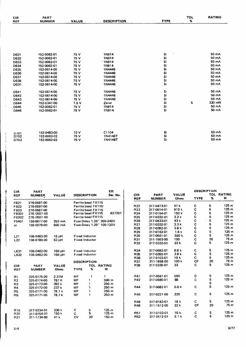
CIRREF
PARTNUMBER VALUE DESCRIPTION TYPE
TOL
0631 152-0062-01 75V 1N914 Si SO mAD632 152-0062-01 75V 1N914 Si 50 mAD633 152-0062-01 75V - 1N914 Si 50 mA0634 152-0062-01 75 V 1 N91 4 Si SO mAD635 152-0614-00 75 V 1 N4448 Si SO mAD636 152-0614-00 75 V 1 N4448 Si 50 mA0637 152-0614.00 75 V 1 N4448 Si SOmAD638 152-0614-00 75 V 1 N4448 Si SO mAD639 152-0614-00 75 V 1 N4448 Si 50 mA
D641 152-0614-00 75V 1 N4448 Si 50 mA0642 152-0614-00 75 V 1 N4448 Si 50 mA0643 152-0614-00 75 V 1 N4448 50 mA0644 152-0347-00 7.5 V Zener Si 5 330 mW0645 152-0062-01 75V 1N914 Si 5OmA0646 152-0062-01 75 V 1 N91 4 Si 50 mA
0/010702
152-0483-00152-0062-02
10 V75V
Cl 1041N4148T
SiSi
50 mA50 mA
0703 152-0062-02 7SV 1N4148T Si SO mA
DESCH IPTIONCIR PART VALUE TOLREF NUMBER Ohms TYPE %
627351
250 mA Fuse Delay 1 .25” 200-240V500 mA Fuse Delay 1.25” 100-120V
L21 108-0483-00 16 /1HL22 108-0780-00 53/AH
Fixed InductorFixed Inductor
Fixed InductorFixed Inductor
160 /2H160 /2H
47 k910 k150 k3.3 k43 k3.3 k3.9 k1.6k560 k10033 k
6.8 k3.9 k10 k100 k33
DESCRIPTIONCIR DART VALUE TOL RATINGREF NUMBER Ohms TYPE % W
AlR2A3A4R5R6
325-01 75-00325-0 1 74-00325-01 73-00325-0172-00325-0171-00325-0171-00
MFMFMFMFMFMF
C 5C 5C 5CP 20C 5
1 11 500m1 250m1 250m1 25Om1 250m
2.37M787 K392 k237 k78.7 k78.7 k
330 k150 k47 k
125 m125 m125 m
75 m125 m
R19 317-0334-01R20 317-0154-01R21 311-1734-00
C 5 125mC 5 125mCV 20 l5Om
R46 317-0221-00 220 C 5 125m
CC
5/4 8/77
CIR PARTDESCR IPTION
TOL RATING Eft.
R59R6OR6lA62R63R64R65R66R67R68R69
-R70
317-0512-01317-0100-01317-0332-01317-0243-01317-0104-01317-0222-01317-0123-01317-0183-01303-0113-01321-0306-48311-1525-00317-0470-01
5~i k103.3k24klOOk2.2k12k18klik15k22k47
CCCCCCCCCMFCVC
55555S5551205
i2Sm125m125m125ml2Sml25m125m125m1125m25Om125m
R72R73R74R75R76R77R78R79R8OR81R82R83A84A85R86A87R88R89R9OR91R92R93R94R95R96R97R98R99
317-0302-01317-0203-01311-1510-00317-0123-01317-0222-01311-1510-00317-0103-01315-0393-02311-1511-00317-0102-01321-1257-48317-0183-01317-0153-01317-0332-01317-0103-01317-0334-01317-0512-01311-1512-00317-0151-01317-0432-01307-0143-00315-0122-02317-0431-01317-0274-01317-0224-01317-0822-01317-0101-01317-0203-01
3k20klOk12k2.2klOklOk39 k15k1 k4.7k18k15k3.3klOk330k5.1 k22kISO4.3 k5.6 k1.2k430270k220k8.2 k10020k
CCCPCCCPCCCPCMFCCCCCCCPCCMOCCCCCCC
55205520552051555555205555555SS5
125ml25m75m
l25m125m75m
125m250 m75m
125 m125m125m125m125m125ml25m125 m75m
125m125 m1.5250m125ml2Sm125m125 mi25mi25m
R101R1O2
317-0471-01317-0564-01
470560k
CC
55
i25mi25m
R104Rl05
311-1505-00301-0203-01
22020k
CPC
205
75m500m
Al07A1O8R1O9
315-0122-02311-1507-00307-0143-00
1.2kik5.6k
CCPMO
5205
250m75m
1.5
AlliR112R113R114AilSRi16Ri17R118R119R12OR121Rl22R123Rl24R125A126R127A128A129R130
301-0223-01317-0561-01311-1532-00317-0473-01317-0103-01317-0223-01317-0391-01317-0123-01317-0100-01317-0183-01317-0434-01317-0564-01317-0303-01317-0562-01317-0100-01317-0100-01317-0203-01316-0335-04317-0104-01317-0154-01
22k56033047klOk22k39012k1018k430k560k30k5.6k101020k3.3M100k150k
CCCPCCCCCCCCCCCCCCCCC
5520S55555555555551055
500ml25m75m
i25m125ml2Sm125mi25mi25m125mi25m125m125mi25m125mi25ml25m25Oml25m125m
CIR PART
R137 317-0393-01 39k C 5 125rR138 317-0823-01 82k C 5 125rRl39 317-0104-01 lOOk C 5 125r
R30l 311-1020-00 1 M CV 20 250rR3O2 316-0155-01 l.5M C 10 2SOrR303 311-1516-00 1 M CV 20 250rR3O4 317-0394-01 390 k C S 125R3O5 311-1514-00 220k CP 20 75rR3O6 317-0105-01 1M C 5 l2SrR307 311-1514-00 220k CP 20 75rR3O8 316-0106-01 lOM C 10 2SOrR309 315.0222-01 2.2k C 5 250r
R400 317-0273-01 27k C 5 l25rR4O1 316-0273-01 27k C 10 250rA4O2 317-0103-01 lOk C 5 125rR4O3 317-0220-01 22 C 5 l25rR4O4 321-1325-48 24k MF 1 125rR4O5 311-1510-00 lOk CP 20 75rR406 301.0201-01 200 C 5 SOOrR407 308-0753-00 620 WW 5 3R408 317-0222-01 2.2k C 5 l2Sr
R60l 325-0200-00 1 M MF 1 250 nR602 317-0104-01 100k C 5 125nR6O3 317-0101-01 100 C 5 125rnR604 311-1877-00 150 CMP 20 1WA605 317-0132.01 1.3k C 5 125m
A608 311-1455-00 lOk CP 20 50m 5991
A611 317-0562-00 5.6k C 5 125mR612 317-0432-01 4.3k C 5 l25mR6i3 311-1509-00 4.7 k CO 20 75 mA6i4 317-0123-01 12k C 5 125mA6i5 317.0223-01 22k C 5 125mR616 317-0223-01 22 k C 5 125 mR617 317-0181-01 180 C 5 l25mR618 311-1512-00 22k CP 20 75mA6l9 311-1911-00 22k CV 20 250m 599~
R62l 317-0223-01 22k C 5 125m
R630 317-0471-01 470R CF S 125mR631 317-0184-01 180k C i25mR632 317-0103-01 10 k C 5 125 mR633 317-0223-01 22k C 5 125mR634 317-0203-01 20k C 5 125mA635 317-0331-01 330 C 5 125 mR636 317-0103-01 lOk C 5 250mR637 317-0122-01 1.2k C 5 125mR638 317-0123-01 12k C 5 i25mR639 317-0203-01 20k C 5 125mR64O 317-0681-01 680 C 5 l2SmR64l 317-0331-01 330 C 5 l25m
59~
711
2
DESCRIPTIONCIR PART VALUE TYPE TOL RATING Eft. =
REF NUMBER Ohms % W Ser.No.
R642 317-0184-01R643 317-0103-01R644 317-0223-01R645 317-0302-01
DESCR IPTIONCIR PART VALUE TYPE TOL RATING Eff.REF NUMBER Ohms % W Ser.No.
R647R648R649
R651A652R653R654R655R656R657A658R659
180 k10 k22 k3k
10 klOk1.3k
91056ik331.3 k9106.8 k68k180
315-0103-01315-0 103-0 1307-0407-00
315-0911-01317-0560-01311-1507-00317-0330-01307-0407-00315-0911-01317-0682-01317-0683-01315-0181-01
R661 315-0103-01 lOk
R663A664R665R666A667R668R669
317-0162-01317-0302-01317-0271-01317-0752-01317-0682-01311-1508-00317-0681-01
l .6 k3k2707.5 k6.8 k2.2 k680
330270 k12 k270 k
100 k1001501.3k
R671 311-1532-00R672 317-0274-01A673 317-0123-01R674 317-0274-01
R702 317-0104-01A703 317-0101-01R704 311-1504-00A705 317-0132-01
C 5 125mC 5 125mC 5 125mC 5 125m
C 5 25OmC 5 250mMO 5 1.5
C 5 250mC S l2SmCP 20 75mC 5 125mMO 5 1.5C 5 250mC 5 125mC 5 125mC 5 250m
C S 2SOm
C 5 125mC S 125mC 5 l25mC 5 125mC 5 125mCR 20 75mC 5 125m
CP 20 75mC 5 l2SmC 5 125mC 5 125m
C 5 125mC 5 l25mCP 20 7SmC 5 125m
CR 20 75m
C S l2SmC 5 125mCP 20 75mC S l2SmC 5 125mC 5 l25mC 5 125mCP 20 75mCV 20 2SOm
C 5 l2SmC 5 125m
C 5 125mMF 1 25OmMF 1 250mMF 1 lOOmMF 1 lOOmMF 1 25OmMF 1 125mMF 1 125mC 5 125mC 5 125m
R708 311-1S1O-00 lOk
Si 260-1535-00 Rotary Time/Div
S20 260-1307-01 Slide EXT-CH1 -CH2S21 260-1307-01 SlideS22 260-1307-01 Slide AC— TVS23 with R69 Push-Pull Xl — X5S24 with R2l Push-Pull AUTO
S401 with R301 Power On/Off
S631 with R719 Rotary CH2— OffS632 with R619 Rotary CH1 — Off
*S9O1 260-1307-01 Slide AC GND DC*S902 260-1858-00 Rotary Volts/Div
SK21 131-1654-00 Socket Ext X TRIGSK22 136-0542-00 Socket Probe Test
SK3O1 136-0542-00 SocketZ Mod
SK4O1 i36-0S41-03 Volt SelectorSK4O2 136-0542-00 CAL 0.5 V PP
*SK901 131-1654-00 Socket Input*SK9O2 l36-0S42-00 Socket Gnd.
T4O1 120-1018-00 Transformer (Power)
TH2O 307-1081-00 4.7 k VAl 109 500 mTH21 307-0408-00 SO~2 VA1034 20 500m
TH631 307-0408-00 SO~2 VA2O3420 500 m
R711R712R713R714R715R7 16R7 17R718R719
317-0S62-01317-0432-01311-1509-00317-0123-01317-0223-01317-0223-01317-0181-01311-1512-00311-1526-01
5.6 k4.3 k4.7 k12 k22 k22 k18022 k22 k
620201
718101
R72l 317-0223-01 22 kA722 317-0223-01 22 k
599101
620201
599101599101599101599101
*R900 317-0180-01 18*A90l 32S-02O5-00 990 k*R902 325-0207-00 900 k*R903 325-0208-00 lii k*R9O4 325-0206-00 10.1 k*A905 325-0141-00 162*A906 321-0843-48 270*R907 321-0101-48 110*R908 317-0750-01 75*R909 317-0622-01 6.2 k
*R9i1 307-0382-00 7.5 C 5 12S m*Two per instrument (CH1 and CH2)
5/6 2/78
CIR PART Eff.REF NUMBER DESCRIPTION TYPE Ser. No.
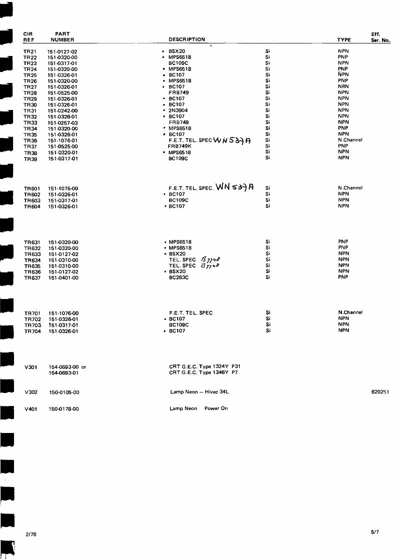
TR21 151-0127-02 • BSX2O Si NPNTR22 151-0320-00 • MPS6518 Si PNPTR23 1S1-0317-01 BC1O9C Si NPNTR24 151-0320-00 • MPS6S18 Si PNPTA25 151-0326-01 • BC107 Si ~4PNTR26 151-0320-00 • MPS6518 Si PNPTR27 151-0326-01 • BC107 Si NRNTR28 151-052S-OO FRB749 Si NPNTR29 1S1-0326-01 • BC1O7 Si NPNTR3O 151-0326-01 • BC1O7 Si NPNTR31 lSl-0242-O0 • 2N3904 Si NPNTR32 151-0326-01 • BC1O7 Si NPNTR33 151-0257-03 FF1B749 Si NPNTR34 151-0320-00 • MPS6518 Si PNPTR3S 151-0326-01 ‘ BC1O7 Si NPNTR36 151-1076-01 F.E.T. TEL. SPEC~itj /4 S~Z~fl Si N.ChannelTR37 151-0525-00 FAB749K Si PNPTR38 151-0320-01 • MPS6518 Si NPNTR39 1S1-0317-01 BC1O9C Si NPN
TR6O1 151 -1 076-00 F.E.T. TEL. SPEC. VJi\1 ~z9 1~ Si N.ChannelTA602 151-0326-01 • BC1O7 Si NPNTR603 151-0317-01 BC1O9C Si NPNTA604 151-0326-01 • BC1O7 Si NPN
TR631 151-0320-00 • MPS6518 Si PNPTR632 151-0320-00 • MPS6518 Si PNPTR633 1S1-0127-02 • BSX2O Si NPNTR634 1S1 -031 0-00 TEL. SPEC Si NPNTR635 151-0310-00 TEL. SPEC Si NPNTR636 151-0127-02 • BSX2O Si NPNTR637 151-0401-00 BC263C Si PNP
TR7O1 lSi-1O76-00 F.E.T. TEL. SPEC Si N.ChannelTR7O2 151-0326-01 • BC1O7 Si NPNTR703 151-0317-01 BC1O9C Si NPNTR7O4 151-0326-01 • BClO7 Si NPN
V301 154-0693-00 or CRT G.E.C. Type 1324V P31154-0693-01 CAT G.E.C. Type l346Y P7
V302 150-0105-00 Lamp Neon — Hivac 34L 620251
V401 150-0178-00 Lamp Neon Power On
2/78 5/7
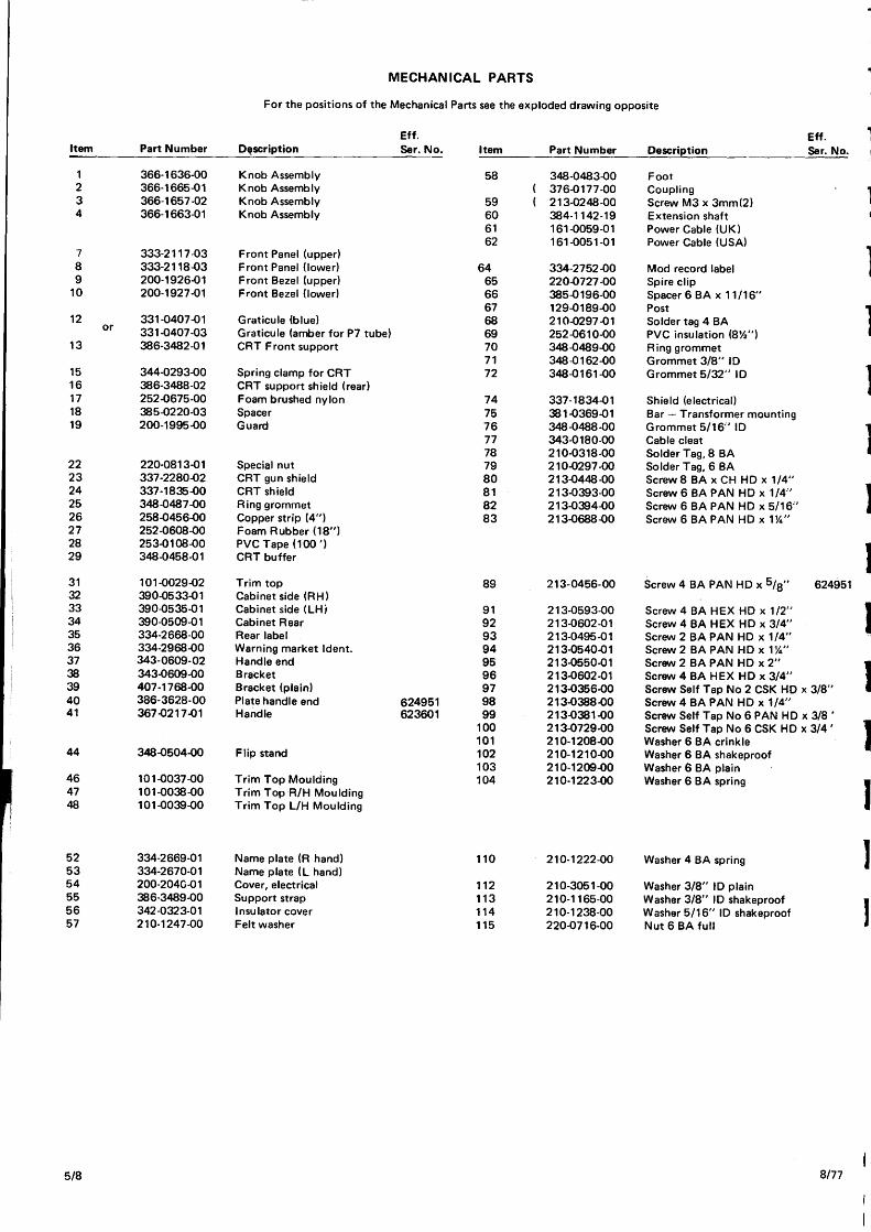
MECHANICAL PARTS
For the positions of the Mechanical Parts see the exploded drawing opposite
366-1636-00366-1665-01366-1657.02366-1663-01
333-2117-03333-2118-03200-1926-01200-1927-01
331-0407-01or 331-0407-03
386-3482-01
344-0293-00386-3488-02252-0675-00385-0220-03200-1995-00
Knob AssemblyKnob AssemblyKnob AssemblyKnob Assembly
Front Panel (upper)Front Panel (lower)Front Bezel (upper)Front Bezel (lower)
Graticule (blue)Graticule (amber for P7 tube)CAT Front support
Spring clamp for CATCRT support shield (rear)Foambrushed nylon.SpacerGuard
58 348-0483-00376-0177-00
59 ( 213-0248-0060 384-1142-1961 161-0059-0162 161-0051-01
64 334-2752-0065 220-0727-0066 385-0196-0067 129-0189-0068 210-0297-0169 2S2-0610-0070 348-0489-0071 348-0162-0072 348-0161-00
74 337-1834-0175 381-0369-0176 348-0488-0077 343-0180-0078 210-0318-0079 210-0297-0080 213-0448-0081 213-0393-0082 213-0394-0083 213-0688-00
FootCouplingScrew M3x 3mm(2)Extension shaftPower Cable (UK)Power Cable (USA)
Mod record labelSpire clipSpacer 6 BA x 11/16”PostSolder tag 4 BAPVC insulation (8W’)Ring grommetGrommet 3/8” IDGrommet 5/32” ID
Shield (electrical)Bar — Transformer mountingGrommet S/16’ IDCable cleatSolder Tag, 8 BASolder Tag, 6 BAScrew8 BA x CH HD x 1/4-’Screw 6 BA PAN HD x 1/4’Screw 6 BA PANHOx 5/16”Screw 6 BA PAN HO x 1Y
4”
Eif.Ser.No.
31 101-0029-0232 390-0533-0133 390-0535-0134 390-0509-0135 334-2668-0036 334-2968-0037 343-0609-0238 343-0609-0039 407-1768-0040 386-3628-0041 367-0217-01
Trim topCabinet side (RH)Cabinet side (LH,Cabinet RearRear labelWarning market Ident.Handle endBracketBracket (plain)Plate handle endHandle
91 213-0593-0092 213-0602-0193 213-0495-0194 213-0540-0195 213-0550-0196 213-0602-0197 213-0356-00
624951 98 213-0388-00623601 99 213-0381-00
100 213-0729-00101 210-1208-00102 210-1210.00103 210-1209-00104 210-1223-00
112 210-3051-00113 210-1165-00114 210-1238-00115 220-0716-00
Screw 4 BA HEX HO x 1/2”Screw 4 BA HEX HOx 3/4”Screw 2 BA PAN HO x 1/4”Screw 2 BA PAN HO x 1W’Screw 2 BA PAN HO x 2”Screw 4 BA HEX HO x 3/4”Screw Self Tap No 2 CSK HO x 3/8”Screw 4 BA PAN HO x 1/4”Screw Self Tap No 6 PAN HO x 3/8’Screw Self Tap No 6 CSK HO x 3/4’Washer 6 BA crinkleWasher 6 BA shakeproofWasher 6 BA plainWasher 6 BA spring
Washer 3/8” ID plainWasher 3/8” ID shakeproofWasher 5/16” ID shakeproofNut 6 BA full
Item Part Number DescriptionEff.Ser. No. Item Part Number Description
234
789
10
12
13
1516171819
2223242526272829
220-0813-01337-2280-02337-1835-00348-0487-00258-0456-002S2-0608-00253-0108-00348-04S8-Oi
Special nutCATgun shieldCAT shieldAing grommetCopper strip (4”)Foam Rubber (18”)PVC Tape (100’)CAT buffer
89 213-0456-00 Screw 4 BA PAN HID x 624951
44 348-0504-00 Flip stand
46 101-0037-00 Trim Top Moulding47 101-0038-00 Trim Top R/H Moulding48 101-0039-00 Trim Top L/H Moulding
52 334-2669-01 Name plate (A hand)53 334-2670-01 Name plate (L hand)54 200-2040-01 Cover, electrical55 386-3489-00 Support strap56 342-0323-01 Insulator cover57 210-1247-00 Felt washer
III
110 210-1222-00 Washer 4 BA spring I1
5/8 8/77
(4(~ t.)t’)
(di
0t
(0
-~ ±~1/j±~..
InC)
:~~(diO
1’I: ~
L.262728
12 3
100
MECHANICAL ASSEMBLY
1YP~CALSLIDER SWITCH
COVER FRONI p~~1ECflON
VOLTSID(VSWITCH
44
113
D61A
C
SECTION 6
CIRCUIT DIAGRAMS
To minimise the risk of misinterpretation of component values on circuit diagrams, the decimal point has been replaced by the multiplier orsub-multiplier of the basic unit. For instance, 2.2 megohms is shown as 2M2 and 1.8 picofarads is shown as 1p8.
To aid the reader further, in addition to the block Circuit Reference Table in Section 5.1, to locate a component in the circuit diagrams, atable is provided at the top, in which the circuit reference will appear, where practicable, directly above the component being sought.
10/7S
RESISTOR~_J900902903 904
602 603 604 621605
601
906905907
619909608 908
CAPACITORS J 901 905 ——--.----——-—.— 601
902 903 904 906 907 908 _________________ ________________ _____________________________ .~_ ___________________MISC JSK901-902 5901 5902-iR
*901
5902—iF . DSO1 TR6O1 S902-2R
volts/div.
NOTES.1. 168/1 DENOTES PC. BOARD/ EYELET OR TERMINAL N
2CONNECTION.
2. * DENOTES COMPONENTS NOT MOUNTEDON PC. BOARD.3. SWITCH ~ SHOWN IN FULLY ANTICLOCKWISE POSITION.
VOLTS/DIV SWITCH CH1-CH2INPUT STAGESD61A, FIG.1A. MK2
PC.168
FRONT PANEL MARKING.
R 90018R
INPUT
D.C.
OND.
*
5902-iR
*
C9024p
7
F~f
TO
156/39FIG.1 B
TO 156/26 CH1156/62 CH2FIG.1B
5K902
*R6O11 MO
TOI5G/C3 CHI156/C330-42FIG.1 B.
5V TO156/67FlG.1B
.2
~
21(
5%~ llOn*
— — — — — — — —
FRESISTORS I611
CAPACITORS
IR 602
602
TR603 0602
614612613
603
D603 TR604
1~LIoE~EH2pS/div.
616 618615
617
711
TR 702
702
712713
IR 703 0702 0703 TR7O4
LrEE-2.i.IS/di~
NOTES.1. * DENOTES COMPONENTS NOT MOUNTED ON PC. BOARD.Z 156/26 DENOTES PC. BOARD! EYELET OR TERMINAL N2. CONNECTION.a ALL WAVEFORMS NEASURED WITH CAl. WAVEFORM FED 10 BOTH CHANNELS.
VOLTS/DIV SET TO 0.1 TRIG ..LECTOR TO CH1 AND TIME/DIV TO 2m5.
VERT INPUT AMPLIFIER CH.1 D61AFIG.1B PC. 156 Mk2
VERT INPUT AMPLIFIER CH.2 D6IAFIG.1B PC.156~2
-1-13V FROMJUNCTION OFC643 &R 656FIG 2VAMP
IR
714 716715
722 717703
718
-i-7.5V FROMTHE WIPER OF
FIG2 R668FIG.2YAMP
704
Si-1R
0.6V
~2.pJ~fr2
5mS/div
JUNCTION
FROM WIPEROF R619 CH1VOLTS! DIV
~FLE~-—0V
- FIG.5
2L
IRESISTORS 669 631632
672 634673
644 633 639 642630 641 643
635 636637
674638
640
CAPACIT~~~] 631 649 630635
632 633 634652
639
640 637 654653
636
MISC. jI
L632SI-2F
$631 D632
TR631
0645 0631
TR632SI-2F
0633 D646
L6310634
$632
(P05,2 to 211 23
CH.2.
156/21
C631loop
NOTES.
I. W DENOTES COMPONENTS NOT MOUNTED ON P.C. aOARD.
2. 56/55 DENOTES P.C. BOARD/EYELET OR TERMINAL No. CONNECTION.
3 ALL WAVEFORMS MEASURED WITH CAL WAVEFORM FED TO BOTH CHANNELSVOLTS/DIV SET TO 0.1 TRIG SELECTOR TO CH.I AND TIME/DIV TO 2rnS.
r~ +60V22 I
~ TIME/DIV.\ SI-2F
(POSt)
1
22
(POS. 11 to 21) I
+80V
OFF
56/90
+22V ~1~E2jiS/dtv
1 ~+22V \_.~_j .7V
S /div
2/78
661 647653 b63
649 652645 651
648
645 638642 646641 648
654 655671 658 656
665 668667666
647 644
‘rR636 TP~33 TR634 TH631 TR6350635 0638 D643 D641 TR637
D637 D636 D639 D642 D644
657 659
FROM FROMTR6O2 C6O3/COL. P614
CHI.F 1G.IA
FROMTR7O2 C703/COL. P714
~.1Y.
CH.2.FIG lB
— 7-SVTO R49 TRIG.INPUTFIG.3 10 R24 FIG.4SWEEP GEN. TO R619Fl014 & R719 FIG. lBVERT INPUT AMP
- 13V
FROM POWER SUPPLYFIG.5 205/19 VIA.156/97
‘Y’ AMPLIFIER— D6LA
664
643
FIG.2. ~4/77
I[RESISTORS I 23
37 3238 46 49
34 44 48
120121122
25 126 52 -
CAPACITORS
2120 51
3 30
MISC. TH2O TR23FB23 024
TH2ID26 027
TR25D28 031
SK2I $20 SI—IFD25
51-IR 521D29
III
I
TH2O
41(7
CI-4.2. TRIG. SIGNALFROM $902 2F FIGIB
CH.I.~_CH.I.TRIG. EXT.SIGNAL o
1~
FROM S9022F FIG.IA
SK2I
EXT. XTRIG.
SOD
loo
200
5O0~&,.,
extch 2
FRONT PANEL
~5O ~~2O
110
12
MARKING
II
NOTES.I. * DENOTES COMPONENTS NOT MOUNTED ON P.C. BOARD.
2. 156/Cs DENOTES PC. BOARD/EYELET OR TERMINAL No.CONNECTIO3. SWITCH SHOWN IN FULLY ANTI-CLOCKWISE POSITION.
4. FOR Si SWITCH WAFERS SEE FIG.6.5. ALL WAVEFORMS MEASURED WITH CAL WAVEFORM FED TO BOTH
CHANNELS VOLTS/DIV. TO 0-I TRIG SELECTOR TO CH.I ANDTIME/DIV TO 2mS. I
I
FROM JUNCTIONC643/R656 -
FIG.2 V-AMP
+1
P121
4301K
R52
JC51 •~K~1~ I
FROM R55156/13 FIG.3
CH.2.
I
D3I
U
IFROM
D644/ R668FIG.2 U
JO?
1~)b7
Sm S/div.
R48
U
C 20
Op75
J
—7~5VFROM
C648/C647FIG. 2 I
53 805657
23
TR26032 054
D33D35
+110V
55 66 6883 64
6569
24 90
D55D34D37
5655
58
S23
P124
FROM C643/R656FIG. 2 VAMP+13V
53
R8922K
3V—+~J.~2~5V
SmS/div
FROM JUNCTION RIO5. D47 156/9C FIG.4
—13VFROM 205/19POWER SUPPLYFIG. 5 VIA.156/97
TRIG INPUT & HORIZONTAL AMP D614FIG.3.
9989
76 82
70
79 92Bi 93
94
53
98
104 109
107108
D41TR3I
D42
III112113
45
TR33D44
44
TR37
TO C.R.T.FIG.5
TO C23SWEEPGEN.FIG. 4
TOSi 1RFIG.3
‘—13V —13V
22 24 25 27 2826
59 24
23
135 29 35 36 413142~0
29
TR22 L21 TR24
S1—ZF L22
51 ‘36 137 138 139
32 64
‘—---l
D30 TR3O D62D 61
II
U5
POS, 18.15 1020
U
ins I0~
200
loo
2000
500ext
cli 2
FRONT PANEL
~5O$20
$10
I
MARKING
IJS NOTES
I. * DENOTES COMPONENTS NOT MOUNTED ON PC. BOARD.2. 156/6C DENOTES PC. BOARD/EYELET OR TERMINAL No.CONN.
3. SWITCH SHOWN IN FULLY ANTI-CLOCKWISE POSITION.
4. FOR SI SWITCH WAFERS SEE FIG.6.
5. ALL WAVEFORMS MEASURED WITH CAL. WAVEFORM FED TO BOTH
CHANNELS. VOLTS/DIV. SET TO O~l.AND TRIG. SELECTOR TO
CIII. AND TIME/DIV. TO 2mS.
6. PUSH PULL SWITCH S24 IS SHOWN IN THE OUT POSITION
RESISTORS
21 19
CAPACITORS
MISC.
S24S 22a
I
127 126 130 132 134129 131 133
6263 61
I
1R21 TR 38 057 TR39 S22b
056 058 059
65
+rv-t- 13V
JiOOnR28
+13V
R36lOK
TRIG.
LEVEL
R21” 47K
ITI~156/25 I
IIK
T
IIR139
— 7V5FROM
C648IC647FIG 2 ‘YAMP
L
I
680 K
R2643K
~3V
SI
—~--J
tim2/ division
UIIIU
84 88 6 72 lOl 105 114 95 115 102 96 97 91 54 8685 5 I 75 116 62 87
6) 4 77 73 117 58 677863
32
74 118 5960 119
2 3 4 S 7 6 43 38 5752
D36 052SK22 045
TR3 4TR27
PROBETEST ~
51(22
I56/S3
R78lOK
39 54 41 3749 48
D53 S)-2R SI-3P 046 SI-3FTR36 D47
0391R29
D48 051
0V 1 1~ 06V +110V
5rnS/div ‘BETWEEN JUNTION RIO) R)O5
& EYELET 156/56 20K SmS/divTO P89 156/9C /
047 048
R88SKI
‘I045 I r T~-- ‘T~ --
~CI* ~C3~~.iopJ
10* ~‘~°_L~
~6-30p ~ IOn C48.~R84 I •C~ (Op
15K _______ r—~ T 50~TO C635 (POS 3 IC 8) PC’S.9 to 14)
FIG.2. - ~
t — (POL ,2j 3 ~ -
1~- ~
P85
31(3
036
i_I ,fD52~
)POS9 14.2C,21)1
78K7 (POS 7,~6,1..5 6~ 3S~
237K )POS~12nfl9)4
Ii PC.4.~C1E,1’”2~ I
::~: 9 16)
2M37
~ ~D53
P6)3K3
6V ~ 1
Sm S/div
P63OOK
- 13V-~
TRACER77 lOK LENGTH
-V° ~i ~~ t_l- ~OV
P723 KO
-13V-~
47K
C54
-It--2Op
51*3F
JOIPOS 9
(* ?~~C7 PC.53
4n7J 8)
C647~0
D39’
046
&Io~R75
2K
R7320K
+ 110V
R95270K
i-13 V
PIlSlOK
R102560K
SO 46
049 S24
TR3S 050
4 110V
R96<220K
LI049
C 46IOn
(4/\.D50
]
040038
TR32TR 28
043
+117V FROM1 POWER
+ 110V +110V~5UppLy
C 38
-10---
C3t7
-II--82p
OR IBOp
P914K3
040
-I4-~
P58.27K
c-i038
-$-
-4- +13VFROM P656
FIG. 2‘Y’AMP
80V
Sm S/div
156/7C
TO CR1F)G.5I 9t o~
.4~v ~ 4Q1, ,
- SKI I .1..)2Om S/div
/ 156/C7~Pll6 /
22 TOJUNC
~~4~37 C632- _-a~’~~’~~
TR28~5617
56/0
~RlI7 C41 P86390R — lOK
47On
043TR3S ,P3051
P9781(2156/47 R54 P87
12K 39K 330K
AUTO S24
I0n~~- 156/97 ~3V
i-’- -0V3V /
t-.L~ L5mS/div P118
~79 ___-.—13V-4—
6V ....‘ -
lOm S/div
FROM PO9~ER
SUPPLY FIG 5
SV +13V 205/19
lOinS/dIv
SWEEP GENERATOR D6IA
- 13V
C 52
~OI
.-
FIG. 4.
~SIST0RS 402 403
401
404 400405
406407408
CAPACITORS! 401 402 403 404 405 406 408
Misc. SK4O1FS4OI
T401 040104040405
04020403
D408 0409D4l1
0412
0413 SK4O2
5401 0406 0407 V4OI I
SK4OI
205/2 2 S4OI
205/21 205/23 25OmA o 117V I9107V I
I IPOWERON/OFF I
0V I..)
205/25
205/2 7205/24
E
P.C. 205
NUIES.
I. * DENOTES COMPONENTS NOT MOUNTED ON P.C. BOARD.
2. 156/2 DENOTES PC. BOARD/EYELET OR TERMINAL No. CONNECTION3. ALL WAVEFORMS MEASURED WITH CAL. WAVEFORM FED TO BOTH
CHANNELS. VOLTS/DIV. SET TO 0-I. AND TRIG. SELECTOR TO CH.I.
AND TIME/DIV. TO 2m5.
~~~~~~~1
I
TOC.R.To4 (PD-A.)
5mS/div
- 7~5VFROM C648/C647
FIG. 2 ~YAMP
IIII
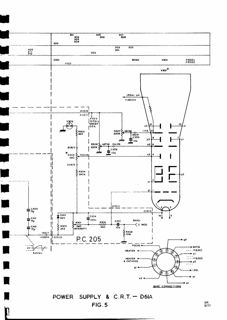
409411412
309
301 305 307302 306 308303304
302 30330$
SK3O1 V301 FB3OI
V3O2 FB302
V3OI~
— —I— — — — —
~~~0
II
II
0301
—
+ 2500V
Ii
xl
304
-~ISm S/div.
P.C. 205HEATER
&
MOD
--j
*2
BASE CONNECTIONS
al
- ASTIG
I.R.S.
xl
POWER SUPPLY & C.R.T. D6IA
FIG.55R8/77
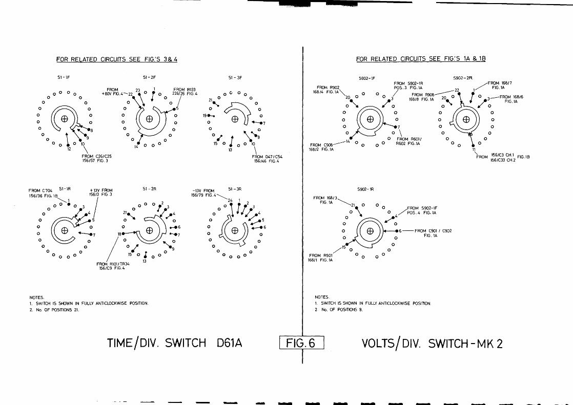
FOR RELATED CIRCUITS SEE FIG.S 3&4 FOR RELATED CIRCUITS SEE FIG.S 1A & lB
51-iF
00000 0
0 0
000 ~
0 0 10
12 \FROM C26/C25156(57 FIG. 3
Si -2F
R133FIG .4
Si - 3F
oO 00Oo
19—,
0
0 0o,?\~.9
15 0 ~ 0 ~ 10
13 \FROM D47/C54
156/46 FIG.4
5902 —1F
FROM R902
)68/4 FIG.1A\ ~ 0 0
~5II~~o\0 0 FROM R601/
FROM C90B-~~4
~ 0 0 ~ R6O2 FIG.IA168/2 FIG.1A
FROM 5902-IR
POS.3. F)G.1A
0 3/ FROM
168/8 FIG.1A
59O2—2R ,-FROM 168/7
~ FIG.1A
03
_._FROM 168/6
FIG. 1A
0
0
0
0
l56/C3 CH,1 FIG lBl56IC33 CH.2
FROM C 704 Si -1R +13V FROM156/36 FIG.1B 156/3 F)G.3
oO•o3
I0
4/0
0
0 00000
FROM R101/TR34156/C9 FIG.4
Si —2R Si —3R-13V FROM156/79 FlG.4—.~
OO°’~tf~.4
0
0 4~—6
O 0
O
o o0
0000
NOTES.1. SWITCH IS SHOWN IN FULLY ANTICLOCKWISE POSITION.
2. No. OF POSITIONS 21.
TIME/DIV. SWITCH D61A
NOTES.
1. SWITCH IS SHOWN IN FULLY ANTICLOCKW)SE POSITION.
2. No. OF POSITIONS 9.
0
0
0
0
0
0
0
0
00
000
0
0
0
0
0
0
o0 0
Oo0
0
00
5902—iR
FROM 168/3..~~FIG. 1A \ 0 0 0 FROM S902-IF
0 0 ,-~‘P0S.4 FIG.lAO
~ C9OI / C902FIG. 1A
0
V~0 0FROM P901 0 o 0
168/1 FIG. IA
VOLTS/ DIV. SWITCH - M K 2
— ~
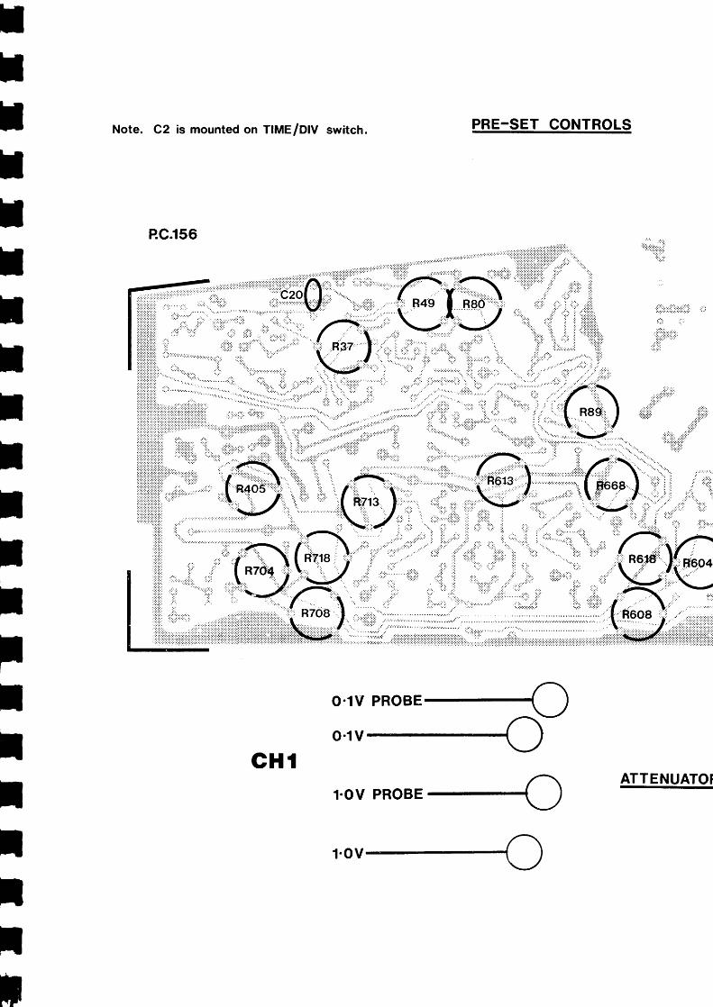
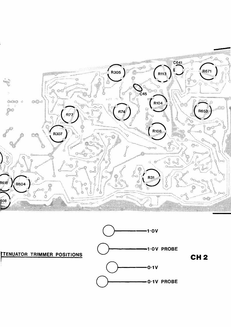
1101 U
C45 .a
C)
FOV
—1-0V PROBE
IITENUATOR TRIMMER POSITIONS CH 2
0-1V
0 0-1V PROBE

K
I
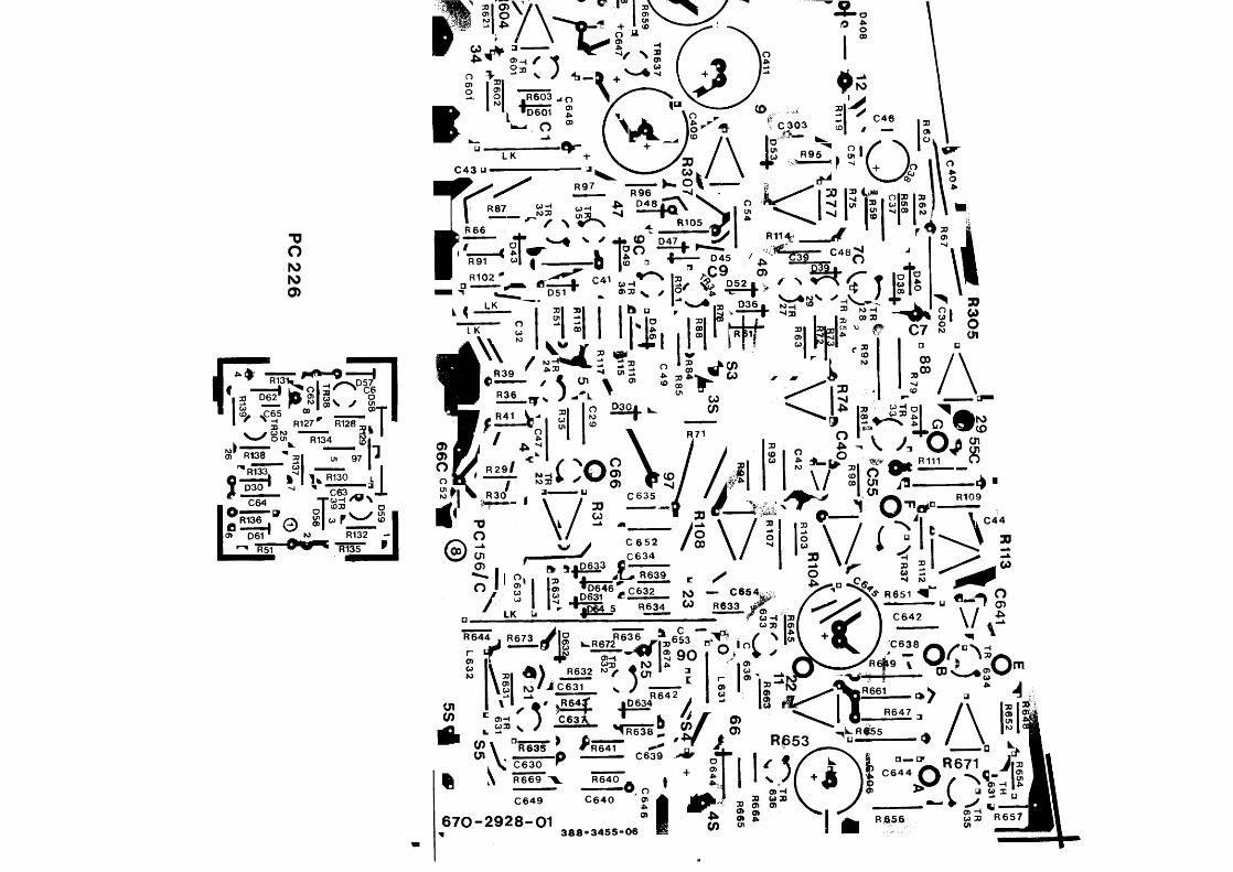
Ç ~ :i~’~ç~ ~ I
~ .,, .5 3 ~1—~ ~
~. ~ ~
~ f~ 1LJ ,•~ ~ ~ C303
K ~~1
- ‘~%%5
.5
..:~Ø::Z/ \ .I~~~95-~q
~ _ L~
~ ~tr:5~i~i~î~~: __~ ~c C41 ~ ~
LK U ~ ~ ~____ -. ~t, r~I~1.LIK ~ ~ I
~ °‘I IR1
F ~-~--~ ~ ~f ~ R71
.C~f~tr%#,#4
O% I I~,M-~ t~J~,) ~ I lb
‘ C) -...iIC 635
~_
___ i~— 1~ ‘~79~ ~.L9i~? C
L~ 41.~ R639~ ____~ •D631 ~ ______
~ R
a)a)C) P29l0
~i .~I
-I010)~5- I I
Ci(.3I.LK L~
~r6~30~
~ I”~ ~ ~, ~9 ~)1JC631 45 IU’ ~ ,Y’~ ~b ~f(I) ~ C631,. ___~• — __ —
UI —C639.~’‘ ~
C630 P~\ R669I ____
670-2928-01I
C649
C-)Al~.)
U
.-&
C7U
L\.
_‘‘45 111 ~‘iW4 Rili ~)
0’ —
Ul~1 —L)
01OR109
—\~C44
U
C)0
\/ ~ ______
l~,\/ ‘~r / •~~:Q~c65.R651
~ 6 ~2” C642
(.373 Ci _____~ +
-~ ~ A
j~R661~ U
LR655
R653 ~‘U—
I ___73 (.573
01 _____0505
U’
____ ___ 0)
____ I +C640 ~
388e345506 (I)
C)F.5)F’.)a)
00‘.3
C644O~6~> I -J~~’
_____—bk ~R65.6

SECTION 7STANDARD OPTIONS
If the standard D61A instrument to which this Manual applies has been sUpplied with one or more of the Standard Options listed below,the appropriate technical data must be used in conjunction with the standard manual information.
Option 1 BNC Sockets for CH1 & CH2 inputs replaced by 4mm round black sockets (Par Number 136-0542-00)
Option 4 P7 CRT (Part Number 154-0693-01) fitted in place of standard Pil tube.
Option 6 For operation on 115V line voltage and fitted with USA power cord (Part Number 161-0051-00).