technology education electronics/digital
TRANSCRIPT
TECHNOLOGY EOUC!'~TION
Grades 9-12
Electronics/DigitalPROGRAM/COURSE
Draft for field test and orientation use duringJ the 1985-86 school year.

I
INDUSTRIAL ARTS EDUCATION Module of Instruction
PHASE - Concentration ELEMENT - Technology
AREA OF CONCENTRATION: Electronics
MODULE: 7.0 Digital Electronics
SUB-MODULE: 7.1 Binary Logic
TOPICS: Logic Gates Combinational Logic
PREREQUISITES: None
Prepared by
Howard Sasson George Legg
Robert F. Caswell James Goldstine Joseph Sarubbi
Sandra P. Sommer Bruce G. Kaiser
Reprinted 1998TOTAL TEACHING TIME: 30 Hours (8 Weeks)j

THE UNIVERSITY OF THE STATE OF NEW YORK Regents of.The University
CARL T. li.AY'DEN, Chancellor, A.B., J.D. ............................................................ Elmira .i>IANE O'NEILL MCGIVERN, Vu:e Chancellor, B.S.N., M.A., Ph.D.................... Bayside J. Eow.ARD MEYER, B.A., LL.B. ..............................•••..•..........•........................... Chappaqua R. CARLOS CARBALLADA, Chancellor Emeritus, B.S. .......................................... Rochester ADELAIDE L. SANFORD, B.A., M.A., P.D. ............................................................. Hollis SAUL B. COliEN, B.A., M.A., Ph.D•••....•.....~~---····················································· New Rochelle JAMES C. DAWSON, A.A., B.A., M.S., Ph.D. ..............•.......••..•..........•.......•..••••••.. Peru. ROBERT M. BENNEn, B.A., M.S. · .•...................................................................... 'Ibnawanda ROBERT M. J0IIN'S0N, B.S., J.D. •.•••....•....................•...•...•••..•.....................•..•.••. Lloyd Harbor PETER M. PRY'oR, B.A., LL.B., J .D., LL.D. ................•....................................... Alban.y .ANmONY' S. BO'l"l'AR, B.A, J.D. •.•••......•.....•............•.•••.•...••..•.••........•.........•••••..• Syracuse MERRYL H. TISCH, B.A., M.A ••..•••••...••...................•......................................•...• New York HAROLD 0. LEVY, B.S., M.A. (Oxon.), J.D. ......................................................... New York ENA L. FARLEY', B.A., M.A., Ph.D. ••.•..•.•......•..........•....••..•.••••..•...............•...••••••• Brockport GERALDmE D. C~EY, B.A., M.A., Ed.D ........................................................... Belle Harbor RIC.ARDO E. OQUENDO, B.A., J.D. .............................•......................................... Bronx
President ofThe University and Commissioner ofEducation RICHARD P. Mn.Ls
Chief Operating Officer ~ICHARD H. CATE
Deputy Commissioner for Elementary, Middle, Secondary, and Continuing Education JAMES A. KADAMUS
· Coordinator of Curriculum and Instruction ROSEANNE DEFABIO
-
The State Education Department does not discriminate on the basis of age, color, religion, creed, disability, marital status, veteran status, national origin, race, gender, genetic predisposition or carrier status, or sexual
,entation in its educational programs, services, and activities. Portions of this publication can be made avail- .Jle in a variety offormats, including braille, large print or audio tape, upon request. Inquiries concerning this
policy of nondiscrimination should be directed to the Department's Office for Diversity, Ethics, and Access, Room 152, Education Building, Albany, NY 12234.

INDUSTRIAL ARTS EDUCATION MODULE OF INSTRUCTION
PHASE - CONCENTRATION ELEMENT - TECHNOLOGY AREA OF CONCENTRATION·- Electronics MODULE - Digital Electronics SUB-MODULE - Binary Logic TOPICS:
Logic Gates Combinational Logic
OVERVIEW OF SUB-MODULE
DESCRIPTION
This is the first of two sub-modules in Digital Electronics covering the topics of decision-making Logic Gates and Combinational Logic circuits. The student will be exposed to digital signals, number systems, gate symbols and truth tables· necessary for the complete understanding of digital circuits and systems found in home and commercial electronic equipment. Topics are arranged to progress from basic concepts to the more advanced theories and applications. ·
It i_s suggested that a student may satisfactorily complete the Applied Electronics Math module (1.0) as a foundation for this sub-module.
GOAL
Upon the completion of both topics in this sub-module, the student will develop the necessary background knowledge and skills that are required to work with basic logic gates and apply their operational functions to combinational logic circuits. The teacher is to incorporate safe working practices and highlight related careers appropriate to each topic during instruction.
Provisions are made within the topics for the student to apply mathematical concepts and to develop positive work related attitudes.
- 1

MODULE - Digital Electronics SUB-MODULE - Binary Logic
Estimated Teaching Time
Logic Gates 15 Hours (4 Weeks)
Combinational Logic 15 Hours (4 Weeks)
Prerequisites
None
Emphasis
The content of this sub-module should reflect applications of current digital electronics technology and include experiments with newly emerging technology. Emphasis is to be placed on the identification, function and use of basic decision-making logic gates in digital electronic systems.
The estimated teaching time includes both instruction and safe laboratory hands-on activity for each topic in this submodule. ·when planning instruction, this time estimate should be adjusted according to the student's background, experiences, acquired competencies and laboratory facilities available. Attention should also be given to special student populations to be served.
-~ ... - ..
- 2

MODULE - Digital Electronics SUB-MODULE - Binary Logic
j
COMPETENCIES TO BE DEVELOPED
Upon satisfactory completion of this sub-module, each student should have acquired the following competencies:
1. Know and apply the concepts relative to accident cause and prevention in the electronics laboratory, and develop a positive attitude towards safe behavior and practices in the use of tools, machines and equipment.
2. Know and accurately identify a digital signal and examples of digital devices and systems.
3. Be familiar with families of digital integrated circuits, specifications and packaging.
4. Be capable of interpreting basic graphic symbols and schematics for digital logic gates, and test-operating a simple logic circuit using an integrated circuit(s) and appropriate power supply.
5. Be capable of interpreting and converting between binary and decimal number systems.
6. Know and apply the fundamental Boolean expression and representative truth table to the operation of basic logic gates and combinational logic circuits.
7. Be capable of safely using common digital test equipment to analyze circuits and components, and verify the principles binary logic.
8. Be familiar with common number systems used to implement encoding, decoding and arithmetic functions in digital circuits and systems.
9. Know and accurately identify the function of multiplexers, demultiplexers, encoders, decoders and display devices in digital circuits and systems.
10. Be capable of assembling and constructing a digital circuit using common breadboarding and/or printed circuit fabrication techniques.
11. Be capable of performing basic troubleshooting procedures on simple logic circuits using basic test equipment.
- 3

MODULE - Digital Electronic TOPIC - Logic Gates SUB-MODULE - Binary Logic
CONTENT OUTLINE
1. Digital Electronics a. Safety educ·ation
Accident cause and prevention • Rules and regulations
b. Digital and analog electronics Input/output signals and waveforms Applications and equipment
2. Digital Devices and Components a. Integrated circuits
Digital families Specifications and packaging
· b. Experimental procedures • Breadboarding techniques
Power supplies Inputs/outputs
3. Binary Number Systems a. Binary/decimal conversion b. Hexadecimal/decimal conversion
4. Binary Logic Gates a •. AND, OR and NOT gates
• Logic symbols • Boolean expressions
Truth tables b. NANO, NOR, Exclusive-OR (XOR) and Exclusive-NOR (XNOR)
gates Logic symbols Boolean expressions Truth tables
- 4

MODULE - Digital Electronics TOPIC - Logic Gates SUB-MODULE - Binary Logic
PERFORMANCE OBJECTIVE No. 1:
Given an electronics laboratory situation, the student will demonstrate an awareness of safety theory, rules and regulations by practicing positive safe daily behavior to the expectations of the instructor.
SUPPORTING COMPETENCIES: In order to do this, the student must be able to:
a. Identify the root causes of accidents and understand the potentials for their prevention and control.
b. Recognize negative behavior and practices in the laboratory and understand their consequences.
c. Develop cooperative working attitudes.
d. Follow rules and regulations pertaining to the safe use of tools, machines, equipment and materials in the electronics laboratory.
INSTRUCTIONAL STRATEGIES:
1. Lecture/discussion - review safety theory, rules and regulations. Discuss physiological effects of electric current.
Use prepared charts and hand-out materials. Reinforce with your own audio/visuals. Post general rules and regulations.
2. Post special operating instructions at each machine.
3. Commercial films or film strips where appropriate in Content outline.
4. Include safe practices and behavior in every demonstration.
5. Laboratory experiment - have students use VOM to measure individual body resistances. Apply. Ohm's Law to develop a personal physiological chart showing potentially hazardous voltages at various current levels.
6. Include safe behavior in regular student evaluations.
7. Posters - commercial or student prepared.
- 5

MODULE - Digital Electronics TOPIC - Logic Gates SUB-MODULE - Binary Logic
PERFORMANCE OBJECTIVE No. 2:
Given a digital integrated circuit and a basic schematic for a logic circuit, the student will assemble and test-operate the circuit to a degree of accuracy and completeness considered acceptable to the instructor.
SUPPORTING COMPETENCIES: In order to do this, the student must be able to:
a. Identify common digital integrated circuit families and recognize logic functions according to IC part numbers.
·b. Determine the pin-out and electrical parameters for common IC logic gates.
-c. Read and interpret a schematic for a digital logic circuit using basic AND, OR, or NOT gates.
d. Read and interpret a schematic for a digital logic circuit using basic NAND, NOR, and XOR or XNOR gates.
e. Assemble a basic logic circuit using common breadboarding techniques for digital integrated circuits.
f. Test-operate a simple digital logic circuit with a voltmeter, logic probe and/or oscilloscope, and record results in truth table.
INSTRUCTIONAL STRATEGIES:
1. Lecture/discussion - differentiate between digital and analog circuit functions. Identify common digital electronic equipmen·:.: and functions. Discuss implementation of logic functions with integrated circuits. Use audio/visuals to identify IC families, interpret part numbers, and common IC packages and pin-outs.
2. Demonstration - illustrate breadboard assembly of logic gates and use of meter, probe or scope to observe operation. (For digital circuit trainers, identify solderless socket configuration and input/output terminals.) ·
3. Audio/visual materials- use to illustrate development of truth tables. Also explain circuit wiring from schematic and pin diagrams.
- 6

MODULE - Digital Electronics TOPIC - Logic Gates SUB-MODULE - Binary Logic
. . Laboratory experiments - for students to become familiar with breadboarding techniques and circuit diagrams. Each of the basic logic functions should then be observed through individual assembly and experimentation.
5. Home study - have students complete wiring diagrams of basic logic circuits on pictorials of solderless socket boards.
6. Information/work sheet - use to explain common IC digital families and part numbers. Have students complete questions about logic functions and/or packaging.
- 7

MODULE - Digital Electronics TOPIC - Logic Gates SUB-MODULE - Binary Logic
PERF'ORMANCE OBJECTIVE No. 3:
Given a test on binary and decimal number syste~s, the - --Student will successfully complete that test to a degree of
completeness and accuracy considered acceptable to the instructor.
SUPPORTING COMPETENCIES: In order to do this, the student must be able to:
a. Describe the relationship of the binary and decimal number systems to digital electronic technology.
b. Determine the most significant digit (MSD) and the least s1gnificant digit (LSD) in a decimal system.
c. Evaluate the place values in the decimal system.
d. Convert decimal numbers to decimal fractions.
e. Explain the relationship of digits to bits in the binary system.
f. Perform binary to decimal conversions.
g. Perform decimal to binary conversions.
INSTRUCTIONAL STRATEGIES:
1. Lecture/discussion - cover the concepts of binary numbers with comparison to the more familiar decimal system. Include many illustrations, examples and applications to digital systems. ·
2. Demonstration - use encoder/decoder, binary counter, and LED or ?-segment decoder/display to illustrate binary number system and applications.
3. Horne study - use worksheets/workbook with practical problems for students to practice conversions and arithmetic computations.
4. Laboratory experiment(s) - have students assemble encoder/· decoder circuits to reinforce-binary counting and conversions.
s. Computer assisted instruction.
- 8

MODULE - Digital Electronics TOPIC - Logic Gates SUB-MODULE - Binary Logic
PERFORMANCE OBJECTIVE No. 4:
Given the appropriate instruction on the logic functions of AND, OR and NOT gates, the student will identify the logic symbol and Boolean expression, and complete a truth table illustrating the operation of each gate to a degree of completeness and accuracy considered acceptable to the instructor.
SUPPORTING COMPETENCIES: In order to do this, the student must be able to:
a. Draw the logic symbols for AND, OR and NOT gates.
b. Write a statement describing the basic logic funtion of an AND, an OR and a NOT gate.
c. Identify the Boolean expression illustrating the arithmetic function of an AND, and OR and a NOT gate.
d. Differentiate between positive and negative logic level assignments for digital inputs and outputs.
e. Determine the number of possible input combinations for a given logic gate.
f. Complete a truth table for an AND, an OR and a NOT gate showing the resulting output for all possible input combinations.
INSTRUCTIONAL STRATEGIES:
1. Demonstration/discussion - use basic mechanical switching circuits with lamp outputs to illustrate AND, OR and NOT logic functions. Diagram logic symbols, truth tables and Boolean expressions on chalkboard or overhead. Identify normal and complement outputs.
2. Audio/visuals - transparencies to show implementation of basic logic functions with TTL IC's on digital trainer.
3. Home study - have students match logic.symbols with Boolean expression and/or truth table. Include exercises to determine number of input/output combinations for various logic gates.
.:,, .... -4. Laboratory experiments - for students to assemble each
logic circuit and record observations to prove its logic function.
/
- 9

MODULE - Digital Electronics TOPIC - Logic Gates SUB-MODULE - Binary Logic
PERFORMANCE OBJECTIVE No. 5:
Given the appropriate instruction on the logic functions of NAND, NOR, XOR and XNOR. gates, the student will identify the logic symbol and Boolean expression, and complete a truth table illustrating the operation of each gate to a degree of completeness and accuracy considered acceptable to the instructor.
SUPPORTING COMPETENCIES: In order to do this, the student must be able to:
a. Draw the logic symbols for NAND, NOR, XOR and XNOR gates.
b. Write a statement describing the basic logic funtion of a NAND, a NOR, an XOR and an XNOR gate.
c. Identify the Boolean expression illustrating the arithmetic function of a NAND, a NOR, XOR and an XNOR gate.
d. Differentiate between positive and negative logic level assignments for digital inputs and outputs.
e. Determine the number of possible input combinations for a given logic gate.
f. Complete a truth table for a NAND, a NOR, an XOR and an XNOR gate showing the resulting output for all possible input combinations.
INSTRUCTIONAL STRATEGIES:
1. Demonstration/discussion - assemble and demonstrate logic functions of NAND, NOR, XOR, XNOR gates using TTL IC's. Discuss and diagram implementation of AND and OR logic functions with NAND/NOR gates.
2. Audio/visuals - transparencies to show implementation of basic logic functions with TTL IC's on digital trainer.
3. Home study - have students match logic symbols with Boolean expression and/or truth table. Include review exercises to practice binary/decimal conversions.
4. Laboratory experiments - have students assemble each logic circuit and record observations proving its function.
- 10

MODULE - Digital Electronics I TOPIC - Logic Gates SUB-MODULE - Binary Logic
PERFORMANCE OBJECTIVE No. 6:
Given a schematic diagram, pictorial layout, appropriate components, tools and materials, the student will develop a plan and construct a digital project to a degree of completeness and accuracy considered acceptable to the instructor.
SUPPORTING COMPETENCIES: In order to do this, the student must be able to:
a. Read and interpret schematic and pictorial diagrams.
b. Develop a step-by-step procedure for fabricating and assembling a digital electronic circuit.
c. Design and produce a printed circuit board.
d. Fabricate and solder an electronic circuit using IC's or IC sockets on a PC board.
e. Use test equipment to insure proper circuit functions and performance.
f. Complete assembly and evaluation of the project.
INSTRUCTIONAL STRATEGIES:
1. Lecture/discussion - project selection in relation to content outline and consumer aspects of materials and components. How to develop a plan sheet, bill of materials and step-by-step procedures.
2. Demonstrations - where appropriate according to student progress:
a. Designing and producing a PC board. b. Hand tool and machine operations. c. Fabricating and soldering a circuit. d. Operation testing and troubleshooting.
3. Audio/visuals - slides, transparencies, mock-ups and models to illustrate fabrication, soldering and assembly.
SUGGESTED PROJECTS: Logic Probe, 5-Volt Regulated Power Supply, Logic Demonstrator, Bounceless Switch, 555-Timer/Clock Source, Binary Counter, Data Selector, Coin Tosser, Digital Dice, Two-tone Alarm, Tachometer, Metronome, Alarm System, Electronic Lock, Sound Synthesizer, Digital Clock.
- 11

MODULE - Digital Electronics TOPIC - Combinational Logic SUB-MODULE - Binary Logic
CONTENT OUTLINE
1. Combinational Logic Gates a. Combinational circuits
• Min- and maxterms • Logic diagrams
Boolean expressions • Truth tables
* b. Simplification of combinational circuits Karnaugh maps DeMorgan's Theorems Logic implementation with NANO/NOR gates Logic system design with Karnaugh maps
2. Data Selectors a. Multiplexers . Combinational logic b. Demultiplexers
Data selector systems
3. Encoders/Decoders a. Encoding . Number codes . Encoders b. Display devices . Seven-segment . LED . LCD c. Decoding
BCD-to-seven segment
4. Simple Troubleshooting a. Logic probes and TTL IC's b. Co~on IC and logic circuit problems
Enrichment*
- 12

MODULE - Digital Electronics ; TOPIC - Combinational Logic SUB-MODULE - Binary Logic
. . PERFORMANCE OBJECTIVE No. 1:
Given a diagram for a simple combinational logic circuit, the student will simplify the logic function(s) performed and construction of the circuit with appropriate truth tables and Boolean expressions to a degree of accuracy and completeness considered acceptable to the instructor.
SUPPORTING COMPETENCIES: In order to do this, the student must be able to:
a. Draw or identify the graphic symbol.for basic logic gates.
b. Recognize the minterm and maxterm forms of Boolean expressions.
c. Draw a combinational logic circuit using AND, OR and NOT gates from a Boolean expression.
d. Write a Boolean expression from a truth table for a basic combinatinal logic circuit.
e. Assemble a combinational logic circuit on a solderless-socket board from a schematic diagram.
f. Complete a truth table describing the operation of of a basic combinational logic circuit.
* g. Convert an AND-OR-NOT logic circuit to an equivalent NANO/NOR logic circuit.
INSTRUCTIONAL STRATEGIES:
1. · Demonstration/discussions - show students a schematic for a digital logic system and discuss how these systems are a combination of basic logic gates. Demonstrate how to implement a combinational logic circuit from a Boolean expression.
2. Audio/visual materials - use transparencies, slides, charts etc. to illustrate combinational circuit diagrams, truth tables and Boolean expression~.
3 •. Laboratory experiment(s) - have students assemble a combinational logic circuit on a digital trainer and verify logic functions, Boolean expression and truth table.
/ Enrichment*
- 13

MODULE - Digital Electronics TOPIC - Combinational Logic SUB-MODULE - Binary Logic
PERFORMANCE OBJECTIVE No. 2:--~ Given a schematic, appropriate components and a digital
logic breadboarding system, the student will assemble a combinational logic circuit and record the binary input/output levels to a degree of accuracy and completeness considered acceptable to the instructor.
SUPPORTING COMPETENCIES: In order to do this, the student must be able to:
a. Read and interpret basic logic symbols and a schematic for a combinational logic circuit.
b. Select the appropriate IC according to digital logic function and part identification number.
c. Read and interpret a pin-out diagram for common.DIP integrated circuits.
d. Assemble a digital circuit on a logic breadboarding system (trainer) with proper operating voltage and binary input(s).
e. Determine and verify binary output level(s) for a combinatinal logic circuit.
INSTRUCTIONAL STRATEGIES:
1. Demonstration/discussion - explain selection of digital IC's to implement a combinational logic circuit. Demonstrate assembly on digital logic trainer. Ask students to determine output logic level(s) from the schematic and then verify their conclusions on assembled circuit.
2. Audio/visual materials - use transparencies, charts, slides to illustrate IC devices, identification numbers, pin diagrams and circuit wiring from schematic.
3. Laboratory experiment(s) - for.student performance and evaluation.
4. Home study - have students complete truth table and/or wiring diagram from schematic on pictorial of digital trainer.
- 14

MODULE - Digital Electronics TOPIC - Combinational Logic SUB-MODULE - Binary Logic
PERFORMANCE OBJECTIVE No. 3 (Enrichment)
Given a Boolean expression for a combinational logic circuit, the student will simplify the logic function(s) performed with Karnaugh maps and DeMorgan's Theorems to a degree of accuracy and completeness condsidered acceptable to the instructor.
SUPPORTING COMPETENCIES: In order to do this, the student must be able to:
a. Construct a Karnaugh map from a truth table describing a basic logic gate.
b. Construct a Karnaugh map from a Boolean expression describing a basic logic gate.
c. Simplify a Boolean expression for a combinational logic circuit with a Karnaugh map.
d. Write a simplified Boolean expression from a Karnaugh map and/or Demorgan's Theorems.
e. Draw a logic diagram for a combinational logic circuit using NANO/NOR gates from a simplified Boolean expression
INSTRUCTIONAL STRATEGIES:
1. Demonstration/discussion - show how to design a digital logic circuit from a truth table and simplify the Boolean expression with a Karnaugh map.
2. Audio/visual materials - transparencies, charts, slides to illustrate development of Karnaugh maps and Boolean expressions for basic logic functions.
3. Laboratory experiment(s) - have students construct and simplify combinational logic circuit problems with Karnaugh maps and Boolean expressions •. They should then verify problem solutions with digital trainer.
4. Home study - have students develop Karnaugh maps and/or simplify Boolean expressions for various combinational logic circuit problems.
5. Project construction - have students develop Karnaugh map and/or Boolean expression to explain digital logic in circuit selected.
- 15

MODULE - Digital Electronics TOPIC - Combinational Logic SUB-MODULE - Binary Logic
PERFORMANCE OBJECTIVE No. 4:
Given the schematic· for a multiplexer or demultiplexer circuit, the student will assemble and verify the circuit operation with a truth table to a degree of completeness and accuracy considered acceptable to the instructor.
SUPPORTING COMPETENCIES: In order to do this, the student must be able to:
a. Determine the pin functions for a common multiplexer/ demultiplexer integrated circuit.
b. Read and interpret the schematic diagram for a basic multiplexer/demultiplexer circuit.
c. Assemble a multiplexer/demultiplexer from a schematic on a logic breadboarding system.
d. Verify the truth table for a multiplexer/demultiplexer logic circuit.
e. Explain the function of a multiplexer/demultiplexer combinational circuit in a digital system.
* f. Solve a 4-variable logic problem with a l-of-8 data selector.
INSTRUCTIONAL STRATEGIES:
1. Lecture/discussion - explain and illustrate the function of multiplexer/demultiplexer circuits with circuit diagrams and truth tables.
2. Demonstration/discussion - assemble and discuss the operation of .a simple l-of-8 data selector to solve a 4-variable logic problem.
3. Laboratory experiment - student performance and evaluation. . .
4. Home study - use worksheets/workbook with practical data selector problems for students to practice solutions.
5. Project/teaching aid - have students design and const~pQi:_ a circuit to demonstrate multiplexer/demultiplexer functions.
* Enrichment
- 16

MODULE - Digital Electronics TOPIC - Combinational Logic SUB-MODULE Binary Logic
PERFORMANCE OBJECTIVE No. 5:
Given a functional diagram for a common digital system, the student will identify and describe the operation of the encoding, decoding and display circuits to a degree of accuracy and completeness considered acceptable to the instructor.
SUPPORTING COMPETENCIES: In order to do this, the student must be able to:
a. Read and interpret a simple block (functional) diagram for a digital electronic system.
b .. Identify and interpret BCD and Gray binary number coding systems.
c. Identify and interpret logic symbols and truth tables for encoders and decoder/drivers.
d. Differentiate between LED and LCD seven-segment display units and explain their method of operation.
e. Determine the pin-out for common encoder, decoder and common-anode/cathode display units.
f. Assemble and verify the operation of an encoder/ decoder-display system from a schematic diagram.
INSTRUCTIONAL STRATEGIES:
1. Lecture/discussion - explain the use of BCD and Gray binary coding systems for common digital encoding/decoding functions. Use transparencies to illustrate encoder/ decoder functions in digital systems.
2. Demonstration/discussion - assemble decoder/driver-display circuits to illustrate differences in operation between seven-segment LED and LCD display devices. Explain pin functions and selection of decoder/driver for common anode/cathode display devices.
3. Laboratory experiments - have students assemble and record observations about.function of. encoder/decoder circuits.
4. Home study - have students·complete practice exercises for conversion between decimal and BCD binary coding systems.
5. Project/teaching aid - to demonstate encoder/decoder functions.
- 17

MODULE - Digital Electronics TOPIC - Combinational Logic SUB-MODULE - Binary Logic
PERFORMANCE OBJECTIVE No. 6:
Given a simple combinational logic circuit, the student will identify common faults and problems in digital integrated circuits and use a logic probe/voltmeter to troubleshoot the circuit to a degree of completeness and accuracy considered acceptable to the instructor.
SUPPORTING COMPETENCIES: In order to do this, the student must be able to:
a. Read and interpret a schematic diagram for a basic digital logic circuit.
b. Read and interpret pin diagrams for common digital integrated circuits used as gates, encoders, decoder/ drivers and display devices.
c. Differentiate between positive and negative level logic assignments for common d~gital IC families.
d. Use a logic probe and/or voltmeter to test for operating voltages and input/output levels in a simple combinational logic circuit.
e. Recognize opens or shorts in a digital circuit as indicated by a logic probe or voltmeter.
f. Visually inspect a printed circuit board for poor solder connections and bridges.
INSTRUCTIONAL STRATEGIES:
1. Demonstration/discussion - assemble and demonstrate use of logic probe/voltmeter to trace logic levels and operating voltages in a simple combinational logic circuit. Discuss common digital integrated circuit problems and recognition of shorts/opens with test equipment and simple visual/touch inspections.
2. Audio/visual materials - transparencies, charts, slides to illustrate circuit tracing and logic functions.
3. Home study - have students solve simple troubleshooting problems given a pictorial and diagnostic results on a work sheet.
4. Laboratory experiments/projects - have students perform individual troubleshooting procedures as required.
- 18

INDUSTRIAL ARTS EDUCATION Module of Instruction
PHASE - Concentration ELEMENT - Technology
AREA OF CONCENTRATION: Electronics
MODULE: 7.0 Digital Electronics
SUB-MODULE: 7.2 Logic Systems
TOPICS: Sequential Logic Circuits Logic Systems Applications
PREREQUISITES: 7.1 Binary Logic Sub-Module
Prepared by
Howard Sasson George Legg
Robert F. Caswell James Goldstine
' Joseph Sarubbi Sandra P. Sommer Bruce G. Kaiser
TOTAL TEACHING TIME: 30 Hours (8 Weeks) Date: June 1984
INDUSTRIAL ARTS EDUCATION MODULE OF INSTRUCTION
PHASE - CONCENTRATION ELEMENT - TECHNOLOGY AREA OF CONCENTRATION - Electronics MODULE - Digital Electronics SUB-MODULE Logic SystemsTOPICS: .
Sequential Logic Circuits Logic Systems Applications
PREREQUISITE - Binary Logic Sub-Module
OVERVIEW OF SUB-MODULE
DESCRIPTION
This is the second of two sub-modules in Digital Electronics covering the topics of Sequential Logic Circuits and Logic Systems Applications. In the first topic, the student will investigate memory, counting and timing operations with basic digital circuits and their functional application in common logic systems. The second topic applies the concepts and abilities developed in the first sub-module, as well as those related to sequential circuits, to understanding the operation of digital appliances and equipment. Topics are arranged to progress from basic concepts to the more advanced theories and applications.
The student should have satisfactorily..eompleted the Binary Logic sub-module prior to taking this sub-module.
GOAL
Upon the completion of both topics in this sub-module, the student will develop the fundamental knowledge, attitudes and skills that are required to work with digital electronics systems.
Provisions are made within the topics for the student to develop an awareness of careers in digital electronics, apply mathematical concepts, and to develop positive work related attitudes.
/
- l
MODULE - Digital Electronics SUB-MODULE - Logic Systems
Estimated Teaching Time
Sequential Logic Circuits 18 Hours (5 Weeks)
Logic Systems Applications 12 Hours (3 Weeks)
Prerequisites
Logic Gates 15 Hours (4 Weeks)
Combinational Logic 15 Hours (4 Weeks).
Emphasis
The content of this sub-module should be related to the application of current digital electronics technology. Emphasis is to be placed on the function and application of basic logic circuits in the design and operation of digital systems.
The estimated teaching time includes both instruction and safe laboratory hands-on activity for each topic in this submodule. When planning instruction, this time estimate should be adjusted according to the student's background, experiences, acquired competencies and laboratory facilities available. Attention should also be given to special student populations to be served.
- 2

MODULE - Digital Electronics SUB-MODULE - Logic Systems
COMPETENCIES TO BE DEVELOPED
Upon satisfactory completion of this sub-module, each student should have acquired the following competencies:
1. Be familiar with sequential logic circuits and able to explain memory, counting, timing and sequencing operations in a digital system.
2. Be knowledgeable about the basic functions and operation of flip-flops, counters, shift registers, adders and subtracters.
3. Be. capable of performing basic arithmetic operations in the binary number system.
4. Know and accurately identify common memory devices employed in digital systems.
5. Be capable of drawing and interpreting functional block diagrams for simple digital systems.
6. Develop an applications knowledge of common integrated circuits employed in digital systems, and an awareness of manufacturing technology.
7. Be capable of breadboarding and test-operating basic logic systems representative of common digital techniques.
8. Be capable of using tools, equipment and test inst..':ume'lts necessary for constructing, analyzing and troubleshcoting basic logic circuits and systems. ·
9. Be familiar with career opportunities in the field of digital electronics and knowledgeable about the educational requirements for job entry.
10. Develop a consumer awareness for the cost, availability, manufacture and application of digital devices and systems •
• ::r ...
- 3

MODULE - Digital Electronics SUB-MODULE - Logic Systems
' TOPIC - Sequential Logic Circuits
CONTENT OUTLINE
1. Flip-Flops and Clocks a. Sequential logic
• Devices· • Functions
b. R-S Flip-Flops • Bistable multivibrator
·Asynchronous operation Clocked R-S flip-flops
c. J-K and D flip-flops Asynchronous and synchronous operation
• Latch d. Clocks and timers
• Monostable and astable operation 555 timer
2. Counters a. Ripple
• Up/down • Decade/hexadecimal • Recirculating
b. Synchronous • Modulo
* • Synchronous logic circuit design c. Universal counters (74192, 74193) d. Dividers (7490, 7491, 7493)
3. Arithmetic Circuits a. Shift registers
• Shift .right and left • Recirculating • Parallel/serial load
b. Universal shift register (74194) c. Binary adders/subtracters
• Two's complement subtraction d. 4-bit binary full adder (7483) e. Arithmetic Logic Unit (74181)
4. Memories a. RAM (7489) b. ROM, PROM c. Magnetic storage
• Tape • Disc/drum • Core
* Enrichment
- 4
MODULE - Digital Electronics SUB-MODULE - Logic Systems
TOPIC - Sequential Logic Circuits
PERFORMANCE OBJECTIVE No. 1:
Given a diagram for a flip-flop or clock circuit, the student will identify the circuit and describe its mode of operation to a degree of accuracy and completeness acceptable to the instructor.
SUPPORTING COMPETENCIES: In order to do this, the student must be able to:
a. Define astable, monostable and bistable multivibrator modes of operation.
b. Recognize R-S, J-K and D flip-flop graphic symbols and schematic diagrams.
c. Complete a truth table illustrating the operation of R-S, J-K and D flip-flops
d. Differentiate between asynchronous and synchronous operation of a flip-flop.
e. List common applications of flip-flop and clock/timer circuits in a digital system.
INSTRUCTIONAL STRATEGIES:
1. Lecture/discussion - define multivibrator modes of operation. Discuss and illustrate circuit theory using NOT and NANO gates. Develop truth tables for three basic flip-flops and ask students to identify SET, RESET, HOLD and PROHIBITED states. Point out applications in actual digital systems.
2. Demonstrations - assemble each flip-flop and clock circuit and demonstrate modes of operation. Have students record input/output data and describe results in verbal or written form.
3. Audio/visual materials - transparencies, .instruction sheets, charts, etc. to illustrate symbols, schematics and pin out diagrams of common devices or circuits.
4. Home study - have students complete truth tables and/or wiring diagrams from schematic for use with trainer.
s. Laboratory experimentation - for students to apply circuit theory and observe modes of operation.
-· 5

MODULE - Digital Electronics SUB-MODULE - Logic Systems
TOPIC - Sequential Logic Circuits
PERFORMANCE OBJECTIVE No. 2:
Given the necessary· schematic, materials, tools and equipment, the student will assemble, test-operate and verify the truth table for a digital counter circuit to a degree of accuracy and completeness considered acceptable to the instructor.
SUPPORTING COMPETENCIES: In order to do this, the student must be able to:
a. Read and interpret the pin diagram for a basic counter circuit.
b~ Differentiate between ripple and synchronous counter circuits.
c. Assemble a basic counter circuit on a solderless socket board and verify its operation with test equipment.
d. Complete a truth table illustrating an up/down counter circuit operation.
e. Use an oscilloscope or logic monitor to observe and troubleshoot a counter/frequency divider.circuit.
f. List common applications of counter circuits in a digital system.
INSTRUCTIONAL STRATEGIES:
1. Lecture/discussion - show students a digital system that employs a counter circuit. Discuss its function in the system and identify applications in other systems.
2. Demonstrations - assembly of counter circuit from schematic and pin diagrams. Verifying operation and troubleshooting with scope or logic monitor.
3. Laboratory experimentation - student performance and evaluation. Include operation of 555 timer circuit as a clock source.
4. Project or teaching aid construction - illustrating counter circuit theory of operation.
5. Home study - have students complete truth tables and/or wiring diagrams from schematic and pin diagrams.
- 6

MODULE - Digital Electronics SUB-MODULE - Logic Systems
TOPIC - Sequential Logic Circuits
PERFORMANCE OBJECTIVE No. 3:
Given the necessary ·schematic(s), tools, materials and equipment, the student will assemble and test-operate a shift register circuit(s) to a degree of accuracy and completeness acceptable to the instructor.
SUPPORTING COMPETENCIES: In order to do this, the student must be able to:
a. Read and interpret the pin diagram for a shift register circuit.
b.· Differentiate between serial load and parallel load shift registers.
c. Assemble a basic shift register circuit on a solderless socket board and verify its operation with test equipment.
d. Complete a truth table illustrating a serial or parallel shift register circuit operation.
e. List common applications of shift register circuits in a digital system.
f. Read and interpret a schematic diagram for a universal shift register.
INSTRUCTIONAL STRATEGIES:
1. Lecture/discussion - show students a common application of a shift register such as inputting data to a calculator. Discuss and illustrate the difference between serial and parallel load applications in other systems.
2. Demonstrations - assembly of shift register circuit from schematic and pin diagrams. Verifying operation and troubleshooting with logic pulser and probe.
3. Laboratory experimentation - student performance and evaluation.
4. Project or teaching aid construction.
5. Home study - have students complete truth tables and/or wiring diagrams from schematic and pin diagrams.
- 7

MODULE - Digital Electronics SUB-MODULE - Logic Systems
TOPIC - Sequential Logic Circuits
PERFORMANCE OBJECTIVE No. 4:
Given the necessary schematic, materials, tools and equipment, the student will assemble, test-operate and verify the truth table for an arithmetic logic circuit to a degree of accuracy and completeness considered acceptable to the instructor.
SUPPORTING COMPETENCIES: In order to do this, the student must be able to:
a. Read and interpret the pin diagram for an arithmetic logic circuit.
b. Perform binary addition and subtraction and verify results of calculation with adder/subtracter circuits.
c. Assemble a basic adder/subtracter circuits on a solderless socket board and verify its operation with test equipment.
d. Complete a truth table illustrating an arithmetic logic circuit operation.
e. Explain the application of binary adders/subtracters in ALU's, CPU's and microprocessors.
f. Read and interpret the schematic diagrams for a 4-bit full adder and/or Arithmetic Logic Unit.
INSTRUCTIONAL STRATEGIES:
1. Lecture/discussion - discuss the function of binary adder and subtracter circuits in calculator and computer systems. Illustrate binary addition and subtraction using the two's complement. Compare serial and parallel systems.
2. Demonstrations - binary addition/subtraction with half adder/subtracter circuits using XOR and XNOR gates. Assembly and operation of 7483 4-bit 'full adder and arithmetic operations with 74181 ALU circuit. ·
3. Laboratory experimentation - student performance and evaluation.
4. Project or teaching aid construction.
- 8

MODULE - Digital Electronics / SUB-MODULE - Logic Systems
TOPIC - Sequential Logic Circuits
5. Horne study - have students complete practice calculations in binary addition· and subtraction. Compare rules to truth tables for XOR and XNOR gates.
6. Computer assisted instruction on binary calculations.
7. Research assignment - have students investigate and report in verbal or written form on the application of binary adders and subtracters in CPU and microprocessor devices.
/
- 9

MODULE - Digital Electronics SUB-MODULE - Logic Systems
TOPIC - Sequential Logic Circuits
PERFORMANCE OBJECTIVE No. 5:
Given the appropriate instruction on memory devices, the student will identify and describe three examples- of both semiconductor and magnetic storage devices used in digital logic systems to a degree of completeness and accuracy considered acceptable to the instructor.
SUPPORTING COMPETENCIES: In order to do this, the student must be able to:
a. Identify RAM, ROM and PROM semiconductor memory devi~es and explain the read/write process.
b. Differentiate between volatile and nonvolatile memory devices.
c. Identify magnetic tape, disc/drum and core storage devices and explain how data is stored/retrieved.
d. Read and interpret functional block and pin diagrams representing common semiconductor memory devices.
e. Draw and label a functional system diagram for a microcomputer including internal and external memory devices.
INSTRUCTIONAL STRATEGIES:
1. Lecture/discussion - identify and define various examples of memory devices as listed in Content Outline •. Using a microcomputer system as an example, point out actual circuits and devices. Discuss basic theory of operation, then ask for student volunteers to locate and explain circuits/devices discussed.
2. Audio/visuals - transparencies, charts, felt/magnetic boards to illustrate construction, pin diagrams, read/ write operations and functional system diagrams.
3. Laboratory experimention - have students assemble and document the operation of a simple_RAM circuit.
4. Project/teaching aid construction - illustrating one or~- more memory devices.
5. VCR camera and monitor to help visualize internal circuitry of a microcomputer, actual memory chips, etc.
- 10
MODULE - Digital Electronics
; SUB-MODULE - Logic Systems
TOPIC - Logic Systems Applications
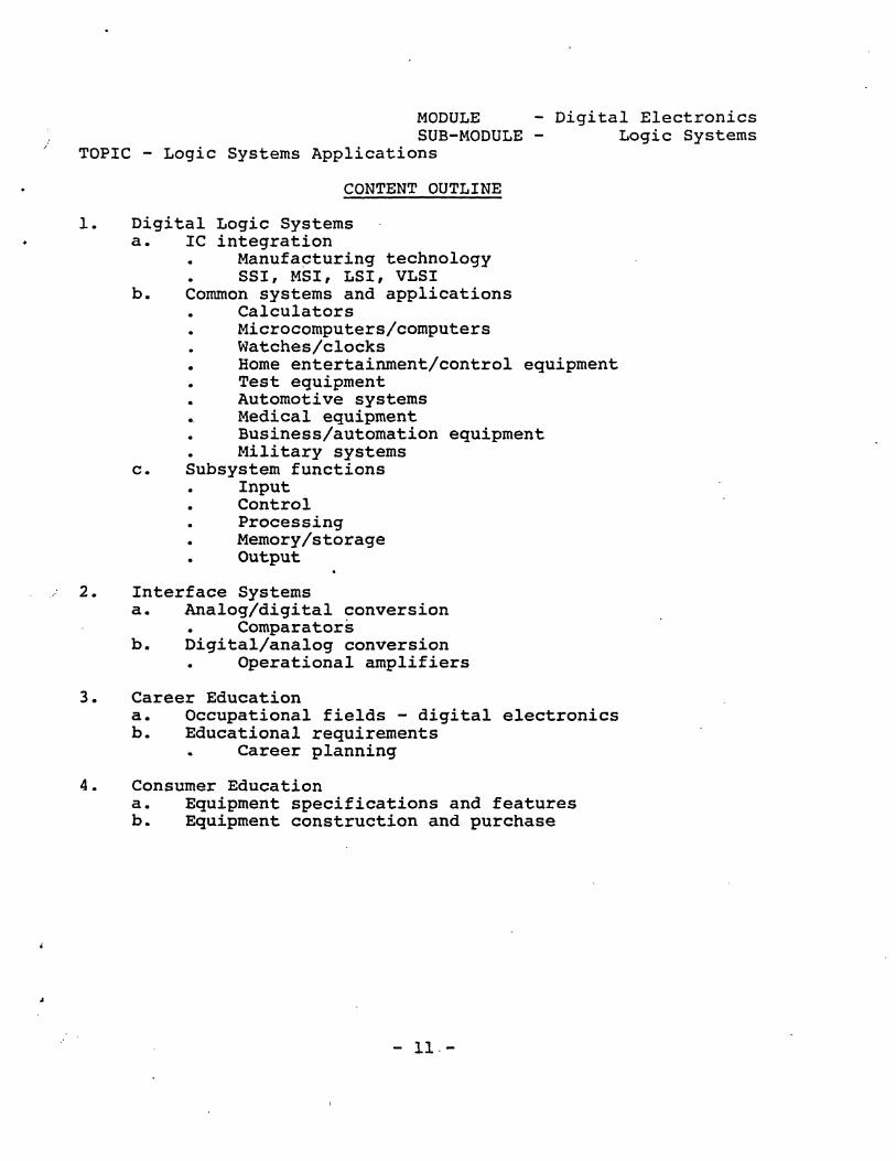
CONTENT OUTLINE
1. Digital Logic Systems a. IC integration
Manufacturing technology SSI, MSI, LSI, VLSI
b. Common systems and applications Calculators Microcomputers/computers Watches/clocks Home entertainment/control equipment Test equipment Automotive systems
.. Medical equipment Business/automation equipment Military systems
c. Subsystem functions Input Control Processing Memory/storage Output
2. Interface Systems a. Analog/digital conversion
Comparators b. Digital/analog conversion
Operational amplifiers
3. Career Education a. Occupational fields - digital electronics b. Educational requirements
Career planning
4. Consumer Education a. Equipment specifications and features b. Equipment construction and purchase
..
- 11-

MODULE - Digital Electronics SUB-MODULE - Logic Systems
TOPIC - Logic Systems Applications
PERFORMANCE OBJECTIVE No. 1:
Given the necessary instruction, the student will list the operations required for integrated circuit manufacturing and differentiate among SSI, MSI, LSI and VLSI methods of integration to a degree of accuracy and completeness considered acceptable to the instructor.
SUPPORTING COMPETENCIES: In order to do this, the student must be able to:
a. Differentiate between monolithic and hybrid methods of IC manufacture.
b. List and identify eight sequential steps required to manufacture a monolithic integrated circuit.
c. Differentiate among the four methods of integration in terms of function and logic system design.
d. Recognize the common advantages and disadvantages of IC circuit technology as compared to discrete components.
INSTRUCTIONAL STRATEGIES:
1. Lecture/discussions - show students examples of monolithic and hybrid methods of manufacture. List and discuss the eight steps in IC manufacturing: circuit design, layout design, photolithographic masks, photoetching/diffusion, probe testing, scribing and breaking, packaging, testing. Use charts, photographs, etc. to illustrate steps. Explain differences in IC integration methods, show examples. and discuss applications.
2. Audio/visual materials - reject boards from computer; samples or models of IC integration; films, filmstrips, video tapes illustrating IC manufacture; instruction sheets for terminology, definitions, specifications, etc.
3. Field visitation - for students to witness IC manufacture or assembly of digital systems with IC's.
4. Home study - have students complete matching or fill-in questions about terminology, manufacturing steps, advantages/disadvantages.
~ 12

MODULE - Digital Electronics SUB-MODULE - Logic Systems
TOPIC - Logic Systems Applications
PERFORMANCE OBJECTIVE No. 2:
Given a functional block diagram for a common digital logic system, the student will analyze and interpret the decision
·making and memory circuit processes performed to a degree of accuracy and completeness considered acceptable to the instructor.
SUPPORTING COMPETENCIES: In order to do this, the student must be able to:
a. Read and interpret basic logic symbols and a schematic for a digital logic system.
b.- Apply digital circuit terminology to input, control, processing, memory and output functions.
c. Identify A/D and D/A interface circuits in digital input/output systems.
d. Trace data handling functions through block and/or schematic diagrams for basic digital systems.
e. Recognize digital and analog waveforms of data.
INSTRUCTIONAL STRATEGIES:
1. Lecture/discussion - explain subsystem functions in digital equipment and appliances. Using illustrative schematics and diagrams, have students match functions to circuits employed. Discuss and list common applications of digital technology as contained in Content Outline.
2 •. Audio/visual materials - use transparencies, charts, slides to illustrate block and schematic diagrams. Trace digital and analog waveforms.
3. Demonstration/discussion - use an actual calculator, clock or test instrument to illustrate data handling functions and signal tracing with various IC integration methods.
4. Laboratory experiment(s) - have students assemble and document operation of A/D and/9r D/A converter circuits.
5. Home study - have students identify logic functions and circuit terminology on sample schematic(s) for simple digital systems.
- 13

MODULE - Digital Electronics SUB-MODULE - Logic Systems
TOPIC - Logic Systems Applications
PERFORMANCE OBJECTIVE No. 3
Given the necessary instruction and information concerning career opportunities in digital electronics technologies, the student will demonstrate an awareness of employment alternatives and personal development to a degree of completeness considered acceptable to the instructor.
SUPPORTING COMPETENCIES: In order to do this, the student must be able to:
a. Identify various career clusters and job opportunities in the field of digital electronics.
b. Recognize personal strengths and weaknesses as they apply to his/her aptitudes and abilities.
c. Locate and interpret career information about a · particular occupation in digital technology.
d. List educational strategies which will increase his/ her employment potential in a digital electronics career.
INSTRUCTIONAL STRATEGIES:
1. Lecture/discussion - identify career clusters related to digital electronic technology. Discuss job descriptions, opportunities, requirements and sources of information.
2. Audio/visual materials - commercial career films, filmstrips or video tapes. Slides illustrating career opportunities in the local area.
3. Resource personnel - local industry personnel, military recruiting agent, college admission personnel, local guidance counselor.
4. Career guidance centers - post secondary educational information, bulletins, catalogs, interest inventories, aptitude tests and other career information.
5. Field trip - to identify career o~portunities in a digital technology.
6. Bulletin board - display of occupational titles, want ads, or posters to illustrate potential employment opportunities.
- 14
MODULE - Digital Electronics SUB-MODULE - Logic Systems
TOPIC - Logic Systems Applications
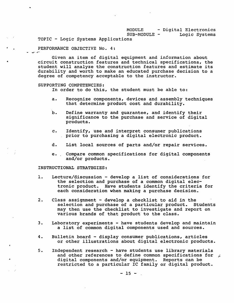
PERFORMANCE OBJECTIVE No. 4:
Given an item of digital equipment and information about .. circuit construction features and technical specifications, the student will analyze the constrtiction features and estimate its durability and worth to make an educated purchase decision to a degree of competency acceptable to the instructor.
SUPPORTING COMPETENCIES: In order to do this, the student must be able to:
a. Recognize components, devices and assembly techniques that determine product cost and durability.
b. Define warranty and guarantee, and identify their significance to the purchase and service of digital products.
c. Identify, use and interpret consumer publications prior to purchasing a digital electronic product.
d. List local sources of parts and/or repair services.
e. Compare common specifications for digital components and/or products.
INSTRUCTIONAL STRATEGIES:
1. Lecture/discussion - develop a list of considerations for the selection and purchase of a common digital electronic product. Have students identify the criteria for each consideration when making a purchase decision.
2. Class assignment - develop a checklist to aid in the selection and purchase of a particular product. Students may then use the checklist to investigate and report on various brands of that product to the class.
3. Laboratory experiments - have students develop and maintain a list of common digital components used and sources.
4. Bulletin board - display consumer publications, articles or other illustrations abou~ digital electronic products.
s. Independent research - have students use library materials and other references to define common specifications for ~ .. digital components and/or equipment. Reports can be restricted to a particular IC family or digital product.
- 15